EP3382897A1 - Control device, in particular for a domestic appliance - Google Patents
Control device, in particular for a domestic appliance Download PDFInfo
- Publication number
- EP3382897A1 EP3382897A1 EP17163227.6A EP17163227A EP3382897A1 EP 3382897 A1 EP3382897 A1 EP 3382897A1 EP 17163227 A EP17163227 A EP 17163227A EP 3382897 A1 EP3382897 A1 EP 3382897A1
- Authority
- EP
- European Patent Office
- Prior art keywords
- control device
- sheet
- conductive layer
- circuit board
- printed circuit
- Prior art date
- Legal status (The legal status is an assumption and is not a legal conclusion. Google has not performed a legal analysis and makes no representation as to the accuracy of the status listed.)
- Granted
Links
Images


Classifications
-
- H—ELECTRICITY
- H03—ELECTRONIC CIRCUITRY
- H03K—PULSE TECHNIQUE
- H03K17/00—Electronic switching or gating, i.e. not by contact-making and –breaking
- H03K17/94—Electronic switching or gating, i.e. not by contact-making and –breaking characterised by the way in which the control signals are generated
- H03K17/96—Touch switches
- H03K17/962—Capacitive touch switches
-
- H—ELECTRICITY
- H03—ELECTRONIC CIRCUITRY
- H03K—PULSE TECHNIQUE
- H03K17/00—Electronic switching or gating, i.e. not by contact-making and –breaking
- H03K17/94—Electronic switching or gating, i.e. not by contact-making and –breaking characterised by the way in which the control signals are generated
- H03K17/96—Touch switches
- H03K2017/9602—Touch switches characterised by the type or shape of the sensing electrodes
-
- H—ELECTRICITY
- H03—ELECTRONIC CIRCUITRY
- H03K—PULSE TECHNIQUE
- H03K2217/00—Indexing scheme related to electronic switching or gating, i.e. not by contact-making or -breaking covered by H03K17/00
- H03K2217/94—Indexing scheme related to electronic switching or gating, i.e. not by contact-making or -breaking covered by H03K17/00 characterised by the way in which the control signal is generated
- H03K2217/96—Touch switches
- H03K2217/9607—Capacitive touch switches
- H03K2217/960755—Constructional details of capacitive touch and proximity switches
Definitions
- the present invention relates to a control device according to the preamble of claim 1.
- the present invention relates to a control device for a domestic appliance according to the preamble of claim 1.
- a control device in particular for a domestic appliance, includes often touch switches.
- said touch switches may be of a capacitive type, an inductive type, an optical type or an infrared type.
- the touch switches do not require any mechanical elements.
- US 2009/0090605 A1 discloses a control device for an electrical appliance.
- the control device includes a front panel and a printed circuit board arranged behind and parallel to said front panel.
- the printed circuit board includes a cut-out. Said cut-out is covered by a polymeric film acting as light filter.
- An annular track is attached at the rear side of the printed circuit board and acts as a touch electrode for a touch switch.
- said touch switch is relative complex.
- control device The object of the present invention is achieved by the control device according to claim 1.
- a conductive layer is applied at the rear side or at the front side of the sheet and arranged in front of the cut-out of the printed circuit board, wherein said conductive layer forms an electrode for a touch sensitive switch.
- the conductive layer applied at the sheet provides the electrode for the touch sensitive switch by low complexity.
- the electrode is arranged in a central position of the touch sensitive switch.
- the sheet is a transparent or opal foil.
- a further conductive layer is applied at the front side or at the rear side, respectively, of the transparent or opal sheet and arranged in front of the cut-out, wherein said further conductive layer forms a further electrode of the touch sensitive switch.
- the conductive layer may be applied at the sheet according to a predefined pattern, wherein preferably the conductive layers at the rear side and front side of the sheet have different patterns.
- At least one electronic and/or electric circuit may be arranged at the rear side of the printed circuit board.
- the conductive layer is or the conductive layers are, respectively, electrically connected to the electronic and/or electric circuit at the printed circuit board.
- the sheet is aligned at the front side of the printed circuit board.
- the rear side of the sheet may be connected to the front side of the printed circuit board by at least one adhesive tape.
- the printed circuit board with the sheet is pressed at the rear side of the front panel by mechanical fastening elements.
- the front side of the sheet may be connected to the rear side of the front panel by at least one further adhesive tape.
- At least one light source element is arranged at the rear side of the printed circuit board, wherein at least one reflector element is arranged behind the cut-out and said light source element.
- the sheet may be made of a dielectric material, wherein preferably the sheet is made of polyethylene terephthalate (PET), polycarbonate (PC) or polyvinyl chloride (PVC).
- PET polyethylene terephthalate
- PC polycarbonate
- PVC polyvinyl chloride
- the sheet may have a thickness between 0.1 mm and 2 mm, preferably between 0.1 mm and 1 mm, in particular between 0.1 mm and 0.5 mm.
- the conductive layer forms an outer electrode, while the further conductive layer forms an inner electrode.
- the conductive layer may enclose a non-conductive area having a predetermined shape, wherein the shape of the further conductive layer is congruent with said predetermine shape.
- FIG 1 illustrates a schematic sectional side view of a control device for an appliance according to a preferred embodiment of the present invention.
- the control device is provided for a domestic appliance.
- the control device comprises a front panel 10, a printed circuit board 22 and a transparent or opal sheet 34.
- the front panel 10, the printed circuit board 22 and the sheet 34 are arranged vertically.
- a front side of the control device is represented on the right hand side of FIG 1
- a rear side of said control device is represented on the left hand side of FIG 1 .
- the printed circuit board 22 is arranged behind the front panel 10.
- the printed circuit board extends parallel to the front panel 10.
- the sheet 34 is arranged in front of the printed circuit board 22.
- the printed circuit board 22 includes a cut-out 12.
- a printed icon 39 and a printed non-switchable area 40 are applied at a rear side of the front panel 10.
- the printed icon 39 is arranged in front of the cut-out 12 formed in the printed circuit board 22, while the printed non-switchable area 40 encloses said printed icon 39.
- the printed icon 39 and the printed non-switchable area 40 are arranged within one plane.
- the control device may comprise one or more printed icons 39 at the rear side of the front panel 10 and one or more cut-outs 12 formed in the printed circuit board 22, wherein the printed icons 39 are arranged in front of corresponding cut-outs 22.
- a conductive layer 50 is applied at the rear side and at the front side of the sheet 34 in each case.
- Said conductive layers are 50 is arranged in front of the cut-out 12 of the printed circuit board 22.
- Said conductive layers 50 form two electrodes for a touch sensitive switch.
- one or more conductive layers 50 are applied at the rear side and/or at the front side of the sheet 34.
- the conductive layers 50 are electrically connected to the rear side of the printed circuit board 22 via two lines 60.
- the sheet 34 with the conductive layers 50 is aligned at the front side of the printed circuit board 22.
- the rear side of the sheet 34 is connected to the front side of the printed circuit board 22 by an adhesive tape 36.
- the sheet 34 is made of a dielectric material.
- the sheet 34 is made of polyethylene terephthalate (PET), polycarbonate (PC), polyvinyl chloride (PVC) or the like.
- the sheet 34 has a thickness between 0.1 mm and 1 mm.
- the printed circuit board 22 with the sheet 34 is pressed at the rear side of the front panel 10 by mechanical fastening elements.
- the front side of the sheet 34 is connected to the rear side of the front panel 10 by at least one further adhesive tape 38.
- control element comprises a number of light source elements 24 and a reflector element 26.
- the light source elements 24 are light emitting diodes (LED).
- the light source elements 24 are arranged at the rear side of the printed circuit board 22.
- the light source elements 24 are arranged beside the cut-out 12 of the printed circuit board 22.
- the reflector element 26 is arranged at the rear side of the printed circuit board 22 and covers the light source elements 24 and the cut-out 12 of the printed circuit board 22. Light generated by the light source elements 24 is reflected by the reflector element 26 and passes the cut-out 12, the adhesive tape 36, the sheet 34, the further adhesive tape 38, the printed icon 39 and the front panel 10.
- FIG 2 illustrates a schematic front view of the sheet 34 with conductive layers 52 and 54 for the control device according to a first embodiment of the present invention.
- a first conductive layer 52 forms an outer electrode, while a second conductive layer 54 forms an inner electrode.
- the first conductive layer 52 and the second conductive layer 54 may be arranged at opposite sides of the sheet 34. Alternatively, the first conductive layer 52 and the second conductive layer 54 may be arranged at the same side of the sheet 34.
- the first conductive layer 52 includes a rectangular path and two tongues. Said tongues extend into the inner area enclosed by said rectangular path. An E-shaped non-conductive area remains inside the first conductive layer 52.
- the second conductive layer 52 is arranged within said E-shaped non-conductive area. The second conductive layer 52 is congruent with the E-shaped non-conductive area. The distance between the first conductive layer 52 and the second conductive layer 54 is minimised.
- FIG 3 illustrates a schematic front view of the sheet 34 with the conductive layers 52 and 54 for the control device according to a second embodiment of the present invention.
- the first conductive layer 52 and the second conductive layer 54 may be arranged either at opposite sides of the sheet 34 or at the same side of the sheet 34.
- the first conductive layer 52 includes a rectangular path and two tongues. Said tongues extend into the inner area enclosed by said rectangular path, wherein an H-shaped non-conductive area remains inside the first conductive layer 52.
- the second conductive layer 52 is arranged within the H-shaped non-conductive area and is congruent with said H-shaped non-conductive area. The distance between the first conductive layer 52 and the second conductive layer 54 is minimised.
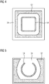
- FIG 4 illustrates a schematic front view of the sheet 34 with the conductive layers 52 and 54 for the control device according to a third embodiment of the present invention.
- the first conductive layer 52 and the second conductive layer 54 may be arranged either at opposite sides of the sheet 34 or at the same side of the sheet 34.
- the first conductive layer 52 is formed as a rectangular path.
- the second conductive layer 52 is also formed as a rectangular path and enclosed by the first conductive layer 52.
- FIG 5 illustrates a schematic front view of the sheet 34 with the conductive layers 52 and 54 for the control device according to a fourth embodiment of the present invention.
- the first conductive layer 52 and the second conductive layer 54 may be arranged either at opposite sides of the sheet 34 or at the same side of the sheet 34.
- the first conductive layer 52 is formed as a U-shaped or horseshoe-shaped path.
- the second conductive layer 52 is also formed as a horseshoe-shaped path and enclosed by the first conductive layer 52.
Landscapes
- Push-Button Switches (AREA)
- Switches That Are Operated By Magnetic Or Electric Fields (AREA)
- Electroluminescent Light Sources (AREA)
Abstract
Description
- The present invention relates to a control device according to the preamble of claim 1. In particular, the present invention relates to a control device for a domestic appliance according to the preamble of claim 1.
- A control device, in particular for a domestic appliance, includes often touch switches. For example, said touch switches may be of a capacitive type, an inductive type, an optical type or an infrared type. The touch switches do not require any mechanical elements.
-
US 2009/0090605 A1 discloses a control device for an electrical appliance. The control device includes a front panel and a printed circuit board arranged behind and parallel to said front panel. The printed circuit board includes a cut-out. Said cut-out is covered by a polymeric film acting as light filter. An annular track is attached at the rear side of the printed circuit board and acts as a touch electrode for a touch switch. However, said touch switch is relative complex. - It is an object of the present invention to provide a control device, which provides a touch switch by low complexity.
- The object of the present invention is achieved by the control device according to claim 1.
- According to the present invention a conductive layer is applied at the rear side or at the front side of the sheet and arranged in front of the cut-out of the printed circuit board, wherein said conductive layer forms an electrode for a touch sensitive switch.
- The conductive layer applied at the sheet provides the electrode for the touch sensitive switch by low complexity. The electrode is arranged in a central position of the touch sensitive switch.
- Preferably, the sheet is a transparent or opal foil.
- In particular, a further conductive layer is applied at the front side or at the rear side, respectively, of the transparent or opal sheet and arranged in front of the cut-out, wherein said further conductive layer forms a further electrode of the touch sensitive switch.
- Further, the conductive layer may be applied at the sheet according to a predefined pattern, wherein preferably the conductive layers at the rear side and front side of the sheet have different patterns.
- Moreover, at least one electronic and/or electric circuit may be arranged at the rear side of the printed circuit board.
- Preferably, the conductive layer is or the conductive layers are, respectively, electrically connected to the electronic and/or electric circuit at the printed circuit board.
- In particular, the sheet is aligned at the front side of the printed circuit board.
- Further, the rear side of the sheet may be connected to the front side of the printed circuit board by at least one adhesive tape.
- For example, the printed circuit board with the sheet is pressed at the rear side of the front panel by mechanical fastening elements.
- Alternatively or additionally, the front side of the sheet may be connected to the rear side of the front panel by at least one further adhesive tape.
- In particular, at least one light source element is arranged at the rear side of the printed circuit board, wherein at least one reflector element is arranged behind the cut-out and said light source element.
- The sheet may be made of a dielectric material, wherein preferably the sheet is made of polyethylene terephthalate (PET), polycarbonate (PC) or polyvinyl chloride (PVC).
- Further, the sheet may have a thickness between 0.1 mm and 2 mm, preferably between 0.1 mm and 1 mm, in particular between 0.1 mm and 0.5 mm.
- For example, the conductive layer forms an outer electrode, while the further conductive layer forms an inner electrode.
- At last, the conductive layer may enclose a non-conductive area having a predetermined shape, wherein the shape of the further conductive layer is congruent with said predetermine shape.
- Novel and inventive features of the present invention are set forth in the appended claims.
- The present invention will be described in further detail with reference to the drawing, in which
- FIG 1
- illustrates a schematic sectional side view of a control device according to a preferred embodiment of the present invention,
- FIG 2
- illustrates a schematic front view of a sheet with conductive layers for the control device according to a first embodiment of the present invention,
- FIG 3
- illustrates a schematic front view of the sheet with the conductive layers for the control device according to a second embodiment of the present invention,
- FIG 4
- illustrates a schematic front view of the sheet with the conductive layers for the control device according to a third embodiment of the present invention, and
- FIG 5
- illustrates a schematic front view of the sheet with the conductive layers for the control device according to a fourth embodiment of the present invention.
-
FIG 1 illustrates a schematic sectional side view of a control device for an appliance according to a preferred embodiment of the present invention. In this example, the control device is provided for a domestic appliance. - The control device comprises a
front panel 10, aprinted circuit board 22 and a transparent oropal sheet 34. In this example, thefront panel 10, the printedcircuit board 22 and thesheet 34 are arranged vertically. A front side of the control device is represented on the right hand side ofFIG 1 , while a rear side of said control device is represented on the left hand side ofFIG 1 . The printedcircuit board 22 is arranged behind thefront panel 10. The printed circuit board extends parallel to thefront panel 10. Thesheet 34 is arranged in front of the printedcircuit board 22. - The printed
circuit board 22 includes a cut-out 12. A printedicon 39 and a printednon-switchable area 40 are applied at a rear side of thefront panel 10. The printedicon 39 is arranged in front of the cut-out 12 formed in the printedcircuit board 22, while the printednon-switchable area 40 encloses said printedicon 39. The printedicon 39 and the printednon-switchable area 40 are arranged within one plane. In general, the control device may comprise one or more printedicons 39 at the rear side of thefront panel 10 and one or more cut-outs 12 formed in the printedcircuit board 22, wherein the printedicons 39 are arranged in front of corresponding cut-outs 22. - A
conductive layer 50 is applied at the rear side and at the front side of thesheet 34 in each case. Said conductive layers are 50 is arranged in front of the cut-out 12 of the printedcircuit board 22. Saidconductive layers 50 form two electrodes for a touch sensitive switch. In general, one or moreconductive layers 50 are applied at the rear side and/or at the front side of thesheet 34. Theconductive layers 50 are electrically connected to the rear side of the printedcircuit board 22 via twolines 60. Preferably, thesheet 34 with theconductive layers 50 is aligned at the front side of the printedcircuit board 22. In this example, the rear side of thesheet 34 is connected to the front side of the printedcircuit board 22 by anadhesive tape 36. Thesheet 34 is made of a dielectric material. For example, thesheet 34 is made of polyethylene terephthalate (PET), polycarbonate (PC), polyvinyl chloride (PVC) or the like. Preferably, thesheet 34 has a thickness between 0.1 mm and 1 mm. - Optionally, the printed
circuit board 22 with thesheet 34 is pressed at the rear side of thefront panel 10 by mechanical fastening elements. Alternatively or additionally, the front side of thesheet 34 is connected to the rear side of thefront panel 10 by at least one furtheradhesive tape 38. - Further, the control element comprises a number of
light source elements 24 and areflector element 26. Preferably, thelight source elements 24 are light emitting diodes (LED). Thelight source elements 24 are arranged at the rear side of the printedcircuit board 22. Preferably, thelight source elements 24 are arranged beside the cut-out 12 of the printedcircuit board 22. Thereflector element 26 is arranged at the rear side of the printedcircuit board 22 and covers thelight source elements 24 and the cut-out 12 of the printedcircuit board 22. Light generated by thelight source elements 24 is reflected by thereflector element 26 and passes the cut-out 12, theadhesive tape 36, thesheet 34, the furtheradhesive tape 38, the printedicon 39 and thefront panel 10. -
FIG 2 illustrates a schematic front view of thesheet 34 withconductive layers - A first
conductive layer 52 forms an outer electrode, while a secondconductive layer 54 forms an inner electrode. The firstconductive layer 52 and the secondconductive layer 54 may be arranged at opposite sides of thesheet 34. Alternatively, the firstconductive layer 52 and the secondconductive layer 54 may be arranged at the same side of thesheet 34. - The first
conductive layer 52 includes a rectangular path and two tongues. Said tongues extend into the inner area enclosed by said rectangular path. An E-shaped non-conductive area remains inside the firstconductive layer 52. The secondconductive layer 52 is arranged within said E-shaped non-conductive area. The secondconductive layer 52 is congruent with the E-shaped non-conductive area. The distance between the firstconductive layer 52 and the secondconductive layer 54 is minimised. -
FIG 3 illustrates a schematic front view of thesheet 34 with theconductive layers conductive layer 52 and the secondconductive layer 54 may be arranged either at opposite sides of thesheet 34 or at the same side of thesheet 34. - The first
conductive layer 52 includes a rectangular path and two tongues. Said tongues extend into the inner area enclosed by said rectangular path, wherein an H-shaped non-conductive area remains inside the firstconductive layer 52. The secondconductive layer 52 is arranged within the H-shaped non-conductive area and is congruent with said H-shaped non-conductive area. The distance between the firstconductive layer 52 and the secondconductive layer 54 is minimised. -
FIG 4 illustrates a schematic front view of thesheet 34 with theconductive layers conductive layer 52 and the secondconductive layer 54 may be arranged either at opposite sides of thesheet 34 or at the same side of thesheet 34. - The first
conductive layer 52 is formed as a rectangular path. The secondconductive layer 52 is also formed as a rectangular path and enclosed by the firstconductive layer 52. -
FIG 5 illustrates a schematic front view of thesheet 34 with theconductive layers conductive layer 52 and the secondconductive layer 54 may be arranged either at opposite sides of thesheet 34 or at the same side of thesheet 34. - The first
conductive layer 52 is formed as a U-shaped or horseshoe-shaped path. The secondconductive layer 52 is also formed as a horseshoe-shaped path and enclosed by the firstconductive layer 52. - Although an illustrative embodiment of the present invention has been described herein with reference to the accompanying drawings, it is to be understood that the present invention is not limited to that precise embodiment, and that various other changes and modifications may be affected therein by one skilled in the art without departing from the scope or spirit of the invention. All such changes and modifications are intended to be included within the scope of the invention as defined by the appended claims.
-
- 10
- front panel
- 12
- cut-out
- 22
- printed circuit board
- 24
- light source element
- 26
- reflector element
- 34
- transparent or opal sheet
- 36
- adhesive layer
- 38
- further adhesive layer
- 39
- printed icon
- 40
- printed non-switchable area
- 50
- conductive layer
- 52
- first conductive layer
- 54
- second conductive layer
- 60
- line
Claims (15)
- A control device, in particular for a domestic appliance, wherein:- the control device comprises at least one front panel (10),- the control device comprises at least one printed circuit board (22) arranged behind and parallel to the front panel (10),- the printed circuit board (22) includes at least one cut-out (12), and- the control device comprises at least one transparent or opal sheet (34) arranged in front of the printed circuit board (22),characterised in that
a conductive layer (50; 52, 54) is applied at the rear side or at the front side of the sheet (34) and arranged in front of the cut-out (12) of the printed circuit board (22), wherein said conductive layer (50; 52, 54) forms an electrode for a touch sensitive switch. - The control device according to claim 1,
characterised in that
the sheet (34) is a transparent or opal foil (34). - The control device according to claim 1 or 2, characterised in that
a further conductive layer (50; 52, 54) is applied at the front side or at the rear side, respectively, of the transparent or opal sheet (34) and arranged in front of the cut-out (12), wherein said further conductive layer (50; 52, 54) forms a further electrode of the touch sensitive switch. - The control device according to any one of the preceding claims,
characterised in that
the conductive layer (50; 52, 54) is applied at the sheet (34) according to a predefined pattern, wherein preferably the conductive layers (50; 52, 54) at the rear side and front side of the sheet (34) have different patterns. - The control device according to any one of the preceding claims,
characterised in that
at least one electronic and/or electric circuit is arranged at the rear side of the printed circuit board (22). - The control device according to any one of the preceding claims,
characterised in that
the conductive layer (50; 52, 54) is or the conductive layers (50; 52, 54) are, respectively, electrically connected to the electronic and/or electric circuit at the printed circuit board (22). - The control device according to any one of the preceding claims,
characterised in that
the sheet (34) is aligned at the front side of the printed circuit board (22). - The control device according to any one of the preceding claims,
characterised in that
the rear side of the sheet (34) is connected to the front side of the printed circuit board (22) by at least one adhesive tape (36). - The control device according to any one of the preceding claims,
characterised in that
the printed circuit board (22) with the sheet (34) is pressed at the rear side of the front panel (10) by mechanical fastening elements. - The control device according to any one of the claims 1 to 8,
characterised in that
the front side of the sheet (34) is connected to the rear side of the front panel (10) by at least one further adhesive tape (38). - The control device according to any one of the preceding claims,
characterised in that
at least one light source element (24) is arranged at the rear side of the printed circuit board (22), wherein at least one reflector element (26) is arranged behind the cut-out (12) and said light source element (24). - The control device according to any one of the preceding claims,
characterised in that
the sheet (34) is made of a dielectric material, wherein preferably the sheet (34) is made of polyethylene terephthalate (PET), polycarbonate (PC) or polyvinyl chloride (PVC). - The control device according to any one of the preceding claims,
characterised in that
the sheet (34) has a thickness between 0.1 mm and 2 mm, preferably between 0.1 mm and 1 mm, in particular between 0.1 mm and 0.5 mm. - The control device according to any one of the preceding claims,
characterised in that
the conductive layer (52) forms an outer electrode, while the further conductive layer (54) forms an inner electrode. - The control device according to claim 14,
characterised in that
the conductive layer (52) encloses a non-conductive area having a predetermined shape, wherein the shape of the further conductive layer (54) is congruent with said predetermine shape.
Priority Applications (4)
| Application Number | Priority Date | Filing Date | Title |
|---|---|---|---|
| EP17163227.6A EP3382897B1 (en) | 2017-03-28 | 2017-03-28 | Control device, in particular for a domestic appliance |
| AU2018242130A AU2018242130A1 (en) | 2017-03-28 | 2018-03-12 | Control device, in particular for a domestic appliance |
| PCT/EP2018/056016 WO2018177726A1 (en) | 2017-03-28 | 2018-03-12 | Control device, in particular for a domestic appliance |
| BR112019019229-8A BR112019019229B1 (en) | 2017-03-28 | 2018-03-12 | CONTROL DEVICE |
Applications Claiming Priority (1)
| Application Number | Priority Date | Filing Date | Title |
|---|---|---|---|
| EP17163227.6A EP3382897B1 (en) | 2017-03-28 | 2017-03-28 | Control device, in particular for a domestic appliance |
Publications (2)
| Publication Number | Publication Date |
|---|---|
| EP3382897A1 true EP3382897A1 (en) | 2018-10-03 |
| EP3382897B1 EP3382897B1 (en) | 2022-06-01 |
Family
ID=58461074
Family Applications (1)
| Application Number | Title | Priority Date | Filing Date |
|---|---|---|---|
| EP17163227.6A Active EP3382897B1 (en) | 2017-03-28 | 2017-03-28 | Control device, in particular for a domestic appliance |
Country Status (3)
| Country | Link |
|---|---|
| EP (1) | EP3382897B1 (en) |
| AU (1) | AU2018242130A1 (en) |
| WO (1) | WO2018177726A1 (en) |
Citations (4)
| Publication number | Priority date | Publication date | Assignee | Title |
|---|---|---|---|---|
| EP1542363A1 (en) * | 2002-09-10 | 2005-06-15 | Azkoyen Industrial, S.A. | Keypad for vending machines |
| EP1816747A2 (en) * | 2006-02-06 | 2007-08-08 | Diehl AKO Stiftung & Co. KG | Capacitive touch switch |
| US20090090605A1 (en) | 2007-10-08 | 2009-04-09 | Whirlpool Corporation | Touch switch for electrical appliances and electrical appliance provided with such switch |
| EP2690786A1 (en) * | 2012-07-25 | 2014-01-29 | Electrolux Home Products Corporation N.V. | A control device, in particular for a domestic appliance |
Family Cites Families (3)
| Publication number | Priority date | Publication date | Assignee | Title |
|---|---|---|---|---|
| US8638314B2 (en) * | 2008-10-17 | 2014-01-28 | Atmel Corporation | Capacitive touch buttons combined with electroluminescent lighting |
| TW201443723A (en) * | 2013-05-10 | 2014-11-16 | Wintek Corp | Touch sensing unit and touch panel |
| DE102013112651A1 (en) * | 2013-11-15 | 2015-05-21 | Polyic Gmbh & Co. Kg | Multi-layer body to provide a transparent keyboard functionality |
-
2017
- 2017-03-28 EP EP17163227.6A patent/EP3382897B1/en active Active
-
2018
- 2018-03-12 AU AU2018242130A patent/AU2018242130A1/en not_active Abandoned
- 2018-03-12 WO PCT/EP2018/056016 patent/WO2018177726A1/en not_active Ceased
Patent Citations (4)
| Publication number | Priority date | Publication date | Assignee | Title |
|---|---|---|---|---|
| EP1542363A1 (en) * | 2002-09-10 | 2005-06-15 | Azkoyen Industrial, S.A. | Keypad for vending machines |
| EP1816747A2 (en) * | 2006-02-06 | 2007-08-08 | Diehl AKO Stiftung & Co. KG | Capacitive touch switch |
| US20090090605A1 (en) | 2007-10-08 | 2009-04-09 | Whirlpool Corporation | Touch switch for electrical appliances and electrical appliance provided with such switch |
| EP2690786A1 (en) * | 2012-07-25 | 2014-01-29 | Electrolux Home Products Corporation N.V. | A control device, in particular for a domestic appliance |
Also Published As
| Publication number | Publication date |
|---|---|
| AU2018242130A1 (en) | 2019-08-22 |
| BR112019019229A2 (en) | 2020-04-14 |
| WO2018177726A1 (en) | 2018-10-04 |
| EP3382897B1 (en) | 2022-06-01 |
Similar Documents
| Publication | Publication Date | Title |
|---|---|---|
| EP1039493B1 (en) | El-combined sheet switch | |
| EP2690786A1 (en) | A control device, in particular for a domestic appliance | |
| EP2662981A1 (en) | Capacitive proximity and/or contact switch avec floating electrode | |
| JP2008181709A (en) | Sheet member for operating switch and operating switch | |
| JP4494164B2 (en) | Capacitance type switch device | |
| EP3142468B1 (en) | Flexible printed circuit board and method of folding a flexible printed circuit board | |
| CN111124167A (en) | touch display device | |
| CN105874276A (en) | Operating device for domestic appliance | |
| JPWO2017183315A1 (en) | Capacitive sensor | |
| US20180248547A1 (en) | Capacitive touch switch, configuration of capacitive touch switches and operating device | |
| EP3382897B1 (en) | Control device, in particular for a domestic appliance | |
| JP6300025B2 (en) | Film fixing structure and film fixing method | |
| CN118519545A (en) | Detecting user input in a vehicle with integrated capacitive compensation | |
| US20150116221A1 (en) | Touch mouse and touch control circuit board thereof | |
| JP6098305B2 (en) | Capacitive switch | |
| JP2016148926A (en) | Touch panel sensor, touch panel device, and conductive pattern substrate | |
| CN110771275B (en) | Functional electromagnetic interference shield assembly for plugging a housing opening | |
| KR101964856B1 (en) | Touch pad for icon light point lighting using laser direct structuring technique | |
| JP6040925B2 (en) | Capacitive switch | |
| JP2017139165A (en) | Mirror device | |
| CN113614682A (en) | Touch sensor | |
| CN204066076U (en) | A kind of touch panel display device | |
| US11757447B2 (en) | Sensor element device for an operating device, operating device and electrical appliance having such an operating device | |
| TWI739073B (en) | Electric-heating apparatus and touch device therein | |
| JP6044423B2 (en) | Capacitive switch |
Legal Events
| Date | Code | Title | Description |
|---|---|---|---|
| PUAI | Public reference made under article 153(3) epc to a published international application that has entered the european phase |
Free format text: ORIGINAL CODE: 0009012 |
|
| STAA | Information on the status of an ep patent application or granted ep patent |
Free format text: STATUS: THE APPLICATION HAS BEEN PUBLISHED |
|
| AK | Designated contracting states |
Kind code of ref document: A1 Designated state(s): AL AT BE BG CH CY CZ DE DK EE ES FI FR GB GR HR HU IE IS IT LI LT LU LV MC MK MT NL NO PL PT RO RS SE SI SK SM TR |
|
| AX | Request for extension of the european patent |
Extension state: BA ME |
|
| STAA | Information on the status of an ep patent application or granted ep patent |
Free format text: STATUS: REQUEST FOR EXAMINATION WAS MADE |
|
| 17P | Request for examination filed |
Effective date: 20190403 |
|
| RBV | Designated contracting states (corrected) |
Designated state(s): AL AT BE BG CH CY CZ DE DK EE ES FI FR GB GR HR HU IE IS IT LI LT LU LV MC MK MT NL NO PL PT RO RS SE SI SK SM TR |
|
| STAA | Information on the status of an ep patent application or granted ep patent |
Free format text: STATUS: EXAMINATION IS IN PROGRESS |
|
| 17Q | First examination report despatched |
Effective date: 20200701 |
|
| GRAP | Despatch of communication of intention to grant a patent |
Free format text: ORIGINAL CODE: EPIDOSNIGR1 |
|
| STAA | Information on the status of an ep patent application or granted ep patent |
Free format text: STATUS: GRANT OF PATENT IS INTENDED |
|
| INTG | Intention to grant announced |
Effective date: 20220110 |
|
| GRAS | Grant fee paid |
Free format text: ORIGINAL CODE: EPIDOSNIGR3 |
|
| GRAA | (expected) grant |
Free format text: ORIGINAL CODE: 0009210 |
|
| STAA | Information on the status of an ep patent application or granted ep patent |
Free format text: STATUS: THE PATENT HAS BEEN GRANTED |
|
| AK | Designated contracting states |
Kind code of ref document: B1 Designated state(s): AL AT BE BG CH CY CZ DE DK EE ES FI FR GB GR HR HU IE IS IT LI LT LU LV MC MK MT NL NO PL PT RO RS SE SI SK SM TR |
|
| REG | Reference to a national code |
Ref country code: GB Ref legal event code: FG4D |
|
| REG | Reference to a national code |
Ref country code: AT Ref legal event code: REF Ref document number: 1496101 Country of ref document: AT Kind code of ref document: T Effective date: 20220615 Ref country code: CH Ref legal event code: EP |
|
| REG | Reference to a national code |
Ref country code: IE Ref legal event code: FG4D |
|
| REG | Reference to a national code |
Ref country code: DE Ref legal event code: R096 Ref document number: 602017057931 Country of ref document: DE |
|
| REG | Reference to a national code |
Ref country code: LT Ref legal event code: MG9D |
|
| REG | Reference to a national code |
Ref country code: NL Ref legal event code: MP Effective date: 20220601 |
|
| PG25 | Lapsed in a contracting state [announced via postgrant information from national office to epo] |
Ref country code: SE Free format text: LAPSE BECAUSE OF FAILURE TO SUBMIT A TRANSLATION OF THE DESCRIPTION OR TO PAY THE FEE WITHIN THE PRESCRIBED TIME-LIMIT Effective date: 20220601 Ref country code: NO Free format text: LAPSE BECAUSE OF FAILURE TO SUBMIT A TRANSLATION OF THE DESCRIPTION OR TO PAY THE FEE WITHIN THE PRESCRIBED TIME-LIMIT Effective date: 20220901 Ref country code: LT Free format text: LAPSE BECAUSE OF FAILURE TO SUBMIT A TRANSLATION OF THE DESCRIPTION OR TO PAY THE FEE WITHIN THE PRESCRIBED TIME-LIMIT Effective date: 20220601 Ref country code: HR Free format text: LAPSE BECAUSE OF FAILURE TO SUBMIT A TRANSLATION OF THE DESCRIPTION OR TO PAY THE FEE WITHIN THE PRESCRIBED TIME-LIMIT Effective date: 20220601 Ref country code: GR Free format text: LAPSE BECAUSE OF FAILURE TO SUBMIT A TRANSLATION OF THE DESCRIPTION OR TO PAY THE FEE WITHIN THE PRESCRIBED TIME-LIMIT Effective date: 20220902 Ref country code: FI Free format text: LAPSE BECAUSE OF FAILURE TO SUBMIT A TRANSLATION OF THE DESCRIPTION OR TO PAY THE FEE WITHIN THE PRESCRIBED TIME-LIMIT Effective date: 20220601 Ref country code: ES Free format text: LAPSE BECAUSE OF FAILURE TO SUBMIT A TRANSLATION OF THE DESCRIPTION OR TO PAY THE FEE WITHIN THE PRESCRIBED TIME-LIMIT Effective date: 20220601 Ref country code: BG Free format text: LAPSE BECAUSE OF FAILURE TO SUBMIT A TRANSLATION OF THE DESCRIPTION OR TO PAY THE FEE WITHIN THE PRESCRIBED TIME-LIMIT Effective date: 20220901 |
|
| REG | Reference to a national code |
Ref country code: AT Ref legal event code: MK05 Ref document number: 1496101 Country of ref document: AT Kind code of ref document: T Effective date: 20220601 |
|
| PG25 | Lapsed in a contracting state [announced via postgrant information from national office to epo] |
Ref country code: RS Free format text: LAPSE BECAUSE OF FAILURE TO SUBMIT A TRANSLATION OF THE DESCRIPTION OR TO PAY THE FEE WITHIN THE PRESCRIBED TIME-LIMIT Effective date: 20220601 Ref country code: PL Free format text: LAPSE BECAUSE OF FAILURE TO SUBMIT A TRANSLATION OF THE DESCRIPTION OR TO PAY THE FEE WITHIN THE PRESCRIBED TIME-LIMIT Effective date: 20220601 Ref country code: LV Free format text: LAPSE BECAUSE OF FAILURE TO SUBMIT A TRANSLATION OF THE DESCRIPTION OR TO PAY THE FEE WITHIN THE PRESCRIBED TIME-LIMIT Effective date: 20220601 |
|
| PG25 | Lapsed in a contracting state [announced via postgrant information from national office to epo] |
Ref country code: NL Free format text: LAPSE BECAUSE OF FAILURE TO SUBMIT A TRANSLATION OF THE DESCRIPTION OR TO PAY THE FEE WITHIN THE PRESCRIBED TIME-LIMIT Effective date: 20220601 |
|
| PG25 | Lapsed in a contracting state [announced via postgrant information from national office to epo] |
Ref country code: SM Free format text: LAPSE BECAUSE OF FAILURE TO SUBMIT A TRANSLATION OF THE DESCRIPTION OR TO PAY THE FEE WITHIN THE PRESCRIBED TIME-LIMIT Effective date: 20220601 Ref country code: SK Free format text: LAPSE BECAUSE OF FAILURE TO SUBMIT A TRANSLATION OF THE DESCRIPTION OR TO PAY THE FEE WITHIN THE PRESCRIBED TIME-LIMIT Effective date: 20220601 Ref country code: RO Free format text: LAPSE BECAUSE OF FAILURE TO SUBMIT A TRANSLATION OF THE DESCRIPTION OR TO PAY THE FEE WITHIN THE PRESCRIBED TIME-LIMIT Effective date: 20220601 Ref country code: PT Free format text: LAPSE BECAUSE OF FAILURE TO SUBMIT A TRANSLATION OF THE DESCRIPTION OR TO PAY THE FEE WITHIN THE PRESCRIBED TIME-LIMIT Effective date: 20221003 Ref country code: EE Free format text: LAPSE BECAUSE OF FAILURE TO SUBMIT A TRANSLATION OF THE DESCRIPTION OR TO PAY THE FEE WITHIN THE PRESCRIBED TIME-LIMIT Effective date: 20220601 Ref country code: CZ Free format text: LAPSE BECAUSE OF FAILURE TO SUBMIT A TRANSLATION OF THE DESCRIPTION OR TO PAY THE FEE WITHIN THE PRESCRIBED TIME-LIMIT Effective date: 20220601 Ref country code: AT Free format text: LAPSE BECAUSE OF FAILURE TO SUBMIT A TRANSLATION OF THE DESCRIPTION OR TO PAY THE FEE WITHIN THE PRESCRIBED TIME-LIMIT Effective date: 20220601 |
|
| PG25 | Lapsed in a contracting state [announced via postgrant information from national office to epo] |
Ref country code: IS Free format text: LAPSE BECAUSE OF FAILURE TO SUBMIT A TRANSLATION OF THE DESCRIPTION OR TO PAY THE FEE WITHIN THE PRESCRIBED TIME-LIMIT Effective date: 20221001 |
|
| REG | Reference to a national code |
Ref country code: DE Ref legal event code: R097 Ref document number: 602017057931 Country of ref document: DE |
|
| PG25 | Lapsed in a contracting state [announced via postgrant information from national office to epo] |
Ref country code: AL Free format text: LAPSE BECAUSE OF FAILURE TO SUBMIT A TRANSLATION OF THE DESCRIPTION OR TO PAY THE FEE WITHIN THE PRESCRIBED TIME-LIMIT Effective date: 20220601 |
|
| PLBE | No opposition filed within time limit |
Free format text: ORIGINAL CODE: 0009261 |
|
| STAA | Information on the status of an ep patent application or granted ep patent |
Free format text: STATUS: NO OPPOSITION FILED WITHIN TIME LIMIT |
|
| PG25 | Lapsed in a contracting state [announced via postgrant information from national office to epo] |
Ref country code: DK Free format text: LAPSE BECAUSE OF FAILURE TO SUBMIT A TRANSLATION OF THE DESCRIPTION OR TO PAY THE FEE WITHIN THE PRESCRIBED TIME-LIMIT Effective date: 20220601 |
|
| 26N | No opposition filed |
Effective date: 20230302 |
|
| PG25 | Lapsed in a contracting state [announced via postgrant information from national office to epo] |
Ref country code: SI Free format text: LAPSE BECAUSE OF FAILURE TO SUBMIT A TRANSLATION OF THE DESCRIPTION OR TO PAY THE FEE WITHIN THE PRESCRIBED TIME-LIMIT Effective date: 20220601 |
|
| P01 | Opt-out of the competence of the unified patent court (upc) registered |
Effective date: 20230625 |
|
| PG25 | Lapsed in a contracting state [announced via postgrant information from national office to epo] |
Ref country code: MC Free format text: LAPSE BECAUSE OF FAILURE TO SUBMIT A TRANSLATION OF THE DESCRIPTION OR TO PAY THE FEE WITHIN THE PRESCRIBED TIME-LIMIT Effective date: 20220601 |
|
| REG | Reference to a national code |
Ref country code: CH Ref legal event code: PL |
|
| GBPC | Gb: european patent ceased through non-payment of renewal fee |
Effective date: 20230328 |
|
| REG | Reference to a national code |
Ref country code: BE Ref legal event code: MM Effective date: 20230331 |
|
| PG25 | Lapsed in a contracting state [announced via postgrant information from national office to epo] |
Ref country code: LU Free format text: LAPSE BECAUSE OF NON-PAYMENT OF DUE FEES Effective date: 20230328 |
|
| REG | Reference to a national code |
Ref country code: IE Ref legal event code: MM4A |
|
| PG25 | Lapsed in a contracting state [announced via postgrant information from national office to epo] |
Ref country code: GB Free format text: LAPSE BECAUSE OF NON-PAYMENT OF DUE FEES Effective date: 20230328 |
|
| PG25 | Lapsed in a contracting state [announced via postgrant information from national office to epo] |
Ref country code: LI Free format text: LAPSE BECAUSE OF NON-PAYMENT OF DUE FEES Effective date: 20230331 Ref country code: IE Free format text: LAPSE BECAUSE OF NON-PAYMENT OF DUE FEES Effective date: 20230328 Ref country code: GB Free format text: LAPSE BECAUSE OF NON-PAYMENT OF DUE FEES Effective date: 20230328 Ref country code: CH Free format text: LAPSE BECAUSE OF NON-PAYMENT OF DUE FEES Effective date: 20230331 |
|
| PG25 | Lapsed in a contracting state [announced via postgrant information from national office to epo] |
Ref country code: BE Free format text: LAPSE BECAUSE OF NON-PAYMENT OF DUE FEES Effective date: 20230331 |
|
| PG25 | Lapsed in a contracting state [announced via postgrant information from national office to epo] |
Ref country code: BG Free format text: LAPSE BECAUSE OF FAILURE TO SUBMIT A TRANSLATION OF THE DESCRIPTION OR TO PAY THE FEE WITHIN THE PRESCRIBED TIME-LIMIT Effective date: 20220601 |
|
| PG25 | Lapsed in a contracting state [announced via postgrant information from national office to epo] |
Ref country code: BG Free format text: LAPSE BECAUSE OF FAILURE TO SUBMIT A TRANSLATION OF THE DESCRIPTION OR TO PAY THE FEE WITHIN THE PRESCRIBED TIME-LIMIT Effective date: 20220601 |
|
| PGFP | Annual fee paid to national office [announced via postgrant information from national office to epo] |
Ref country code: FR Payment date: 20250324 Year of fee payment: 9 |
|
| PGFP | Annual fee paid to national office [announced via postgrant information from national office to epo] |
Ref country code: IT Payment date: 20250321 Year of fee payment: 9 |
|
| PG25 | Lapsed in a contracting state [announced via postgrant information from national office to epo] |
Ref country code: CY Free format text: LAPSE BECAUSE OF FAILURE TO SUBMIT A TRANSLATION OF THE DESCRIPTION OR TO PAY THE FEE WITHIN THE PRESCRIBED TIME-LIMIT; INVALID AB INITIO Effective date: 20170328 |
|
| PG25 | Lapsed in a contracting state [announced via postgrant information from national office to epo] |
Ref country code: HU Free format text: LAPSE BECAUSE OF FAILURE TO SUBMIT A TRANSLATION OF THE DESCRIPTION OR TO PAY THE FEE WITHIN THE PRESCRIBED TIME-LIMIT; INVALID AB INITIO Effective date: 20170328 |
|
| PG25 | Lapsed in a contracting state [announced via postgrant information from national office to epo] |
Ref country code: TR Free format text: LAPSE BECAUSE OF FAILURE TO SUBMIT A TRANSLATION OF THE DESCRIPTION OR TO PAY THE FEE WITHIN THE PRESCRIBED TIME-LIMIT Effective date: 20220601 |
|
| PGFP | Annual fee paid to national office [announced via postgrant information from national office to epo] |
Ref country code: DE Payment date: 20260320 Year of fee payment: 10 |