EP3382761A1 - Integration of silicon-germanium semiconductor structures - Google Patents
Integration of silicon-germanium semiconductor structures Download PDFInfo
- Publication number
- EP3382761A1 EP3382761A1 EP17163709.3A EP17163709A EP3382761A1 EP 3382761 A1 EP3382761 A1 EP 3382761A1 EP 17163709 A EP17163709 A EP 17163709A EP 3382761 A1 EP3382761 A1 EP 3382761A1
- Authority
- EP
- European Patent Office
- Prior art keywords
- structures
- subset
- semiconductor device
- nanowires
- source
- Prior art date
- Legal status (The legal status is an assumption and is not a legal conclusion. Google has not performed a legal analysis and makes no representation as to the accuracy of the status listed.)
- Withdrawn
Links
Images

Classifications
-
- H—ELECTRICITY
- H10—SEMICONDUCTOR DEVICES; ELECTRIC SOLID-STATE DEVICES NOT OTHERWISE PROVIDED FOR
- H10D—INORGANIC ELECTRIC SEMICONDUCTOR DEVICES
- H10D84/00—Integrated devices formed in or on semiconductor substrates that comprise only semiconducting layers, e.g. on Si wafers or on GaAs-on-Si wafers
- H10D84/01—Manufacture or treatment
- H10D84/0123—Integrating together multiple components covered by H10D12/00 or H10D30/00, e.g. integrating multiple IGBTs
-
- B—PERFORMING OPERATIONS; TRANSPORTING
- B82—NANOTECHNOLOGY
- B82Y—SPECIFIC USES OR APPLICATIONS OF NANOSTRUCTURES; MEASUREMENT OR ANALYSIS OF NANOSTRUCTURES; MANUFACTURE OR TREATMENT OF NANOSTRUCTURES
- B82Y10/00—Nanotechnology for information processing, storage or transmission, e.g. quantum computing or single electron logic
-
- H—ELECTRICITY
- H10—SEMICONDUCTOR DEVICES; ELECTRIC SOLID-STATE DEVICES NOT OTHERWISE PROVIDED FOR
- H10D—INORGANIC ELECTRIC SEMICONDUCTOR DEVICES
- H10D30/00—Field-effect transistors [FET]
- H10D30/01—Manufacture or treatment
- H10D30/014—Manufacture or treatment of FETs having zero-dimensional [0D] or one-dimensional [1D] channels, e.g. quantum wire FETs, single-electron transistors [SET] or Coulomb blockade transistors
-
- H—ELECTRICITY
- H10—SEMICONDUCTOR DEVICES; ELECTRIC SOLID-STATE DEVICES NOT OTHERWISE PROVIDED FOR
- H10D—INORGANIC ELECTRIC SEMICONDUCTOR DEVICES
- H10D30/00—Field-effect transistors [FET]
- H10D30/01—Manufacture or treatment
- H10D30/021—Manufacture or treatment of FETs having insulated gates [IGFET]
- H10D30/031—Manufacture or treatment of FETs having insulated gates [IGFET] of thin-film transistors [TFT]
-
- H—ELECTRICITY
- H10—SEMICONDUCTOR DEVICES; ELECTRIC SOLID-STATE DEVICES NOT OTHERWISE PROVIDED FOR
- H10D—INORGANIC ELECTRIC SEMICONDUCTOR DEVICES
- H10D30/00—Field-effect transistors [FET]
- H10D30/01—Manufacture or treatment
- H10D30/021—Manufacture or treatment of FETs having insulated gates [IGFET]
- H10D30/031—Manufacture or treatment of FETs having insulated gates [IGFET] of thin-film transistors [TFT]
- H10D30/0321—Manufacture or treatment of FETs having insulated gates [IGFET] of thin-film transistors [TFT] comprising silicon, e.g. amorphous silicon or polysilicon
- H10D30/0323—Manufacture or treatment of FETs having insulated gates [IGFET] of thin-film transistors [TFT] comprising silicon, e.g. amorphous silicon or polysilicon comprising monocrystalline silicon
-
- H—ELECTRICITY
- H10—SEMICONDUCTOR DEVICES; ELECTRIC SOLID-STATE DEVICES NOT OTHERWISE PROVIDED FOR
- H10D—INORGANIC ELECTRIC SEMICONDUCTOR DEVICES
- H10D30/00—Field-effect transistors [FET]
- H10D30/40—FETs having zero-dimensional [0D], one-dimensional [1D] or two-dimensional [2D] charge carrier gas channels
- H10D30/43—FETs having zero-dimensional [0D], one-dimensional [1D] or two-dimensional [2D] charge carrier gas channels having one-dimensional [1D] charge carrier gas channels, e.g. quantum wire FETs or transistors having 1D quantum-confined channels
-
- H—ELECTRICITY
- H10—SEMICONDUCTOR DEVICES; ELECTRIC SOLID-STATE DEVICES NOT OTHERWISE PROVIDED FOR
- H10D—INORGANIC ELECTRIC SEMICONDUCTOR DEVICES
- H10D30/00—Field-effect transistors [FET]
- H10D30/60—Insulated-gate field-effect transistors [IGFET]
- H10D30/67—Thin-film transistors [TFT]
- H10D30/6729—Thin-film transistors [TFT] characterised by the electrodes
- H10D30/673—Thin-film transistors [TFT] characterised by the electrodes characterised by the shapes, relative sizes or dispositions of the gate electrodes
- H10D30/6735—Thin-film transistors [TFT] characterised by the electrodes characterised by the shapes, relative sizes or dispositions of the gate electrodes having gates fully surrounding the channels, e.g. gate-all-around
-
- H—ELECTRICITY
- H10—SEMICONDUCTOR DEVICES; ELECTRIC SOLID-STATE DEVICES NOT OTHERWISE PROVIDED FOR
- H10D—INORGANIC ELECTRIC SEMICONDUCTOR DEVICES
- H10D30/00—Field-effect transistors [FET]
- H10D30/60—Insulated-gate field-effect transistors [IGFET]
- H10D30/67—Thin-film transistors [TFT]
- H10D30/674—Thin-film transistors [TFT] characterised by the active materials
- H10D30/6741—Group IV materials, e.g. germanium or silicon carbide
-
- H—ELECTRICITY
- H10—SEMICONDUCTOR DEVICES; ELECTRIC SOLID-STATE DEVICES NOT OTHERWISE PROVIDED FOR
- H10D—INORGANIC ELECTRIC SEMICONDUCTOR DEVICES
- H10D30/00—Field-effect transistors [FET]
- H10D30/60—Insulated-gate field-effect transistors [IGFET]
- H10D30/67—Thin-film transistors [TFT]
- H10D30/674—Thin-film transistors [TFT] characterised by the active materials
- H10D30/6741—Group IV materials, e.g. germanium or silicon carbide
- H10D30/6743—Silicon
- H10D30/6744—Monocrystalline silicon
-
- H—ELECTRICITY
- H10—SEMICONDUCTOR DEVICES; ELECTRIC SOLID-STATE DEVICES NOT OTHERWISE PROVIDED FOR
- H10D—INORGANIC ELECTRIC SEMICONDUCTOR DEVICES
- H10D30/00—Field-effect transistors [FET]
- H10D30/60—Insulated-gate field-effect transistors [IGFET]
- H10D30/67—Thin-film transistors [TFT]
- H10D30/6757—Thin-film transistors [TFT] characterised by the structure of the channel, e.g. transverse or longitudinal shape or doping profile
-
- H—ELECTRICITY
- H10—SEMICONDUCTOR DEVICES; ELECTRIC SOLID-STATE DEVICES NOT OTHERWISE PROVIDED FOR
- H10D—INORGANIC ELECTRIC SEMICONDUCTOR DEVICES
- H10D62/00—Semiconductor bodies, or regions thereof, of devices having potential barriers
- H10D62/10—Shapes, relative sizes or dispositions of the regions of the semiconductor bodies; Shapes of the semiconductor bodies
- H10D62/117—Shapes of semiconductor bodies
- H10D62/118—Nanostructure semiconductor bodies
- H10D62/119—Nanowire, nanosheet or nanotube semiconductor bodies
- H10D62/121—Nanowire, nanosheet or nanotube semiconductor bodies oriented parallel to substrates
-
- H—ELECTRICITY
- H10—SEMICONDUCTOR DEVICES; ELECTRIC SOLID-STATE DEVICES NOT OTHERWISE PROVIDED FOR
- H10D—INORGANIC ELECTRIC SEMICONDUCTOR DEVICES
- H10D62/00—Semiconductor bodies, or regions thereof, of devices having potential barriers
- H10D62/80—Semiconductor bodies, or regions thereof, of devices having potential barriers characterised by the materials
-
- H—ELECTRICITY
- H10—SEMICONDUCTOR DEVICES; ELECTRIC SOLID-STATE DEVICES NOT OTHERWISE PROVIDED FOR
- H10D—INORGANIC ELECTRIC SEMICONDUCTOR DEVICES
- H10D64/00—Electrodes of devices having potential barriers
- H10D64/01—Manufacture or treatment
- H10D64/017—Manufacture or treatment using dummy gates in processes wherein at least parts of the final gates are self-aligned to the dummy gates, i.e. replacement gate processes
-
- H—ELECTRICITY
- H10—SEMICONDUCTOR DEVICES; ELECTRIC SOLID-STATE DEVICES NOT OTHERWISE PROVIDED FOR
- H10D—INORGANIC ELECTRIC SEMICONDUCTOR DEVICES
- H10D84/00—Integrated devices formed in or on semiconductor substrates that comprise only semiconducting layers, e.g. on Si wafers or on GaAs-on-Si wafers
- H10D84/01—Manufacture or treatment
- H10D84/0123—Integrating together multiple components covered by H10D12/00 or H10D30/00, e.g. integrating multiple IGBTs
- H10D84/0126—Integrating together multiple components covered by H10D12/00 or H10D30/00, e.g. integrating multiple IGBTs the components including insulated gates, e.g. IGFETs
- H10D84/0128—Manufacturing their channels
-
- H—ELECTRICITY
- H10—SEMICONDUCTOR DEVICES; ELECTRIC SOLID-STATE DEVICES NOT OTHERWISE PROVIDED FOR
- H10D—INORGANIC ELECTRIC SEMICONDUCTOR DEVICES
- H10D84/00—Integrated devices formed in or on semiconductor substrates that comprise only semiconducting layers, e.g. on Si wafers or on GaAs-on-Si wafers
- H10D84/01—Manufacture or treatment
- H10D84/0123—Integrating together multiple components covered by H10D12/00 or H10D30/00, e.g. integrating multiple IGBTs
- H10D84/0126—Integrating together multiple components covered by H10D12/00 or H10D30/00, e.g. integrating multiple IGBTs the components including insulated gates, e.g. IGFETs
- H10D84/0158—Integrating together multiple components covered by H10D12/00 or H10D30/00, e.g. integrating multiple IGBTs the components including insulated gates, e.g. IGFETs the components including FinFETs
-
- H—ELECTRICITY
- H10—SEMICONDUCTOR DEVICES; ELECTRIC SOLID-STATE DEVICES NOT OTHERWISE PROVIDED FOR
- H10D—INORGANIC ELECTRIC SEMICONDUCTOR DEVICES
- H10D84/00—Integrated devices formed in or on semiconductor substrates that comprise only semiconducting layers, e.g. on Si wafers or on GaAs-on-Si wafers
- H10D84/01—Manufacture or treatment
- H10D84/02—Manufacture or treatment characterised by using material-based technologies
- H10D84/03—Manufacture or treatment characterised by using material-based technologies using Group IV technology, e.g. silicon technology or silicon-carbide [SiC] technology
- H10D84/038—Manufacture or treatment characterised by using material-based technologies using Group IV technology, e.g. silicon technology or silicon-carbide [SiC] technology using silicon technology, e.g. SiGe
-
- H—ELECTRICITY
- H10—SEMICONDUCTOR DEVICES; ELECTRIC SOLID-STATE DEVICES NOT OTHERWISE PROVIDED FOR
- H10D—INORGANIC ELECTRIC SEMICONDUCTOR DEVICES
- H10D84/00—Integrated devices formed in or on semiconductor substrates that comprise only semiconducting layers, e.g. on Si wafers or on GaAs-on-Si wafers
- H10D84/80—Integrated devices formed in or on semiconductor substrates that comprise only semiconducting layers, e.g. on Si wafers or on GaAs-on-Si wafers characterised by the integration of at least one component covered by groups H10D12/00 or H10D30/00, e.g. integration of IGFETs
- H10D84/82—Integrated devices formed in or on semiconductor substrates that comprise only semiconducting layers, e.g. on Si wafers or on GaAs-on-Si wafers characterised by the integration of at least one component covered by groups H10D12/00 or H10D30/00, e.g. integration of IGFETs of only field-effect components
- H10D84/83—Integrated devices formed in or on semiconductor substrates that comprise only semiconducting layers, e.g. on Si wafers or on GaAs-on-Si wafers characterised by the integration of at least one component covered by groups H10D12/00 or H10D30/00, e.g. integration of IGFETs of only field-effect components of only insulated-gate FETs [IGFET]
- H10D84/834—Integrated devices formed in or on semiconductor substrates that comprise only semiconducting layers, e.g. on Si wafers or on GaAs-on-Si wafers characterised by the integration of at least one component covered by groups H10D12/00 or H10D30/00, e.g. integration of IGFETs of only field-effect components of only insulated-gate FETs [IGFET] comprising FinFETs
-
- H—ELECTRICITY
- H10—SEMICONDUCTOR DEVICES; ELECTRIC SOLID-STATE DEVICES NOT OTHERWISE PROVIDED FOR
- H10P—GENERIC PROCESSES OR APPARATUS FOR THE MANUFACTURE OR TREATMENT OF DEVICES COVERED BY CLASS H10
- H10P14/00—Formation of materials, e.g. in the shape of layers or pillars
- H10P14/20—Formation of materials, e.g. in the shape of layers or pillars of semiconductor materials
- H10P14/38—Formation of materials, e.g. in the shape of layers or pillars of semiconductor materials characterised by treatments done after the formation of the materials
-
- H—ELECTRICITY
- H10—SEMICONDUCTOR DEVICES; ELECTRIC SOLID-STATE DEVICES NOT OTHERWISE PROVIDED FOR
- H10P—GENERIC PROCESSES OR APPARATUS FOR THE MANUFACTURE OR TREATMENT OF DEVICES COVERED BY CLASS H10
- H10P32/00—Diffusion of dopants within, into or out of wafers, substrates or parts of devices
- H10P32/10—Diffusion of dopants within, into or out of semiconductor bodies or layers
- H10P32/14—Diffusion of dopants within, into or out of semiconductor bodies or layers within a single semiconductor body or layer in a solid phase; between different semiconductor bodies or layers, both in a solid phase
- H10P32/1408—Diffusion of dopants within, into or out of semiconductor bodies or layers within a single semiconductor body or layer in a solid phase; between different semiconductor bodies or layers, both in a solid phase from or through or into an external applied layer, e.g. photoresist or nitride layers
- H10P32/141—Diffusion of dopants within, into or out of semiconductor bodies or layers within a single semiconductor body or layer in a solid phase; between different semiconductor bodies or layers, both in a solid phase from or through or into an external applied layer, e.g. photoresist or nitride layers the applied layer comprising oxides only
-
- H—ELECTRICITY
- H10—SEMICONDUCTOR DEVICES; ELECTRIC SOLID-STATE DEVICES NOT OTHERWISE PROVIDED FOR
- H10P—GENERIC PROCESSES OR APPARATUS FOR THE MANUFACTURE OR TREATMENT OF DEVICES COVERED BY CLASS H10
- H10P32/00—Diffusion of dopants within, into or out of wafers, substrates or parts of devices
- H10P32/10—Diffusion of dopants within, into or out of semiconductor bodies or layers
- H10P32/17—Diffusion of dopants within, into or out of semiconductor bodies or layers characterised by the semiconductor material
- H10P32/171—Diffusion of dopants within, into or out of semiconductor bodies or layers characterised by the semiconductor material being group IV material
-
- H—ELECTRICITY
- H10—SEMICONDUCTOR DEVICES; ELECTRIC SOLID-STATE DEVICES NOT OTHERWISE PROVIDED FOR
- H10D—INORGANIC ELECTRIC SEMICONDUCTOR DEVICES
- H10D30/00—Field-effect transistors [FET]
- H10D30/01—Manufacture or treatment
- H10D30/021—Manufacture or treatment of FETs having insulated gates [IGFET]
- H10D30/024—Manufacture or treatment of FETs having insulated gates [IGFET] of fin field-effect transistors [FinFET]
- H10D30/0243—Manufacture or treatment of FETs having insulated gates [IGFET] of fin field-effect transistors [FinFET] using dummy structures having essentially the same shapes as the semiconductor bodies, e.g. to provide stability
-
- H—ELECTRICITY
- H10—SEMICONDUCTOR DEVICES; ELECTRIC SOLID-STATE DEVICES NOT OTHERWISE PROVIDED FOR
- H10D—INORGANIC ELECTRIC SEMICONDUCTOR DEVICES
- H10D30/00—Field-effect transistors [FET]
- H10D30/60—Insulated-gate field-effect transistors [IGFET]
- H10D30/62—Fin field-effect transistors [FinFET]
- H10D30/6212—Fin field-effect transistors [FinFET] having fin-shaped semiconductor bodies having non-rectangular cross-sections
-
- H—ELECTRICITY
- H10—SEMICONDUCTOR DEVICES; ELECTRIC SOLID-STATE DEVICES NOT OTHERWISE PROVIDED FOR
- H10D—INORGANIC ELECTRIC SEMICONDUCTOR DEVICES
- H10D64/00—Electrodes of devices having potential barriers
- H10D64/01—Manufacture or treatment
- H10D64/015—Manufacture or treatment removing at least parts of gate spacers, e.g. disposable spacers
-
- H—ELECTRICITY
- H10—SEMICONDUCTOR DEVICES; ELECTRIC SOLID-STATE DEVICES NOT OTHERWISE PROVIDED FOR
- H10D—INORGANIC ELECTRIC SEMICONDUCTOR DEVICES
- H10D64/00—Electrodes of devices having potential barriers
- H10D64/01—Manufacture or treatment
- H10D64/018—Spacers formed inside holes at the prospective gate locations, e.g. holes left by removing dummy gates
-
- H—ELECTRICITY
- H10—SEMICONDUCTOR DEVICES; ELECTRIC SOLID-STATE DEVICES NOT OTHERWISE PROVIDED FOR
- H10P—GENERIC PROCESSES OR APPARATUS FOR THE MANUFACTURE OR TREATMENT OF DEVICES COVERED BY CLASS H10
- H10P14/00—Formation of materials, e.g. in the shape of layers or pillars
- H10P14/20—Formation of materials, e.g. in the shape of layers or pillars of semiconductor materials
- H10P14/34—Deposited materials, e.g. layers
- H10P14/3402—Deposited materials, e.g. layers characterised by the chemical composition
- H10P14/3404—Deposited materials, e.g. layers characterised by the chemical composition being Group IVA materials
- H10P14/3411—Silicon, silicon germanium or germanium
-
- H—ELECTRICITY
- H10—SEMICONDUCTOR DEVICES; ELECTRIC SOLID-STATE DEVICES NOT OTHERWISE PROVIDED FOR
- H10P—GENERIC PROCESSES OR APPARATUS FOR THE MANUFACTURE OR TREATMENT OF DEVICES COVERED BY CLASS H10
- H10P14/00—Formation of materials, e.g. in the shape of layers or pillars
- H10P14/20—Formation of materials, e.g. in the shape of layers or pillars of semiconductor materials
- H10P14/34—Deposited materials, e.g. layers
- H10P14/3451—Structure
- H10P14/3452—Microstructure
-
- H—ELECTRICITY
- H10—SEMICONDUCTOR DEVICES; ELECTRIC SOLID-STATE DEVICES NOT OTHERWISE PROVIDED FOR
- H10P—GENERIC PROCESSES OR APPARATUS FOR THE MANUFACTURE OR TREATMENT OF DEVICES COVERED BY CLASS H10
- H10P14/00—Formation of materials, e.g. in the shape of layers or pillars
- H10P14/20—Formation of materials, e.g. in the shape of layers or pillars of semiconductor materials
- H10P14/34—Deposited materials, e.g. layers
- H10P14/3451—Structure
- H10P14/3452—Microstructure
- H10P14/3462—Nanowires
Definitions
- the present invention relates to semiconductor devices and in particular to the integration of semiconductor structures of differing chemical natures in such devices.
- a first issue may for example be due to difficulty in epitaxial growth of a first semiconductor material on a different semiconductor material.
- a further issue may also be the increased complexity of the device layout and its impact on several modules, e.g. separate internal spacer modules may be necessary for the different channel materials and making these is typically not trivial.
- An additional issue could also be the vertical misalignment between the different semiconductor materials, e.g. in the case where an alternating stack of Si and SiGe layers is formed, wherein alternatively Si and SiGe are selectively etched with respect to one another, the remaining Si and SiGe structures will be vertically displaced with respect to each other.
- US9257450B2 describes a method for forming a stack of alternating layers of first and second semiconductor materials, forming fins from the stack and selectively removing sidewall portions of the second semiconductor material from the fins to define recesses therein.
- a possible method for integrating semiconductor structures of differing chemical natures is further disclosed as forming different stacks of alternating layers, comprising different first and second semiconductor materials, in different regions on the substrate; however, forming such diverse stacks on a substrate is typically not trivial. This is particularly true when a close integration of the different materials is desired, requiring the formation of closely packed stacks of small dimensions.
- the integrated semiconductor structures differ in chemical composition, thereby enabling different sub-devices to be distinctively tuned (e.g. using different materials for n- and p-devices).
- the present invention relates to a method for integrating Si 1-x Ge x structures with Si 1-x' Ge x' structures in a semiconductor device, comprising:
- the present invention relates to a semiconductor device, comprising
- the present invention relates to a semiconductor device comprising:
- an element described herein of an apparatus embodiment is an example of a means for carrying out the function performed by the element for the purpose of carrying out the invention.
- first material when a first material is said to be etched selectively with respect to a second material, this means that the first material is etched faster than the second material.
- the etching process would etch the first material at least twice faster, or more preferably at least five times faster, yet more preferably at least 10 times faster, than the second material.
- the second material may be substantially not etched by the etching process.
- the present invention relates to a method for integrating Si 1-x Ge x structures with Si 1-x' Ge x' structures in a semiconductor device, comprising:
- the semiconductor device in the present invention typically comprises at least one sub-device, such as a transistor (e.g. a field effect transistor), preferably at least two sub-devices.
- one of the at least two sub-devices may comprise at least one of the Si 1-x Ge x structures, while another of the at least two sub-devices may comprise at least one of the Si 1-x' Ge x' structures.
- a sub-device comprising at least one of the Si 1-x Ge x structures may not comprise any Si 1-x' Ge x' structures.
- a sub-device comprising at least one of the Si 1-x' Ge x' structures may not comprise any Si 1-x Ge x structures.
- the Si 1-x Ge x and Si 1-x' Ge x' structures may be transistor channels.
- the Si 1-x Ge x structures have a composition such that 0 ⁇ x ⁇ 1.
- a Si 1-x Ge x structure may be a SiGe or a Si structure.
- the Si 1-x Ge x structures provided in step a may have at least one dimension equal to or smaller than 25 nm, preferably 15 nm, yet more preferably 10 nm.
- the at least one dimension may for example be a length, a width or a height of the structure.
- the at least one dimension is typically a width and/or height of the structure.
- the Si 1-x Ge x structures provided in step a may be nanowires or nanosheets.
- the Si 1-x Ge x structures may be nanowires having a width of from 3 to 20 nm, preferably 5 to 10 nm, and a height of from 3 to 20 nm, preferably 5 to 10 nm.
- the width and/or height of a nanowire, if it has a circular cross-section, are typically equal and may also be referred to as the diameter of the nanowire.
- the Si 1-x' Ge x' structures have a composition such that x'>x.
- x' may for example be from 0.05 to 1, preferably from 0.2 to 1.
- a Si 1-x' Ge x' structure may thus be a SiGe or a Ge structure.
- x may be 0 and x' may be from 0.25 to 0.45 or x may be from 0.50 to 0.70 and x' may be 1.
- Step b of depositing a layer of GeO 2 on a subset of the Si 1-x Ge x structures may typically comprise masking the complementary subset of Si 1-x Ge x structures which is not to be transformed into Si 1-x' Ge x' structures. For instance, a masking layer may be applied over the plurality of Si 1-x Ge x structures and the mask may be opened above that subset which is to be transformed. It is clear to the person skilled in the art that this step could easily be repeated to achieve an integration of Si 1-x Ge x , Si 1-x' Ge x' , Si 1-x" Ge x" , etc. structures (wherein x ⁇ x' ⁇ x", etc.).
- the layer of GeO 2 in step b may be from 0.1 to 10 nm thick, preferably from 0.5 to 2.5 nm thick.
- the thickness of the layer of GeO 2 typically plays a role in the composition (i.e. the value of x') of the Si 1-x' Ge x' structures that is obtained, wherein a thicker layer of GeO 2 typically results in a higher Ge concentration (i.e. higher value of x').
- step b may consist in depositing a conformal layer of GeO 2 on the subset of the Si 1-x Ge x structures.
- a conformal layer of GeO 2 is advantageous because if step c is not performed long enough and/or at a temperature high enough to achieve a uniform chemical composition across the whole section of the structure, at least the chemical composition will be radially symmetrical.
- a radial symmetry of the nanowire chemical composition provides a core-shell type of structure where, band-offsets drive hole injection into the shell regions. Such radially symmetrical nanowires are also promising candidates for thermoelectric energy conversion.
- step b may be performed by atomic layer deposition. Atomic layer deposition advantageously allows the deposition of a conformal layer having a very uniform and well-defined thickness.
- step c may be performed at a temperature of at least 400 °C, preferably at least 500°C, more preferably at least 600°C, most preferably at least 750°C. In preferred embodiments, step c may be performed in the absence of a further compound able to oxidize the Si 1-x Ge x structure.
- a Si 1-x' Ge x' structure may, during or after step c, have an inhomogeneous Ge concentration, such as a Ge concentration characterized by a spatial gradient.
- the Si 1-x' Ge x' structure may for example have a higher Ge concentration near a surface of the Si 1-x' Ge x' structure compared to a Ge concentration near a centre (i.e. away from the surface) of the Si 1-x' Ge x' structure.
- step c may be performed for a time long enough (such as 1 hour or more) to entirely homogenize the chemical composition of at least one of the Si 1-x' Ge x' structures.
- step c may comprise heating the Si 1-x Ge x structure to a temperature below the melting temperature of the Si 1-x Ge x structure.
- step c may comprise heating the Si 1-x Ge x structure to a temperature below the melting temperature of the Si 1-x' Ge x' structure obtained in step c.
- step c may comprise heating the Si 1-x Ge x structure to a temperature of 937 °C or below.
- a temperature of 937 °C or below is advantageously below the melting point of the Si 1-x' Ge x' structure since a temperature of 937°C is below the melting point of Ge. Performing step c at such a temperature advantageously avoids deterioration (such as changes in the geometric shape) of the Si 1-x' Ge x' structure due to melting.
- the layer of GeO 2 provided in step b may be removed after it has been transformed into a layer of Si 1-y Ge y O 2 (with 0 ⁇ y ⁇ 1) during step c. Furthermore, after this removal, step b and step c may be repeated to further increase the Ge concentration (x') in the Si 1-x' Ge x' structure. In other embodiments, the layer of Si 1-y Ge y O 2 (with 0 ⁇ y ⁇ 1) may be kept in place and serve as a passivation oxide.
- providing a plurality of Si 1-x Ge x structures may comprise providing two or more fin structures, each fin structure comprising one or more Si 1-x Ge x structures alternated with a sacrificial material, followed by selectively removing the sacrificial material with respect to the Si 1-x Ge x structures.
- the sacrificial material may advantageously be of formula Si 1-x' Ge x' (see e.g. example 2 vs the comparative example).
- only one type of selective removal, i.e. of the sacrificial material with respect to the Si 1-x Ge x structures, is performed; there is no need for two forms of selective removal with opposite selectivity (see e.g. example 2 vs the comparative example).
- the one or more Si 1-x Ge x structures may be attached by their opposite ends to anchoring structures (e.g. source and drain contacts, dummy source and drain contacts, or internal spacers) and, after selectively removing the sacrificial material, the one or more Si 1-x Ge x structures may remain suspended through said anchoring structures.
- anchoring structures e.g. source and drain contacts, dummy source and drain contacts, or internal spacers
- an internal spacer may be provided at an end of the sacrificial material and selectively removing the sacrificial material may comprise removing the sacrificial material while preserving the internal spacer. It is an advantage of embodiments of the present invention that, when internal spacers are used, they can all be made of the same material (see e.g. example 2 vs. the comparative example).
- the method may further comprise after step c, forming a transistor, such as a field effect transistor (FET), by forming a gate covering part of the Si 1-x Ge x structures or Si 1-x' Ge x' structures, thereby defining a channel in each of said parts, by forming a source and a drain region in the Si 1-x Ge x structures or Si 1-x' Ge x' structure at opposite ends of each channel and by providing a source and a drain contact to the source and the drain region, respectively.
- a transistor such as a field effect transistor (FET)
- forming a source and a drain contact may comprise a preliminary step, performed before step b, of providing a dummy source and a dummy drain contact, and subsequently, after step c, replacing the dummy source and the dummy drain contact by an actual conductive source and an actual conductive drain contact.
- dummy source or drain contacts is advantageous when the thermal budget involved in step c would deteriorate the source or drain contacts. In this case, dummy source or drain contacts are used before and during step c and replaced after step c.
- forming a gate may comprise a preliminary step of providing a dummy gate during step a, and subsequently replacing the dummy gate by an actual gate after step c.
- the gate may comprise a gate dielectric (e.g. a high k dielectric) and a gate contact (e.g. Cu or W).
- the gate preferably surrounds the Si 1-x Ge x or Si 1-x' Ge x' structure on all lateral sides.
- a surface at a longitudinal end of the Si 1-x Ge x or Si 1-x' Ge x' structure is thus not considered to be a lateral side.
- a cross-section, perpendicular to the longitudinal axis, of the Si 1-x Ge x or Si 1-x' Ge x' structure exists wherein the gate is in contact with the entire outer border of the Si 1-x Ge x or Si 1-x' Ge x' structure in the cross-section.
- a gate surrounding the Si 1-x Ge x or Si 1-x' Ge x' structure on all lateral sides may typically be referred to as a gate-all-around.
- the gate may surround the Si 1-x Ge x or Si 1-x' Ge x' structure on at least 3 lateral sides, preferably all lateral sides.
- the structure when the Si 1-x Ge x or Si 1-x' Ge x' structure has a circular cross-section taken perpendicularly to the length of the structure, the structure may have a single lateral side and the gate may surround the Si 1-x Ge x or Si 1-x' Ge x' structure on this lateral side, i.e. on all lateral sides.
- transforming the subset of Si 1-x Ge x structures into a subset of Si 1-x' Ge x' structures may comprise transforming the one or more Si 1-x Ge x structures within at least one of the fin structures, while maintaining the one or more Si 1-x Ge x structures within at least another of the fin structures.
- the present invention relates to a semiconductor device, comprising
- the semiconductor device according to the second aspect may be an intermediate in the fabrication of the semiconductor device of the third aspect.
- y may be 0 ⁇ y ⁇ 1, preferably 0.1 ⁇ y ⁇ 1, yet more preferably 0.5 ⁇ y ⁇ 1, such as 0.8 ⁇ y ⁇ 1.
- the Si 1-x Ge x structure and/or the Si 1-x' Ge x' structure may have at least one dimension equal to or smaller than 25 nm, preferably 15 nm, yet more preferably 10 nm.
- the Si 1-x Ge x structure and/or the Si 1-x' Ge x' structure may be nanowires or nanosheets.
- the Ge concentration measured at the surface of the Si 1-x' Ge x' structure may be within 75%, preferably within 50%, more preferably within 30%, yet more preferably within 10%, and most preferably within 5%, of the Ge concentration at the centre of the Si 1-x' Ge x' structure.
- the Ge concentration measured at each location in the Si 1-x' Ge x' structure may be always within 75%, preferably within 50%, more preferably within 30%, yet more preferably within 10%, and most preferably within 5%, of the Ge concentration at any other location in the Si 1-x' Ge x' structure.
- the semiconductor device may further comprise:
- the gate may surround the Si 1-x Ge x or Si 1-x' Ge x' structure on at least 3 sides or on all sides.
- any feature of the second aspect or its embodiments may be as correspondingly described for the first aspect or the third aspect and its embodiments.
- the present invention relates to a semiconductor device comprising:
- any feature of the third aspect or its embodiments may be as correspondingly described for the first or the second aspect and its embodiments.
- transistors These are devices typically having a first main electrode such as a drain, a second main electrode such as a source and a control electrode such as a gate for controlling the flow of electrical charges between the first and second main electrodes.
- CMOS complementary metal-oxide-semiconductor
- BICMOS Bipolar complementary metal-oxide-semiconductor
- SiGe BICMOS Bipolar complementary metal-oxide-semiconductor
- Fig. 1 In the upper left, a cross-section is shown of a Si 1-x Ge x nanowire (200) having a layer of GeO 2 (250) therearound. Upon heating up the Si 1-x Ge x nanowire (200), a reaction between the Si 1-x Ge x and GeO 2 occurs thereby exchanging Si atoms from the Si 1-x Ge x with Ge atoms from the GeO 2 .
- this action may directly result (solid arrow) in a Si 1-x' Ge x' nanowire (110), having a relatively uniform distribution of the Ge concentration, and a layer of Si 1-y Ge y O 2 (260) with y ⁇ 1 therearound.
- reaction may in a first step (dashed arrow) be limited to an outer shell (210) of the nanowire, while a centre portion (220) of the nanowire may remain similar to the original Si 1-x Ge x nanowire (200).
- a further step of homogenizing the outer shell (210) with the centre portion (220) may then be desired, typically achievable by further heating the nanowire (i.e. for a longer time and/or at a higher temperature).
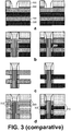
- Each semiconductor sub-device comprises a fin structure, consisting of alternating layers of Si (200) and Si 0.7 Ge 0.3 (100) for forming nanowires, a dummy gate comprising a dummy gate dielectric (300) and a dummy gate contact (400), and spacers (500).
- FIG. 3b An opening is made in the alternating layers between the spacers (500) and internal spacers (610, 620) are formed, before filling the opening with a source or drain contact (700) and capping (800) the source or drain contact (700) with a dielectric. Only one source or drain contact (700) is depicted per sub-device; the second contact, needed to from a field effect transistor (FET), is not depicted.
- FET field effect transistor
- internal spacers (610) are made at the level of the Si 0.7 Ge 0.3 layers (100) for the left sub-device, while internal spacers (620) are made at the level of the Si layers (200) for the right sub-device; however, no satisfactory solution is currently known for making these different internal spacers (610, 620). No such process for forming such SiGe internal spacers exists when starting from a Si/SiGe multilayer. Indeed, the internal spacer (610, 620) formation for the SiGe layers starting from a Si/SiGe stack requires an oxidation or deposition process which is selective toward Si with respect to SiGe. No such process is currently available.
- this internal spacer (610, 620) formation further requires a selective etching of Si with respect to SiGe.
- Existing selective methods of this kind are not satisfactory because the Si plane with miller indices (111) has an etch rate which is similar to the etch rate of SiGe.
- the dummy gate (300, 400) is removed and the Si 0.7 Ge 0.3 layers (100) or Si layers (200) are selectively removed (e.g. etched) with respect to one another: the Si 0.7 Ge 0.3 layers (100) for the left sub-device and the Si layers (200) for the right sub-device; leaving Si nanowires (200) for the left sub-device and Si 0.7 Ge 0.3 nanowires (100) for the right sub-device.
- a gate-all-around is formed around the Si nanowires (200) and Si 0.7 Ge 0.3 nanowires (100), comprising a gate dielectric (310) and a gate contact (410).
- the Si nanowires (200) and Si 0.7 Ge 0.3 nanowires (100) are each present at a different height, i.e. different distances from the substrate, which may result in undesired differences in sub-device performance.
- the gate has a different height in the left sub-device than in the right sub-device, which will make the contact module more difficult.
- Example 2 Integrating a Si 1-x Ge x nanowire FET with a Si 1-x' Ge x' nanowire FET, according to the present invention
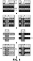
- Each semiconductor sub-device comprises a fin structure, consisting of alternating layers of Si 1-x Ge x (200, e.g. Si) and Si 1-z Ge z (100, z ⁇ 1 e.g. Si 0.7 Ge 0.3 ) for forming nanowires, a dummy gate comprising a dummy gate dielectric (300) and a dummy gate contact (400), and spacers (500).
- FIG. 4b An opening is made in the alternating layers between two spacers (500) and internal spacers (610) are formed, before filling the opening with a source or drain contact (700) and capping (800) the source or drain contact (700) with a dielectric.
- a source or drain contact 700
- capping 800
- the source or drain contact 700
- dielectric a dielectric
- internal spacers (610) are made at the level of the Si 1-z Ge z layers (100) for both sub-devices; thereby avoiding the problem of having to make different internal spacers.
- only one source or drain contact (700) is depicted per sub-device; the second one source or drain contact, needed to from a field effect transistor (FET), is not depicted.
- FET field effect transistor
- Fig. 4c The dummy gate (300, 400) is removed and the Si 1-z Ge z layers (100) are selectively removed (e.g. etched) with respect to the Si 1-x Ge x layers (200); leaving Si 1-x Ge x layers (200) in both sub-devices.
- the Si 1-x Ge x nanowires (200) in the right sub-device are subsequently transformed into Si 1-x' Ge x' nanowires (110) as described in example 1.
- the Si 1-z Ge z layers (100) and the Si 1-x' Ge x' nanowires (110) need not have the same composition.
- the sacrificial material Si 1-z Ge z may be chosen in function of its selective removal with respect to Si 1-x Ge x , independent of the desired Si 1-x' Ge x' for the nanowires.
- a gate-all-around is formed around the Si 1-x Ge x nanowires (200) and Si 1-x' Ge x' nanowires (110), comprising a gate dielectric (310) and a gate contact (410).
- the Si 1-x Ge x nanowires (200) and Si 1-x' Ge x' nanowires (110) are both present at the same height, i.e. they are vertically aligned, thus avoiding the resulting undesired differences in sub-device performance.
- no specific Si 1-x' Ge x' internal spacer module is required and the gate has the same height for both the Si 1-x Ge x nanowires (200) and the Si 1-x' Ge x' nanowires (110).
- Example 3 Integrating a Si 1-x Ge x nanowire FET with a Si 1-x' Ge x' nanowire FET, using a dummy source/drain, according to the present invention.
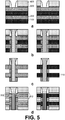
- Each semiconductor sub-device comprises a fin structure, consisting of alternating layers of Si 1-x Ge x (200, e.g. Si) and Si 1-z Ge z (100, e.g. Si 0.7 Ge 0.3 ) for forming nanowires, a dummy gate comprising a dummy gate dielectric (300) and a dummy gate contact (400), and spacers (500).
- FIG. 5b An opening is made in the alternating layers between two spacers (500) and internal spacers (610) are formed, before filling the opening with a dummy source or drain contact (710).
- internal spacers (610) are made at the level of the Si 1-z Ge zz layers (100) for both sub-devices; thereby avoiding the problem of having to make different internal spacers.
- source or drain contact (700) is depicted per sub-device; the second contact, needed to from a field effect transistor (FET), is not depicted.
- the dummy gate (300, 400) is removed and the Si 1-z Ge z layers (100) are selectively removed (e.g. etched) with respect to the Si 1-x Ge x layers (200); leaving Si 1-x Ge x nanowires (200) in both sub-devices.
- the Si 1-x Ge x nanowires (200) in the right sub-device are subsequently transformed into Si 1-x' Ge x' nanowires (110) as described in example 1.
- the Si 1-z Ge z layers (100) and the Si 1-x' Ge x' nanowires (110) need not have the same composition.
- the sacrificial material Si 1-z Ge z may be chosen in function of its selective removal with respect to Si 1-x Ge x , independent of the desired Si 1-x' Ge x' for the nanowires
- dummy source or drain contacts (710) are removed, before filling the opening with an actual source or drain contact (700) and capping (800) the source or drain contact (700) with a dielectric. Furthermore, a gate-all-around is formed around the Si 1-x Ge x nanowires (200) and Si 1-x' Ge x' nanowires (110), comprising a gate dielectric (310) and a gate contact (410). Note that, contrary to the comparative example, the Si 1-x Ge x nanowires (200) and Si 1-x' Ge x' nanowires (110) are both present at the same height, thus avoiding the resulting undesired differences in sub-device performance.
Landscapes
- Engineering & Computer Science (AREA)
- Chemical & Material Sciences (AREA)
- Nanotechnology (AREA)
- Crystallography & Structural Chemistry (AREA)
- Physics & Mathematics (AREA)
- Mathematical Physics (AREA)
- Theoretical Computer Science (AREA)
- Thin Film Transistor (AREA)
- Insulated Gate Type Field-Effect Transistor (AREA)
Abstract
In a first aspect, the present invention relates to a method for co-integrating Si 1-x Ge x structures (200) with Si 1-x' Ge x' structures (110) in a semiconductor device, comprising:
a. providing a device comprising a plurality of Si 1-x Ge x structures (200), wherein 0¤x<1,
b. depositing a layer of GeO 2 (250) on a subset of the Si 1-x Ge x structures (200), and
c. heating at least the subset of Si 1-x Ge x structures (200) at a temperature high enough and for a time long enough to transform the subset of Si 1-x Ge x structures (200) into a subset of Si 1-x' Ge x' structures (110) with x'>x.
Description
- The present invention relates to semiconductor devices and in particular to the integration of semiconductor structures of differing chemical natures in such devices.
- In the fabrication of semiconductor devices, it can be useful to cointegrate semiconductor structures comprising different semiconductor materials, such as different channel materials. However, this co-integration is typically difficult to achieve. A first issue may for example be due to difficulty in epitaxial growth of a first semiconductor material on a different semiconductor material. A further issue may also be the increased complexity of the device layout and its impact on several modules, e.g. separate internal spacer modules may be necessary for the different channel materials and making these is typically not trivial. An additional issue could also be the vertical misalignment between the different semiconductor materials, e.g. in the case where an alternating stack of Si and SiGe layers is formed, wherein alternatively Si and SiGe are selectively etched with respect to one another, the remaining Si and SiGe structures will be vertically displaced with respect to each other.
-
US9257450B2 - There is thus still a need in the art for methods and devices which improve some or all of these issues.
- It is an object of the present invention to provide good methods and devices for integrating semiconductor structures of differing chemical natures.
- It is an advantage of embodiments of the present invention that the integrated semiconductor structures differ in chemical composition, thereby enabling different sub-devices to be distinctively tuned (e.g. using different materials for n- and p-devices).
- It is an advantage of embodiments of the present invention that the chemical composition of the different semiconductor structures can be easily independently tuned with few or no integration problems.
- It is an advantage of embodiments of the present invention that there is no vertical displacement between corresponding semiconductor structures in different sub-devices within a same semiconductor device. The above objective is accomplished by a method and device according to the present invention.
- In a first aspect, the present invention relates to a method for integrating Si1-xGex structures with Si1-x'Gex' structures in a semiconductor device, comprising:
- a. providing a device comprising a plurality of Si1-xGex structures, wherein 0≤x<1,
- b. depositing a layer of GeO2 on a subset of the Si1-xGex structures, and
- c. heating at least the subset of Si1-xGex structures at a temperature high enough and for a time long enough to transform the subset of Si1-xGex structures into a subset of Si1-x'Gex' structures with x'>x.
- In a second aspect, the present invention relates to a semiconductor device, comprising
- i. a Si1-xGex structure with 0≤x<1, and
- ii. a Si1-x'Gex' structure with x<x'≤1, and
- iii. a Si1-yGeyO2 layer on the Si1-x'Gex' structure with 0<y<1.
- In a third aspect, the present invention relates to a semiconductor device comprising:
- a substrate having a top surface,
- a longitudinal Si1-xGex structure having a first longitudinal axis running parallel to the top surface of the substrate and separated therefrom by a non-null distance d,
- a longitudinal Si1-x'Gex' structure having a second longitudinal axis running parallel to the top surface of the substrate and separated therefrom by the non-null distance d so that both the first and the second longitudinal axis belong to a same plane parallel to the top surface of the substrate.
- Particular and preferred aspects of the invention are set out in the accompanying independent and dependent claims. Features from the dependent claims may be combined with features of the independent claims and with features of other dependent claims as appropriate and not merely as explicitly set out in the claims.
- Although there has been constant improvement, change and evolution of devices in this field, the present concepts are believed to represent substantial new and novel improvements, including departures from prior practices, resulting in the provision of more efficient, stable and reliable devices of this nature.
- The above and other characteristics, features and advantages of the present invention will become apparent from the following detailed description, taken in conjunction with the accompanying drawings, which illustrate, by way of example, the principles of the invention. This description is given for the sake of example only, without limiting the scope of the invention. The reference figures quoted below refer to the attached drawings.
-
-
Fig. 1 is a schematic representation of a method for transforming a Si1-xGex nanowire into a Si1-x'Gex' nanowire, according to an embodiment of the present invention. -
Fig. 2 is a flow chart showing the main steps in a method according to the present invention. -
Fig. 3 is a schematic representation of a method for integrating a Si1-xGex nanowire FET with a Si1-x'Gex' nanowire FET, without using the concepts of the present invention. -
Fig. 4 is a schematic representation of a method for integrating a Si1-xGex nanowire FET with a Si1-x'Gex' nanowire FET, according to an embodiment of the present invention. -
Fig. 5 is a schematic representation of a method for integrating a Si1-xGex nanowire FET with a Si1-x'Gex' nanowire FET, using a dummy source/drain, according to an embodiment of the present invention. - In the different figures, the same reference signs refer to the same or analogous elements.
- The present invention will be described with respect to particular embodiments and with reference to certain drawings but the invention is not limited thereto but only by the claims. The drawings described are only schematic and are non-limiting. In the drawings, the size of some of the elements may be exaggerated and not drawn on scale for illustrative purposes. The dimensions and the relative dimensions do not correspond to actual reductions to practice of the invention.
- Furthermore, the terms first, second, third and the like in the description and in the claims, are used for distinguishing between similar elements and not necessarily for describing a sequence, either temporally, spatially, in ranking or in any other manner. It is to be understood that the terms so used are interchangeable under appropriate circumstances and that the embodiments of the invention described herein are capable of operation in other sequences than described or illustrated herein.
- Moreover, the terms top, over, on and the like in the description and the claims are used for descriptive purposes and not necessarily for describing relative positions. It is to be understood that the terms so used are interchangeable with their antonyms (e.g. bottom, under, etc.) under appropriate circumstances and that the embodiments of the invention described herein are capable of operation in other orientations than described or illustrated herein.
- It is to be noticed that the term "comprising", used in the claims, should not be interpreted as being restricted to the means listed thereafter; it does not exclude other elements or steps. It is thus to be interpreted as specifying the presence of the stated features, integers, steps or components as referred to, but does not preclude the presence or addition of one or more other features, integers, steps or components, or groups thereof. Thus, the scope of the expression "a device comprising means A and B" should not be limited to devices consisting only of components A and B. It means that with respect to the present invention, the only relevant components of the device are A and B.
- Reference throughout this specification to "one embodiment" or "an embodiment" means that a particular feature, structure or characteristic described in connection with the embodiment is included in at least one embodiment of the present invention. Thus, appearances of the phrases "in one embodiment" or "in an embodiment" in various places throughout this specification are not necessarily all referring to the same embodiment, but may. Furthermore, the particular features, structures or characteristics may be combined in any suitable manner, as would be apparent to one of ordinary skill in the art from this disclosure, in one or more embodiments.
- Similarly, it should be appreciated that in the description of exemplary embodiments of the invention, various features of the invention are sometimes grouped together in a single embodiment, figure, or description thereof for the purpose of streamlining the disclosure and aiding in the understanding of one or more of the various inventive aspects. This method of disclosure, however, is not to be interpreted as reflecting an intention that the claimed invention requires more features than are expressly recited in each claim. Rather, as the following claims reflect, inventive aspects lie in less than all features of a single foregoing disclosed embodiment. Thus, the claims following the detailed description are hereby expressly incorporated into this detailed description, with each claim standing on its own as a separate embodiment of this invention.
- Furthermore, while some embodiments described herein include some but not other features included in other embodiments, combinations of features of different embodiments are meant to be within the scope of the invention, and form different embodiments, as would be understood by those in the art. For example, in the following claims, any of the claimed embodiments can be used in any combination.
- Furthermore, some of the embodiments are described herein as a method or combination of elements of a method that can be implemented by a processor of a computer system or by other means of carrying out the function. Thus, a processor with the necessary instructions for carrying out such a method or element of a method forms a means for carrying out the method or element of a method. Furthermore, an element described herein of an apparatus embodiment is an example of a means for carrying out the function performed by the element for the purpose of carrying out the invention.
- In the description provided herein, numerous specific details are set forth. However, it is understood that embodiments of the invention may be practiced without these specific details. In other instances, well-known methods, structures and techniques have not been shown in detail in order not to obscure an understanding of this description.
- The following terms are provided solely to aid in the understanding of the invention.
- As used herein, when a first material is said to be etched selectively with respect to a second material, this means that the first material is etched faster than the second material. Preferably, the etching process would etch the first material at least twice faster, or more preferably at least five times faster, yet more preferably at least 10 times faster, than the second material. In some preferred embodiments, the second material may be substantially not etched by the etching process.
- In a first aspect, the present invention relates to a method for integrating Si1-xGex structures with Si1-x'Gex' structures in a semiconductor device, comprising:
- a. providing a device comprising a plurality of Si1-xGex structures, wherein 0≤x<1,
- b. depositing a layer of GeO2 on a subset of the Si1-xGex structures, and
- c. heating at least the subset of Si1-xGex structures at a temperature high enough and for a time long enough to transform the subset of Si1-xGex structures into a subset of Si1-x'Gex' structures with x'>x. This first aspect is represented in the flowchart of
Fig. 2 . - The semiconductor device in the present invention typically comprises at least one sub-device, such as a transistor (e.g. a field effect transistor), preferably at least two sub-devices. In embodiments, one of the at least two sub-devices may comprise at least one of the Si1-xGex structures, while another of the at least two sub-devices may comprise at least one of the Si1-x'Gex' structures. In embodiments, a sub-device comprising at least one of the Si1-xGex structures may not comprise any Si1-x'Gex' structures. In embodiments, a sub-device comprising at least one of the Si1-x'Gex' structures may not comprise any Si1-xGex structures. In embodiments, the Si1-xGex and Si1-x'Gex' structures may be transistor channels.
- The Si1-xGex structures have a composition such that 0≤x<1. In embodiments, a Si1-xGex structure may be a SiGe or a Si structure. In embodiments, the Si1-xGex structures provided in step a may have at least one dimension equal to or smaller than 25 nm, preferably 15 nm, yet more preferably 10 nm. The at least one dimension may for example be a length, a width or a height of the structure. The at least one dimension is typically a width and/or height of the structure. In embodiments, the Si1-xGex structures provided in step a may be nanowires or nanosheets. In embodiments, the Si1-xGex structures may be nanowires having a width of from 3 to 20 nm, preferably 5 to 10 nm, and a height of from 3 to 20 nm, preferably 5 to 10 nm. The width and/or height of a nanowire, if it has a circular cross-section, are typically equal and may also be referred to as the diameter of the nanowire.
- The Si1-x'Gex' structures have a composition such that x'>x. x' may for example be from 0.05 to 1, preferably from 0.2 to 1. In embodiments, a Si1-x'Gex' structure may thus be a SiGe or a Ge structure. For instance, x may be 0 and x' may be from 0.25 to 0.45 or x may be from 0.50 to 0.70 and x' may be 1.
- Step b of depositing a layer of GeO2 on a subset of the Si1-xGex structures, may typically comprise masking the complementary subset of Si1-xGex structures which is not to be transformed into Si1-x'Gex' structures. For instance, a masking layer may be applied over the plurality of Si1-xGex structures and the mask may be opened above that subset which is to be transformed. It is clear to the person skilled in the art that this step could easily be repeated to achieve an integration of Si1-xGex, Si1-x'Gex', Si1-x"Gex", etc. structures (wherein x<x'<x", etc.).
- In embodiments, the layer of GeO2 in step b may be from 0.1 to 10 nm thick, preferably from 0.5 to 2.5 nm thick. The thickness of the layer of GeO2 typically plays a role in the composition (i.e. the value of x') of the Si1-x'Gex' structures that is obtained, wherein a thicker layer of GeO2 typically results in a higher Ge concentration (i.e. higher value of x'). In embodiments, step b may consist in depositing a conformal layer of GeO2 on the subset of the Si1-xGex structures. A conformal layer of GeO2 is advantageous because if step c is not performed long enough and/or at a temperature high enough to achieve a uniform chemical composition across the whole section of the structure, at least the chemical composition will be radially symmetrical. A radial symmetry of the nanowire chemical composition provides a core-shell type of structure where, band-offsets drive hole injection into the shell regions. Such radially symmetrical nanowires are also promising candidates for thermoelectric energy conversion. In embodiments, step b may be performed by atomic layer deposition. Atomic layer deposition advantageously allows the deposition of a conformal layer having a very uniform and well-defined thickness.
- Without being bound by theory, it is believed that heating the subset of Si1-xGex structures enables a reaction between GeO2 and Si1-xGex, thereby increasing the Ge concentration in the Si1-xGex:
GeO2 + Si1-xGex → GeSiO2 + Si1-x'Gex'.
In embodiments, step c may be performed at a temperature of at least 400 °C, preferably at least 500°C, more preferably at least 600°C, most preferably at least 750°C. In preferred embodiments, step c may be performed in the absence of a further compound able to oxidize the Si1-xGex structure. - In some embodiments, a Si1-x'Gex' structure may, during or after step c, have an inhomogeneous Ge concentration, such as a Ge concentration characterized by a spatial gradient. The Si1-x'Gex' structure may for example have a higher Ge concentration near a surface of the Si1-x'Gex' structure compared to a Ge concentration near a centre (i.e. away from the surface) of the Si1-x'Gex' structure.
- In some embodiments, there may exist a location in the Si1-x'Gex' structure obtained after step c, within 15 nm, preferably 10 nm, yet more preferably 5 nm of a surface of the Si1-x'Gex' structure, which has a Ge concentration at least 10% higher, preferably at least 20% higher, yet more preferably at least 30% higher, than at the corresponding location in the Si1-xGex structure obtained after step a. In some embodiments, there may exist a location in the Si1-x'Gex' structure obtained after step c, beyond 15 nm of any surface of the Si1-x'Gex' structure, which has a Ge concentration within 5%, preferably 2%, in absolute measure, than at the corresponding location in the Si1-xGex structure obtained after step a.
- In embodiments, step c may be performed for a time long enough (such as 1 hour or more) to entirely homogenize the chemical composition of at least one of the Si1-x'Gex' structures. In embodiments, step c may comprise heating the Si1-xGex structure to a temperature below the melting temperature of the Si1-xGex structure. Preferably, step c may comprise heating the Si1-xGex structure to a temperature below the melting temperature of the Si1-x'Gex' structure obtained in step c. For instance, step c may comprise heating the Si1-xGex structure to a temperature of 937 °C or below. A temperature of 937 °C or below is advantageously below the melting point of the Si1-x'Gex' structure since a temperature of 937°C is below the melting point of Ge. Performing step c at such a temperature advantageously avoids deterioration (such as changes in the geometric shape) of the Si1-x'Gex' structure due to melting.
- In embodiments, after completion of step c, the layer of GeO2 provided in step b may be removed after it has been transformed into a layer of Si1-yGeyO2 (with 0<y<1) during step c. Furthermore, after this removal, step b and step c may be repeated to further increase the Ge concentration (x') in the Si1-x'Gex' structure. In other embodiments, the layer of Si1-yGeyO2 (with 0<y<1) may be kept in place and serve as a passivation oxide.
- In embodiments, in step a, providing a plurality of Si1-xGex structures may comprise providing two or more fin structures, each fin structure comprising one or more Si1-xGex structures alternated with a sacrificial material, followed by selectively removing the sacrificial material with respect to the Si1-xGex structures. The sacrificial material may advantageously be of formula Si1-x'Gex' (see e.g. example 2 vs the comparative example). Furthermore, only one type of selective removal, i.e. of the sacrificial material with respect to the Si1-xGex structures, is performed; there is no need for two forms of selective removal with opposite selectivity (see e.g. example 2 vs the comparative example). In embodiments, the one or more Si1-xGex structures may be attached by their opposite ends to anchoring structures (e.g. source and drain contacts, dummy source and drain contacts, or internal spacers) and, after selectively removing the sacrificial material, the one or more Si1-xGex structures may remain suspended through said anchoring structures. In embodiments, an internal spacer may be provided at an end of the sacrificial material and selectively removing the sacrificial material may comprise removing the sacrificial material while preserving the internal spacer. It is an advantage of embodiments of the present invention that, when internal spacers are used, they can all be made of the same material (see e.g. example 2 vs. the comparative example).
- In embodiments, the method may further comprise after step c, forming a transistor, such as a field effect transistor (FET), by forming a gate covering part of the Si1-xGex structures or Si1-x'Gex' structures, thereby defining a channel in each of said parts, by forming a source and a drain region in the Si1-xGex structures or Si1-x'Gex' structure at opposite ends of each channel and by providing a source and a drain contact to the source and the drain region, respectively.
- In embodiments, forming a source and a drain contact may comprise a preliminary step, performed before step b, of providing a dummy source and a dummy drain contact, and subsequently, after step c, replacing the dummy source and the dummy drain contact by an actual conductive source and an actual conductive drain contact. The use of dummy source or drain contacts is advantageous when the thermal budget involved in step c would deteriorate the source or drain contacts. In this case, dummy source or drain contacts are used before and during step c and replaced after step c.
- In embodiments, forming a gate may comprise a preliminary step of providing a dummy gate during step a, and subsequently replacing the dummy gate by an actual gate after step c. In embodiments, the gate may comprise a gate dielectric (e.g. a high k dielectric) and a gate contact (e.g. Cu or W).
- The gate preferably surrounds the Si1-xGex or Si1-x'Gex' structure on all lateral sides. Within this context, a surface at a longitudinal end of the Si1-xGex or Si1-x'Gex' structure is thus not considered to be a lateral side. In other words, if the gate surrounds the Si1-xGex or Si1-x'Gex' structure on all lateral sides, a cross-section, perpendicular to the longitudinal axis, of the Si1-xGex or Si1-x'Gex' structure exists wherein the gate is in contact with the entire outer border of the Si1-xGex or Si1-x'Gex' structure in the cross-section. A gate surrounding the Si1-xGex or Si1-x'Gex' structure on all lateral sides may typically be referred to as a gate-all-around.
- In embodiments, when the Si1-xGex or Si1-x'Gex' structure is a cuboid, the gate may surround the Si1-xGex or Si1-x'Gex' structure on at least 3 lateral sides, preferably all lateral sides.
- In embodiments, when the Si1-xGex or Si1-x'Gex' structure has a circular cross-section taken perpendicularly to the length of the structure, the structure may have a single lateral side and the gate may surround the Si1-xGex or Si1-x'Gex' structure on this lateral side, i.e. on all lateral sides.
- In embodiments, transforming the subset of Si1-xGex structures into a subset of Si1-x'Gex' structures may comprise transforming the one or more Si1-xGex structures within at least one of the fin structures, while maintaining the one or more Si1-xGex structures within at least another of the fin structures.
- In a second aspect, the present invention relates to a semiconductor device, comprising
- i. a Si1-xGex structure with 0≤x<1, and
- ii. a Si1-x'Gex' structure with x<x'≤1, and
- iii. a Si1-yGeyO2 layer on the Si1-x'Gex' structure with 0<y<1.
- The semiconductor device according to the second aspect may be an intermediate in the fabrication of the semiconductor device of the third aspect.
- In preferred embodiments, y may be 0≤y<1, preferably 0.1≤y<1, yet more preferably 0.5≤y<1, such as 0.8≤y<1.
- In embodiments, the Si1-xGex structure and/or the Si1-x'Gex' structure may have at least one dimension equal to or smaller than 25 nm, preferably 15 nm, yet more preferably 10 nm. In embodiments, the Si1-xGex structure and/or the Si1-x'Gex' structure may be nanowires or nanosheets.
- In embodiments, the Ge concentration measured at the surface of the Si1-x'Gex' structure may be within 75%, preferably within 50%, more preferably within 30%, yet more preferably within 10%, and most preferably within 5%, of the Ge concentration at the centre of the Si1-x'Gex' structure.
- In embodiments, the Ge concentration measured at each location in the Si1-x'Gex' structure may be always within 75%, preferably within 50%, more preferably within 30%, yet more preferably within 10%, and most preferably within 5%, of the Ge concentration at any other location in the Si1-x'Gex' structure. For instance, if the largest discrepancy of concentration measurable within a Si1-x'Gex' structure is a measure of 80at% Ge at one location and 78at% at another location, it can be considered that the Ge concentration measured at each location in the Si1-x'Gex' structure will always be within 2.5% of the concentration at any other location in the Si1-x'Gex' structure. This is calculated from (80at%-78at%)/80at%=0.025 or 2.5%; we subtract the lower concentration from the highest concentration and we divide that difference by the highest concentration.
- In embodiments, the semiconductor device may further comprise:
- a gate covering part of the Si1-xGex structure or Si1-x'Gex' structure, thereby defining a channel in each of said parts,
- a source and a drain region in the Si1-xGex structure or Si1-x'Gex' structure at opposite ends of each channel,
- a source contact and a drain contact on the source region and the drain region respectively.
- In embodiments, the gate may surround the Si1-xGex or Si1-x'Gex' structure on at least 3 sides or on all sides.
- In embodiments, any feature of the second aspect or its embodiments may be as correspondingly described for the first aspect or the third aspect and its embodiments.
- In a third aspect, the present invention relates to a semiconductor device comprising:
- a substrate having a top surface,
- a longitudinal Si1-xGex structure having a first longitudinal axis running parallel to the top surface of the substrate and separated therefrom by a non-null distance d,
- a longitudinal Si1-x'Gex' structure having a second longitudinal axis running parallel to the top surface of the substrate and separated therefrom by the non-null distance d so that both the first and the second longitudinal axis belong to a same plane parallel to the top surface of the substrate.
- In embodiments, any feature of the third aspect or its embodiments may be as correspondingly described for the first or the second aspect and its embodiments.
- The invention will now be described by a detailed description of several embodiments of the invention. It is clear that other embodiments of the invention can be configured according to the knowledge of the person skilled in the art without departing from the true technical teaching of the invention, the invention being limited only by the terms of the appended claims.
- Reference will be made to transistors. These are devices typically having a first main electrode such as a drain, a second main electrode such as a source and a control electrode such as a gate for controlling the flow of electrical charges between the first and second main electrodes.
- It will be clear for a person skilled in the art that the present invention is also applicable to similar devices that can be configured in any transistor technology, including for example, but not limited thereto, CMOS, BICMOS, Bipolar and SiGe BICMOS technology.
- We now refer to
Fig. 1 . In the upper left, a cross-section is shown of a Si1-xGex nanowire (200) having a layer of GeO2 (250) therearound. Upon heating up the Si1-xGex nanowire (200), a reaction between the Si1-xGex and GeO2 occurs thereby exchanging Si atoms from the Si1-xGex with Ge atoms from the GeO2. - Depending on the circumstances, such as the temperature of heating and the dimensions of the nanowire, this action may directly result (solid arrow) in a Si1-x'Gex' nanowire (110), having a relatively uniform distribution of the Ge concentration, and a layer of Si1-yGeyO2 (260) with y<1 therearound.
- Under other circumstances, the reaction may in a first step (dashed arrow) be limited to an outer shell (210) of the nanowire, while a centre portion (220) of the nanowire may remain similar to the original Si1-xGex nanowire (200). A further step of homogenizing the outer shell (210) with the centre portion (220) may then be desired, typically achievable by further heating the nanowire (i.e. for a longer time and/or at a higher temperature).
- We now refer to
Fig. 3a . Two semiconductor sub-devices are schematically depicted in cross-section, which are typically present on a same substrate and will form part of a same semiconductor device. Each semiconductor sub-device comprises a fin structure, consisting of alternating layers of Si (200) and Si0.7Ge0.3 (100) for forming nanowires, a dummy gate comprising a dummy gate dielectric (300) and a dummy gate contact (400), and spacers (500). - We now refer to
Fig. 3b . An opening is made in the alternating layers between the spacers (500) and internal spacers (610, 620) are formed, before filling the opening with a source or drain contact (700) and capping (800) the source or drain contact (700) with a dielectric. Only one source or drain contact (700) is depicted per sub-device; the second contact, needed to from a field effect transistor (FET), is not depicted. Note that internal spacers (610) are made at the level of the Si0.7Ge0.3 layers (100) for the left sub-device, while internal spacers (620) are made at the level of the Si layers (200) for the right sub-device; however, no satisfactory solution is currently known for making these different internal spacers (610, 620). No such process for forming such SiGe internal spacers exists when starting from a Si/SiGe multilayer. Indeed, the internal spacer (610, 620) formation for the SiGe layers starting from a Si/SiGe stack requires an oxidation or deposition process which is selective toward Si with respect to SiGe. No such process is currently available. Furthermore, this internal spacer (610, 620) formation further requires a selective etching of Si with respect to SiGe. Existing selective methods of this kind are not satisfactory because the Si plane with miller indices (111) has an etch rate which is similar to the etch rate of SiGe. - We now refer to
Fig. 3c . The dummy gate (300, 400) is removed and the Si0.7Ge0.3 layers (100) or Si layers (200) are selectively removed (e.g. etched) with respect to one another: the Si0.7Ge0.3 layers (100) for the left sub-device and the Si layers (200) for the right sub-device; leaving Si nanowires (200) for the left sub-device and Si0.7Ge0.3 nanowires (100) for the right sub-device. This means that different selective etch processes with the opposite selectivity must exist, which is not trivial. - We now refer to
Fig. 3d . A gate-all-around is formed around the Si nanowires (200) and Si0.7Ge0.3 nanowires (100), comprising a gate dielectric (310) and a gate contact (410). Note that the Si nanowires (200) and Si0.7Ge0.3 nanowires (100) are each present at a different height, i.e. different distances from the substrate, which may result in undesired differences in sub-device performance. Furthermore, the gate has a different height in the left sub-device than in the right sub-device, which will make the contact module more difficult. - We now refer to
Fig. 4a . Two semiconductor sub-devices are schematically depicted in cross-sections taken perpendicularly to the width of a fin structure and parallel to its longitudinal axis. The two semiconductor sub-devices are typically present on a same substrate (not depicted). Each semiconductor sub-device comprises a fin structure, consisting of alternating layers of Si1-xGex (200, e.g. Si) and Si1-zGez (100, z≤1 e.g. Si0.7Ge0.3) for forming nanowires, a dummy gate comprising a dummy gate dielectric (300) and a dummy gate contact (400), and spacers (500). - We now refer to
Fig. 4b . An opening is made in the alternating layers between two spacers (500) and internal spacers (610) are formed, before filling the opening with a source or drain contact (700) and capping (800) the source or drain contact (700) with a dielectric. Note that, contrary to the comparative example, internal spacers (610) are made at the level of the Si1-zGez layers (100) for both sub-devices; thereby avoiding the problem of having to make different internal spacers. Further note that only one source or drain contact (700) is depicted per sub-device; the second one source or drain contact, needed to from a field effect transistor (FET), is not depicted. - We now refer to
Fig. 4c . The dummy gate (300, 400) is removed and the Si1-zGez layers (100) are selectively removed (e.g. etched) with respect to the Si1-xGex layers (200); leaving Si1-xGex layers (200) in both sub-devices. We can call the remaining layers, "nanowires". The Si1-xGex nanowires (200) in the right sub-device are subsequently transformed into Si1-x'Gex' nanowires (110) as described in example 1. Note that, contrary to the comparative example, the Si1-zGez layers (100) and the Si1-x'Gex' nanowires (110) need not have the same composition. As such, the sacrificial material Si1-zGez may be chosen in function of its selective removal with respect to Si1-xGex, independent of the desired Si1-x'Gex' for the nanowires. - We now refer to
Fig. 4d . A gate-all-around is formed around the Si1-xGex nanowires (200) and Si1-x'Gex' nanowires (110), comprising a gate dielectric (310) and a gate contact (410). Note that, contrary to the comparative example, the Si1-xGex nanowires (200) and Si1-x'Gex' nanowires (110) are both present at the same height, i.e. they are vertically aligned, thus avoiding the resulting undesired differences in sub-device performance. Also, no specific Si1-x'Gex' internal spacer module is required and the gate has the same height for both the Si1-xGex nanowires (200) and the Si1-x'Gex' nanowires (110). - We now refer to
Fig. 5a . Two semiconductor sub-devices are schematically depicted, which are typically present on a same substrate. Each semiconductor sub-device comprises a fin structure, consisting of alternating layers of Si1-xGex (200, e.g. Si) and Si1-zGez (100, e.g. Si0.7Ge0.3) for forming nanowires, a dummy gate comprising a dummy gate dielectric (300) and a dummy gate contact (400), and spacers (500). - We now refer to
Fig. 5b . An opening is made in the alternating layers between two spacers (500) and internal spacers (610) are formed, before filling the opening with a dummy source or drain contact (710). Note that, contrary to the comparative example, internal spacers (610) are made at the level of the Si1-zGezz layers (100) for both sub-devices; thereby avoiding the problem of having to make different internal spacers. Further note that only one source or drain contact (700) is depicted per sub-device; the second contact, needed to from a field effect transistor (FET), is not depicted. - We now refer to
Fig. 5c . The dummy gate (300, 400) is removed and the Si1-zGez layers (100) are selectively removed (e.g. etched) with respect to the Si1-xGex layers (200); leaving Si1-xGex nanowires (200) in both sub-devices. The Si1-xGex nanowires (200) in the right sub-device are subsequently transformed into Si1-x'Gex' nanowires (110) as described in example 1. Note that, contrary to the comparative example, the Si1-zGez layers (100) and the Si1-x'Gex' nanowires (110) need not have the same composition. As such, the sacrificial material Si1-zGez may be chosen in function of its selective removal with respect to Si1-xGex, independent of the desired Si1-x'Gex' for the nanowires - We now refer to
Fig. 5d . The dummy source or drain contacts (710) are removed, before filling the opening with an actual source or drain contact (700) and capping (800) the source or drain contact (700) with a dielectric. Furthermore, a gate-all-around is formed around the Si1-xGex nanowires (200) and Si1-x'Gex' nanowires (110), comprising a gate dielectric (310) and a gate contact (410). Note that, contrary to the comparative example, the Si1-xGex nanowires (200) and Si1-x'Gex' nanowires (110) are both present at the same height, thus avoiding the resulting undesired differences in sub-device performance. - It is to be understood that although preferred embodiments, specific constructions and configurations, as well as materials, have been discussed herein for devices according to the present invention, various changes or modifications in form and detail may be made without departing from the scope and technical teachings of this invention. For example, any formulas given above are merely representative of procedures that may be used. Functionality may be added or deleted from the block diagrams and operations may be interchanged among functional blocks. Steps may be added or deleted to methods described within the scope of the present invention.
Claims (15)
- A method for integrating Si1-xGex structures (200) with Si1-x'Gex' structures (110) in a semiconductor device, comprising:a. providing a device comprising a plurality of Si1-xGex structures (200), wherein 0≤x<1,b. depositing a layer of GeO2 (250) on a subset of the Si1-xGex structures (200), andc. heating at least the subset of Si1-xGex structures (200) at a temperature high enough and for a time long enough to transform the subset of Si1-xGex structures (200) into a subset of Si1-x'Gex' structures (110) with x'>x.
- The method according to claim 1, wherein the Si1-xGex structures (200) provided in step a have at least one dimension equal to or smaller than 25 nm, preferably 15 nm, yet more preferably 10 nm.
- The method according to claim 1 or 2, wherein the Si1-xGex structures (200) provided in step a are nanowires or nanosheets.
- The method according to any of the previous claims, wherein step b consists in depositing a conformal layer of GeO2 (250) on the subset of the Si1-xGex structures (200).
- The method according to any of the previous claims, wherein step c is performed at a temperature of at least 400 °C and at most 950°C.
- The method according to any of the previous claims, wherein step c is performed for a time long enough to homogenize the chemical composition of at least one of the Si1-x'Gex' structures (110).
- The method according to any of the previous claims, wherein, prior to step b, two or more fin structures are present in the device, the fin structures comprising one or more Si1-xGex structures (200) alternated with a sacrificial material (100).
- The method according to claim 7, further comprising selectively removing the sacrificial material (100) with respect to the Si1-xGex structures (200).
- The method according to claim 7 or 8, further comprising forming a transistor comprising two source or drain contacts (700) on opposite ends of one of the Si1-xGex (200) or Si1-x'Gex' (110) structures and a gate (310,410), thereby defining a channel in the Si1-xGex (200) or Si1-x'Gex' (110) structure.
- The method according to any of claims 7 to 9, wherein transforming the subset of Si1-xGex structures (200) into a subset of Si1-x'Gex' structures (110) comprises transforming the one or more Si1-xGex structures (200) within at least one of the fin structures, while maintaining the one or more Si1-xGex structures (200) within at least another of the fin structures.
- A semiconductor device comprising:- a substrate having a top surface,- a longitudinal Si1-xGex structure (200) having a first longitudinal axis running parallel to the top surface of the substrate and separated therefrom by a non-null distance d,- a longitudinal Si1-x'Gex' structure (110) having a second longitudinal axis running parallel to the top surface of the substrate and separated therefrom by the non-null distance d so that both the first and the second longitudinal axis belong to a same plane parallel to the top surface of the substrate.
- The semiconductor device according to claim 11, wherein the Si1-xGex structure (200) and/or the Si1-x'Gex' structure (110) have at least one dimension equal to or smaller than 25 nm, preferably 15 nm, yet more preferably 10 nm.
- The semiconductor device according to claim 11 or 12, wherein the Si1-xGex structure (200) and/or the Si1-x'Gex' structure (110) are nanowires or nanosheets.
- The semiconductor device according to any of claims 11 to 13, wherein the Ge concentration at each location in the Si1-x'Gex' structure (110) is always within 10%, preferably within 5%, of the Ge concentration at any other location in the Si1-x'Gex' structure.
- The semiconductor device according to any of claims 11 to 14, further comprising:- a gate (310, 410) covering part of the Si1-xGex structure (200) or Si1-x'Gex' structure (110), thereby defining a channel in each of said parts,- a source and a drain region in the Si1-xGex structure (200) or Si1-x'Gex' structure (210) at opposite ends of each channel, and- a source contact (700) and a drain contact (700) on the source region and the drain region respectively.
Priority Applications (3)
| Application Number | Priority Date | Filing Date | Title |
|---|---|---|---|
| EP17163709.3A EP3382761A1 (en) | 2017-03-29 | 2017-03-29 | Integration of silicon-germanium semiconductor structures |
| US15/913,546 US10515855B2 (en) | 2017-03-29 | 2018-03-06 | Integration of semiconductor structures |
| CN201810264539.6A CN108695252B (en) | 2017-03-29 | 2018-03-28 | Integration of semiconductor structures |
Applications Claiming Priority (1)
| Application Number | Priority Date | Filing Date | Title |
|---|---|---|---|
| EP17163709.3A EP3382761A1 (en) | 2017-03-29 | 2017-03-29 | Integration of silicon-germanium semiconductor structures |
Publications (1)
| Publication Number | Publication Date |
|---|---|
| EP3382761A1 true EP3382761A1 (en) | 2018-10-03 |
Family
ID=58464268
Family Applications (1)
| Application Number | Title | Priority Date | Filing Date |
|---|---|---|---|
| EP17163709.3A Withdrawn EP3382761A1 (en) | 2017-03-29 | 2017-03-29 | Integration of silicon-germanium semiconductor structures |
Country Status (3)
| Country | Link |
|---|---|
| US (1) | US10515855B2 (en) |
| EP (1) | EP3382761A1 (en) |
| CN (1) | CN108695252B (en) |
Cited By (1)
| Publication number | Priority date | Publication date | Assignee | Title |
|---|---|---|---|---|
| WO2021076241A1 (en) * | 2019-10-16 | 2021-04-22 | Qualcomm Incorporated | FIELD EFFECT TRANSISTOR (FET) COMPRISING CHANNELS WITH SILICON GERMANIUM (SiGe) |
Families Citing this family (1)
| Publication number | Priority date | Publication date | Assignee | Title |
|---|---|---|---|---|
| US10644138B2 (en) * | 2018-08-14 | 2020-05-05 | International Business Machines Corporation | Fin field-effect transistors with enhanced strain and reduced parasitic capacitance |
Citations (8)
| Publication number | Priority date | Publication date | Assignee | Title |
|---|---|---|---|---|
| US20090090934A1 (en) * | 2007-10-05 | 2009-04-09 | Tsutomu Tezuka | Field Effect Transistor and Method for Manufacturing the Same |
| US20110147811A1 (en) * | 2009-12-23 | 2011-06-23 | Kavalieros Jack T | Two-dimensional condensation for uniaxially strained semiconductor fins |
| US20110193178A1 (en) * | 2010-02-09 | 2011-08-11 | Taiwan Semiconductor Manufacturing Company, Ltd. | Bottom-Notched SiGe FinFET Formation Using Condensation |
| US20140065841A1 (en) * | 2012-09-05 | 2014-03-06 | Asm Ip Holding B.V. | ATOMIC LAYER DEPOSITION OF GeO2 |
| US9257450B2 (en) | 2014-02-18 | 2016-02-09 | Stmicroelectronics, Inc. | Semiconductor device including groups of stacked nanowires and related methods |
| US20160233303A1 (en) * | 2015-02-06 | 2016-08-11 | United Microelectronics Corp. | Semiconductor structure and manufacturing methods thereof |
| US20170005169A1 (en) * | 2015-06-30 | 2017-01-05 | Stmicroelectronics, Inc. | Method of using a sacrifical gate structure to make a metal gate finfet transistor |
| US20170040465A1 (en) * | 2015-08-04 | 2017-02-09 | United Microelectronics Corp. | Method of forming semiconductor device |
Family Cites Families (11)
| Publication number | Priority date | Publication date | Assignee | Title |
|---|---|---|---|---|
| US8020805B2 (en) | 2006-07-31 | 2011-09-20 | The United States Of America As Represented By The Administrator Of The National Aeronautics And Space Administration | High altitude airship configuration and power technology and method for operation of same |
| US8652891B1 (en) | 2012-07-25 | 2014-02-18 | The Institute of Microelectronics Chinese Academy of Science | Semiconductor device and method of manufacturing the same |
| CN103579295B (en) | 2012-07-25 | 2016-12-28 | 中国科学院微电子研究所 | Semiconductor device and manufacturing method thereof |
| US9041106B2 (en) * | 2012-09-27 | 2015-05-26 | Intel Corporation | Three-dimensional germanium-based semiconductor devices formed on globally or locally isolated substrates |
| US8765563B2 (en) | 2012-09-28 | 2014-07-01 | Intel Corporation | Trench confined epitaxially grown device layer(s) |
| US9431539B2 (en) * | 2014-10-10 | 2016-08-30 | Globalfoundries Inc. | Dual-strained nanowire and FinFET devices with dielectric isolation |
| US9716142B2 (en) | 2015-10-12 | 2017-07-25 | International Business Machines Corporation | Stacked nanowires |
| KR102557215B1 (en) | 2015-10-30 | 2023-07-18 | 유니버시티 오브 플로리다 리서치 파운데이션, 인크. | Encapsulated nanostructures and manufacturing methods |
| US9905672B2 (en) * | 2016-05-23 | 2018-02-27 | Samsung Electronics Co., Ltd. | Method of forming internal dielectric spacers for horizontal nanosheet FET architectures |
| US10079233B2 (en) * | 2016-09-28 | 2018-09-18 | International Business Machines Corporation | Semiconductor device and method of forming the semiconductor device |
| US9984940B1 (en) | 2017-01-30 | 2018-05-29 | International Business Machines Corporation | Selective and conformal passivation layer for 3D high-mobility channel devices |
-
2017
- 2017-03-29 EP EP17163709.3A patent/EP3382761A1/en not_active Withdrawn
-
2018
- 2018-03-06 US US15/913,546 patent/US10515855B2/en active Active
- 2018-03-28 CN CN201810264539.6A patent/CN108695252B/en active Active
Patent Citations (8)
| Publication number | Priority date | Publication date | Assignee | Title |
|---|---|---|---|---|
| US20090090934A1 (en) * | 2007-10-05 | 2009-04-09 | Tsutomu Tezuka | Field Effect Transistor and Method for Manufacturing the Same |
| US20110147811A1 (en) * | 2009-12-23 | 2011-06-23 | Kavalieros Jack T | Two-dimensional condensation for uniaxially strained semiconductor fins |
| US20110193178A1 (en) * | 2010-02-09 | 2011-08-11 | Taiwan Semiconductor Manufacturing Company, Ltd. | Bottom-Notched SiGe FinFET Formation Using Condensation |
| US20140065841A1 (en) * | 2012-09-05 | 2014-03-06 | Asm Ip Holding B.V. | ATOMIC LAYER DEPOSITION OF GeO2 |
| US9257450B2 (en) | 2014-02-18 | 2016-02-09 | Stmicroelectronics, Inc. | Semiconductor device including groups of stacked nanowires and related methods |
| US20160233303A1 (en) * | 2015-02-06 | 2016-08-11 | United Microelectronics Corp. | Semiconductor structure and manufacturing methods thereof |
| US20170005169A1 (en) * | 2015-06-30 | 2017-01-05 | Stmicroelectronics, Inc. | Method of using a sacrifical gate structure to make a metal gate finfet transistor |
| US20170040465A1 (en) * | 2015-08-04 | 2017-02-09 | United Microelectronics Corp. | Method of forming semiconductor device |
Cited By (1)
| Publication number | Priority date | Publication date | Assignee | Title |
|---|---|---|---|---|
| WO2021076241A1 (en) * | 2019-10-16 | 2021-04-22 | Qualcomm Incorporated | FIELD EFFECT TRANSISTOR (FET) COMPRISING CHANNELS WITH SILICON GERMANIUM (SiGe) |
Also Published As
| Publication number | Publication date |
|---|---|
| CN108695252A (en) | 2018-10-23 |
| US10515855B2 (en) | 2019-12-24 |
| US20180286762A1 (en) | 2018-10-04 |
| CN108695252B (en) | 2022-11-25 |
Similar Documents
| Publication | Publication Date | Title |
|---|---|---|
| US12237330B2 (en) | Architecture with stacked N and P transistors with a channel structure formed of nanowires | |
| US12027607B2 (en) | Methods for GAA I/O formation by selective epi regrowth | |
| US9589848B2 (en) | FinFET structures having silicon germanium and silicon channels | |
| US10707349B2 (en) | FinFETs with source/drain cladding | |
| US10008583B1 (en) | Gate-all-around nanosheet field-effect transistors and methods of manufacturing the same | |
| CN102956457B (en) | Semiconductor device structure and manufacturing method thereof, and semiconductor fin manufacturing method | |
| US9627377B2 (en) | Self-aligned dielectric isolation for FinFET devices | |
| US10141424B2 (en) | Method of producing a channel structure formed from a plurality of strained semiconductor bars | |
| US20130161756A1 (en) | Nanowire transistor devices and forming techniques | |
| CN109607475A (en) | Silicon and SiGe nanowire structure | |
| CN105280496A (en) | Semiconductor element with fin structure and manufacturing method thereof | |
| CN113284806B (en) | Ring gate device, source-drain preparation method thereof, device preparation method and electronic equipment | |
| US10515855B2 (en) | Integration of semiconductor structures | |
| US9620589B2 (en) | Integrated circuits and methods of fabrication thereof | |
| CN111799222A (en) | A method for forming a semiconductor device | |
| US11271091B2 (en) | Fin structure for vertical field effect transistor having two-dimensional shape in plan view | |
| WO2023035270A1 (en) | Preparation method for epitaxy of source/drain of gate all around structure, and gate all around structure | |
| US11088264B2 (en) | Self-aligned channel-only semiconductor-on-insulator field effect transistor | |
| CN113889413B (en) | Ring gate device, source-drain preparation method thereof, device preparation method and electronic equipment | |
| CN104795330B (en) | Semiconductor device and manufacturing method thereof | |
| WO2023035269A1 (en) | Gate-all-around device and source/drain preparation method therefor, device preparation method and electronic device | |
| CN114242594B (en) | Ring-gate device and its rear-gate single diffusion isolation process method and device preparation method | |
| CN109920738A (en) | Semiconductor structure and its production method | |
| CN104576366B (en) | Multi-gated transistor and preparation method thereof | |
| US20250120112A1 (en) | Semiconductor structure for gate all around nanosheet device |
Legal Events
| Date | Code | Title | Description |
|---|---|---|---|
| PUAI | Public reference made under article 153(3) epc to a published international application that has entered the european phase |
Free format text: ORIGINAL CODE: 0009012 |
|
| STAA | Information on the status of an ep patent application or granted ep patent |
Free format text: STATUS: THE APPLICATION HAS BEEN PUBLISHED |
|
| AK | Designated contracting states |
Kind code of ref document: A1 Designated state(s): AL AT BE BG CH CY CZ DE DK EE ES FI FR GB GR HR HU IE IS IT LI LT LU LV MC MK MT NL NO PL PT RO RS SE SI SK SM TR |
|
| AX | Request for extension of the european patent |
Extension state: BA ME |
|
| STAA | Information on the status of an ep patent application or granted ep patent |
Free format text: STATUS: THE APPLICATION IS DEEMED TO BE WITHDRAWN |
|
| 18D | Application deemed to be withdrawn |
Effective date: 20190404 |