EP3382758A1 - Electrostatic discharge (esd) protection device and method for operating an esd protection device - Google Patents
Electrostatic discharge (esd) protection device and method for operating an esd protection device Download PDFInfo
- Publication number
- EP3382758A1 EP3382758A1 EP18157430.2A EP18157430A EP3382758A1 EP 3382758 A1 EP3382758 A1 EP 3382758A1 EP 18157430 A EP18157430 A EP 18157430A EP 3382758 A1 EP3382758 A1 EP 3382758A1
- Authority
- EP
- European Patent Office
- Prior art keywords
- esd
- protection device
- nmos transistor
- esd protection
- bigfet
- Prior art date
- Legal status (The legal status is an assumption and is not a legal conclusion. Google has not performed a legal analysis and makes no representation as to the accuracy of the status listed.)
- Granted
Links
Images



Classifications
-
- H—ELECTRICITY
- H10—SEMICONDUCTOR DEVICES; ELECTRIC SOLID-STATE DEVICES NOT OTHERWISE PROVIDED FOR
- H10W—GENERIC PACKAGES, INTERCONNECTIONS, CONNECTORS OR OTHER CONSTRUCTIONAL DETAILS OF DEVICES COVERED BY CLASS H10
- H10W42/00—Arrangements for protection of devices
- H10W42/60—Arrangements for protection of devices protecting against electrostatic charges or discharges, e.g. Faraday shields
-
- H—ELECTRICITY
- H02—GENERATION; CONVERSION OR DISTRIBUTION OF ELECTRIC POWER
- H02H—EMERGENCY PROTECTIVE CIRCUIT ARRANGEMENTS
- H02H9/00—Emergency protective circuit arrangements for limiting excess current or voltage without disconnection
- H02H9/04—Emergency protective circuit arrangements for limiting excess current or voltage without disconnection responsive to excess voltage
-
- H—ELECTRICITY
- H02—GENERATION; CONVERSION OR DISTRIBUTION OF ELECTRIC POWER
- H02H—EMERGENCY PROTECTIVE CIRCUIT ARRANGEMENTS
- H02H9/00—Emergency protective circuit arrangements for limiting excess current or voltage without disconnection
- H02H9/04—Emergency protective circuit arrangements for limiting excess current or voltage without disconnection responsive to excess voltage
- H02H9/045—Emergency protective circuit arrangements for limiting excess current or voltage without disconnection responsive to excess voltage adapted to a particular application and not provided for elsewhere
- H02H9/046—Emergency protective circuit arrangements for limiting excess current or voltage without disconnection responsive to excess voltage adapted to a particular application and not provided for elsewhere responsive to excess voltage appearing at terminals of integrated circuits
-
- H—ELECTRICITY
- H03—ELECTRONIC CIRCUITRY
- H03K—PULSE TECHNIQUE
- H03K19/00—Logic circuits, i.e. having at least two inputs acting on one output; Inverting circuits
- H03K19/003—Modifications for increasing the reliability for protection
- H03K19/00315—Modifications for increasing the reliability for protection in field-effect transistor circuits
-
- H—ELECTRICITY
- H10—SEMICONDUCTOR DEVICES; ELECTRIC SOLID-STATE DEVICES NOT OTHERWISE PROVIDED FOR
- H10D—INORGANIC ELECTRIC SEMICONDUCTOR DEVICES
- H10D1/00—Resistors, capacitors or inductors
- H10D1/40—Resistors
- H10D1/47—Resistors having no potential barriers
-
- H—ELECTRICITY
- H10—SEMICONDUCTOR DEVICES; ELECTRIC SOLID-STATE DEVICES NOT OTHERWISE PROVIDED FOR
- H10D—INORGANIC ELECTRIC SEMICONDUCTOR DEVICES
- H10D1/00—Resistors, capacitors or inductors
- H10D1/60—Capacitors
- H10D1/68—Capacitors having no potential barriers
-
- H—ELECTRICITY
- H10—SEMICONDUCTOR DEVICES; ELECTRIC SOLID-STATE DEVICES NOT OTHERWISE PROVIDED FOR
- H10D—INORGANIC ELECTRIC SEMICONDUCTOR DEVICES
- H10D84/00—Integrated devices formed in or on semiconductor substrates that comprise only semiconducting layers, e.g. on Si wafers or on GaAs-on-Si wafers
- H10D84/80—Integrated devices formed in or on semiconductor substrates that comprise only semiconducting layers, e.g. on Si wafers or on GaAs-on-Si wafers characterised by the integration of at least one component covered by groups H10D12/00 or H10D30/00, e.g. integration of IGFETs
- H10D84/811—Combinations of field-effect devices and one or more diodes, capacitors or resistors
-
- H—ELECTRICITY
- H10—SEMICONDUCTOR DEVICES; ELECTRIC SOLID-STATE DEVICES NOT OTHERWISE PROVIDED FOR
- H10D—INORGANIC ELECTRIC SEMICONDUCTOR DEVICES
- H10D84/00—Integrated devices formed in or on semiconductor substrates that comprise only semiconducting layers, e.g. on Si wafers or on GaAs-on-Si wafers
- H10D84/80—Integrated devices formed in or on semiconductor substrates that comprise only semiconducting layers, e.g. on Si wafers or on GaAs-on-Si wafers characterised by the integration of at least one component covered by groups H10D12/00 or H10D30/00, e.g. integration of IGFETs
- H10D84/811—Combinations of field-effect devices and one or more diodes, capacitors or resistors
- H10D84/813—Combinations of field-effect devices and capacitor only
-
- H—ELECTRICITY
- H10—SEMICONDUCTOR DEVICES; ELECTRIC SOLID-STATE DEVICES NOT OTHERWISE PROVIDED FOR
- H10D—INORGANIC ELECTRIC SEMICONDUCTOR DEVICES
- H10D84/00—Integrated devices formed in or on semiconductor substrates that comprise only semiconducting layers, e.g. on Si wafers or on GaAs-on-Si wafers
- H10D84/80—Integrated devices formed in or on semiconductor substrates that comprise only semiconducting layers, e.g. on Si wafers or on GaAs-on-Si wafers characterised by the integration of at least one component covered by groups H10D12/00 or H10D30/00, e.g. integration of IGFETs
- H10D84/811—Combinations of field-effect devices and one or more diodes, capacitors or resistors
- H10D84/817—Combinations of field-effect devices and resistors only
-
- H—ELECTRICITY
- H10—SEMICONDUCTOR DEVICES; ELECTRIC SOLID-STATE DEVICES NOT OTHERWISE PROVIDED FOR
- H10D—INORGANIC ELECTRIC SEMICONDUCTOR DEVICES
- H10D89/00—Aspects of integrated devices not covered by groups H10D84/00 - H10D88/00
- H10D89/60—Integrated devices comprising arrangements for electrical or thermal protection, e.g. protection circuits against electrostatic discharge [ESD]
-
- H—ELECTRICITY
- H10—SEMICONDUCTOR DEVICES; ELECTRIC SOLID-STATE DEVICES NOT OTHERWISE PROVIDED FOR
- H10D—INORGANIC ELECTRIC SEMICONDUCTOR DEVICES
- H10D89/00—Aspects of integrated devices not covered by groups H10D84/00 - H10D88/00
- H10D89/60—Integrated devices comprising arrangements for electrical or thermal protection, e.g. protection circuits against electrostatic discharge [ESD]
- H10D89/601—Integrated devices comprising arrangements for electrical or thermal protection, e.g. protection circuits against electrostatic discharge [ESD] for devices having insulated gate electrodes, e.g. for IGFETs or IGBTs
- H10D89/811—Integrated devices comprising arrangements for electrical or thermal protection, e.g. protection circuits against electrostatic discharge [ESD] for devices having insulated gate electrodes, e.g. for IGFETs or IGBTs using FETs as protective elements
- H10D89/813—Integrated devices comprising arrangements for electrical or thermal protection, e.g. protection circuits against electrostatic discharge [ESD] for devices having insulated gate electrodes, e.g. for IGFETs or IGBTs using FETs as protective elements specially adapted to provide an electrical current path other than the field-effect induced current path
-
- H—ELECTRICITY
- H10—SEMICONDUCTOR DEVICES; ELECTRIC SOLID-STATE DEVICES NOT OTHERWISE PROVIDED FOR
- H10D—INORGANIC ELECTRIC SEMICONDUCTOR DEVICES
- H10D89/00—Aspects of integrated devices not covered by groups H10D84/00 - H10D88/00
- H10D89/60—Integrated devices comprising arrangements for electrical or thermal protection, e.g. protection circuits against electrostatic discharge [ESD]
- H10D89/601—Integrated devices comprising arrangements for electrical or thermal protection, e.g. protection circuits against electrostatic discharge [ESD] for devices having insulated gate electrodes, e.g. for IGFETs or IGBTs
- H10D89/811—Integrated devices comprising arrangements for electrical or thermal protection, e.g. protection circuits against electrostatic discharge [ESD] for devices having insulated gate electrodes, e.g. for IGFETs or IGBTs using FETs as protective elements
- H10D89/819—Bias arrangements for gate electrodes of FETs, e.g. RC networks or voltage partitioning circuits
-
- H—ELECTRICITY
- H10—SEMICONDUCTOR DEVICES; ELECTRIC SOLID-STATE DEVICES NOT OTHERWISE PROVIDED FOR
- H10P—GENERIC PROCESSES OR APPARATUS FOR THE MANUFACTURE OR TREATMENT OF DEVICES COVERED BY CLASS H10
- H10P95/00—Generic processes or apparatus for manufacture or treatments not covered by the other groups of this subclass
Definitions
- Embodiments of the invention relate generally to electronic hardware and methods for operating electronic hardware, and, more particularly, to electrostatic discharge (ESD) protection devices and methods for operating an ESD protection device.
- ESD electrostatic discharge
- An ESD protection device can be integrated into an integrated circuit (IC) chip to provide a low impedance channel to ground to protect against thermal damage in the IC substrate.
- IC integrated circuit
- an ESD protection device typically shunts a current pulse with a peak value of 1 or 2 ampere (A).
- IEC International Electrotechnical Commission
- a system-level ESD pulse or a part thereof is conducted through a conventional ESD protection device, there is a risk that the ESD protection device has to sink a significantly higher ESD current pulse than the device is designed to sink. This may result in physical damage to the ESD protection device itself, to the core circuit that is protected by the ESD protection device, or to both.
- an ESD protection device includes an NMOS transistor configured to shunt current in response to an ESD pulse and a bigFET connected in parallel with the NMOS transistor.
- the NMOS transistor includes a source terminal, a gate terminal, and a body. The gate terminal and the body of the NMOS transistor are connected to the source terminal via a resistor.
- Other embodiments are also described.
- the NMOS transistor and the bigFET are both connected between first and second nodes through which the ESD pulse is received.
- the NMOS transistor further includes a drain terminal connected to the first node, and the source terminal is connected to the second node.
- the resistor is connected to the second node.
- the ESD pulse includes a first current peak and a subsequent second current peak that is lower than the first current peak.
- the NMOS transistor is configured to shunt the current during the first peak of the ESD pulse.
- the bigFET is configured to conduct ESD current during the second peak of the ESD pulse.
- the NMOS transistor further includes a silicide block mask.
- the silicide block mask extends less than a predefined length from the gate terminal to a drain region of the NMOS transistor.
- the predefined length is 1 ⁇ m.
- the ESD protection device further includes a trigger device connected between the first and second nodes and configured to trigger a gate terminal of the bigFET in response to the ESD pulse.
- the ESD protection device further includes a decoupling capacitor connected in parallel with the NMOS transistor.
- an IC device includes the ESD protection device and a device to be protected connected in parallel with the ESD protection device.
- an ESD protection device includes an NMOS transistor configured to shunt current in response to an ESD pulse, a bigFET connected in parallel with the NMOS transistor, and a trigger device configured to trigger a gate terminal of the bigFET in response to the ESD pulse.
- the NMOS transistor includes a source terminal, a gate terminal and a body. The gate terminal and the body of the NMOS transistor are connected to the source terminal via a resistor. The source terminal and the resistor are connected to ground.
- the NMOS transistor and the bigFET are both connected between first and second nodes through which the ESD pulse is received.
- the NMOS transistor further includes a drain terminal connected to the first node.
- the source terminal is connected to the second node.
- the ESD pulse includes a first current peak and a subsequent second current peak that is lower than the first current peak.
- the NMOS transistor is configured to shunt the current during the first peak of the ESD pulse.
- the bigFET is configured to conduct ESD current during the second peak of the ESD pulse.
- the bigFET is configured to conduct ESD current during the second peak of the ESD pulse.
- the NMOS transistor further includes a silicide block mask.
- the silicide block mask extends less than a predefined length from the gate terminal to a drain region of the NMOS transistor.
- the predefined length is 1 ⁇ m.
- the ESD protection device further includes a decoupling capacitor connected in parallel with the NMOS transistor.
- a method for operating an ESD protection device conducting a first peak of an ESD pulse using an NMOS transistor of the ESD protection device and conducting a second peak of the ESD pulse using a bigFET of the ESD protection device that is connected in parallel with the NMOS transistor.
- Fig. 1 is a schematic block diagram of a circuit 120 in accordance with an embodiment of the invention.
- the circuit can be used in various applications, such as automotive applications, communications applications, industrial applications, medical applications, computer applications, and/or consumer or appliance applications.
- the circuit includes an IC device 100, which includes a core circuit 102 and an ESD protection device 104 that is used to protect the core circuit during an ESD event, which may be an ESD test or an actual ESD strike.
- the IC device can be implemented in a substrate, such as a semiconductor wafer or a printed circuit board (PCB).
- the IC device is packaged as a semiconductor IC chip.
- the IC device may be included in a microcontroller, which can be used for, for example, in vehicle control or communications, identification, wireless communications, and/or lighting control.
- the IC device is included in a computing device, such as a smartphone, a tablet computer, a laptop, etc.
- the IC device may be included in a Near Field Communications (NFC) capable computing device.
- NFC Near Field Communications
- the circuit is shown in Fig. 1 as including the core circuit and the ESD protection device, in other embodiments, the circuit may include additional circuit elements.
- the circuit may include a control circuit that is located in a low voltage domain and used to control the core circuit that is located in a high voltage domain.
- the core circuit and the ESD protection device are connected to first and second nodes 122, 124 through which an ESD pulse may be received.
- the first and second nodes may be coupled to different voltages.
- the first node 122 is connected to a positive voltage and the second node 124 is connected to the ground or a voltage that is lower than the voltage at the first node.
- the first and second nodes are electrical terminals of the IC device, such as electrical contact pads or electrical contact pins of the IC device.
- the core circuit 102 is a device to be protected by the ESD protection device 104 in case of an ESD event.
- the core circuit typically includes one or more internal circuit components that are susceptible to ESD strikes. Examples of the core circuit include, but are not limited to, microcontrollers, transceivers, and switching circuits.
- the core circuit includes a power supply domain of the IC device 100.
- the core circuit may be connected to a power supply rail 110 with a supply voltage, "V DD ,” of the IC device 100 and a voltage rail 140 with a lower voltage, "Vss.”
- the voltage rail 140 is connected to ground.
- the IC device is shown in Fig. 1 as including the core circuit and the ESD protection device 104, in other embodiments, the IC device may include additional circuit elements.
- the IC device may include serially connected diodes that are coupled in parallel with the core circuit for current restriction and voltage surge protection.
- the ESD protection device 104 protects the core circuit 102 during an ESD event.
- the ESD protection device can be used to protect a power supply domain of the IC device 100.
- the ESD protection device may be connected to the power supply rail, "V DD ,” of the IC device 100.
- the ESD protection device can be implemented by suitable semiconductor devices.
- the ESD protection device includes an NMOS transistor 112, a big field-effect transistor (bigFET) 106 connected in parallel with the NMOS transistor, and a trigger device 108.
- the ESD protection device is shown in Fig. 1 as including the bigFET, the trigger device, and the NMOS transistor, in other embodiments, the electrical device may include additional circuit elements.
- the ESD protection device may include one or more additional transistors and/or resistors.
- the NMOS transistor 112 of the ESD protection device 104 is configured to shunt current in response to an ESD pulse.
- the NMOS transistor includes a source terminal, "S,” a gate terminal, "G,” a body, "B,” 132, and a drain terminal, "D.”
- the gate terminal, G, and the body, B, of the NMOS transistor are connected to the source terminal, S, of the NMOS transistor via a resistor 134.
- the drain terminal, D, of the NMOS transistor is electrically connected to the first node 122 and the source terminal, S, of the NMOS transistor is electrically connected to the second node 124.
- the resistor may be also electrically connected to the second node.
- the source terminal, S, of the NMOS transistor and the resistor are connected to ground.
- the bigFET 106 of the ESD protection device 104 is configured to conduct current during an ESD event.
- the bigFET is an NMOS device (e.g., an NMOS transistor) with a large channel width to sink ESD current.
- a bigFET can be used to protect a power supply domain of the IC device 100 from overvoltage during an ESD event by shunting the ESD current from the power supply domain to the ground domain (i.e., the ground).
- the channel width of a bigFET can be chosen to ensure that the voltage drop across the bigFET during an ESD event does not exceed a predetermined voltage, which may be harmful to the inner circuit components (e.g., the core circuit 102) of the IC device.
- the channel width of the bigFET is chosen such that the ESD current caused by an ESD event flows through the bigFET while keeping the voltage drop generated across the bigFET below a pre-determined value, which can be set to a value between 50% and 150% of the nominal value of V DD .
- the predetermined voltage is typically set to be equal to or around (e.g., ⁇ 30%) the power supply voltage of the IC device.
- the ESD pulse includes a first current peak and a subsequent second current peak that is lower than the first current peak.
- the NMOS transistor is configured to shunt the current during the first peak of the ESD pulse while the bigFET is configured to conduct ESD current during the second peak of the ESD pulse.
- the trigger device 108 of the ESD protection device 104 is configured to detect an ESD event and to drive the bigFET 106 for a certain amount of time during an ESD event.
- the trigger device is connected between the first and second nodes 122, 124 and configured to trigger the gate terminal, "G," of the bigFET (e.g., by applying an appropriate voltage to the gate terminal, G, of the bigFET) in response to an ESD pulse.
- the trigger device can be implemented using one or more capacitors, transistors, and/or resistors.
- the trigger device is similar to or the same as trigger devices described in U.S. Patent No.
- the trigger device 108 includes a slew rate detector, an optional pre-driver stage, a keep-on latch, and a driver stage.
- the trigger device may include more or less components to implement more or less functionalities.
- the slew rate detector is a circuit that is configured to detect an ESD event, which may be an ESD test or an actual ESD strike, for example, by detecting a rise in the power supply voltage, "V DD ,” of the IC device 100, which is characteristic of an ESD event.
- the pre-driver stage is a circuit that is configured to turn on the driver stage once an ESD event is detected by the slew rate detector.
- the pre-driver stage may only be active during the initial detection of an ESD event to "trigger" the driver stage.
- the keep-on latch is a circuit that is configured to keep the driver stage turned on for the expected maximum duration of the detected ESD event.
- the functions of the slew rate detector and the keep-on latch are implemented in a single circuit.
- the driver stage is a circuit that is configured to drive the gate terminal of the bigFET.
- a combination of the bigFET and the trigger device is referred to as a "railclamp.”.
- a railclamp can be used to protect a supply domain of an IC chip from overheating during an ESD strike by shunting the ESD current from the supply domain to the ground domain.
- a railclamp can also be used to protect non-supply pins such as inputs, outputs, or combined input/output pins (IOs).
- the circuit 120 includes a decoupling capacitor 114 located on a substrate 116, such as a Printed Circuit Board (PCB), of the circuit 120.
- the decoupling capacitor may be connected in parallel with the NMOS transistor.
- the decoupling capacitor is physically attached and in physical and electrical contact with the substrate.
- the primary purpose of the decoupling capacitor is to suppress ripple on the supply voltage during normal operation.
- the decoupling capacitor can be used with the ESD protection device 104 of the IC device 100 for robustness against system-level ESD pulses. For example, the ESD protection device inside the IC device shunts a small portion of the system-level ESD current, and the decoupling capacitor stores the rest of the ESD pulse at a voltage that is lower than the threshold voltage of the IC.
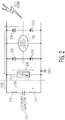
- Fig. 2 illustrates an example of ESD current paths through the ESD protection device 104 and the decoupling capacitor 114 of the circuit 120 during an ESD event.
- a dashed line separates elements on a substrate, such as a printed circuit board (PCB), with elements on an IC chip.
- the decoupling capacitor is located on one side of the substrate while the ESD protection device 104 and the core circuit 102 are located on the other side of the substrate.
- the ESD event may cause a system-level ESD pulse with a high peak current or a regular ESD pulse with a low peak current.
- serially connected diodes 224, 226 and 228, 230 are connected in parallel with the core circuit for current restriction and voltage surge protection purpose.
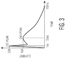
- Fig. 3 depicts an example of a system-level ESD pulse that can be conducted through the ESD current paths of Fig. 2 .
- the system-level ESD pulse includes a first current peak and a second current peak that is lower than the first current peak.
- the system-level ESD pulse may have a first peak of about 30 Ampere (A) occurring about 1 ns into the pulse, followed by a second peak of 16 A occurring at around 30 ns, and a duration of around 150 ns.
- A Ampere
- the decoupling capacitor 114 not only has a certain capacitance but also has some parasitic inductance represented as inductors 240, as shown in Fig. 2 .
- the consequence of the decoupling capacitor having both a capacitance and an inductance is that the decoupling capacitor may absorb only the second peak of a system-level ESD pulse (e.g., an IEC61000-4-2 pulse), as illustrated by arrow 238, and force the first peak of the system-level pulse through the ESD protection device 104 incorporated in the IC device 100, as illustrated by arrow 236.
- a bigFET based ESD protection device is typically designed to sink a current of a few Amperes (A).
- a first current peak of a system-level ESD pulse which may be as strong as 30 A, can damage the bigFET based ESD protection device and ruin the core circuit.
- the negative effect of the parasitic inductance of the decoupling capacitor can be addressed by placing tight constraints on the PCB design and choosing a capacitor with minimal parasitic inductance. For example, a smaller decoupling capacitor with a low value of parasitic inductance can be used in parallel with a main decoupling capacitor. However, two capacitors with different characteristics are more expensive than a one-capacitor solution. Alternatively, a capacitor with a relatively low inductance can be used as the decoupling capacitor.
- a capacitor with a relatively low inductance is more expensive to manufacture than a capacitor with higher inductance.
- a transient voltage suppressor TVS
- the addition of a TVS can lead to more stringent design constraints for the PCB layout and increased system cost.
- a TVS may not respond fast enough to fully protect against the first peak of a system-level ESD pulse.
- the NMOS transistor 112 handles the first peak of the system-level ESD pulse.
- the bigFET and the decoupling capacitor keep the voltage below the threshold voltage of the NMOS transistor as the bigFET and the decoupling capacitor sink or store the second peak current of the system-level ESD pulse. Consequently, the ESD protection device described with reference to Figs. 1 and 2 can be used with a decoupling capacitor with a relatively large inductance and the constraints that otherwise exist for the PCB design or the choice of capacitor types can be relaxed.
- the ESD protection device depicted in Fig. 1 can be used with the decoupling capacitor to form an economical and compact ESD protection network against system-level ESD pulses.
- the ESD protection device depicted in Fig. 1 allows the flexibility of choosing the location of the decoupling capacitor within the PCB layout.
- the decoupling capacitor can be placed close to the IC device 100 to be more effective at stabilizing the supply voltage.
- the ESD protection device depicted in Fig. 1 uses the NMOS transistor 112 to achieve faster ESD response time and to reduce substrate footprint.
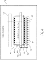
- Fig. 4 depicts a top layout view of an NMOS transistor 412 in accordance with an embodiment of the invention.
- the NMOS transistor includes drain contacts 442, an N+ drain region 444, a gate structure 446, an N+ source region 448, source contacts 450, a P-type body region 452, body contacts 454, and a resistor 434 connected to the gate structure, to the body contacts and to the source contacts.
- the NMOS transistor 412 depicted in Fig. 4 is a possible implementation of the NMOS transistor 112 depicted in Fig. 1 .
- the NMOS transistor 112 depicted in Fig. 1 can be implemented differently from the layout depicted in Fig. 4 .
- the NMOS transistor 412 is shown in Fig. 4 as including a certain number of N-doped sections and P-doped regions, in other embodiments, the NMOS transistor 412 may include more or less N-doped regions and/or P-doped regions.
- a silicide block mask 458 covers (e.g., on top of (e.g., in direct contact with)) the N+ drain region 444, the gate structure 446, and the N+ source region 448.
- the drain ballast resistance of the NMOS transistor 412 may be the equivalent resistance that electrical current encounters when it traverses from the P-type body region 452, through the N+ drain region, to the drain contacts 442.
- the purpose of having drain ballast resistance in NMOS transistors is to ensure homogeneous current flow within the NMOS transistor.
- the drain ballast resistance of the NMOS transistor 412 is a fraction of the drain ballast resistance of a conventional grounded gate NMOS transistor.
- the drain ballast resistance of the NMOS transistor 412 is about (e.g., ⁇ 5%) 1/3 or about (e.g., ⁇ 5%) 1/5 of the drain ballast resistance of a conventional grounded gate NMOS transistor.
- the drain ballast resistance of the NMOS transistor can be reduced by reducing the length that the silicide block mask 458 extends from the gate structure into the N+ drain region 444.
- the reduced drain ballast resistance can lead to a reduction in the voltage at which the NMOS transistor operates during an ESD event. Consequently, the NMOS transistor can provide more effective ESD protection.
- silicon area can be saved.
- the silicide block mask in a conventional NMOS transistor can extend over 3 ⁇ m from the edge of a gate structure into a drain region. Consequently, the size of the silicide block mask and the drain region and the size of the NMOS transistor can be reduced compared to a conventional grounded gate NMOS transistor.
- the P-type body region 452 of the NMOS transistor 412 is connected to the N+ source region 448 via the resistor 434.
- the source contacts 450 and the body contacts 454 are connected via the resistor.
- the resistance of the resistor can be set to various values.
- the resistor may have a resistance value of several k ⁇ .
- the resistor can promote ESD triggering in the NMOS transistor by the capacitive loading current of the internal body-drain capacitor, rather by impact ionization.
- the NMOS transistor should to be triggered homogeneously. Triggering by the loading current of the internal drain-body capacitor tends to be homogeneous across the NMOS transistor.
- Fig. 5 depicts a cross sectional view of the NMOS transistor 412 depicted in Fig. 4 at the location indicated in Fig. 4 by the dashed line 460.
- an isolated P-well region 562 is formed on top of (e.g., in direct contact with) a first N-well/deep N-well region 564.
- the first N-well/deep N-well region is formed on top of (e.g., in direct contact with) a P-doped epitaxial region 566, which can be an epitaxial film, an epitaxial layer, or any other suitable epitaxial structure.
- a second N-well/deep N-well region 570 is formed on top of (e.g., in direct contact with) the first N-well/deep N-well region and the P-doped epitaxial region.
- a contact region 534 which is connected to the resistor 434 through conductive material (e.g., metal connections 586, 588), is formed on top of (e.g., in direct contact with) the second N-well/deep N-well region 570.
- a deep N-well region includes a doped layer that is located underneath an N-well.
- the depth of a deep N-well region into the substrate region is more than the depth of a normal N-well structure.
- the depth of a deep N-well region into the substrate region may be around twice or three times the depth of a normal N-well structure.
- the depth of a deep N-well region may be around (e.g., ⁇ 5%) 1,600 ⁇ m while the depth of a normal N-well structure may be around (e.g., ⁇ 5%) 600 ⁇ m.
- the deep N-well region can be biased to create a dedicated integrated diode and to enhance the latch-up immunity of nearby circuitry. Because the resistor is formed on the deep N-well region, the trigger voltage of the ESD protection device 104 can be boosted quickly and the ESD reaction time for activating the ESD protection device to shunt ESD current can be reduced.
- the P-doped epitaxial region 566 is formed on top of (e.g., in direct contact with) a substrate 568, which may be a silicon substrate region.
- a body contact region 554, a source contact region 550, and a drain contact region 542 are formed on top of (e.g., in direct contact with) the P-type body region 452, the N+ source region 448, and the N+ drain region 444, respectively.
- the body contact region, the source contact region, and the drain contact region may be low resistance layers (e.g., silicided layers) formed on the surface of the NMOS transistor for better connection with other circuits.
- the P-type body region 452, the N+ source region 448, the N+ drain region 444, and the gate structure 446 are formed on top of (e.g., in direct contact with) the isolated P-well region 562.
- the body contact region may be electrically connected to a body contact (e.g., terminal/pin) 454 through conductive material (e.g., a metal connection 580), the source contact region may be electrically connected to a source contact (e.g., terminal/pin) 450 through conductive material (e.g., a metal connection 582), and the drain contact region may be electrically connected to a drain contact 442 (terminal/pin) through conductive material (e.g., a metal connection 584).
- a body contact e.g., terminal/pin
- conductive material e.g., a metal connection 580
- the source contact region may be electrically connected to a source contact (e.g., terminal/pin) 450 through conductive material (e.g.,
- the P-type body region is isolated from (i.e., not in contact with) the substrate and the P-doped epitaxial region.
- Isolator regions e.g., shallow trench isolation regions filled with oxide or other isolation material
- 572, 574, 576, 578 are formed on top of (e.g., in direct contact with) the isolated P-well region and the second N-well/deep N-well region, respectively.
- the silicide block mask 458 in the NMOS transistor 412 extends less than a predefined length, "DL," from the edge of the gate structure 446 into the N+ drain region 444.
- the predefined length, DL may be set to 1 ⁇ m or to another suitable value, such as 0.5 ⁇ m.
- the silicide block mask in the NMOS transistor 412 extends between 0.5 ⁇ m and 1 ⁇ m from the edge of the gate structure 446 into the N+ drain region 444.
- the drain ballast resistance of the NMOS transistor is a fraction of the drain ballast resistance of a conventional NMOS transistor, which leads to a reduction in the voltage at which the NMOS transistor is activated during an ESD event and a reduction in the physical size of the NMOS transistor. Because the ESD trigger voltage is reduced, the NMOS transistor can provide a more effective ESD protection.
- Fig. 6 is a graph of Transmission Line Pulsing (TLP) measurements for an ESD protection device in accordance with an embodiment of the invention and the bigFET 106 depicted in Fig. 1 .
- TLP is a characterization technique for ESD devices that can send short, high-current pulses through a device under test and measure the resulting current and voltage waveforms via an oscilloscope.
- the TLP measurements are carried out under 2.5 ns pulse.
- the TLP measurement trace 604 for the bigFET has a fail current of around 11A while the TLP measurement trace 602 for the ESD protection device has a higher fail current of around 18 Ampere (A).
- Fig. 7 is a process flow diagram that illustrates a method for operating an ESD protection device accordance with an embodiment of the invention.
- a first peak of an ESD pulse is conducted using an NMOS transistor of the ESD protection device.
- a second peak of the ESD pulse is conducted using a bigFET of the ESD protection device that is connected in parallel with the NMOS transistor.
- the bigFET may be the same as or similar to the bigFET 106 depicted in Fig. 1 .
- the NMOS transistor may be the same as or similar to the NMOS transistor 112 depicted in Fig. 1 and/or the NMOS transistor 412 depicted in Figs. 4 and 5 .
- an ESD protection device includes an NMOS transistor configured to shunt current in response to an ESD pulse and a bigFET connected in parallel with the NMOS transistor.
- the NMOS transistor includes a source terminal, a gate terminal, and a body. The gate terminal and the body of the NMOS transistor are connected to the source terminal via a resistor.
- Other embodiments are also described.
Landscapes
- Engineering & Computer Science (AREA)
- Microelectronics & Electronic Packaging (AREA)
- Physics & Mathematics (AREA)
- Computer Hardware Design (AREA)
- Computing Systems (AREA)
- General Engineering & Computer Science (AREA)
- Mathematical Physics (AREA)
- Semiconductor Integrated Circuits (AREA)
- Power Engineering (AREA)
Abstract
Description
- Embodiments of the invention relate generally to electronic hardware and methods for operating electronic hardware, and, more particularly, to electrostatic discharge (ESD) protection devices and methods for operating an ESD protection device.
- An ESD protection device can be integrated into an integrated circuit (IC) chip to provide a low impedance channel to ground to protect against thermal damage in the IC substrate. During a regular ESD strike or an ESD test, such as a human-body-model (HBM) test or a machine-model (MM) test, an ESD protection device typically shunts a current pulse with a peak value of 1 or 2 ampere (A). In contrast to HBM and MM pulses, a so-called "system-level ESD pulse," such as an ESD pulse described in the International Electrotechnical Commission (IEC) -61000-4-2 standard, can have a first peak as high as 30 A, lasting about 1 nanosecond (ns), followed by a second peak as high as 16 A, lasting about 150 ns. In the case that a system-level ESD pulse or a part thereof is conducted through a conventional ESD protection device, there is a risk that the ESD protection device has to sink a significantly higher ESD current pulse than the device is designed to sink. This may result in physical damage to the ESD protection device itself, to the core circuit that is protected by the ESD protection device, or to both. Therefore, there is a need for a ESD protection device that provides protection against regular ESD pulses with low peak current, and also provides protection against system-level ESD pulses with a much higher peak current as part of a larger protection network that can be implemented on an IC, substrate (e.g., a printed circuit board (PCB)), or a combination thereof.
- Embodiments of an electrostatic discharge (ESD) protection device and a method of operating an ESD protection device are described. In one embodiment, an ESD protection device includes an NMOS transistor configured to shunt current in response to an ESD pulse and a bigFET connected in parallel with the NMOS transistor. The NMOS transistor includes a source terminal, a gate terminal, and a body. The gate terminal and the body of the NMOS transistor are connected to the source terminal via a resistor. Other embodiments are also described.
- In an embodiment, the NMOS transistor and the bigFET are both connected between first and second nodes through which the ESD pulse is received.
- In an embodiment, the NMOS transistor further includes a drain terminal connected to the first node, and the source terminal is connected to the second node.
- In an embodiment, the resistor is connected to the second node.
- In an embodiment, the ESD pulse includes a first current peak and a subsequent second current peak that is lower than the first current peak. The NMOS transistor is configured to shunt the current during the first peak of the ESD pulse.
- In an embodiment, the bigFET is configured to conduct ESD current during the second peak of the ESD pulse.
- In an embodiment, the NMOS transistor further includes a silicide block mask. The silicide block mask extends less than a predefined length from the gate terminal to a drain region of the NMOS transistor.
- In an embodiment, the predefined length is 1 µm.
- In an embodiment, the ESD protection device further includes a trigger device connected between the first and second nodes and configured to trigger a gate terminal of the bigFET in response to the ESD pulse.
- In an embodiment, the ESD protection device further includes a decoupling capacitor connected in parallel with the NMOS transistor.
- In an embodiment, an IC device includes the ESD protection device and a device to be protected connected in parallel with the ESD protection device.
- In an embodiment, an ESD protection device includes an NMOS transistor configured to shunt current in response to an ESD pulse, a bigFET connected in parallel with the NMOS transistor, and a trigger device configured to trigger a gate terminal of the bigFET in response to the ESD pulse. The NMOS transistor includes a source terminal, a gate terminal and a body. The gate terminal and the body of the NMOS transistor are connected to the source terminal via a resistor. The source terminal and the resistor are connected to ground.
- In an embodiment, the NMOS transistor and the bigFET are both connected between first and second nodes through which the ESD pulse is received.
- In an embodiment, the NMOS transistor further includes a drain terminal connected to the first node. The source terminal is connected to the second node.
- In an embodiment, the ESD pulse includes a first current peak and a subsequent second current peak that is lower than the first current peak. The NMOS transistor is configured to shunt the current during the first peak of the ESD pulse. The bigFET is configured to conduct ESD current during the second peak of the ESD pulse.
- In an embodiment, the bigFET is configured to conduct ESD current during the second peak of the ESD pulse.
- In an embodiment, the NMOS transistor further includes a silicide block mask. The silicide block mask extends less than a predefined length from the gate terminal to a drain region of the NMOS transistor.
- In an embodiment, the predefined length is 1 µm.
- In an embodiment, the ESD protection device further includes a decoupling capacitor connected in parallel with the NMOS transistor.
- In an embodiment, a method for operating an ESD protection device conducting a first peak of an ESD pulse using an NMOS transistor of the ESD protection device and conducting a second peak of the ESD pulse using a bigFET of the ESD protection device that is connected in parallel with the NMOS transistor.
- Other aspects and advantages of embodiments of the present invention will become apparent from the following detailed description, taken in conjunction with the accompanying drawings, depicted by way of example of the principles of the invention.
-
-
Fig. 1 is a schematic block diagram of a circuit in accordance with an embodiment of the invention. -
Fig. 2 illustrates an example of the ESD current paths of the circuit depicted inFig. 1 during an ESD event. -
Fig. 3 depicts an example of a system-level ESD pulse. -
Fig. 4 depicts a top layout view of an NMOS transistor in accordance with an embodiment of the invention. -
Fig. 5 depicts a cross sectional view of the NMOS transistor depicted inFig. 4 . -
Fig. 6 is a graph of Transmission Line Pulsing (TLP) measurements for an ESD protection device in accordance with an embodiment of the invention and a bigFET. -
Fig. 7 is a process flow diagram that illustrates a method for operating an ESD protection device in accordance with an embodiment of the invention. - Throughout the description, similar reference numbers may be used to identify similar elements.
- It will be readily understood that the components of the embodiments as generally described herein and illustrated in the appended figures could be arranged and designed in a wide variety of different configurations. Thus, the following detailed description of various embodiments, as represented in the figures, is not intended to limit the scope of the present disclosure, but is merely representative of various embodiments. While the various aspects of the embodiments are presented in drawings, the drawings are not necessarily drawn to scale unless specifically indicated.
- The described embodiments are to be considered in all respects only as illustrative and not restrictive. The scope of the invention is, therefore, indicated by the appended claims rather than by this detailed description. All changes which come within the meaning and range of equivalency of the claims are to be embraced within their scope.
- Reference throughout this specification to features, advantages, or similar language does not imply that all of the features and advantages that may be realized with the present invention should be or are in any single embodiment. Rather, language referring to the features and advantages is understood to mean that a specific feature, advantage, or characteristic described in connection with an embodiment is included in at least one embodiment. Thus, discussions of the features and advantages, and similar language, throughout this specification may, but do not necessarily, refer to the same embodiment.
- Furthermore, the described features, advantages, and characteristics of the invention may be combined in any suitable manner in one or more embodiments. One skilled in the relevant art will recognize, in light of the description herein, that the invention can be practiced without one or more of the specific features or advantages of a particular embodiment. In other instances, additional features and advantages may be recognized in certain embodiments that may not be present in all embodiments of the invention.
- Reference throughout this specification to "one embodiment," "an embodiment," or similar language means that a particular feature, structure, or characteristic described in connection with the indicated embodiment is included in at least one embodiment. Thus, the phrases "in one embodiment," "in an embodiment," and similar language throughout this specification may, but do not necessarily, all refer to the same embodiment.
-
Fig. 1 is a schematic block diagram of acircuit 120 in accordance with an embodiment of the invention. The circuit can be used in various applications, such as automotive applications, communications applications, industrial applications, medical applications, computer applications, and/or consumer or appliance applications. In the embodiment depicted inFig. 1 , the circuit includes anIC device 100, which includes acore circuit 102 and anESD protection device 104 that is used to protect the core circuit during an ESD event, which may be an ESD test or an actual ESD strike. The IC device can be implemented in a substrate, such as a semiconductor wafer or a printed circuit board (PCB). In an embodiment, the IC device is packaged as a semiconductor IC chip. The IC device may be included in a microcontroller, which can be used for, for example, in vehicle control or communications, identification, wireless communications, and/or lighting control. In some embodiments, the IC device is included in a computing device, such as a smartphone, a tablet computer, a laptop, etc. For example, the IC device may be included in a Near Field Communications (NFC) capable computing device. Although the circuit is shown inFig. 1 as including the core circuit and the ESD protection device, in other embodiments, the circuit may include additional circuit elements. For example, the circuit may include a control circuit that is located in a low voltage domain and used to control the core circuit that is located in a high voltage domain. - In the embodiment depicted in
Fig. 1 , the core circuit and the ESD protection device are connected to first andsecond nodes first node 122 is connected to a positive voltage and thesecond node 124 is connected to the ground or a voltage that is lower than the voltage at the first node. In an embodiment, the first and second nodes are electrical terminals of the IC device, such as electrical contact pads or electrical contact pins of the IC device. - The
core circuit 102 is a device to be protected by theESD protection device 104 in case of an ESD event. The core circuit typically includes one or more internal circuit components that are susceptible to ESD strikes. Examples of the core circuit include, but are not limited to, microcontrollers, transceivers, and switching circuits. In an embodiment, the core circuit includes a power supply domain of theIC device 100. For example, the core circuit may be connected to apower supply rail 110 with a supply voltage, "VDD," of theIC device 100 and a voltage rail 140 with a lower voltage, "Vss." In some embodiments, the voltage rail 140 is connected to ground. Although the IC device is shown inFig. 1 as including the core circuit and theESD protection device 104, in other embodiments, the IC device may include additional circuit elements. For example, the IC device may include serially connected diodes that are coupled in parallel with the core circuit for current restriction and voltage surge protection. - The
ESD protection device 104 protects thecore circuit 102 during an ESD event. The ESD protection device can be used to protect a power supply domain of theIC device 100. For example, the ESD protection device may be connected to the power supply rail, "VDD," of theIC device 100. The ESD protection device can be implemented by suitable semiconductor devices. In the embodiment depicted inFig. 1 , the ESD protection device includes anNMOS transistor 112, a big field-effect transistor (bigFET) 106 connected in parallel with the NMOS transistor, and atrigger device 108. Although the ESD protection device is shown inFig. 1 as including the bigFET, the trigger device, and the NMOS transistor, in other embodiments, the electrical device may include additional circuit elements. For example, the ESD protection device may include one or more additional transistors and/or resistors. - The
NMOS transistor 112 of theESD protection device 104 is configured to shunt current in response to an ESD pulse. In the embodiment depicted inFig. 1 , the NMOS transistor includes a source terminal, "S," a gate terminal, "G," a body, "B," 132, and a drain terminal, "D." The gate terminal, G, and the body, B, of the NMOS transistor are connected to the source terminal, S, of the NMOS transistor via aresistor 134. In some embodiments, the drain terminal, D, of the NMOS transistor is electrically connected to thefirst node 122 and the source terminal, S, of the NMOS transistor is electrically connected to thesecond node 124. The resistor may be also electrically connected to the second node. In some embodiments, the source terminal, S, of the NMOS transistor and the resistor are connected to ground. - The
bigFET 106 of theESD protection device 104 is configured to conduct current during an ESD event. In some embodiments, the bigFET is an NMOS device (e.g., an NMOS transistor) with a large channel width to sink ESD current. A bigFET can be used to protect a power supply domain of theIC device 100 from overvoltage during an ESD event by shunting the ESD current from the power supply domain to the ground domain (i.e., the ground). The channel width of a bigFET can be chosen to ensure that the voltage drop across the bigFET during an ESD event does not exceed a predetermined voltage, which may be harmful to the inner circuit components (e.g., the core circuit 102) of the IC device. In some embodiments, the channel width of the bigFET is chosen such that the ESD current caused by an ESD event flows through the bigFET while keeping the voltage drop generated across the bigFET below a pre-determined value, which can be set to a value between 50% and 150% of the nominal value of VDD. The predetermined voltage is typically set to be equal to or around (e.g., ±30%) the power supply voltage of the IC device. In some embodiments, the ESD pulse includes a first current peak and a subsequent second current peak that is lower than the first current peak. In these embodiments, the NMOS transistor is configured to shunt the current during the first peak of the ESD pulse while the bigFET is configured to conduct ESD current during the second peak of the ESD pulse. - The
trigger device 108 of theESD protection device 104 is configured to detect an ESD event and to drive thebigFET 106 for a certain amount of time during an ESD event. In some embodiments, the trigger device is connected between the first andsecond nodes U.S. Patent No. 9,153,958 trigger device 108 includes a slew rate detector, an optional pre-driver stage, a keep-on latch, and a driver stage. However, in other embodiments, the trigger device may include more or less components to implement more or less functionalities. The slew rate detector is a circuit that is configured to detect an ESD event, which may be an ESD test or an actual ESD strike, for example, by detecting a rise in the power supply voltage, "VDD," of theIC device 100, which is characteristic of an ESD event. The pre-driver stage is a circuit that is configured to turn on the driver stage once an ESD event is detected by the slew rate detector. The pre-driver stage may only be active during the initial detection of an ESD event to "trigger" the driver stage. The keep-on latch is a circuit that is configured to keep the driver stage turned on for the expected maximum duration of the detected ESD event. In some embodiments, the functions of the slew rate detector and the keep-on latch are implemented in a single circuit. The driver stage is a circuit that is configured to drive the gate terminal of the bigFET. In some embodiments, a combination of the bigFET and the trigger device is referred to as a "railclamp.". A railclamp can be used to protect a supply domain of an IC chip from overheating during an ESD strike by shunting the ESD current from the supply domain to the ground domain. In combination with diodes, a railclamp can also be used to protect non-supply pins such as inputs, outputs, or combined input/output pins (IOs). - In some embodiments, the
circuit 120 includes adecoupling capacitor 114 located on asubstrate 116, such as a Printed Circuit Board (PCB), of thecircuit 120. The decoupling capacitor may be connected in parallel with the NMOS transistor. In some embodiments, the decoupling capacitor is physically attached and in physical and electrical contact with the substrate. The primary purpose of the decoupling capacitor is to suppress ripple on the supply voltage during normal operation. The decoupling capacitor can be used with theESD protection device 104 of theIC device 100 for robustness against system-level ESD pulses. For example, the ESD protection device inside the IC device shunts a small portion of the system-level ESD current, and the decoupling capacitor stores the rest of the ESD pulse at a voltage that is lower than the threshold voltage of the IC. -
Fig. 2 illustrates an example of ESD current paths through theESD protection device 104 and thedecoupling capacitor 114 of thecircuit 120 during an ESD event. InFig. 2 , a dashed line separates elements on a substrate, such as a printed circuit board (PCB), with elements on an IC chip. In particular, the decoupling capacitor is located on one side of the substrate while theESD protection device 104 and thecore circuit 102 are located on the other side of the substrate. The ESD event may cause a system-level ESD pulse with a high peak current or a regular ESD pulse with a low peak current. In the embodiment depicted inFig. 2 , serially connecteddiodes -
Fig. 3 depicts an example of a system-level ESD pulse that can be conducted through the ESD current paths ofFig. 2 . As depicted inFig. 3 , the system-level ESD pulse includes a first current peak and a second current peak that is lower than the first current peak. For example, the system-level ESD pulse may have a first peak of about 30 Ampere (A) occurring about 1 ns into the pulse, followed by a second peak of 16 A occurring at around 30 ns, and a duration of around 150 ns. - Turning back to
Fig. 2 , thedecoupling capacitor 114 not only has a certain capacitance but also has some parasitic inductance represented asinductors 240, as shown inFig. 2 . The consequence of the decoupling capacitor having both a capacitance and an inductance is that the decoupling capacitor may absorb only the second peak of a system-level ESD pulse (e.g., an IEC61000-4-2 pulse), as illustrated byarrow 238, and force the first peak of the system-level pulse through theESD protection device 104 incorporated in theIC device 100, as illustrated byarrow 236. A bigFET based ESD protection device is typically designed to sink a current of a few Amperes (A). However, a first current peak of a system-level ESD pulse, which may be as strong as 30 A, can damage the bigFET based ESD protection device and ruin the core circuit. To accommodate a bigFET based ESD protection device, the negative effect of the parasitic inductance of the decoupling capacitor can be addressed by placing tight constraints on the PCB design and choosing a capacitor with minimal parasitic inductance. For example, a smaller decoupling capacitor with a low value of parasitic inductance can be used in parallel with a main decoupling capacitor. However, two capacitors with different characteristics are more expensive than a one-capacitor solution. Alternatively, a capacitor with a relatively low inductance can be used as the decoupling capacitor. However, a capacitor with a relatively low inductance is more expensive to manufacture than a capacitor with higher inductance. In another example, a transient voltage suppressor (TVS) can be placed in parallel with the decoupling capacitor on the PCB. However, the addition of a TVS can lead to more stringent design constraints for the PCB layout and increased system cost. In addition, a TVS may not respond fast enough to fully protect against the first peak of a system-level ESD pulse. Compared to a conventional bigFET based ESD protection device that is capable of sinking a current of around 2A during a regular ESD event, theESD protection device 104 depicted inFig. 1 can absorb or shunt the first current peak of a system-level ESD pulse, which may be as strong as 30 A. The second current peak of the system-level pulse, which is generally lower than the first current peak of the system-level pulse, can be absorbed by thebigFET 106 and thedecoupling capacitor 114. In particular, theNMOS transistor 112 handles the first peak of the system-level ESD pulse. By the time the first peak of the system-level ESD pulse has passed and the second peak of the system-level ESD pulse arrives, the decoupling capacitor and thebigFET 106 together sink or store the ESD current in the second peak. The bigFET and the decoupling capacitor keep the voltage below the threshold voltage of the NMOS transistor as the bigFET and the decoupling capacitor sink or store the second peak current of the system-level ESD pulse. Consequently, the ESD protection device described with reference toFigs. 1 and2 can be used with a decoupling capacitor with a relatively large inductance and the constraints that otherwise exist for the PCB design or the choice of capacitor types can be relaxed. The ESD protection device depicted inFig. 1 can be used with the decoupling capacitor to form an economical and compact ESD protection network against system-level ESD pulses. In addition, the ESD protection device depicted inFig. 1 allows the flexibility of choosing the location of the decoupling capacitor within the PCB layout. For example, the decoupling capacitor can be placed close to theIC device 100 to be more effective at stabilizing the supply voltage. Compared to a transient voltage suppressor (TVS) based ESD protection device or a silicon controlled rectifier (SCR) based ESD protection device, the ESD protection device depicted inFig. 1 uses theNMOS transistor 112 to achieve faster ESD response time and to reduce substrate footprint. -
Fig. 4 depicts a top layout view of anNMOS transistor 412 in accordance with an embodiment of the invention. In the top layout view depicted inFig. 4 , the NMOS transistor includesdrain contacts 442, anN+ drain region 444, agate structure 446, anN+ source region 448,source contacts 450, a P-type body region 452,body contacts 454, and aresistor 434 connected to the gate structure, to the body contacts and to the source contacts. TheNMOS transistor 412 depicted inFig. 4 is a possible implementation of theNMOS transistor 112 depicted inFig. 1 . However, theNMOS transistor 112 depicted inFig. 1 can be implemented differently from the layout depicted inFig. 4 . For example, although theNMOS transistor 412 is shown inFig. 4 as including a certain number of N-doped sections and P-doped regions, in other embodiments, theNMOS transistor 412 may include more or less N-doped regions and/or P-doped regions. - In the embodiment depicted in
Fig. 4 , asilicide block mask 458 covers (e.g., on top of (e.g., in direct contact with)) theN+ drain region 444, thegate structure 446, and theN+ source region 448. The drain ballast resistance of theNMOS transistor 412 may be the equivalent resistance that electrical current encounters when it traverses from the P-type body region 452, through the N+ drain region, to thedrain contacts 442. The purpose of having drain ballast resistance in NMOS transistors is to ensure homogeneous current flow within the NMOS transistor. In some embodiments, the drain ballast resistance of theNMOS transistor 412 is a fraction of the drain ballast resistance of a conventional grounded gate NMOS transistor. For example, the drain ballast resistance of theNMOS transistor 412 is about (e.g., ±5%) 1/3 or about (e.g., ±5%) 1/5 of the drain ballast resistance of a conventional grounded gate NMOS transistor. In some embodiments, the drain ballast resistance of the NMOS transistor can be reduced by reducing the length that thesilicide block mask 458 extends from the gate structure into theN+ drain region 444. The reduced drain ballast resistance can lead to a reduction in the voltage at which the NMOS transistor operates during an ESD event. Consequently, the NMOS transistor can provide more effective ESD protection. In addition, silicon area can be saved. For example, the silicide block mask in the NMOS transistor depicted inFig. 4 can extend less than 1 µm (e.g., between 0.5 µm and 1 µm) from theedge 496 of the gate structure into theN+ drain region 444, while the silicide block mask in a conventional NMOS transistor can extend over 3 µm from the edge of a gate structure into a drain region. Consequently, the size of the silicide block mask and the drain region and the size of the NMOS transistor can be reduced compared to a conventional grounded gate NMOS transistor. - In the embodiment depicted in
Fig. 4 , the P-type body region 452 of theNMOS transistor 412 is connected to theN+ source region 448 via theresistor 434. In this embodiment, thesource contacts 450 and thebody contacts 454 are connected via the resistor. The resistance of the resistor can be set to various values. For example, the resistor may have a resistance value of several kΩ. The resistor can promote ESD triggering in the NMOS transistor by the capacitive loading current of the internal body-drain capacitor, rather by impact ionization. In order for the NMOS transistor to carry the ESD current as homogeneously as possible in the presence of a reduced drain ballast resistance, the NMOS transistor should to be triggered homogeneously. Triggering by the loading current of the internal drain-body capacitor tends to be homogeneous across the NMOS transistor. -
Fig. 5 depicts a cross sectional view of theNMOS transistor 412 depicted inFig. 4 at the location indicated inFig. 4 by the dashedline 460. In the cross-sectional view ofFig. 5 , an isolated P-well region 562 is formed on top of (e.g., in direct contact with) a first N-well/deep N-well region 564. The first N-well/deep N-well region is formed on top of (e.g., in direct contact with) a P-dopedepitaxial region 566, which can be an epitaxial film, an epitaxial layer, or any other suitable epitaxial structure. A second N-well/deep N-well region 570 is formed on top of (e.g., in direct contact with) the first N-well/deep N-well region and the P-doped epitaxial region. Acontact region 534, which is connected to theresistor 434 through conductive material (e.g.,metal connections 586, 588), is formed on top of (e.g., in direct contact with) the second N-well/deep N-well region 570. In some embodiments, a deep N-well region includes a doped layer that is located underneath an N-well. In an embodiment, the depth of a deep N-well region into the substrate region (e.g., the P-doped epitaxial region) is more than the depth of a normal N-well structure. The depth of a deep N-well region into the substrate region (e.g., the P-doped epitaxial region) may be around twice or three times the depth of a normal N-well structure. For example, the depth of a deep N-well region may be around (e.g., ±5%) 1,600µm while the depth of a normal N-well structure may be around (e.g., ±5%) 600µm. The deep N-well region can be biased to create a dedicated integrated diode and to enhance the latch-up immunity of nearby circuitry. Because the resistor is formed on the deep N-well region, the trigger voltage of theESD protection device 104 can be boosted quickly and the ESD reaction time for activating the ESD protection device to shunt ESD current can be reduced. - In the embodiment depicted in
Fig. 5 , the P-dopedepitaxial region 566 is formed on top of (e.g., in direct contact with) asubstrate 568, which may be a silicon substrate region. Abody contact region 554, asource contact region 550, and adrain contact region 542 are formed on top of (e.g., in direct contact with) the P-type body region 452, theN+ source region 448, and theN+ drain region 444, respectively. The body contact region, the source contact region, and the drain contact region may be low resistance layers (e.g., silicided layers) formed on the surface of the NMOS transistor for better connection with other circuits. The P-type body region 452, theN+ source region 448, theN+ drain region 444, and thegate structure 446 are formed on top of (e.g., in direct contact with) the isolated P-well region 562. The body contact region may be electrically connected to a body contact (e.g., terminal/pin) 454 through conductive material (e.g., a metal connection 580), the source contact region may be electrically connected to a source contact (e.g., terminal/pin) 450 through conductive material (e.g., a metal connection 582), and the drain contact region may be electrically connected to a drain contact 442 (terminal/pin) through conductive material (e.g., a metal connection 584). In the embodiment depicted inFig. 5 , the P-type body region is isolated from (i.e., not in contact with) the substrate and the P-doped epitaxial region. Isolator regions (e.g., shallow trench isolation regions filled with oxide or other isolation material) 572, 574, 576, 578 are formed on top of (e.g., in direct contact with) the isolated P-well region and the second N-well/deep N-well region, respectively. - In the embodiment depicted in
Fig. 5 , thesilicide block mask 458 in the NMOS transistor 412 (Fig. 4 ) extends less than a predefined length, "DL," from the edge of thegate structure 446 into theN+ drain region 444. The predefined length, DL, may be set to 1 µm or to another suitable value, such as 0.5µm. For example, the silicide block mask in theNMOS transistor 412 extends between 0.5 µm and 1µm from the edge of thegate structure 446 into theN+ drain region 444. Consequently, the drain ballast resistance of the NMOS transistor is a fraction of the drain ballast resistance of a conventional NMOS transistor, which leads to a reduction in the voltage at which the NMOS transistor is activated during an ESD event and a reduction in the physical size of the NMOS transistor. Because the ESD trigger voltage is reduced, the NMOS transistor can provide a more effective ESD protection. -
Fig. 6 is a graph of Transmission Line Pulsing (TLP) measurements for an ESD protection device in accordance with an embodiment of the invention and thebigFET 106 depicted inFig. 1 . TLP is a characterization technique for ESD devices that can send short, high-current pulses through a device under test and measure the resulting current and voltage waveforms via an oscilloscope. For the graph shown inFig. 6 , the TLP measurements are carried out under 2.5 ns pulse. TheTLP measurement trace 604 for the bigFET has a fail current of around 11A while theTLP measurement trace 602 for the ESD protection device has a higher fail current of around 18 Ampere (A). -
Fig. 7 is a process flow diagram that illustrates a method for operating an ESD protection device accordance with an embodiment of the invention. Atblock 702, a first peak of an ESD pulse is conducted using an NMOS transistor of the ESD protection device. Atblock 704, a second peak of the ESD pulse is conducted using a bigFET of the ESD protection device that is connected in parallel with the NMOS transistor. The bigFET may be the same as or similar to thebigFET 106 depicted inFig. 1 . The NMOS transistor may be the same as or similar to theNMOS transistor 112 depicted inFig. 1 and/or theNMOS transistor 412 depicted inFigs. 4 and5 . - Although the operations of the method herein are shown and described in a particular order, the order of the operations of the method may be altered so that certain operations may be performed in an inverse order or so that certain operations may be performed, at least in part, concurrently with other operations. In another embodiment, instructions or sub-operations of distinct operations may be implemented in an intermittent and/or alternating manner.
- Embodiments of an electrostatic discharge (ESD) protection device and a method of operating an ESD protection device are described. In one embodiment, an ESD protection device includes an NMOS transistor configured to shunt current in response to an ESD pulse and a bigFET connected in parallel with the NMOS transistor. The NMOS transistor includes a source terminal, a gate terminal, and a body. The gate terminal and the body of the NMOS transistor are connected to the source terminal via a resistor. Other embodiments are also described.
- In addition, although specific embodiments of the invention that have been described or depicted include several components described or depicted herein, other embodiments of the invention may include fewer or more components to implement less or more features.
- Furthermore, although specific embodiments of the invention have been described and depicted, the invention is not to be limited to the specific forms or arrangements of parts so described and depicted. The scope of the invention is to be defined by the claims appended hereto and their equivalents.
Claims (15)
- An electrostatic discharge (ESD) protection device, the ESD protection device comprising:an NMOS transistor configured to shunt current in response to an ESD pulse, wherein the NMOS transistor comprises:a source terminal;a gate terminal; anda body, wherein the gate terminal and the body of the NMOS transistor are connected to the source terminal via a resistor; anda bigFET connected in parallel with the NMOS transistor.
- The ESD protection device of claim 1, wherein the NMOS transistor and the bigFET are both connected between first and second nodes through which the ESD pulse is received.
- The ESD protection device of claim 1 or 2, wherein the NMOS transistor further comprises a drain terminal connected to the first node, and wherein the source terminal is connected to the second node.
- The ESD protection device of any preceding claim, wherein the resistor is connected to the second node.
- The ESD protection device of any preceding claim, wherein the ESD pulse comprises a first current peak and a subsequent second current peak that is lower than the first current peak, and wherein the NMOS transistor is configured to shunt the current during the first peak of the ESD pulse.
- The ESD protection device of claim 5, wherein the bigFET is configured to conduct ESD current during the second peak of the ESD pulse.
- The ESD protection device of any preceding claim, wherein the NMOS transistor further comprises a silicide block mask, and wherein the silicide block mask extends less than a predefined length from the gate terminal to a drain region of the NMOS transistor.
- The ESD protection device of claim 7, wherein the predefined length is 1 µm.
- The ESD protection device of any preceding claim, further comprising a trigger device connected between the first and second nodes and configured to trigger a gate terminal of the bigFET in response to the ESD pulse.
- The ESD protection device of any preceding claim, further comprising a decoupling capacitor connected in parallel with the NMOS transistor.
- An integrated circuit (IC) device comprising the ESD protection device of any preceding claim and a device to be protected connected in parallel with the ESD protection device.
- An electrostatic discharge (ESD) protection device according to any preceding claim, wherein the source terminal and the resistor are connected to ground;
and further comprising
a trigger device configured to trigger a gate terminal of the bigFET in response to the ESD pulse. - The ESD protection device of claim 12, wherein the NMOS transistor and the bigFET are both connected between first and second nodes through which the ESD pulse is received.
- The ESD protection device of claim 13, wherein the NMOS transistor further comprises a drain terminal connected to the first node, and wherein the source terminal is connected to the second node.
- The ESD protection device of any of claims 12 to 14, wherein the ESD pulse comprises a first current peak and a subsequent second current peak that is lower than the first current peak, and wherein the NMOS transistor is configured to shunt the current during the first peak of the ESD pulse, and wherein the bigFET is configured to conduct ESD current during the second peak of the ESD pulse.
Applications Claiming Priority (1)
| Application Number | Priority Date | Filing Date | Title |
|---|---|---|---|
| US15/476,276 US10367349B2 (en) | 2017-03-31 | 2017-03-31 | Electrostatic discharge (ESD) protection device and method for operating an ESD protection device |
Publications (2)
| Publication Number | Publication Date |
|---|---|
| EP3382758A1 true EP3382758A1 (en) | 2018-10-03 |
| EP3382758B1 EP3382758B1 (en) | 2022-01-05 |
Family
ID=61249519
Family Applications (1)
| Application Number | Title | Priority Date | Filing Date |
|---|---|---|---|
| EP18157430.2A Active EP3382758B1 (en) | 2017-03-31 | 2018-02-19 | Electrostatic discharge (esd) protection device and method for operating an esd protection device |
Country Status (3)
| Country | Link |
|---|---|
| US (1) | US10367349B2 (en) |
| EP (1) | EP3382758B1 (en) |
| CN (1) | CN108695301B (en) |
Cited By (1)
| Publication number | Priority date | Publication date | Assignee | Title |
|---|---|---|---|---|
| US20240063633A1 (en) * | 2022-08-17 | 2024-02-22 | Mediatek Inc. | Electrostatic discharge trigger circuit using voltage detection circuit to detect occurrence of electrostatic discharge event and associated method |
Families Citing this family (7)
| Publication number | Priority date | Publication date | Assignee | Title |
|---|---|---|---|---|
| FR3079348B1 (en) * | 2018-03-22 | 2023-08-11 | St Microelectronics Tours Sas | Electrostatic discharge protection circuit |
| US11081882B2 (en) * | 2018-07-19 | 2021-08-03 | Kemet Electronics Corporation | ESD suppression using light emissions |
| US11296499B2 (en) | 2018-10-31 | 2022-04-05 | Nxp B.V. | Discharge protection circuit and method for operating a discharge protection circuit |
| US11251176B2 (en) * | 2019-11-07 | 2022-02-15 | Nxp B.V. | Apparatus for suppressing parasitic leakage from I/O-pins to substrate in floating-rail ESD protection networks |
| JP7455016B2 (en) * | 2020-07-15 | 2024-03-25 | ルネサスエレクトロニクス株式会社 | semiconductor equipment |
| US12400959B2 (en) | 2021-06-25 | 2025-08-26 | Taiwan Semiconductor Manufacturing Company, Ltd. | Systems and methods for providing multiple GPIO supply modes |
| US11764775B2 (en) * | 2021-09-28 | 2023-09-19 | Richwave Technology Corp. | Switch device |
Citations (8)
| Publication number | Priority date | Publication date | Assignee | Title |
|---|---|---|---|---|
| US20020153570A1 (en) * | 2001-04-24 | 2002-10-24 | Geeng-Lih Lin | Two-stage ESD protection circuit with a secondary ESD protection circuit having a quicker trigger-on rate |
| US20030076639A1 (en) * | 2001-10-19 | 2003-04-24 | Wei-Fan Chen | High ESD stress sustaining ESD protection circuit |
| US20070103826A1 (en) * | 2005-11-02 | 2007-05-10 | Texas Instruments Incorporated | Methodology to guard esd protection circuits against precharge effects |
| US20080278872A1 (en) * | 2007-05-10 | 2008-11-13 | Vimicro Corporation | Electrostatic Discharge Protection Circuit |
| US20090073620A1 (en) * | 2007-09-14 | 2009-03-19 | Markus Mergens | Circuit Arrangement Comprising an Electronic Component and an ESD Protection Arrangement |
| US20120008243A1 (en) * | 2010-07-12 | 2012-01-12 | Albert Jan Huitsing | Secondary ESD Circuit |
| US20150084161A1 (en) * | 2013-09-26 | 2015-03-26 | Qualcomm Incorporated | Mixed mode rc clamps |
| US9153958B2 (en) | 2013-08-15 | 2015-10-06 | Nxp B.V. | Bias-insensitive trigger circuit for bigFET ESD supply protection |
Family Cites Families (32)
| Publication number | Priority date | Publication date | Assignee | Title |
|---|---|---|---|---|
| US5982600A (en) | 1998-04-20 | 1999-11-09 | Macronix International Co., Ltd. | Low-voltage triggering electrostatic discharge protection |
| US7048677B2 (en) * | 1999-04-13 | 2006-05-23 | Mackert Ross A | Multi-purpose exercise apparatus |
| WO2003015232A1 (en) | 2001-08-02 | 2003-02-20 | Fairchild Semiconductor Corporation | Active power/ground esd trigger |
| TW510040B (en) | 2001-10-19 | 2002-11-11 | Taiwan Semiconductor Mfg | Electrostatic discharge protection circuit for substrate-triggered high-low voltage input/output circuit |
| TW548824B (en) | 2002-09-16 | 2003-08-21 | Taiwan Semiconductor Mfg | Electrostatic discharge protection circuit having high substrate triggering efficiency and the related MOS transistor structure thereof |
| US7068482B2 (en) | 2003-03-14 | 2006-06-27 | United Microelectronics Corp. | BiCMOS electrostatic discharge power clamp |
| US7098717B2 (en) * | 2004-06-25 | 2006-08-29 | Altera Corporation | Gate triggered ESD clamp |
| US20060001100A1 (en) | 2004-07-05 | 2006-01-05 | Matsushita Electric Industrial Co., Ltd. | Method for simulating electrostatic discharge protective circuit |
| US7106568B2 (en) | 2004-08-27 | 2006-09-12 | United Microelectronics Corp. | Substrate-triggered ESD circuit by using triple-well |
| US7323752B2 (en) | 2004-09-30 | 2008-01-29 | Taiwan Semiconductor Manufacturing Co., Ltd. | ESD protection circuit with floating diffusion regions |
| KR100642651B1 (en) | 2005-09-26 | 2006-11-10 | 삼성전자주식회사 | Silicon-Controlled Rectifiers for Electrostatic Discharge |
| US7668790B2 (en) * | 2006-07-27 | 2010-02-23 | The United States Of America As Represented By The Secretary Of The Navy | System and method for fusing data from different information sources with shared-sampling distribution based boosting |
| US7705404B2 (en) | 2006-12-20 | 2010-04-27 | Amazing Microelectronic Corporation | Electrostatic discharge protection device and layout thereof |
| JP5155750B2 (en) * | 2007-07-04 | 2013-03-06 | アスモ株式会社 | Vehicle wiper device |
| US8010927B2 (en) | 2007-10-02 | 2011-08-30 | International Business Machines Corporation | Structure for a stacked power clamp having a BigFET gate pull-up circuit |
| US7782580B2 (en) | 2007-10-02 | 2010-08-24 | International Business Machines Corporation | Stacked power clamp having a BigFET gate pull-up circuit |
| TWI358813B (en) | 2008-04-21 | 2012-02-21 | Vanguard Int Semiconduct Corp | Trig modulation electrostatic discharge (esd) prot |
| US8049250B2 (en) | 2008-10-27 | 2011-11-01 | Taiwan Semiconductor Manufacturing Company, Ltd. | Circuit and method for power clamp triggered dual SCR ESD protection |
| EP2194578A1 (en) | 2008-12-04 | 2010-06-09 | Imec | Bidirectional ESD power clamp |
| US8102002B2 (en) | 2008-12-16 | 2012-01-24 | Analog Devices, Inc. | System and method for isolated NMOS-based ESD clamp cell |
| TWI379398B (en) | 2009-05-20 | 2012-12-11 | Ind Tech Res Inst | Electrostatic discharge clamp circuit |
| US8514532B2 (en) | 2009-06-18 | 2013-08-20 | Conexant Systems, Inc. | Electrostatic discharge protection circuit |
| JP5404343B2 (en) | 2009-11-25 | 2014-01-29 | シャープ株式会社 | ESD protection circuit |
| JP2011176091A (en) | 2010-02-24 | 2011-09-08 | Oki Engineering Kk | Protective circuit for semiconductor element |
| US8335064B2 (en) * | 2010-06-30 | 2012-12-18 | Infineon Technologies Ag | ESD clamp adjustment |
| US8647500B2 (en) * | 2010-06-30 | 2014-02-11 | Exxonmobil Research And Engineering Company | Integrated gas and liquid phase processing of biocomponent feedstocks |
| US20120069479A1 (en) | 2010-09-17 | 2012-03-22 | Richtek Technology Corporation | Power transistor device with electrostatic discharge protection and low dropout regulator using same |
| US8576523B2 (en) | 2011-03-14 | 2013-11-05 | Qualcomm Incorporated | Charge pump electrostatic discharge protection |
| TWI463631B (en) | 2011-11-17 | 2014-12-01 | 財團法人工業技術研究院 | Electrostatic discharge protection device and method thereof |
| US8913359B2 (en) | 2012-12-11 | 2014-12-16 | Globalfoundries Singapore Pte. Ltd. | Latch-up free RC-based NMOS ESD power clamp in HV use |
| US9331067B2 (en) | 2013-09-12 | 2016-05-03 | Nxp B.V. | BigFET ESD protection that is robust against the first peak of a system-level pulse |
| US9601920B2 (en) | 2014-07-10 | 2017-03-21 | Infineon Technologies Ag | Transient voltage protection circuits and devices |
-
2017
- 2017-03-31 US US15/476,276 patent/US10367349B2/en active Active
-
2018
- 2018-02-19 EP EP18157430.2A patent/EP3382758B1/en active Active
- 2018-03-30 CN CN201810280867.5A patent/CN108695301B/en active Active
Patent Citations (8)
| Publication number | Priority date | Publication date | Assignee | Title |
|---|---|---|---|---|
| US20020153570A1 (en) * | 2001-04-24 | 2002-10-24 | Geeng-Lih Lin | Two-stage ESD protection circuit with a secondary ESD protection circuit having a quicker trigger-on rate |
| US20030076639A1 (en) * | 2001-10-19 | 2003-04-24 | Wei-Fan Chen | High ESD stress sustaining ESD protection circuit |
| US20070103826A1 (en) * | 2005-11-02 | 2007-05-10 | Texas Instruments Incorporated | Methodology to guard esd protection circuits against precharge effects |
| US20080278872A1 (en) * | 2007-05-10 | 2008-11-13 | Vimicro Corporation | Electrostatic Discharge Protection Circuit |
| US20090073620A1 (en) * | 2007-09-14 | 2009-03-19 | Markus Mergens | Circuit Arrangement Comprising an Electronic Component and an ESD Protection Arrangement |
| US20120008243A1 (en) * | 2010-07-12 | 2012-01-12 | Albert Jan Huitsing | Secondary ESD Circuit |
| US9153958B2 (en) | 2013-08-15 | 2015-10-06 | Nxp B.V. | Bias-insensitive trigger circuit for bigFET ESD supply protection |
| US20150084161A1 (en) * | 2013-09-26 | 2015-03-26 | Qualcomm Incorporated | Mixed mode rc clamps |
Cited By (2)
| Publication number | Priority date | Publication date | Assignee | Title |
|---|---|---|---|---|
| US20240063633A1 (en) * | 2022-08-17 | 2024-02-22 | Mediatek Inc. | Electrostatic discharge trigger circuit using voltage detection circuit to detect occurrence of electrostatic discharge event and associated method |
| US12438362B2 (en) * | 2022-08-17 | 2025-10-07 | Mediatek Inc. | Electrostatic discharge trigger circuit using voltage detection circuit to detect occurrence of electrostatic discharge event and associated method |
Also Published As
| Publication number | Publication date |
|---|---|
| CN108695301A (en) | 2018-10-23 |
| CN108695301B (en) | 2024-05-24 |
| EP3382758B1 (en) | 2022-01-05 |
| US10367349B2 (en) | 2019-07-30 |
| US20180287376A1 (en) | 2018-10-04 |
Similar Documents
| Publication | Publication Date | Title |
|---|---|---|
| US10367349B2 (en) | Electrostatic discharge (ESD) protection device and method for operating an ESD protection device | |
| US6177298B1 (en) | Electrostatic discharge protection circuit for an integrated circuit and method of manufacturing | |
| US10600776B2 (en) | Device and method for electrostatic discharge (ESD) protection | |
| US9153958B2 (en) | Bias-insensitive trigger circuit for bigFET ESD supply protection | |
| US10366974B2 (en) | Electrostatic discharge (ESD) protection device and method for operating an ESD protection device | |
| US11804708B2 (en) | Fast triggering electrostatic discharge protection | |
| US9331067B2 (en) | BigFET ESD protection that is robust against the first peak of a system-level pulse | |
| EP3503184A1 (en) | Device and method for electrostatic discharge (esd) protection | |
| US10446539B2 (en) | Electrostatic discharge (ESD) protection device and method for operating an ESD protection device | |
| US8824111B2 (en) | Electrostatic discharge protection | |
| US10431578B2 (en) | Electrostatic discharge (ESD) protection device and method for operating an ESD protection device | |
| US11444455B2 (en) | Integrated circuit protection | |
| KR101272762B1 (en) | An electronic apparatus equipped with esd and eos protection circuit unit | |
| US10749336B2 (en) | ESD protection circuit with passive trigger voltage controlled shut-off | |
| Gossner | Design for ESD protection at its limits | |
| US11575258B2 (en) | Device and method for electrostatic discharge (ESD) protection | |
| TWI869020B (en) | Electrostatic discharge (esd) protection device | |
| Šeliga et al. | TCAD development of ESD protection for IPD technology |
Legal Events
| Date | Code | Title | Description |
|---|---|---|---|
| PUAI | Public reference made under article 153(3) epc to a published international application that has entered the european phase |
Free format text: ORIGINAL CODE: 0009012 |
|
| STAA | Information on the status of an ep patent application or granted ep patent |
Free format text: STATUS: THE APPLICATION HAS BEEN PUBLISHED |
|
| AK | Designated contracting states |
Kind code of ref document: A1 Designated state(s): AL AT BE BG CH CY CZ DE DK EE ES FI FR GB GR HR HU IE IS IT LI LT LU LV MC MK MT NL NO PL PT RO RS SE SI SK SM TR |
|
| AX | Request for extension of the european patent |
Extension state: BA ME |
|
| STAA | Information on the status of an ep patent application or granted ep patent |
Free format text: STATUS: REQUEST FOR EXAMINATION WAS MADE |
|
| 17P | Request for examination filed |
Effective date: 20190403 |
|
| RBV | Designated contracting states (corrected) |
Designated state(s): AL AT BE BG CH CY CZ DE DK EE ES FI FR GB GR HR HU IE IS IT LI LT LU LV MC MK MT NL NO PL PT RO RS SE SI SK SM TR |
|
| STAA | Information on the status of an ep patent application or granted ep patent |
Free format text: STATUS: EXAMINATION IS IN PROGRESS |
|
| 17Q | First examination report despatched |
Effective date: 20200508 |
|
| GRAP | Despatch of communication of intention to grant a patent |
Free format text: ORIGINAL CODE: EPIDOSNIGR1 |
|
| STAA | Information on the status of an ep patent application or granted ep patent |
Free format text: STATUS: GRANT OF PATENT IS INTENDED |
|
| RIC1 | Information provided on ipc code assigned before grant |
Ipc: H02H 9/04 20060101ALI20210830BHEP Ipc: H03K 19/003 20060101ALI20210830BHEP Ipc: H01L 49/02 20060101ALI20210830BHEP Ipc: H01L 27/02 20060101AFI20210830BHEP |
|
| INTG | Intention to grant announced |
Effective date: 20210917 |
|
| GRAS | Grant fee paid |
Free format text: ORIGINAL CODE: EPIDOSNIGR3 |
|
| GRAA | (expected) grant |
Free format text: ORIGINAL CODE: 0009210 |
|
| STAA | Information on the status of an ep patent application or granted ep patent |
Free format text: STATUS: THE PATENT HAS BEEN GRANTED |
|
| AK | Designated contracting states |
Kind code of ref document: B1 Designated state(s): AL AT BE BG CH CY CZ DE DK EE ES FI FR GB GR HR HU IE IS IT LI LT LU LV MC MK MT NL NO PL PT RO RS SE SI SK SM TR |
|
| REG | Reference to a national code |
Ref country code: GB Ref legal event code: FG4D |
|
| REG | Reference to a national code |
Ref country code: CH Ref legal event code: EP |
|
| REG | Reference to a national code |
Ref country code: AT Ref legal event code: REF Ref document number: 1461343 Country of ref document: AT Kind code of ref document: T Effective date: 20220115 |
|
| REG | Reference to a national code |
Ref country code: DE Ref legal event code: R096 Ref document number: 602018028991 Country of ref document: DE |
|
| REG | Reference to a national code |
Ref country code: IE Ref legal event code: FG4D |
|
| REG | Reference to a national code |
Ref country code: LT Ref legal event code: MG9D |
|
| REG | Reference to a national code |
Ref country code: NL Ref legal event code: MP Effective date: 20220105 |
|
| REG | Reference to a national code |
Ref country code: AT Ref legal event code: MK05 Ref document number: 1461343 Country of ref document: AT Kind code of ref document: T Effective date: 20220105 |
|
| PG25 | Lapsed in a contracting state [announced via postgrant information from national office to epo] |
Ref country code: NL Free format text: LAPSE BECAUSE OF FAILURE TO SUBMIT A TRANSLATION OF THE DESCRIPTION OR TO PAY THE FEE WITHIN THE PRESCRIBED TIME-LIMIT Effective date: 20220105 |
|
| PG25 | Lapsed in a contracting state [announced via postgrant information from national office to epo] |
Ref country code: SE Free format text: LAPSE BECAUSE OF FAILURE TO SUBMIT A TRANSLATION OF THE DESCRIPTION OR TO PAY THE FEE WITHIN THE PRESCRIBED TIME-LIMIT Effective date: 20220105 Ref country code: RS Free format text: LAPSE BECAUSE OF FAILURE TO SUBMIT A TRANSLATION OF THE DESCRIPTION OR TO PAY THE FEE WITHIN THE PRESCRIBED TIME-LIMIT Effective date: 20220105 Ref country code: PT Free format text: LAPSE BECAUSE OF FAILURE TO SUBMIT A TRANSLATION OF THE DESCRIPTION OR TO PAY THE FEE WITHIN THE PRESCRIBED TIME-LIMIT Effective date: 20220505 Ref country code: NO Free format text: LAPSE BECAUSE OF FAILURE TO SUBMIT A TRANSLATION OF THE DESCRIPTION OR TO PAY THE FEE WITHIN THE PRESCRIBED TIME-LIMIT Effective date: 20220405 Ref country code: LT Free format text: LAPSE BECAUSE OF FAILURE TO SUBMIT A TRANSLATION OF THE DESCRIPTION OR TO PAY THE FEE WITHIN THE PRESCRIBED TIME-LIMIT Effective date: 20220105 Ref country code: HR Free format text: LAPSE BECAUSE OF FAILURE TO SUBMIT A TRANSLATION OF THE DESCRIPTION OR TO PAY THE FEE WITHIN THE PRESCRIBED TIME-LIMIT Effective date: 20220105 Ref country code: ES Free format text: LAPSE BECAUSE OF FAILURE TO SUBMIT A TRANSLATION OF THE DESCRIPTION OR TO PAY THE FEE WITHIN THE PRESCRIBED TIME-LIMIT Effective date: 20220105 Ref country code: BG Free format text: LAPSE BECAUSE OF FAILURE TO SUBMIT A TRANSLATION OF THE DESCRIPTION OR TO PAY THE FEE WITHIN THE PRESCRIBED TIME-LIMIT Effective date: 20220405 |
|
| PG25 | Lapsed in a contracting state [announced via postgrant information from national office to epo] |
Ref country code: PL Free format text: LAPSE BECAUSE OF FAILURE TO SUBMIT A TRANSLATION OF THE DESCRIPTION OR TO PAY THE FEE WITHIN THE PRESCRIBED TIME-LIMIT Effective date: 20220105 Ref country code: LV Free format text: LAPSE BECAUSE OF FAILURE TO SUBMIT A TRANSLATION OF THE DESCRIPTION OR TO PAY THE FEE WITHIN THE PRESCRIBED TIME-LIMIT Effective date: 20220105 Ref country code: GR Free format text: LAPSE BECAUSE OF FAILURE TO SUBMIT A TRANSLATION OF THE DESCRIPTION OR TO PAY THE FEE WITHIN THE PRESCRIBED TIME-LIMIT Effective date: 20220406 Ref country code: FI Free format text: LAPSE BECAUSE OF FAILURE TO SUBMIT A TRANSLATION OF THE DESCRIPTION OR TO PAY THE FEE WITHIN THE PRESCRIBED TIME-LIMIT Effective date: 20220105 Ref country code: AT Free format text: LAPSE BECAUSE OF FAILURE TO SUBMIT A TRANSLATION OF THE DESCRIPTION OR TO PAY THE FEE WITHIN THE PRESCRIBED TIME-LIMIT Effective date: 20220105 |
|
| PG25 | Lapsed in a contracting state [announced via postgrant information from national office to epo] |
Ref country code: IS Free format text: LAPSE BECAUSE OF FAILURE TO SUBMIT A TRANSLATION OF THE DESCRIPTION OR TO PAY THE FEE WITHIN THE PRESCRIBED TIME-LIMIT Effective date: 20220505 |
|
| REG | Reference to a national code |
Ref country code: DE Ref legal event code: R097 Ref document number: 602018028991 Country of ref document: DE |
|
| REG | Reference to a national code |
Ref country code: CH Ref legal event code: PL |
|
| REG | Reference to a national code |
Ref country code: BE Ref legal event code: MM Effective date: 20220228 |
|
| PG25 | Lapsed in a contracting state [announced via postgrant information from national office to epo] |
Ref country code: SM Free format text: LAPSE BECAUSE OF FAILURE TO SUBMIT A TRANSLATION OF THE DESCRIPTION OR TO PAY THE FEE WITHIN THE PRESCRIBED TIME-LIMIT Effective date: 20220105 Ref country code: SK Free format text: LAPSE BECAUSE OF FAILURE TO SUBMIT A TRANSLATION OF THE DESCRIPTION OR TO PAY THE FEE WITHIN THE PRESCRIBED TIME-LIMIT Effective date: 20220105 Ref country code: RO Free format text: LAPSE BECAUSE OF FAILURE TO SUBMIT A TRANSLATION OF THE DESCRIPTION OR TO PAY THE FEE WITHIN THE PRESCRIBED TIME-LIMIT Effective date: 20220105 Ref country code: MC Free format text: LAPSE BECAUSE OF FAILURE TO SUBMIT A TRANSLATION OF THE DESCRIPTION OR TO PAY THE FEE WITHIN THE PRESCRIBED TIME-LIMIT Effective date: 20220105 Ref country code: LU Free format text: LAPSE BECAUSE OF NON-PAYMENT OF DUE FEES Effective date: 20220219 Ref country code: EE Free format text: LAPSE BECAUSE OF FAILURE TO SUBMIT A TRANSLATION OF THE DESCRIPTION OR TO PAY THE FEE WITHIN THE PRESCRIBED TIME-LIMIT Effective date: 20220105 Ref country code: DK Free format text: LAPSE BECAUSE OF FAILURE TO SUBMIT A TRANSLATION OF THE DESCRIPTION OR TO PAY THE FEE WITHIN THE PRESCRIBED TIME-LIMIT Effective date: 20220105 Ref country code: CZ Free format text: LAPSE BECAUSE OF FAILURE TO SUBMIT A TRANSLATION OF THE DESCRIPTION OR TO PAY THE FEE WITHIN THE PRESCRIBED TIME-LIMIT Effective date: 20220105 |
|
| PLBE | No opposition filed within time limit |
Free format text: ORIGINAL CODE: 0009261 |
|
| STAA | Information on the status of an ep patent application or granted ep patent |
Free format text: STATUS: NO OPPOSITION FILED WITHIN TIME LIMIT |
|
| PG25 | Lapsed in a contracting state [announced via postgrant information from national office to epo] |
Ref country code: AL Free format text: LAPSE BECAUSE OF FAILURE TO SUBMIT A TRANSLATION OF THE DESCRIPTION OR TO PAY THE FEE WITHIN THE PRESCRIBED TIME-LIMIT Effective date: 20220105 |
|
| 26N | No opposition filed |
Effective date: 20221006 |
|
| GBPC | Gb: european patent ceased through non-payment of renewal fee |
Effective date: 20220405 |
|
| PG25 | Lapsed in a contracting state [announced via postgrant information from national office to epo] |
Ref country code: LI Free format text: LAPSE BECAUSE OF NON-PAYMENT OF DUE FEES Effective date: 20220228 Ref country code: IE Free format text: LAPSE BECAUSE OF NON-PAYMENT OF DUE FEES Effective date: 20220219 Ref country code: GB Free format text: LAPSE BECAUSE OF NON-PAYMENT OF DUE FEES Effective date: 20220405 Ref country code: FR Free format text: LAPSE BECAUSE OF NON-PAYMENT OF DUE FEES Effective date: 20220305 Ref country code: CH Free format text: LAPSE BECAUSE OF NON-PAYMENT OF DUE FEES Effective date: 20220228 |
|
| PG25 | Lapsed in a contracting state [announced via postgrant information from national office to epo] |
Ref country code: SI Free format text: LAPSE BECAUSE OF FAILURE TO SUBMIT A TRANSLATION OF THE DESCRIPTION OR TO PAY THE FEE WITHIN THE PRESCRIBED TIME-LIMIT Effective date: 20220105 Ref country code: BE Free format text: LAPSE BECAUSE OF NON-PAYMENT OF DUE FEES Effective date: 20220228 |
|
| PG25 | Lapsed in a contracting state [announced via postgrant information from national office to epo] |
Ref country code: IT Free format text: LAPSE BECAUSE OF FAILURE TO SUBMIT A TRANSLATION OF THE DESCRIPTION OR TO PAY THE FEE WITHIN THE PRESCRIBED TIME-LIMIT Effective date: 20220105 |
|
| P01 | Opt-out of the competence of the unified patent court (upc) registered |
Effective date: 20230725 |
|
| PG25 | Lapsed in a contracting state [announced via postgrant information from national office to epo] |
Ref country code: HU Free format text: LAPSE BECAUSE OF FAILURE TO SUBMIT A TRANSLATION OF THE DESCRIPTION OR TO PAY THE FEE WITHIN THE PRESCRIBED TIME-LIMIT; INVALID AB INITIO Effective date: 20180219 |
|
| PG25 | Lapsed in a contracting state [announced via postgrant information from national office to epo] |
Ref country code: MK Free format text: LAPSE BECAUSE OF FAILURE TO SUBMIT A TRANSLATION OF THE DESCRIPTION OR TO PAY THE FEE WITHIN THE PRESCRIBED TIME-LIMIT Effective date: 20220105 Ref country code: CY Free format text: LAPSE BECAUSE OF FAILURE TO SUBMIT A TRANSLATION OF THE DESCRIPTION OR TO PAY THE FEE WITHIN THE PRESCRIBED TIME-LIMIT Effective date: 20220105 |
|
| PG25 | Lapsed in a contracting state [announced via postgrant information from national office to epo] |
Ref country code: TR Free format text: LAPSE BECAUSE OF FAILURE TO SUBMIT A TRANSLATION OF THE DESCRIPTION OR TO PAY THE FEE WITHIN THE PRESCRIBED TIME-LIMIT Effective date: 20220105 |
|
| PG25 | Lapsed in a contracting state [announced via postgrant information from national office to epo] |
Ref country code: MT Free format text: LAPSE BECAUSE OF FAILURE TO SUBMIT A TRANSLATION OF THE DESCRIPTION OR TO PAY THE FEE WITHIN THE PRESCRIBED TIME-LIMIT Effective date: 20220105 |
|
| REG | Reference to a national code |
Ref country code: DE Ref legal event code: R079 Ref document number: 602018028991 Country of ref document: DE Free format text: PREVIOUS MAIN CLASS: H01L0027020000 Ipc: H10D0089000000 |
|
| PGFP | Annual fee paid to national office [announced via postgrant information from national office to epo] |
Ref country code: DE Payment date: 20260121 Year of fee payment: 9 |