EP3382727A1 - Oxynitride thin film and capacitance element - Google Patents
Oxynitride thin film and capacitance element Download PDFInfo
- Publication number
- EP3382727A1 EP3382727A1 EP18165031.8A EP18165031A EP3382727A1 EP 3382727 A1 EP3382727 A1 EP 3382727A1 EP 18165031 A EP18165031 A EP 18165031A EP 3382727 A1 EP3382727 A1 EP 3382727A1
- Authority
- EP
- European Patent Office
- Prior art keywords
- thin film
- dielectric thin
- dielectric
- film
- crystallite
- Prior art date
- Legal status (The legal status is an assumption and is not a legal conclusion. Google has not performed a legal analysis and makes no representation as to the accuracy of the status listed.)
- Pending
Links
Images


Classifications
-
- H—ELECTRICITY
- H10—SEMICONDUCTOR DEVICES; ELECTRIC SOLID-STATE DEVICES NOT OTHERWISE PROVIDED FOR
- H10W—GENERIC PACKAGES, INTERCONNECTIONS, CONNECTORS OR OTHER CONSTRUCTIONAL DETAILS OF DEVICES COVERED BY CLASS H10
- H10W20/00—Interconnections in chips, wafers or substrates
- H10W20/01—Manufacture or treatment
- H10W20/071—Manufacture or treatment of dielectric parts thereof
- H10W20/092—Manufacture or treatment of dielectric parts thereof by smoothing the dielectric parts
-
- H—ELECTRICITY
- H01—ELECTRIC ELEMENTS
- H01G—CAPACITORS; CAPACITORS, RECTIFIERS, DETECTORS, SWITCHING DEVICES, LIGHT-SENSITIVE OR TEMPERATURE-SENSITIVE DEVICES OF THE ELECTROLYTIC TYPE
- H01G4/00—Fixed capacitors; Processes of their manufacture
- H01G4/002—Details
- H01G4/018—Dielectrics
- H01G4/06—Solid dielectrics
- H01G4/08—Inorganic dielectrics
- H01G4/10—Metal-oxide dielectrics
-
- C—CHEMISTRY; METALLURGY
- C01—INORGANIC CHEMISTRY
- C01B—NON-METALLIC ELEMENTS; COMPOUNDS THEREOF; METALLOIDS OR COMPOUNDS THEREOF NOT COVERED BY SUBCLASS C01C
- C01B21/00—Nitrogen; Compounds thereof
- C01B21/082—Compounds containing nitrogen and non-metals and optionally metals
- C01B21/0821—Oxynitrides of metals, boron or silicon
-
- C—CHEMISTRY; METALLURGY
- C04—CEMENTS; CONCRETE; ARTIFICIAL STONE; CERAMICS; REFRACTORIES
- C04B—LIME, MAGNESIA; SLAG; CEMENTS; COMPOSITIONS THEREOF, e.g. MORTARS, CONCRETE OR LIKE BUILDING MATERIALS; ARTIFICIAL STONE; CERAMICS; REFRACTORIES; TREATMENT OF NATURAL STONE
- C04B35/00—Shaped ceramic products characterised by their composition; Ceramics compositions; Processing powders of inorganic compounds preparatory to the manufacturing of ceramic products
- C04B35/01—Shaped ceramic products characterised by their composition; Ceramics compositions; Processing powders of inorganic compounds preparatory to the manufacturing of ceramic products based on oxide ceramics
- C04B35/495—Shaped ceramic products characterised by their composition; Ceramics compositions; Processing powders of inorganic compounds preparatory to the manufacturing of ceramic products based on oxide ceramics based on vanadium, niobium, tantalum, molybdenum or tungsten oxides or solid solutions thereof with other oxides, e.g. vanadates, niobates, tantalates, molybdates or tungstates
-
- C—CHEMISTRY; METALLURGY
- C04—CEMENTS; CONCRETE; ARTIFICIAL STONE; CERAMICS; REFRACTORIES
- C04B—LIME, MAGNESIA; SLAG; CEMENTS; COMPOSITIONS THEREOF, e.g. MORTARS, CONCRETE OR LIKE BUILDING MATERIALS; ARTIFICIAL STONE; CERAMICS; REFRACTORIES; TREATMENT OF NATURAL STONE
- C04B35/00—Shaped ceramic products characterised by their composition; Ceramics compositions; Processing powders of inorganic compounds preparatory to the manufacturing of ceramic products
- C04B35/515—Shaped ceramic products characterised by their composition; Ceramics compositions; Processing powders of inorganic compounds preparatory to the manufacturing of ceramic products based on non-oxide ceramics
- C04B35/58—Shaped ceramic products characterised by their composition; Ceramics compositions; Processing powders of inorganic compounds preparatory to the manufacturing of ceramic products based on non-oxide ceramics based on borides, nitrides, i.e. nitrides, oxynitrides, carbonitrides or oxycarbonitrides or silicides
- C04B35/58007—Shaped ceramic products characterised by their composition; Ceramics compositions; Processing powders of inorganic compounds preparatory to the manufacturing of ceramic products based on non-oxide ceramics based on borides, nitrides, i.e. nitrides, oxynitrides, carbonitrides or oxycarbonitrides or silicides based on refractory metal nitrides
-
- C—CHEMISTRY; METALLURGY
- C04—CEMENTS; CONCRETE; ARTIFICIAL STONE; CERAMICS; REFRACTORIES
- C04B—LIME, MAGNESIA; SLAG; CEMENTS; COMPOSITIONS THEREOF, e.g. MORTARS, CONCRETE OR LIKE BUILDING MATERIALS; ARTIFICIAL STONE; CERAMICS; REFRACTORIES; TREATMENT OF NATURAL STONE
- C04B35/00—Shaped ceramic products characterised by their composition; Ceramics compositions; Processing powders of inorganic compounds preparatory to the manufacturing of ceramic products
- C04B35/622—Forming processes; Processing powders of inorganic compounds preparatory to the manufacturing of ceramic products
- C04B35/626—Preparing or treating the powders individually or as batches ; preparing or treating macroscopic reinforcing agents for ceramic products, e.g. fibres; mechanical aspects section B
- C04B35/62605—Treating the starting powders individually or as mixtures
- C04B35/6261—Milling
- C04B35/6262—Milling of calcined, sintered clinker or ceramics
-
- H—ELECTRICITY
- H01—ELECTRIC ELEMENTS
- H01G—CAPACITORS; CAPACITORS, RECTIFIERS, DETECTORS, SWITCHING DEVICES, LIGHT-SENSITIVE OR TEMPERATURE-SENSITIVE DEVICES OF THE ELECTROLYTIC TYPE
- H01G4/00—Fixed capacitors; Processes of their manufacture
- H01G4/002—Details
- H01G4/018—Dielectrics
- H01G4/06—Solid dielectrics
- H01G4/08—Inorganic dielectrics
- H01G4/085—Vapour deposited
-
- H—ELECTRICITY
- H01—ELECTRIC ELEMENTS
- H01G—CAPACITORS; CAPACITORS, RECTIFIERS, DETECTORS, SWITCHING DEVICES, LIGHT-SENSITIVE OR TEMPERATURE-SENSITIVE DEVICES OF THE ELECTROLYTIC TYPE
- H01G4/00—Fixed capacitors; Processes of their manufacture
- H01G4/002—Details
- H01G4/018—Dielectrics
- H01G4/06—Solid dielectrics
- H01G4/08—Inorganic dielectrics
- H01G4/12—Ceramic dielectrics
- H01G4/1209—Ceramic dielectrics characterised by the ceramic dielectric material
- H01G4/1218—Ceramic dielectrics characterised by the ceramic dielectric material based on titanium oxides or titanates
-
- H—ELECTRICITY
- H01—ELECTRIC ELEMENTS
- H01G—CAPACITORS; CAPACITORS, RECTIFIERS, DETECTORS, SWITCHING DEVICES, LIGHT-SENSITIVE OR TEMPERATURE-SENSITIVE DEVICES OF THE ELECTROLYTIC TYPE
- H01G4/00—Fixed capacitors; Processes of their manufacture
- H01G4/002—Details
- H01G4/018—Dielectrics
- H01G4/06—Solid dielectrics
- H01G4/08—Inorganic dielectrics
- H01G4/12—Ceramic dielectrics
- H01G4/1272—Semiconductive ceramic capacitors
-
- H—ELECTRICITY
- H01—ELECTRIC ELEMENTS
- H01G—CAPACITORS; CAPACITORS, RECTIFIERS, DETECTORS, SWITCHING DEVICES, LIGHT-SENSITIVE OR TEMPERATURE-SENSITIVE DEVICES OF THE ELECTROLYTIC TYPE
- H01G4/00—Fixed capacitors; Processes of their manufacture
- H01G4/33—Thin- or thick-film capacitors (thin- or thick-film circuits; capacitors without a potential-jump or surface barrier specially adapted for integrated circuits, details thereof, multistep manufacturing processes therefor)
-
- H—ELECTRICITY
- H10—SEMICONDUCTOR DEVICES; ELECTRIC SOLID-STATE DEVICES NOT OTHERWISE PROVIDED FOR
- H10D—INORGANIC ELECTRIC SEMICONDUCTOR DEVICES
- H10D1/00—Resistors, capacitors or inductors
- H10D1/60—Capacitors
- H10D1/68—Capacitors having no potential barriers
- H10D1/682—Capacitors having no potential barriers having dielectrics comprising perovskite structures
-
- H—ELECTRICITY
- H10—SEMICONDUCTOR DEVICES; ELECTRIC SOLID-STATE DEVICES NOT OTHERWISE PROVIDED FOR
- H10P—GENERIC PROCESSES OR APPARATUS FOR THE MANUFACTURE OR TREATMENT OF DEVICES COVERED BY CLASS H10
- H10P14/00—Formation of materials, e.g. in the shape of layers or pillars
- H10P14/20—Formation of materials, e.g. in the shape of layers or pillars of semiconductor materials
- H10P14/34—Deposited materials, e.g. layers
- H10P14/3402—Deposited materials, e.g. layers characterised by the chemical composition
- H10P14/3414—Deposited materials, e.g. layers characterised by the chemical composition being group IIIA-VIA materials
- H10P14/3416—Nitrides
-
- H—ELECTRICITY
- H10—SEMICONDUCTOR DEVICES; ELECTRIC SOLID-STATE DEVICES NOT OTHERWISE PROVIDED FOR
- H10P—GENERIC PROCESSES OR APPARATUS FOR THE MANUFACTURE OR TREATMENT OF DEVICES COVERED BY CLASS H10
- H10P14/00—Formation of materials, e.g. in the shape of layers or pillars
- H10P14/20—Formation of materials, e.g. in the shape of layers or pillars of semiconductor materials
- H10P14/34—Deposited materials, e.g. layers
- H10P14/3451—Structure
- H10P14/3452—Microstructure
- H10P14/3456—Polycrystalline
-
- H—ELECTRICITY
- H10—SEMICONDUCTOR DEVICES; ELECTRIC SOLID-STATE DEVICES NOT OTHERWISE PROVIDED FOR
- H10P—GENERIC PROCESSES OR APPARATUS FOR THE MANUFACTURE OR TREATMENT OF DEVICES COVERED BY CLASS H10
- H10P14/00—Formation of materials, e.g. in the shape of layers or pillars
- H10P14/60—Formation of materials, e.g. in the shape of layers or pillars of insulating materials
- H10P14/69—Inorganic materials
- H10P14/692—Inorganic materials composed of oxides, glassy oxides or oxide-based glasses
- H10P14/6938—Inorganic materials composed of oxides, glassy oxides or oxide-based glasses the material containing at least one metal element, e.g. metal oxides, metal oxynitrides or metal oxycarbides
-
- H—ELECTRICITY
- H10—SEMICONDUCTOR DEVICES; ELECTRIC SOLID-STATE DEVICES NOT OTHERWISE PROVIDED FOR
- H10P—GENERIC PROCESSES OR APPARATUS FOR THE MANUFACTURE OR TREATMENT OF DEVICES COVERED BY CLASS H10
- H10P74/00—Testing or measuring during manufacture or treatment of wafers, substrates or devices
- H10P74/20—Testing or measuring during manufacture or treatment of wafers, substrates or devices characterised by the properties tested or measured, e.g. structural or electrical properties
- H10P74/203—Structural properties, e.g. testing or measuring thicknesses, line widths, warpage, bond strengths or physical defects
-
- C—CHEMISTRY; METALLURGY
- C01—INORGANIC CHEMISTRY
- C01P—INDEXING SCHEME RELATING TO STRUCTURAL AND PHYSICAL ASPECTS OF SOLID INORGANIC COMPOUNDS
- C01P2002/00—Crystal-structural characteristics
- C01P2002/60—Compounds characterised by their crystallite size
-
- C—CHEMISTRY; METALLURGY
- C01—INORGANIC CHEMISTRY
- C01P—INDEXING SCHEME RELATING TO STRUCTURAL AND PHYSICAL ASPECTS OF SOLID INORGANIC COMPOUNDS
- C01P2002/00—Crystal-structural characteristics
- C01P2002/70—Crystal-structural characteristics defined by measured X-ray, neutron or electron diffraction data
- C01P2002/78—Crystal-structural characteristics defined by measured X-ray, neutron or electron diffraction data by stacking-plane distances or stacking sequences
-
- C—CHEMISTRY; METALLURGY
- C01—INORGANIC CHEMISTRY
- C01P—INDEXING SCHEME RELATING TO STRUCTURAL AND PHYSICAL ASPECTS OF SOLID INORGANIC COMPOUNDS
- C01P2006/00—Physical properties of inorganic compounds
- C01P2006/40—Electric properties
-
- C—CHEMISTRY; METALLURGY
- C04—CEMENTS; CONCRETE; ARTIFICIAL STONE; CERAMICS; REFRACTORIES
- C04B—LIME, MAGNESIA; SLAG; CEMENTS; COMPOSITIONS THEREOF, e.g. MORTARS, CONCRETE OR LIKE BUILDING MATERIALS; ARTIFICIAL STONE; CERAMICS; REFRACTORIES; TREATMENT OF NATURAL STONE
- C04B2235/00—Aspects relating to ceramic starting mixtures or sintered ceramic products
- C04B2235/02—Composition of constituents of the starting material or of secondary phases of the final product
- C04B2235/30—Constituents and secondary phases not being of a fibrous nature
- C04B2235/32—Metal oxides, mixed metal oxides, or oxide-forming salts thereof, e.g. carbonates, nitrates, (oxy)hydroxides, chlorides
- C04B2235/3201—Alkali metal oxides or oxide-forming salts thereof
-
- C—CHEMISTRY; METALLURGY
- C04—CEMENTS; CONCRETE; ARTIFICIAL STONE; CERAMICS; REFRACTORIES
- C04B—LIME, MAGNESIA; SLAG; CEMENTS; COMPOSITIONS THEREOF, e.g. MORTARS, CONCRETE OR LIKE BUILDING MATERIALS; ARTIFICIAL STONE; CERAMICS; REFRACTORIES; TREATMENT OF NATURAL STONE
- C04B2235/00—Aspects relating to ceramic starting mixtures or sintered ceramic products
- C04B2235/02—Composition of constituents of the starting material or of secondary phases of the final product
- C04B2235/30—Constituents and secondary phases not being of a fibrous nature
- C04B2235/32—Metal oxides, mixed metal oxides, or oxide-forming salts thereof, e.g. carbonates, nitrates, (oxy)hydroxides, chlorides
- C04B2235/3205—Alkaline earth oxides or oxide forming salts thereof, e.g. beryllium oxide
- C04B2235/3208—Calcium oxide or oxide-forming salts thereof, e.g. lime
-
- C—CHEMISTRY; METALLURGY
- C04—CEMENTS; CONCRETE; ARTIFICIAL STONE; CERAMICS; REFRACTORIES
- C04B—LIME, MAGNESIA; SLAG; CEMENTS; COMPOSITIONS THEREOF, e.g. MORTARS, CONCRETE OR LIKE BUILDING MATERIALS; ARTIFICIAL STONE; CERAMICS; REFRACTORIES; TREATMENT OF NATURAL STONE
- C04B2235/00—Aspects relating to ceramic starting mixtures or sintered ceramic products
- C04B2235/02—Composition of constituents of the starting material or of secondary phases of the final product
- C04B2235/30—Constituents and secondary phases not being of a fibrous nature
- C04B2235/32—Metal oxides, mixed metal oxides, or oxide-forming salts thereof, e.g. carbonates, nitrates, (oxy)hydroxides, chlorides
- C04B2235/3205—Alkaline earth oxides or oxide forming salts thereof, e.g. beryllium oxide
- C04B2235/3213—Strontium oxides or oxide-forming salts thereof
-
- C—CHEMISTRY; METALLURGY
- C04—CEMENTS; CONCRETE; ARTIFICIAL STONE; CERAMICS; REFRACTORIES
- C04B—LIME, MAGNESIA; SLAG; CEMENTS; COMPOSITIONS THEREOF, e.g. MORTARS, CONCRETE OR LIKE BUILDING MATERIALS; ARTIFICIAL STONE; CERAMICS; REFRACTORIES; TREATMENT OF NATURAL STONE
- C04B2235/00—Aspects relating to ceramic starting mixtures or sintered ceramic products
- C04B2235/02—Composition of constituents of the starting material or of secondary phases of the final product
- C04B2235/30—Constituents and secondary phases not being of a fibrous nature
- C04B2235/32—Metal oxides, mixed metal oxides, or oxide-forming salts thereof, e.g. carbonates, nitrates, (oxy)hydroxides, chlorides
- C04B2235/3205—Alkaline earth oxides or oxide forming salts thereof, e.g. beryllium oxide
- C04B2235/3215—Barium oxides or oxide-forming salts thereof
-
- C—CHEMISTRY; METALLURGY
- C04—CEMENTS; CONCRETE; ARTIFICIAL STONE; CERAMICS; REFRACTORIES
- C04B—LIME, MAGNESIA; SLAG; CEMENTS; COMPOSITIONS THEREOF, e.g. MORTARS, CONCRETE OR LIKE BUILDING MATERIALS; ARTIFICIAL STONE; CERAMICS; REFRACTORIES; TREATMENT OF NATURAL STONE
- C04B2235/00—Aspects relating to ceramic starting mixtures or sintered ceramic products
- C04B2235/02—Composition of constituents of the starting material or of secondary phases of the final product
- C04B2235/30—Constituents and secondary phases not being of a fibrous nature
- C04B2235/32—Metal oxides, mixed metal oxides, or oxide-forming salts thereof, e.g. carbonates, nitrates, (oxy)hydroxides, chlorides
- C04B2235/3224—Rare earth oxide or oxide forming salts thereof, e.g. scandium oxide
-
- C—CHEMISTRY; METALLURGY
- C04—CEMENTS; CONCRETE; ARTIFICIAL STONE; CERAMICS; REFRACTORIES
- C04B—LIME, MAGNESIA; SLAG; CEMENTS; COMPOSITIONS THEREOF, e.g. MORTARS, CONCRETE OR LIKE BUILDING MATERIALS; ARTIFICIAL STONE; CERAMICS; REFRACTORIES; TREATMENT OF NATURAL STONE
- C04B2235/00—Aspects relating to ceramic starting mixtures or sintered ceramic products
- C04B2235/02—Composition of constituents of the starting material or of secondary phases of the final product
- C04B2235/30—Constituents and secondary phases not being of a fibrous nature
- C04B2235/32—Metal oxides, mixed metal oxides, or oxide-forming salts thereof, e.g. carbonates, nitrates, (oxy)hydroxides, chlorides
- C04B2235/3224—Rare earth oxide or oxide forming salts thereof, e.g. scandium oxide
- C04B2235/3227—Lanthanum oxide or oxide-forming salts thereof
-
- C—CHEMISTRY; METALLURGY
- C04—CEMENTS; CONCRETE; ARTIFICIAL STONE; CERAMICS; REFRACTORIES
- C04B—LIME, MAGNESIA; SLAG; CEMENTS; COMPOSITIONS THEREOF, e.g. MORTARS, CONCRETE OR LIKE BUILDING MATERIALS; ARTIFICIAL STONE; CERAMICS; REFRACTORIES; TREATMENT OF NATURAL STONE
- C04B2235/00—Aspects relating to ceramic starting mixtures or sintered ceramic products
- C04B2235/02—Composition of constituents of the starting material or of secondary phases of the final product
- C04B2235/30—Constituents and secondary phases not being of a fibrous nature
- C04B2235/32—Metal oxides, mixed metal oxides, or oxide-forming salts thereof, e.g. carbonates, nitrates, (oxy)hydroxides, chlorides
- C04B2235/3224—Rare earth oxide or oxide forming salts thereof, e.g. scandium oxide
- C04B2235/3229—Cerium oxides or oxide-forming salts thereof
-
- C—CHEMISTRY; METALLURGY
- C04—CEMENTS; CONCRETE; ARTIFICIAL STONE; CERAMICS; REFRACTORIES
- C04B—LIME, MAGNESIA; SLAG; CEMENTS; COMPOSITIONS THEREOF, e.g. MORTARS, CONCRETE OR LIKE BUILDING MATERIALS; ARTIFICIAL STONE; CERAMICS; REFRACTORIES; TREATMENT OF NATURAL STONE
- C04B2235/00—Aspects relating to ceramic starting mixtures or sintered ceramic products
- C04B2235/02—Composition of constituents of the starting material or of secondary phases of the final product
- C04B2235/30—Constituents and secondary phases not being of a fibrous nature
- C04B2235/32—Metal oxides, mixed metal oxides, or oxide-forming salts thereof, e.g. carbonates, nitrates, (oxy)hydroxides, chlorides
- C04B2235/3231—Refractory metal oxides, their mixed metal oxides, or oxide-forming salts thereof
- C04B2235/3232—Titanium oxides or titanates, e.g. rutile or anatase
-
- C—CHEMISTRY; METALLURGY
- C04—CEMENTS; CONCRETE; ARTIFICIAL STONE; CERAMICS; REFRACTORIES
- C04B—LIME, MAGNESIA; SLAG; CEMENTS; COMPOSITIONS THEREOF, e.g. MORTARS, CONCRETE OR LIKE BUILDING MATERIALS; ARTIFICIAL STONE; CERAMICS; REFRACTORIES; TREATMENT OF NATURAL STONE
- C04B2235/00—Aspects relating to ceramic starting mixtures or sintered ceramic products
- C04B2235/02—Composition of constituents of the starting material or of secondary phases of the final product
- C04B2235/30—Constituents and secondary phases not being of a fibrous nature
- C04B2235/32—Metal oxides, mixed metal oxides, or oxide-forming salts thereof, e.g. carbonates, nitrates, (oxy)hydroxides, chlorides
- C04B2235/3231—Refractory metal oxides, their mixed metal oxides, or oxide-forming salts thereof
- C04B2235/3251—Niobium oxides, niobates, tantalum oxides, tantalates, or oxide-forming salts thereof
-
- C—CHEMISTRY; METALLURGY
- C04—CEMENTS; CONCRETE; ARTIFICIAL STONE; CERAMICS; REFRACTORIES
- C04B—LIME, MAGNESIA; SLAG; CEMENTS; COMPOSITIONS THEREOF, e.g. MORTARS, CONCRETE OR LIKE BUILDING MATERIALS; ARTIFICIAL STONE; CERAMICS; REFRACTORIES; TREATMENT OF NATURAL STONE
- C04B2235/00—Aspects relating to ceramic starting mixtures or sintered ceramic products
- C04B2235/02—Composition of constituents of the starting material or of secondary phases of the final product
- C04B2235/30—Constituents and secondary phases not being of a fibrous nature
- C04B2235/32—Metal oxides, mixed metal oxides, or oxide-forming salts thereof, e.g. carbonates, nitrates, (oxy)hydroxides, chlorides
- C04B2235/3231—Refractory metal oxides, their mixed metal oxides, or oxide-forming salts thereof
- C04B2235/3258—Tungsten oxides, tungstates, or oxide-forming salts thereof
-
- C—CHEMISTRY; METALLURGY
- C04—CEMENTS; CONCRETE; ARTIFICIAL STONE; CERAMICS; REFRACTORIES
- C04B—LIME, MAGNESIA; SLAG; CEMENTS; COMPOSITIONS THEREOF, e.g. MORTARS, CONCRETE OR LIKE BUILDING MATERIALS; ARTIFICIAL STONE; CERAMICS; REFRACTORIES; TREATMENT OF NATURAL STONE
- C04B2235/00—Aspects relating to ceramic starting mixtures or sintered ceramic products
- C04B2235/70—Aspects relating to sintered or melt-casted ceramic products
- C04B2235/74—Physical characteristics
- C04B2235/77—Density
-
- C—CHEMISTRY; METALLURGY
- C04—CEMENTS; CONCRETE; ARTIFICIAL STONE; CERAMICS; REFRACTORIES
- C04B—LIME, MAGNESIA; SLAG; CEMENTS; COMPOSITIONS THEREOF, e.g. MORTARS, CONCRETE OR LIKE BUILDING MATERIALS; ARTIFICIAL STONE; CERAMICS; REFRACTORIES; TREATMENT OF NATURAL STONE
- C04B2235/00—Aspects relating to ceramic starting mixtures or sintered ceramic products
- C04B2235/70—Aspects relating to sintered or melt-casted ceramic products
- C04B2235/74—Physical characteristics
- C04B2235/78—Grain sizes and shapes, product microstructures, e.g. acicular grains, equiaxed grains, platelet-structures
- C04B2235/781—Nanograined materials, i.e. having grain sizes below 100 nm
-
- C—CHEMISTRY; METALLURGY
- C04—CEMENTS; CONCRETE; ARTIFICIAL STONE; CERAMICS; REFRACTORIES
- C04B—LIME, MAGNESIA; SLAG; CEMENTS; COMPOSITIONS THEREOF, e.g. MORTARS, CONCRETE OR LIKE BUILDING MATERIALS; ARTIFICIAL STONE; CERAMICS; REFRACTORIES; TREATMENT OF NATURAL STONE
- C04B2235/00—Aspects relating to ceramic starting mixtures or sintered ceramic products
- C04B2235/70—Aspects relating to sintered or melt-casted ceramic products
- C04B2235/74—Physical characteristics
- C04B2235/78—Grain sizes and shapes, product microstructures, e.g. acicular grains, equiaxed grains, platelet-structures
- C04B2235/787—Oriented grains
-
- H—ELECTRICITY
- H01—ELECTRIC ELEMENTS
- H01G—CAPACITORS; CAPACITORS, RECTIFIERS, DETECTORS, SWITCHING DEVICES, LIGHT-SENSITIVE OR TEMPERATURE-SENSITIVE DEVICES OF THE ELECTROLYTIC TYPE
- H01G4/00—Fixed capacitors; Processes of their manufacture
- H01G4/30—Stacked capacitors
- H01G4/306—Stacked capacitors made by thin film techniques
Definitions
- the present invention relates to a dielectric thin film having a main component comprised of an oxynitride, and a capacitance including the dielectric thin film.
- a thin film using metal oxide material has been widely used as the dielectric thin film.
- the improvement of the property of the dielectric thin film made by the metal oxide material is reaching its limits, and new material having higher property is demanded.
- a metal oxynitride material may be mentioned of which part of oxygen atoms in oxygen-octahedron structure of perovskite type crystal structure are substituted with nitrogen atoms.
- the dielectric thin film having the metal oxynitride material is difficult to obtain.
- a patent document 1 and a patent document 2 disclose a method of producing a powder of perovskite type oxynitride ABO 2 N.
- the patent document 1 and the patent document 2 do not disclose of obtaining a thin film using the perovskite type oxynitride ABO 2 N.
- the non-patent document 1 and the non-patent document 2 disclose that the thin film made of the perovskite type oxynitride ABO 2 N was produced.
- the thin film obtained in a non-patent document 1 and a non-patent document 2 is an epitaxial film.
- the epitaxial film has a disadvantage that it takes extremely long time to produce.
- the non-patent document 1 discloses that the production of the epitaxial film having a thickness of 20 nm or less took 530 hours or less, which is a long time.
- the present invention is attained in view of such circumstances, and the object is to provide the dielectric thin film having a main component made of oxynitride having high production efficiency and excellent dielectric property, and to provide the capacitance element including the dielectric thin film.
- the dielectric thin film according to the present invention has the above mentioned characteristics, and thereby the dielectric property can be enhanced.
- the size of the crystallite calculated based on a result of X-ray diffraction measurement using Out-of-Plane method to the dielectric thin film is 1.5 times or more of the size of the crystallite calculated based on X-ray diffraction measurement using In-Plane method.
- A is Sr
- B is Ta and/or Nb
- n is larger than 0 and smaller than 1.
- the capacitance element according to the present invention comprises the dielectric thin film.
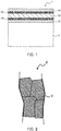
- Fig.1 shows the schematic diagram of the thin film capacitor (the capacitance element) according to the present embodiment.
- a lower electrode 12 and a dielectric thin film 13 are formed in this order on a substrate 11, and an upper electrode 14 is on the dielectric thin film 13.
- the material of the substrate 11 is not particularly limited, but Si single crystal substrate is used as the substrate 11 because of the cost and because it is easy to obtain. In case flexibility is important, Ni foil can be used as the substrate.
- the material of the lower electrode 12 and the upper electrode 14 are not particularly limited as long as these function as the electrode.
- Pt, Ag, and Ni or so may be mentioned.
- the thickness of the lower electrode 12 is preferably 0.01 to 10 ⁇ m.
- the thickness of the upper electrode 14 is preferably 0.01 to 10 ⁇ m.
- A is one or more elements selected from the group consisting of Sr, Ba, Ca, La, Ce, Pr, Nd and Na.
- A is one or more elements selected from the group consisting of Sr, Ba, La, and Nd. More preferably, “A” is Sr.
- B is one or more elements selected from the group consisting of Ta, Nb, Ti, and W.
- B is one or more elements selected from the group consisting of Ta and Nb. More preferably, “B” is Ta.
- a ⁇ 1 is satisfied.
- a/b > 1 is satisfied, and more preferably a/b ⁇ 1.05 is satisfied.
- preferably 1 > n > 0 is satisfied, more preferably 1 > n ⁇ 0.3, and more preferably 1 > n ⁇ 0.5 is satisfied.
- the crystalline particles X constituting the dielectric thin film 13 are polycrystalline which is not aligned to a specific crystal plane orientation.
- the crystalline particles X include plurality of longitudinal crystallite Y as shown in Fig.2 .
- the crystallite Y is a minimum unit of the crystalline constituted by same crystal plane in the crystalline particle X.
- a connection part between the crystallites Y has discontinuous crystal lattice, but this does not mean that a secondary phase or grain boundary exist at the connection part; and in fact it is continuous in terms of a composition and a crystallinity, further an aggregation of series of crystallites is the crystalline particles X.
- the crystal planes of plurality of the crystallites Y are aligned towards the same direction in one crystalline particle. A boundary which corresponds to a grain boundary exists at the connection part between the crystalline particles X and this can be observed by Transmission Electron Microscope (TEM).
- TEM Transmission Electron Microscope
- the size of the crystallite Y included in the crystalline particles X is 100 nm or less. Since the size of the crystallite Y is 100 nm or less, the dielectric property can be improved. The size of the crystallite Y is measured based on TEM image as shown in Fig.4 .
- the crystalline particles constituting the dielectric thin film are polycrystalline which are not aligned to a specific crystal plane orientation, and when the size of the crystallite included in the crystalline particles is 100 nm or less, the decrease rate of the dielectric constant with respect to the frequency can be suppressed to a small level, and at the same time the dielectric constant can be improved.
- the size of the crystallite calculated based on the result of X-ray diffraction measurement by Out-of-Plane method to the dielectric thin film 13 is preferably 1.5 times or more, more preferably 1.8 times or more, and further preferably 2.5 times or more of the size of the crystallite calculated based on the result of X-ray diffraction measurement by In-Plane method.
- the dielectric property can be improved by having the ratio between the size of the crystallite by Out-of-Plane method and the size of the crystallite by In-Plane method within the above mentioned range.
- incident X-ray R is irradiated within the angle range of 5 to 90° from the surface of the dielectric thin film as shown in Fig.3A , and the size of the crystallite is evaluated from the diffraction X-ray R' thereof. Thereby, the size of the crystallite in the thickness direction (the vertical direction) of the dielectric thin film can be measured.
- the incident X-ray R is irradiated from the side face of the dielectric thin film by fixing an incident angle to a small angle near a total reflection critical angle (0.2 to 0.5°), then the size of the crystallite is evaluated from the diffraction X-ray R'. Thereby, the size in the bilateral direction of the crystallite can be measured.
- the thickness of the dielectric thin film 13 is not particularly limited, but preferably it is 10 nm to 2 ⁇ m, and more preferably 10 nm to 1 ⁇ m.
- the dielectric constant ⁇ of the dielectric thin film 13 is not particularly limited, but preferably it is 1800 or more, more preferably 2500 or more, and further preferably 2700 or more. By having the dielectric constant ⁇ within the above mentioned range, the dielectric thin film having excellent dielectric property can be obtained.
- the dielectric constant ⁇ can be measured under the condition of the voltage of 1 Vrms/ ⁇ m, and the frequency of 20 Hz to 10 kHz.
- the dielectric constant decrease rate ⁇ of the dielectric thin film 13 is preferably less than ⁇ 20%, and more preferably within ⁇ 10%. By having the dielectric constant decrease rate ⁇ within the above mentioned range, the dielectric thin film having excellent dielectric property can be obtained.
- the dielectric constant decrease rate ⁇ can be calculated by dividing the difference between the dielectric constant measured at the frequency of 20 Hz and 10 kHz with the dielectric constant measured at the frequency of 20 Hz.
- the dielectric thin film 13 having the main composition including the oxynitride expressed by the compositional formula of A a B b O o N n wherein "A" atom is Sr, "B" atom is Ta will be used as an example to explain, but same applies even if other atoms are used.
- the film forming method for forming the thin film as the dielectric thin film 13 at the end is not particularly limited.
- a vacuum deposition method, a spattering method, PLD method (Pulse Laser Deposition method), MO-CVD method (Metal Organic Chemical Vapor Deposition method), MOD method (Metal Organic Decomposition method), a sol-gel method, and CSD method (Chemical Solution Deposition method) or so may be mentioned.
- trace amounts of impurities and sub components may be included in the material when forming the film; however it is not a problem as long as it is an amount which does not significantly compromise the property of the thin film.
- the dielectric thin film 13 according to the present embodiment may include trace amounts of impurities and sub components as long as these do not significantly compromise the property.
- the thin film obtained at the end is likely to be a polycrystalline film. It may be made by CVD method, but because many elements are included, PLD method and the spattering method or so have higher composition control property. In the present embodiment, the film forming method using PLD method will be described.
- Si single crystal substrate as the substrate 11 is prepared.
- SiO 2 , TiO x , and Pt are formed in this order on Si single crystal substrate, and the lower electrode 12 made of Pt is formed.
- the method of forming the lower electrode 12 is not particularly limited. For example, the spattering method and CVD method or so may be mentioned.
- the metal oxide thin film is formed on the lower electrode 12 by PLD method. Also, in order to expose part of the lower electrode 12, an area without the thin film is formed using a metal mask.
- a target including the constituting elements of the dielectric thin film as the object is placed in the film forming chamber.
- a pulse laser is irradiated on the surface of the target. Due to the strong energy of pulse laser, the surface of the target is instantly evaporated. Then, the evaporated substance is deposited on the substrate which is placed by facing towards the target, thereby the metal oxide thin film is formed.
- a precursor having the compositional formula A 2 B 2 O 7 can be used.
- This precursor is preferably a perovskite layer form compound wherein a perovskite unit called perovskite slab and an oxygen excess layer are stacked in an alternating manner.
- the type of target is not particularly limited, and a pellet formed by compressing the oxynitride powder can be used. Note that, N content included must be strictly regulated, thus the pellet of A 2 B 2 O 7 is used so that better controlling property can be attained. Also, for the target, preferably each element is distributed evenly, but the distribution may be uneven as long as the quality of the obtained dielectric thin film is not affected. Further, the target does not necessarily have to be one, and plurality of targets including part of the constituting elements of the dielectric thin film can be prepared and used for forming the film.
- the shape of the target is not particularly limited as well, and the shape may be which is appropriate for the film forming device being used.
- a and "b" of the dielectric thin film obtained at the end can be regulated. For example, by making a/b of the target large, a/b in the formed film can be enlarged as well.
- the composition of the dielectric thin film obtained at the end is Sr a Ta b O o N n
- a sintered body including Sr 2 Ta 2 O 7 is prepared as the target.
- the film forming condition for example, a partial pressure of oxygen, a partial pressure of nitrogen, the size of the film forming chamber, and the position of the gas introducing tube or so
- "a" and "b" of the dielectric thin film obtained at the end can be regulated.
- the film forming condition is also important.
- the metal element evaporated from the target due to the pulse laser is influenced by the elements constituting the atmosphere in the film forming chamber, and will reach to the film forming face of the substrate.
- the characteristic of PLD method is that it allows broad range of the atmospheric pressure from an extra high vacuum to near atmospheric pressure.
- the film with high crystallinity tends to be easily obtained when the vacuum condition is higher.
- the film with small defect of oxygen or so tends to be easily obtained when the atmospheric pressure of oxygen or so is higher.
- the range of pressure that the plasma can maintain is limited, thus appropriate pressure may be determined based on the crystallinity and defects or so within the range thereof.
- a total pressure is preferably 1 x 10 -2 Pa or more, and more preferably the total pressure is 2 x 10 -2 Pa or more.
- the preferable condition is the condition of which a degree of vacuum is relatively not high. This is a condition suitable for forming the film having small crystallite, and in this case the crystallinity is evaluated low.
- argon is preferably used together as the atmosphere while forming the film.
- the film forming rate is preferably 30 nm/min or less, and more preferably 10 nm/min or less.
- the substrate 11 when forming the film, is preferably heated by an infrared laser in order to crystalize the metal oxide thin film.
- a heating temperature of the substrate 11 differs depending on the constituting element and the composition or so of the metal oxide thin film and the substrate 11, but for example preferably it is 550 to 850°C, and more preferably 600 to 800°C.
- the dielectric thin film 13 made of perovskite type oxynitride can be obtained.
- the nitriding treatment may be done by introducing nitrogen radical after the metal oxide film is formed, but the nitrogen content in the thin film can be increased by introducing nitrogen radical while forming the film.
- the dielectric thin film 13 on the substrate needs to be carried out with Rapid Thermal Anneal (RTA) treatment after the film is formed.
- RTA Rapid Thermal Anneal
- the atmosphere during the annealing must have higher oxygen partial pressure and nitrogen partial pressure than the film forming atmosphere.
- the thin film capacitor 1 can be produced.
- the material of the upper electrode 14 is not particularly limited, and Ag, Au, and Cu or so can be used.
- the method of forming the upper electrode 14 is not particularly limited as well. For example, it can be formed by evaporation and the spattering method or so.
- an intermediate layer 15 may be present between the dielectric thin film 13 and the lower electrode 12, and between the dielectric thin film 13 and the upper electrode 14.
- the intermediate layer 15 may be constituted by an insulation material, and it may be constituted by a conductive material.
- the insulation material compounds such as oxides or nitrides including at least one selected from the group consisting of aluminum, silicon, strontium, and tantalum or so can be used.
- the conductive material Cu, Al, Ni, Au, and Ni-Cr or so can be used.
- the method of forming the intermediate layer 15 the same method as the method of forming the above mentioned dielectric thin film 13 or the method of forming the lower electrode 12 and the upper electrode 14 can be used.
- the intermediate layer 15 can function as the layer such as an insulation layer, a stress relieving layer, or a layer to smooth out a roughness of the electrode face or so.
- the intermediate layer 15 may be present at both between the dielectric thin film 13 and the lower electrode 12, and between the dielectric thin film 13 and the upper electrode 14, or it may be present at either one. If a plurality of intermediate layers is present, each intermediate layer may have different function.
- the thickness of the intermediate layer 15 is preferably 20% or less of the thickness of the dielectric thin layer 13, and more preferably 10% or less.
- the dielectric thin film according to the present embodiment can be used for example as a voltage tunable capacitor, and a dielectric layer of a high density capacitor device such as a decoupling thin film capacitor or so.
- the capacitance element according to the present embodiment is an element using an excellent dielectric property of the dielectric thin film according to the present embodiment, and a capacitor, a thermistor, a filter, a diplexer, a resonator, an emitter, an antenna, a piezoelectric element, a transistor, a ferroelectric memory or so are included.
- the dielectric thin film according to the present embodiment is suitably used to the capacitance element which requires particularly high dielectric characteristic.
- the method of producing the capacitor as an example of the capacitance element may be mentioned.
- the highly tunable device structure is not particularly limited, but for example that integrated with other thin film device such as SAW duplexer, a switch by RF-MEMS, MEMS air gap varactor of piezoelectric driving type, a fixed (low tunable) high density thin film capacitor, TFBAR circuit, a resistor, an inductor, and TFT having oxides as a base or so may be mentioned.
- SrCO 3 powder and Ta 2 O 5 powder were prepared as the material of a sintered body of Sr 2 Ta 2 O 7 used as the target for forming the film.
- SrCO 3 powder and Ta 2 O 5 powder were weighed so that a mol ratio of Sr/Ta was 1.
- the obtained post-calcination slurry was dried at 80°C for 12 hours using the thermostat drier, and a post-calcination mixture was obtained.
- the post-calcination mixture was added and mixed with polyvinyl alcohol as the binder, thereby a granule was obtained.
- the added amount of polyvinyl alcohol solution was 0.6 wt% with respect to 100 wt% of the ground material.
- the granule was molded into a cylindrical columnar shape having a diameter of about 23 mm, and a height of about 9 mm; thereby the molded article was obtained.
- the molding method was CIP molding.
- the molded article was fired under air atmosphere at 1400°C for 2 hours using the electric furnace; thereby a sintered article was obtained. Further, a top face and a bottom face of the sintered article was mirror polished, and the target for forming the film having a height of 5 mm was obtained. Note that, a relative density of the target for forming the film was 96 to 98%.
- the obtained target for forming the film as mentioned in above was placed to the film forming device, then Si substrate was placed by facing towards the target for forming the film.
- Si substrate those having Pt film as the lower electrode on the surface was used.
- the film was formed by PLD method so that the thickness was 1000 nm.
- nitrogen radical was introduced into the film forming chamber, and the dielectric oxide film was formed.
- the nitrogen partial pressure during the film forming was 1 x 10 -3 Pa.
- the film forming temperature was 700°C.
- the introduction of nitrogen radical was stopped, and at the same time nitrogen and oxygen were introduced, then the annealing was carried out for 30 minutes at 700°C. Then, it was cooled to 200°C, and the atmosphere was vacuumed, thereby the dielectric thin film sample was obtained.
- the obtained dielectric thin film sample was evaluated as discussed in below.
- the obtained sample was subjected to XRD measurement, thereby confirmed whether it was an alignment film aligned to specific plane and also confirmed whether it had polycrystallinity from XRD pattern. If polycrystallinity was confirmed and was not the alignment film aligned to specific plane, then it was evaluated as "good”; and if polycrystallinitiy was not confirmed and was the alignment film, then it was evaluated "poor”. Also, the composition of oxynitride included in the obtained thin film sample was quantified by photoelectron spectroscopy using PHI Quantera IITM made by ULVAC-PHI, Inc. While carrying out Ar etching, the composition in the depth direction of the thin film was quantified.
- TEM image was obtained using Transmission Electron Microscope (TEM).
- TEM Transmission Electron Microscope
- Fig.4 Based on TEM image shown in Fig.4 , the size of crystallite was measured. Also, the presence of the particle having the columnar shape was verified using TEM. The results are shown in Table 1.
- the size of crystallite was measured by Out-of-Plane method and In-Plane method.
- the dielectric constant ( ⁇ ) was evaluated under the voltage of 1 Vrms/ ⁇ m and the frequency of 20 Hz to 10 kHz, and then the decrease rate was calculated.
- the upper electrode for evaluating the dielectric constant was formed by depositing Ag on the electrode having the size of 100 ⁇ m of diameter. The results are shown in Table 1.
- the dielectric constant decrease rate ⁇ was measured.
- the dielectric constant decrease rate ⁇ was calculated by dividing the difference between the dielectric constant measured at the frequency of 20 Hz and 10 kHz with the dielectric constant measured at the frequency of 20 Hz.
- the atmosphere during the film forming was adjusted so that the size of the crystallite by XRD was regulated as shown in Table 1, other than that the dielectric thin film sample was obtained as same as the example 1.
- the evaluation was carried out as same as the example 1.
- the dielectric thin film sample was obtained as same as the example 3 except for the following. That is, in the example 5, as the material of the sintered body of (La 0.1 Sr 0.9 ) 2 (Ta 0.9 Ti 0 . 1 ) 2 O 7 used as the target for forming the film, La 2 O 3 powder, SrCO 3 powder, Ta 2 O 5 powder, and TiO 2 powder were prepared. La 2 O 3 powder, SrCO 3 powder, Ta 2 O 5 powder, and TiO 2 powder were weighed so that the mol ratio of (La 0.1 Sr 0.9 )/(Ta 0.9 Ti 0.1 ) was 1.
- the dielectric thin film sample was obtained as same as the example 3 except for the following. That is, in the example 6, as the material of the sintered body of (Ba 0.2 Sr 0.8 ) 2 Ta 2 O 7 used as the target for forming the film, BaCO 3 powder, SrCO 3 powder, and Ta 2 O 5 powder were prepared. BaCO 3 powder, SrCO 3 powder, and Ta 2 O 5 powder were weighed so that the mol ratio of (Ba 0.2 Sr 0.8 )/(Ta) was 1. Sr 2 Ta 2 O 7 composition exists as the sintered body having the perovskite slab structure; on the contrary Ba 2 Ta 2 O 7 does not exist.
- the sintered body of (Ba 0.2 Sr 0.8 ) 2 Ta 2 O 7 composition can be obtained.
- the obtained sintered body has the same X-ray diffraction pattern as Sr 2 Ta 2 O 7 , and the peak positon thereof shifted to the lower angle side.
- the comparative example 1 was calculated from the non-patent document 1.
- the non-patent document 1 forms SrTaO 2 N thin film crystal sample by carrying out the epitaxial growth using a nitrogen plasma assisted pulse laser deposition method. Specifically, using niobium added strontium titanate (Nb:SrTiO 3 ) single crystal having smaller lattice constant than SrTaO 2 N as the substrate for the crystal growth, and strontium tantalate vaporized by irradiating the ultraviolet laser and nitrogen activated by plasma were reacted. The same evaluation as the example 1 was carried out. The results are shown in Table 1.
- the dielectric thin film sample formed of the crystalline particles which are polycrystalline not aligned to a specific crystal plane orientation was obtained, and exhibited excellent dielectric property.
- the dielectric thin film sample of the comparative example 1 had the size of the crystallite included in the crystalline particles larger than 100 nm, and the decrease rate of the dielectric constant with respect to the frequency was deteriorated.
Landscapes
- Engineering & Computer Science (AREA)
- Chemical & Material Sciences (AREA)
- Power Engineering (AREA)
- Ceramic Engineering (AREA)
- Manufacturing & Machinery (AREA)
- Microelectronics & Electronic Packaging (AREA)
- Inorganic Chemistry (AREA)
- Organic Chemistry (AREA)
- Materials Engineering (AREA)
- Structural Engineering (AREA)
- Fixed Capacitors And Capacitor Manufacturing Machines (AREA)
- Inorganic Insulating Materials (AREA)
- Semiconductor Memories (AREA)
Abstract
The object of the present invention is to provide a dielectric thin film and a capacitance element having excellent dielectric property.
A dielectric thin film comprising a main component comprised of an oxynitride expressed by a compositional formula of AaBbOoNn (a + b + o + n =5), wherein said "A" is one or more selected from the group consisting of Sr, Ba, Ca, La, Ce, Pr, Nd, and Na, said "B" is one or more selected from the group consisting of Ta, Nb, Ti, and W, and crystalline particles constituting said dielectric thin film are polycrystalline which are not aligned to a particular crystal plane orientation, and a size of a crystallite of the crystalline particles included in the dielectric thin film is 100 nm or less.
Description
- The present invention relates to a dielectric thin film having a main component comprised of an oxynitride, and a capacitance including the dielectric thin film.
- As digital devices have been down sized and have attained higher performances in recent years, the capacitance element using a high performance dielectric thin film is demanded.
- Conventionally, a thin film using metal oxide material has been widely used as the dielectric thin film. However, the improvement of the property of the dielectric thin film made by the metal oxide material is reaching its limits, and new material having higher property is demanded. As one of the proposed new materials, a metal oxynitride material may be mentioned of which part of oxygen atoms in oxygen-octahedron structure of perovskite type crystal structure are substituted with nitrogen atoms. However, the dielectric thin film having the metal oxynitride material is difficult to obtain.
- For example, a
patent document 1 and a patent document 2 disclose a method of producing a powder of perovskite type oxynitride ABO2N. However, thepatent document 1 and the patent document 2 do not disclose of obtaining a thin film using the perovskite type oxynitride ABO2N. - Also, the
non-patent document 1 and the non-patent document 2 disclose that the thin film made of the perovskite type oxynitride ABO2N was produced. However, the thin film obtained in anon-patent document 1 and a non-patent document 2 is an epitaxial film. - The epitaxial film has a disadvantage that it takes extremely long time to produce. The
non-patent document 1 discloses that the production of the epitaxial film having a thickness of 20 nm or less took 530 hours or less, which is a long time. - [Patent document 1]
JP Patent Application Laid Open No.S61-122108 - [Patent document 2]
JP Patent Application Laid Open No.2013-001625 - [Non-patent document 1] Scientific Reports 4. DOI: 10.1038/srep04987
- [Non-patent document 2] KAST Year 2013 Research outline p.32-33
- The present invention is attained in view of such circumstances, and the object is to provide the dielectric thin film having a main component made of oxynitride having high production efficiency and excellent dielectric property, and to provide the capacitance element including the dielectric thin film.
- The dielectric thin film according to the present invention is a dielectric thin film comprising a main component comprised of an oxynitride expressed by a compositional formula of AaBbOoNn (a + b + o + n =5), wherein
- "A" is one or more selected from the group consisting of Sr, Ba, Ca, La, Ce, Pr, Nd, and Na,
- "B" is one or more selected from the group consisting of Ta, Nb, Ti, and W, and
- crystalline particles constituting said dielectric thin film are polycrystalline which are not aligned to a particular crystal plane orientation, and a size of a crystallite of the crystalline particles included in the dielectric thin film is 100 nm or less.
- The dielectric thin film according to the present invention has the above mentioned characteristics, and thereby the dielectric property can be enhanced.
- Preferably, the size of the crystallite calculated based on a result of X-ray diffraction measurement using Out-of-Plane method to the dielectric thin film is 1.5 times or more of the size of the crystallite calculated based on X-ray diffraction measurement using In-Plane method.
- Preferably, "A" is Sr, "B" is Ta and/or Nb, and "n" is larger than 0 and smaller than 1.
- The capacitance element according to the present invention comprises the dielectric thin film.
-
- [
Fig.1] Fig.1 is a schematic diagram of a thin film capacitor according to one embodiment of the present invention. - [
Fig.2] Fig.2 is a schematic diagram showing the shape of crystallite included in the crystalline particles in the dielectric thin film according to one embodiment of the present invention. - [
Fig.3A] Fig.3A is a schematic diagram showing X-ray diffraction measurement by Out-of-Plane method. - [
Fig.3B] Fig.3B is a schematic diagram showing X-ray diffraction measurement by In-Plane method. - [
Fig.4] Fig.4 is TEM image of a dielectric thin film sample of the example 1. The broken line shows the shape of the crystallite. - Hereinafter, the present invention will be explained by referring to embodiments.
-
Fig.1 shows the schematic diagram of the thin film capacitor (the capacitance element) according to the present embodiment. In thethin film capacitor 1 shown inFig.1 , alower electrode 12 and a dielectricthin film 13 are formed in this order on asubstrate 11, and anupper electrode 14 is on the dielectricthin film 13. - The material of the
substrate 11 is not particularly limited, but Si single crystal substrate is used as thesubstrate 11 because of the cost and because it is easy to obtain. In case flexibility is important, Ni foil can be used as the substrate. - The material of the
lower electrode 12 and theupper electrode 14 are not particularly limited as long as these function as the electrode. For example, Pt, Ag, and Ni or so may be mentioned. The thickness of thelower electrode 12 is preferably 0.01 to 10 µm. The thickness of theupper electrode 14 is preferably 0.01 to 10 µm. - The dielectric
thin film 13 has the main component made of oxynitride expressed by the compositional formula of AaBbOoNn (a + b + o + n = 5). - "A" is one or more elements selected from the group consisting of Sr, Ba, Ca, La, Ce, Pr, Nd and Na. Preferably, "A" is one or more elements selected from the group consisting of Sr, Ba, La, and Nd. More preferably, "A" is Sr. By using the above mentioned elements as "A"; a high capacitance can be obtained. "B" is one or more elements selected from the group consisting of Ta, Nb, Ti, and W. Preferably, "B" is one or more elements selected from the group consisting of Ta and Nb. More preferably, "B" is Ta. By using the above mentioned elements as "B", the dielectric
thin film 13 with little secondary phase can be obtained. - Also, in the compositional formula AaBbOoNn, preferably a < 1 is satisfied. Also, preferably, a/b > 1 is satisfied, and more preferably a/b ≥ 1.05 is satisfied. Also, preferably 1 > n > 0 is satisfied, more preferably 1 > n ≥ 0.3, and more preferably 1 > n ≥ 0.5 is satisfied. By having "a", "b", and "n" within the above mentioned range, a good dielectric property can be obtained.
- The crystalline particles X constituting the dielectric
thin film 13 are polycrystalline which is not aligned to a specific crystal plane orientation. - The crystalline particles X include plurality of longitudinal crystallite Y as shown in
Fig.2 . The crystallite Y is a minimum unit of the crystalline constituted by same crystal plane in the crystalline particle X. Thus, a connection part between the crystallites Y has discontinuous crystal lattice, but this does not mean that a secondary phase or grain boundary exist at the connection part; and in fact it is continuous in terms of a composition and a crystallinity, further an aggregation of series of crystallites is the crystalline particles X. The crystal planes of plurality of the crystallites Y are aligned towards the same direction in one crystalline particle. A boundary which corresponds to a grain boundary exists at the connection part between the crystalline particles X and this can be observed by Transmission Electron Microscope (TEM). - In the present embodiment, the size of the crystallite Y included in the crystalline particles X is 100 nm or less. Since the size of the crystallite Y is 100 nm or less, the dielectric property can be improved. The size of the crystallite Y is measured based on TEM image as shown in
Fig.4 . - In general, it is known that by decreasing the size of the crystallite included in the crystalline particles constituting the dielectric thin film, a decrease rate of the dielectric constant with respect to the frequency can be suppressed to a small level. On the other hand, when the size of the crystallite is decreased, it is known that the obtained dielectric constant is also decreased. Particularly, it is known that for barium titanate used as high capacity dielectrics, by decreasing the size of the crystallite, a high tetragonality (c/a ratio) at close-packed hexagonal lattice becomes difficult to obtain; and when the size of crystallite is 100 nm or less, it is known that the dielectric constant decreases drastically. If high dielectric constant can be obtained even when the size of the crystallite is 100 nm or less, then ideal dielectrics having small decrease of the permittivity with respect to the frequency can be attained, however such dielectrics have not been reported yet. In the present embodiment, the crystalline particles constituting the dielectric thin film are polycrystalline which are not aligned to a specific crystal plane orientation, and when the size of the crystallite included in the crystalline particles is 100 nm or less, the decrease rate of the dielectric constant with respect to the frequency can be suppressed to a small level, and at the same time the dielectric constant can be improved.
- Also, the size of the crystallite calculated based on the result of X-ray diffraction measurement by Out-of-Plane method to the dielectric
thin film 13 is preferably 1.5 times or more, more preferably 1.8 times or more, and further preferably 2.5 times or more of the size of the crystallite calculated based on the result of X-ray diffraction measurement by In-Plane method. The dielectric property can be improved by having the ratio between the size of the crystallite by Out-of-Plane method and the size of the crystallite by In-Plane method within the above mentioned range. - Note that, for Out-of-Plane method, incident X-ray R is irradiated within the angle range of 5 to 90° from the surface of the dielectric thin film as shown in
Fig.3A , and the size of the crystallite is evaluated from the diffraction X-ray R' thereof. Thereby, the size of the crystallite in the thickness direction (the vertical direction) of the dielectric thin film can be measured. - Also, as shown in
Fig.3B , for In-Plane method, the incident X-ray R is irradiated from the side face of the dielectric thin film by fixing an incident angle to a small angle near a total reflection critical angle (0.2 to 0.5°), then the size of the crystallite is evaluated from the diffraction X-ray R'. Thereby, the size in the bilateral direction of the crystallite can be measured. - The thickness of the dielectric
thin film 13 is not particularly limited, but preferably it is 10 nm to 2 µm, and more preferably 10 nm to 1 µm. - The dielectric constant ε of the dielectric
thin film 13 is not particularly limited, but preferably it is 1800 or more, more preferably 2500 or more, and further preferably 2700 or more. By having the dielectric constant ε within the above mentioned range, the dielectric thin film having excellent dielectric property can be obtained. - Note that, the dielectric constant ε can be measured under the condition of the voltage of 1 Vrms/µm, and the frequency of 20 Hz to 10 kHz.
- The dielectric constant decrease rate Δε of the dielectric
thin film 13 is preferably less than ± 20%, and more preferably within ± 10%. By having the dielectric constant decrease rate Δε within the above mentioned range, the dielectric thin film having excellent dielectric property can be obtained. - Note that, the dielectric constant decrease rate Δε can be calculated by dividing the difference between the dielectric constant measured at the frequency of 20 Hz and 10 kHz with the dielectric constant measured at the frequency of 20 Hz.
- Next, the production method of the
thin film capacitor 1 will be explained. Hereinafter, the dielectricthin film 13 having the main composition including the oxynitride expressed by the compositional formula of AaBbOoNn wherein "A" atom is Sr, "B" atom is Ta will be used as an example to explain, but same applies even if other atoms are used. - The film forming method for forming the thin film as the dielectric
thin film 13 at the end is not particularly limited. For example, a vacuum deposition method, a spattering method, PLD method (Pulse Laser Deposition method), MO-CVD method (Metal Organic Chemical Vapor Deposition method), MOD method (Metal Organic Decomposition method), a sol-gel method, and CSD method (Chemical Solution Deposition method) or so may be mentioned. Also, trace amounts of impurities and sub components may be included in the material when forming the film; however it is not a problem as long as it is an amount which does not significantly compromise the property of the thin film. Also, the dielectricthin film 13 according to the present embodiment may include trace amounts of impurities and sub components as long as these do not significantly compromise the property. - Among the method of forming the film, when the film is formed by PLD method, the spattering method, and CSD method or so, the thin film obtained at the end is likely to be a polycrystalline film. It may be made by CVD method, but because many elements are included, PLD method and the spattering method or so have higher composition control property. In the present embodiment, the film forming method using PLD method will be described.
- First, Si single crystal substrate as the
substrate 11 is prepared. Next, SiO2, TiOx, and Pt are formed in this order on Si single crystal substrate, and thelower electrode 12 made of Pt is formed. The method of forming thelower electrode 12 is not particularly limited. For example, the spattering method and CVD method or so may be mentioned. - Next, the metal oxide thin film is formed on the
lower electrode 12 by PLD method. Also, in order to expose part of thelower electrode 12, an area without the thin film is formed using a metal mask. - In PLD method, first a target including the constituting elements of the dielectric thin film as the object is placed in the film forming chamber. Next, a pulse laser is irradiated on the surface of the target. Due to the strong energy of pulse laser, the surface of the target is instantly evaporated. Then, the evaporated substance is deposited on the substrate which is placed by facing towards the target, thereby the metal oxide thin film is formed.
- As the target, for example, a precursor having the compositional formula A2B2O7 can be used. This precursor is preferably a perovskite layer form compound wherein a perovskite unit called perovskite slab and an oxygen excess layer are stacked in an alternating manner.
- The type of target is not particularly limited, and a pellet formed by compressing the oxynitride powder can be used. Note that, N content included must be strictly regulated, thus the pellet of A2B2O7 is used so that better controlling property can be attained. Also, for the target, preferably each element is distributed evenly, but the distribution may be uneven as long as the quality of the obtained dielectric thin film is not affected. Further, the target does not necessarily have to be one, and plurality of targets including part of the constituting elements of the dielectric thin film can be prepared and used for forming the film. The shape of the target is not particularly limited as well, and the shape may be which is appropriate for the film forming device being used. By regulating the film forming condition (a partial pressure of oxygen, a partial pressure of nitrogen, the size of the film forming chamber, and the position of the gas introducing tube or so), "a" and "b" of the dielectric thin film obtained at the end can be regulated. For example, by making a/b of the target large, a/b in the formed film can be enlarged as well.
- For example, in case the composition of the dielectric thin film obtained at the end is SraTabOoNn, then a sintered body including Sr2Ta2O7 is prepared as the target. Further, by regulating the film forming condition (for example, a partial pressure of oxygen, a partial pressure of nitrogen, the size of the film forming chamber, and the position of the gas introducing tube or so), "a" and "b" of the dielectric thin film obtained at the end can be regulated.
- The film forming condition is also important. The metal element evaporated from the target due to the pulse laser is influenced by the elements constituting the atmosphere in the film forming chamber, and will reach to the film forming face of the substrate. The characteristic of PLD method is that it allows broad range of the atmospheric pressure from an extra high vacuum to near atmospheric pressure. However, the film with high crystallinity tends to be easily obtained when the vacuum condition is higher. On the other hand, the film with small defect of oxygen or so tends to be easily obtained when the atmospheric pressure of oxygen or so is higher. When plasma is used together, the range of pressure that the plasma can maintain is limited, thus appropriate pressure may be determined based on the crystallinity and defects or so within the range thereof. Particularly, when forming the film by PLD method, a total pressure is preferably 1 x 10⁻² Pa or more, and more preferably the total pressure is 2 x 10⁻² Pa or more. The preferable condition is the condition of which a degree of vacuum is relatively not high. This is a condition suitable for forming the film having small crystallite, and in this case the crystallinity is evaluated low. Note that, for the spattering method, argon is preferably used together as the atmosphere while forming the film. The film forming rate is preferably 30 nm/min or less, and more preferably 10 nm/min or less.
- Also, for PLD method, when forming the film, the
substrate 11 is preferably heated by an infrared laser in order to crystalize the metal oxide thin film. A heating temperature of thesubstrate 11 differs depending on the constituting element and the composition or so of the metal oxide thin film and thesubstrate 11, but for example preferably it is 550 to 850°C, and more preferably 600 to 800°C. By making the temperature of the substrate within the above mentioned range while forming the film, the dielectric property improves because pore is scarcely formed. Also, since the temperature of thesubstrate 11 has an appropriate temperature, the metal oxynitride thin film tends to easily crystalize, and the cracks generated while cooling can be prevented. - When forming the film, by carrying out a nitriding treatment by introducing nitrogen radical, the dielectric
thin film 13 made of perovskite type oxynitride can be obtained. The nitriding treatment may be done by introducing nitrogen radical after the metal oxide film is formed, but the nitrogen content in the thin film can be increased by introducing nitrogen radical while forming the film. - The dielectric
thin film 13 on the substrate needs to be carried out with Rapid Thermal Anneal (RTA) treatment after the film is formed. In order to improve the frequency characteristic, the atmosphere during the annealing must have higher oxygen partial pressure and nitrogen partial pressure than the film forming atmosphere. - Lastly, by forming the
upper electrode 14 on the dielectricthin film 13, thethin film capacitor 1 can be produced. Note that, the material of theupper electrode 14 is not particularly limited, and Ag, Au, and Cu or so can be used. Also, the method of forming theupper electrode 14 is not particularly limited as well. For example, it can be formed by evaporation and the spattering method or so. - Note that, an
intermediate layer 15 may be present between the dielectricthin film 13 and thelower electrode 12, and between the dielectricthin film 13 and theupper electrode 14. Theintermediate layer 15 may be constituted by an insulation material, and it may be constituted by a conductive material. As the insulation material, compounds such as oxides or nitrides including at least one selected from the group consisting of aluminum, silicon, strontium, and tantalum or so can be used. As the conductive material, Cu, Al, Ni, Au, and Ni-Cr or so can be used. As the method of forming theintermediate layer 15, the same method as the method of forming the above mentioned dielectricthin film 13 or the method of forming thelower electrode 12 and theupper electrode 14 can be used. Further, theintermediate layer 15 can function as the layer such as an insulation layer, a stress relieving layer, or a layer to smooth out a roughness of the electrode face or so. - The
intermediate layer 15 may be present at both between the dielectricthin film 13 and thelower electrode 12, and between the dielectricthin film 13 and theupper electrode 14, or it may be present at either one. If a plurality of intermediate layers is present, each intermediate layer may have different function. - The thickness of the
intermediate layer 15 is preferably 20% or less of the thickness of the dielectricthin layer 13, and more preferably 10% or less. - The dielectric thin film according to the present embodiment can be used for example as a voltage tunable capacitor, and a dielectric layer of a high density capacitor device such as a decoupling thin film capacitor or so.
- The capacitance element according to the present embodiment is an element using an excellent dielectric property of the dielectric thin film according to the present embodiment, and a capacitor, a thermistor, a filter, a diplexer, a resonator, an emitter, an antenna, a piezoelectric element, a transistor, a ferroelectric memory or so are included. The dielectric thin film according to the present embodiment is suitably used to the capacitance element which requires particularly high dielectric characteristic.
- As the method of producing the capacitor as an example of the capacitance element according to the present embodiment, the method of forming a highly tunable device structure having an appropriate electrode on the substrate may be mentioned. The highly tunable device structure is not particularly limited, but for example that integrated with other thin film device such as SAW duplexer, a switch by RF-MEMS, MEMS air gap varactor of piezoelectric driving type, a fixed (low tunable) high density thin film capacitor, TFBAR circuit, a resistor, an inductor, and TFT having oxides as a base or so may be mentioned.
- Hereinabove, the embodiments of the present invention were explained, but the present invention is not to be limited to these embodiments in any way, and the present invention can be carried out in various different embodiments within the scope of the present invention.
- Hereinafter, the present invention will be described based on further detailed examples, but the present invention is not to be limited thereto.
- First, as the material of a sintered body of Sr2Ta2O7 used as the target for forming the film, SrCO3 powder and Ta2O5 powder were prepared. SrCO3 powder and Ta2O5 powder were weighed so that a mol ratio of Sr/Ta was 1.
- Next, SrCO3 powder and Ta2O5 powder were mixed for 16 hours by a wet ball mill using ethanol solvent, thereby a mixed slurry was obtained.
- Next, said mixed slurry was dried at 80°C for 12 hours using a thermostat drier, and the mixture was obtained.
- Next, said mixture was lightly ground in a mortar, and then placed in a ceramic crucible. Then, using an electric furnace, the heat treatment was carried out under air atmosphere at 1000°C for 2 hours; thereby the calcined material was obtained.
- Next, said calcined material was again mixed for 16 hours by a wet ball mill using ethanol solvent, and then a post-calcination slurry was obtained.
- The obtained post-calcination slurry was dried at 80°C for 12 hours using the thermostat drier, and a post-calcination mixture was obtained.
- The post-calcination mixture was added and mixed with polyvinyl alcohol as the binder, thereby a granule was obtained. The added amount of polyvinyl alcohol solution was 0.6 wt% with respect to 100 wt% of the ground material.
- The granule was molded into a cylindrical columnar shape having a diameter of about 23 mm, and a height of about 9 mm; thereby the molded article was obtained. The molding method was CIP molding.
- The molded article was fired under air atmosphere at 1400°C for 2 hours using the electric furnace; thereby a sintered article was obtained. Further, a top face and a bottom face of the sintered article was mirror polished, and the target for forming the film having a height of 5 mm was obtained. Note that, a relative density of the target for forming the film was 96 to 98%.
- The obtained target for forming the film as mentioned in above was placed to the film forming device, then Si substrate was placed by facing towards the target for forming the film. As Si substrate, those having Pt film as the lower electrode on the surface was used.
- In the example 1, the film was formed by PLD method so that the thickness was 1000 nm. Here, nitrogen radical was introduced into the film forming chamber, and the dielectric oxide film was formed. The nitrogen partial pressure during the film forming was 1 x 10⁻³ Pa. The film forming temperature was 700°C. After forming the film, the introduction of nitrogen radical was stopped, and at the same time nitrogen and oxygen were introduced, then the annealing was carried out for 30 minutes at 700°C. Then, it was cooled to 200°C, and the atmosphere was vacuumed, thereby the dielectric thin film sample was obtained. The obtained dielectric thin film sample was evaluated as discussed in below.
- The obtained sample was subjected to XRD measurement, thereby confirmed whether it was an alignment film aligned to specific plane and also confirmed whether it had polycrystallinity from XRD pattern. If polycrystallinity was confirmed and was not the alignment film aligned to specific plane, then it was evaluated as "good"; and if polycrystallinitiy was not confirmed and was the alignment film, then it was evaluated "poor". Also, the composition of oxynitride included in the obtained thin film sample was quantified by photoelectron spectroscopy using PHI Quantera II™ made by ULVAC-PHI, Inc. While carrying out Ar etching, the composition in the depth direction of the thin film was quantified.
- For the obtained sample, TEM image was obtained using Transmission Electron Microscope (TEM). The obtained TEM image is shown in
Fig.4 . Based on TEM image shown inFig.4 , the size of crystallite was measured. Also, the presence of the particle having the columnar shape was verified using TEM. The results are shown in Table 1. - For the obtained sample, the size of crystallite was measured by Out-of-Plane method and In-Plane method.
- The dielectric constant (ε) was evaluated under the voltage of 1 Vrms/µm and the frequency of 20 Hz to 10 kHz, and then the decrease rate was calculated. The upper electrode for evaluating the dielectric constant was formed by depositing Ag on the electrode having the size of 100 µm of diameter. The results are shown in Table 1.
- For the sample formed with the Ag electrode, the dielectric constant decrease rate Δε was measured. The dielectric constant decrease rate Δε was calculated by dividing the difference between the dielectric constant measured at the frequency of 20 Hz and 10 kHz with the dielectric constant measured at the frequency of 20 Hz.
- The atmosphere during the film forming was adjusted so that the size of the crystallite by XRD was regulated as shown in Table 1, other than that the dielectric thin film sample was obtained as same as the example 1. The evaluation was carried out as same as the example 1.
- The dielectric thin film sample was obtained as same as the example 3 except for the following. That is, in the example 5, as the material of the sintered body of (La0.1Sr0.9)2(Ta0.9Ti0.1)2O7 used as the target for forming the film, La2O3 powder, SrCO3 powder, Ta2O5 powder, and TiO2 powder were prepared. La2O3 powder, SrCO3 powder, Ta2O5 powder, and TiO2 powder were weighed so that the mol ratio of (La0.1Sr0.9)/(Ta0.9Ti0.1) was 1.
- The dielectric thin film sample was obtained as same as the example 3 except for the following. That is, in the example 6, as the material of the sintered body of (Ba0.2Sr0.8)2Ta2O7 used as the target for forming the film, BaCO3 powder, SrCO3 powder, and Ta2O5 powder were prepared. BaCO3 powder, SrCO3 powder, and Ta2O5 powder were weighed so that the mol ratio of (Ba0.2Sr0.8)/(Ta) was 1. Sr2Ta2O7 composition exists as the sintered body having the perovskite slab structure; on the contrary Ba2Ta2O7 does not exist. However, by weighing and blending BaCO3 powder, SrCO3 powder, and Ta2O5 powder so to satisfy the mol ratio of (Ba0.2Sr0.8)/(Ta) of 1, the sintered body of (Ba0.2Sr0.8)2Ta2O7 composition can be obtained. The obtained sintered body has the same X-ray diffraction pattern as Sr2Ta2O7, and the peak positon thereof shifted to the lower angle side.
- The comparative example 1 was calculated from the
non-patent document 1. Thenon-patent document 1 forms SrTaO2N thin film crystal sample by carrying out the epitaxial growth using a nitrogen plasma assisted pulse laser deposition method. Specifically, using niobium added strontium titanate (Nb:SrTiO3) single crystal having smaller lattice constant than SrTaO2N as the substrate for the crystal growth, and strontium tantalate vaporized by irradiating the ultraviolet laser and nitrogen activated by plasma were reacted. The same evaluation as the example 1 was carried out. The results are shown in Table 1. - In the examples 7 to 12, the dielectric thin film sample was obtained as same as the example 1, except that the film was formed by changing the nitrogen partial pressure in the atmosphere during the film forming. The same evaluation as the example 1 was carried out. The results are shown in Table 1.
[Table 1] Composition Particles of column form Size of crystallite XRD Dielectric property Polycrystallinity Out-of-Plane In-Plane Ratio Dielectric constant ε Dielectric constant decrease rate Δ ε Example 1 SrTaO2N Present <100nm Good 20.2 7.1 2.85 3000 -4% Example 2 SrTaO2N Present <100nm Good 16.8 10.9 1.5 2211 -9% Example 3 SrTaO2N Present <100nm Good 162 9.0 1.8 2533 -6% Example 4 SrTaO2N Present <100nm Good 17.3 10.2 1.7 1886 -9% Example 5 (La0.1Sr0.9)(Ta0.9Ti0.1)O2N Present <100nm Good 18.1 11.8 1.5 2710 -9% Example 6 (Ba0.2Sr0.8)TaO2N Present <100nm Good 15.4 8.7 1.8 1990 -7% Example 7 SrTaO2N Present <100nm Good 9.4 19.6 0.5 851 -48% Example 8 SrTaO2N Present <100nm Good 9.9 17.4 0.6 739 -50% Example 9 SrTaO2N Present <100nm Good 13.4 15.6 0.9 3020 -21% Example 10 SrTaO2N Present <100nm Good 10.8 23.6 0.5 1415 -48% Example 11 SrTaO2N Present <100nm Good 9.9 20.7 0.5 1671 -45% Example 12 SrTaO2N Present <100nm Good 10.3 20.3 0.5 1364 -48% Comparative example 1 SrTaO2N None 288nm Good - - - 2300 -20% - According to Table 1, for the examples 1 to 12, the dielectric thin film sample formed of the crystalline particles which are polycrystalline not aligned to a specific crystal plane orientation was obtained, and exhibited excellent dielectric property. On the other hand, the dielectric thin film sample of the comparative example 1 had the size of the crystallite included in the crystalline particles larger than 100 nm, and the decrease rate of the dielectric constant with respect to the frequency was deteriorated.
-
- 1 ...Thin film capacitor
- 11 ... Substrate
- 12...Lower electrode
- 14...Upper electrode
- 15...Intermediate layer
- X...Crystalline particle
- Y...Crystallite
- R...Incident X-ray
- R'...Diffraction X-ray
Claims (4)
- A dielectric thin film comprising a main component comprised of an oxynitride expressed by a compositional formula of AaBbOoNn (a + b + o + n =5), wherein"A" is one or more selected from the group consisting of Sr, Ba, Ca, La, Ce, Pr, Nd, and Na,"B" is one or more selected from the group consisting of Ta, Nb, Ti, and W, andcrystalline particles constituting said dielectric thin film are polycrystalline which are not aligned to a particular crystal plane orientation, and a size of a crystallite of the crystalline particles included in the dielectric thin film is 100 nm or less.
- The dielectric thin film according to claim 1, wherein the size of the crystallite calculated based on a result of X-ray diffraction measurement using Out-of-Plane method to the dielectric thin film is 1.5 times or more of the size of the crystallite calculated based on X-ray diffraction measurement using In-Plane method.
- The dielectric thin film according to claim 1, wherein "A" is Sr, "B" is Ta and/or Nb, and "n" is larger than 0 and smaller than 1.
- A capacitance element comprising the dielectric thin film according to claim 1.
Applications Claiming Priority (2)
| Application Number | Priority Date | Filing Date | Title |
|---|---|---|---|
| JP2017071119 | 2017-03-31 | ||
| JP2018013707A JP7000883B2 (en) | 2017-03-31 | 2018-01-30 | Oxynitride thin film and capacitive element |
Publications (1)
| Publication Number | Publication Date |
|---|---|
| EP3382727A1 true EP3382727A1 (en) | 2018-10-03 |
Family
ID=62165295
Family Applications (1)
| Application Number | Title | Priority Date | Filing Date |
|---|---|---|---|
| EP18165031.8A Pending EP3382727A1 (en) | 2017-03-31 | 2018-03-29 | Oxynitride thin film and capacitance element |
Country Status (4)
| Country | Link |
|---|---|
| US (1) | US10475586B2 (en) |
| EP (1) | EP3382727A1 (en) |
| KR (1) | KR102033058B1 (en) |
| CN (1) | CN108695064B (en) |
Families Citing this family (4)
| Publication number | Priority date | Publication date | Assignee | Title |
|---|---|---|---|---|
| WO2020102416A1 (en) * | 2018-11-13 | 2020-05-22 | Drexel University | Nanocrystalline high-k low-leakage thin films |
| CN113233901B (en) * | 2021-06-30 | 2022-05-31 | 中国人民解放军国防科技大学 | Compact high-purity strontium tantalum oxynitride ceramic and preparation method thereof |
| CN113264776B (en) * | 2021-06-30 | 2022-02-22 | 中国人民解放军国防科技大学 | Compact europium tantalum oxynitride ceramic and preparation method thereof |
| JP7748322B2 (en) * | 2022-03-30 | 2025-10-02 | Tdk株式会社 | Dielectric Elements |
Citations (4)
| Publication number | Priority date | Publication date | Assignee | Title |
|---|---|---|---|---|
| JPS61122108A (en) | 1984-11-13 | 1986-06-10 | サントル・ナシヨナル・ドウ・ラ・ルシエルシユ・サイエンテイフイツク(セー・エヌ・エル・エス) | Nitrogen or oxynitrogen compound having a perovskite structure, method for producing the same, and method for using the same for producing a dielectric material |
| EP1078998A2 (en) * | 1999-08-20 | 2001-02-28 | Matsushita Electric Industrial Co., Ltd. | Dielectric film with a perovskite structure and method of fabricating the same |
| JP2013001625A (en) | 2011-06-21 | 2013-01-07 | Showa Denko Kk | Dielectric composition and method for manufacturing the same |
| US20130154443A1 (en) * | 2011-12-19 | 2013-06-20 | Canon Kabushiki Kaisha | Piezoelectric material, piezoelectric element, liquid ejection head, ultrasonic motor, and dust removing device |
Family Cites Families (4)
| Publication number | Priority date | Publication date | Assignee | Title |
|---|---|---|---|---|
| JP4107792B2 (en) * | 2000-08-28 | 2008-06-25 | 独立行政法人科学技術振興機構 | Photocatalyst composed of metal oxynitride having visible light response |
| WO2003101615A1 (en) * | 2002-06-03 | 2003-12-11 | Asahi Kasei Kabushiki Kaisha | Photocatalyst composition |
| JP5114823B2 (en) * | 2004-05-31 | 2013-01-09 | 日産自動車株式会社 | Photoelectrochemical cell |
| KR20220038542A (en) * | 2009-10-21 | 2022-03-28 | 가부시키가이샤 한도오따이 에네루기 켄큐쇼 | Analog circuit and semiconductor device |
-
2018
- 2018-03-28 US US15/938,616 patent/US10475586B2/en active Active
- 2018-03-29 EP EP18165031.8A patent/EP3382727A1/en active Pending
- 2018-03-30 KR KR1020180037295A patent/KR102033058B1/en active Active
- 2018-03-30 CN CN201810294183.0A patent/CN108695064B/en active Active
Patent Citations (5)
| Publication number | Priority date | Publication date | Assignee | Title |
|---|---|---|---|---|
| JPS61122108A (en) | 1984-11-13 | 1986-06-10 | サントル・ナシヨナル・ドウ・ラ・ルシエルシユ・サイエンテイフイツク(セー・エヌ・エル・エス) | Nitrogen or oxynitrogen compound having a perovskite structure, method for producing the same, and method for using the same for producing a dielectric material |
| US4734390A (en) * | 1984-11-13 | 1988-03-29 | Centre National De La Recherche Scientifique (Cnrs) | Nitrogen or oxnitrogen compounds having a perovskyte structure, their preparation and their application to the manufacture of dielectric components |
| EP1078998A2 (en) * | 1999-08-20 | 2001-02-28 | Matsushita Electric Industrial Co., Ltd. | Dielectric film with a perovskite structure and method of fabricating the same |
| JP2013001625A (en) | 2011-06-21 | 2013-01-07 | Showa Denko Kk | Dielectric composition and method for manufacturing the same |
| US20130154443A1 (en) * | 2011-12-19 | 2013-06-20 | Canon Kabushiki Kaisha | Piezoelectric material, piezoelectric element, liquid ejection head, ultrasonic motor, and dust removing device |
Non-Patent Citations (4)
| Title |
|---|
| DAICHI OKA ET AL: "Possible ferroelectricity in perovskite oxynitride SrTaO2N epitaxial thin films", SCIENTIFIC REPORTS, vol. 4, no. 1, 1 May 2015 (2015-05-01), pages 1 - 6, XP055404034, DOI: 10.1038/srep04987 * |
| KAST YEAR 2013 RESEARCH OUTLINE, 2013, pages 32 - 33 |
| MAROZAU I ET AL: "Pulsed laser deposition and characterisation of perovskite-type LaTiONthin films", ACTA MATERIALIA, ELSEVIER, OXFORD, GB, vol. 59, no. 19, 12 August 2011 (2011-08-12), pages 7145 - 7154, XP028310061, ISSN: 1359-6454, [retrieved on 20110816], DOI: 10.1016/J.ACTAMAT.2011.08.019 * |
| YOUNG-IL KIM ET AL: "Characterization of the Structural, Optical, and Dielectric Properties of Oxynitride Perovskites AMO 2 N (A = Ba, Sr, Ca; M = Ta, Nb)", CHEMISTRY OF MATERIALS, vol. 16, no. 7, 1 April 2004 (2004-04-01), pages 1267 - 1276, XP055501861, ISSN: 0897-4756, DOI: 10.1021/cm034756j * |
Also Published As
| Publication number | Publication date |
|---|---|
| CN108695064B (en) | 2021-02-12 |
| KR102033058B1 (en) | 2019-10-16 |
| US20180301284A1 (en) | 2018-10-18 |
| US10475586B2 (en) | 2019-11-12 |
| KR20180111688A (en) | 2018-10-11 |
| CN108695064A (en) | 2018-10-23 |
Similar Documents
| Publication | Publication Date | Title |
|---|---|---|
| JP6296207B2 (en) | Dielectric thin film, capacitive element and electronic component | |
| US10475586B2 (en) | Oxynitride thin film and capacitance element | |
| US20020114957A1 (en) | Thin film dielectric composite materials | |
| US10611693B2 (en) | Polycrystalline dielectric thin film and capacitor element | |
| EP3412793B1 (en) | Polycrystalline dielectric thin film and capacitive element | |
| JP6981280B2 (en) | Polycrystalline Dielectric Thin Films and Capacitive Devices | |
| JP7000883B2 (en) | Oxynitride thin film and capacitive element | |
| EP3382726A1 (en) | Oxynitride thin film and capacitance element | |
| JP7000882B2 (en) | Oxynitride thin film and capacitive element | |
| US10522288B2 (en) | Polycrystalline dielectric thin film and capacitance element |
Legal Events
| Date | Code | Title | Description |
|---|---|---|---|
| PUAI | Public reference made under article 153(3) epc to a published international application that has entered the european phase |
Free format text: ORIGINAL CODE: 0009012 |
|
| STAA | Information on the status of an ep patent application or granted ep patent |
Free format text: STATUS: REQUEST FOR EXAMINATION WAS MADE |
|
| 17P | Request for examination filed |
Effective date: 20180329 |
|
| AK | Designated contracting states |
Kind code of ref document: A1 Designated state(s): AL AT BE BG CH CY CZ DE DK EE ES FI FR GB GR HR HU IE IS IT LI LT LU LV MC MK MT NL NO PL PT RO RS SE SI SK SM TR |
|
| AX | Request for extension of the european patent |
Extension state: BA ME |
|
| RBV | Designated contracting states (corrected) |
Designated state(s): AL AT BE BG CH CY CZ DE DK EE ES FI FR GB GR HR HU IE IS IT LI LT LU LV MC MK MT NL NO PL PT RO RS SE SI SK SM TR |