EP3382566A1 - Module and method for managing the access to a memory - Google Patents
Module and method for managing the access to a memory Download PDFInfo
- Publication number
- EP3382566A1 EP3382566A1 EP18163468.4A EP18163468A EP3382566A1 EP 3382566 A1 EP3382566 A1 EP 3382566A1 EP 18163468 A EP18163468 A EP 18163468A EP 3382566 A1 EP3382566 A1 EP 3382566A1
- Authority
- EP
- European Patent Office
- Prior art keywords
- processing unit
- memory
- access
- flash memory
- programming
- Prior art date
- Legal status (The legal status is an assumption and is not a legal conclusion. Google has not performed a legal analysis and makes no representation as to the accuracy of the status listed.)
- Granted
Links
Images



Classifications
-
- G—PHYSICS
- G06—COMPUTING OR CALCULATING; COUNTING
- G06F—ELECTRIC DIGITAL DATA PROCESSING
- G06F12/00—Accessing, addressing or allocating within memory systems or architectures
- G06F12/14—Protection against unauthorised use of memory or access to memory
- G06F12/1416—Protection against unauthorised use of memory or access to memory by checking the object accessibility, e.g. type of access defined by the memory independently of subject rights
- G06F12/1425—Protection against unauthorised use of memory or access to memory by checking the object accessibility, e.g. type of access defined by the memory independently of subject rights the protection being physical, e.g. cell, word, block
-
- G—PHYSICS
- G06—COMPUTING OR CALCULATING; COUNTING
- G06F—ELECTRIC DIGITAL DATA PROCESSING
- G06F12/00—Accessing, addressing or allocating within memory systems or architectures
- G06F12/02—Addressing or allocation; Relocation
- G06F12/0223—User address space allocation, e.g. contiguous or non contiguous base addressing
- G06F12/023—Free address space management
- G06F12/0238—Memory management in non-volatile memory, e.g. resistive RAM or ferroelectric memory
- G06F12/0246—Memory management in non-volatile memory, e.g. resistive RAM or ferroelectric memory in block erasable memory, e.g. flash memory
-
- G—PHYSICS
- G06—COMPUTING OR CALCULATING; COUNTING
- G06F—ELECTRIC DIGITAL DATA PROCESSING
- G06F13/00—Interconnection of, or transfer of information or other signals between, memories, input/output devices or central processing units
- G06F13/14—Handling requests for interconnection or transfer
- G06F13/16—Handling requests for interconnection or transfer for access to memory bus
- G06F13/1605—Handling requests for interconnection or transfer for access to memory bus based on arbitration
- G06F13/1652—Handling requests for interconnection or transfer for access to memory bus based on arbitration in a multiprocessor architecture
- G06F13/1663—Access to shared memory
-
- G—PHYSICS
- G06—COMPUTING OR CALCULATING; COUNTING
- G06F—ELECTRIC DIGITAL DATA PROCESSING
- G06F2212/00—Indexing scheme relating to accessing, addressing or allocation within memory systems or architectures
- G06F2212/10—Providing a specific technical effect
- G06F2212/1052—Security improvement
-
- G—PHYSICS
- G06—COMPUTING OR CALCULATING; COUNTING
- G06F—ELECTRIC DIGITAL DATA PROCESSING
- G06F2212/00—Indexing scheme relating to accessing, addressing or allocation within memory systems or architectures
- G06F2212/72—Details relating to flash memory management
- G06F2212/7207—Details relating to flash memory management management of metadata or control data
Definitions
- a module and a method are implemented for managing operations for access to a memory, as defined in the appended claims.
- FIG. 1 illustrates a block diagram of a module 1 for managing the access to a memory 3.
- the module 1 has the function of interface between a plurality of processing units (CPUs) 12, 14 and the memory 3.
- CPUs processing units
- a programming / erase controller (also known as PEC) 4 is operationally coupled to the memory 3 in order to execute programming and erase operations for the latter.
- the controller 4 operates as an interface between the processing unit 12, 14 and the memory 3.
- the controller 4 is of the programmable type, and is, in particular, configured for executing programming and erase subroutines stored in a support memory 2 coupled to it for example by means of actuators (in other words interface registers) 5, in a manner known per se.
- the actuators 5 are, in particular, registers that contain control bits which act directly on the circuit blocks of the memory 3.
- a pointer memory 6, operationally coupled to the controller 4, cooperates with the controller 4 in order to control the access to specific areas of the support memory 2 on the basis of pointers stored in the pointer memory 6.
- the module 1 furthermore includes a first register block 8 and a second register block 10, configured for storing requests for writing and erasing the memory 3 coming from the first CPU 12 and, respectively, from the second CPU 14.
- the first register block 8 is configured so as to be coupled to the first CPU 12
- the second register block 10 is configured so as to be coupled to the second CPU 14.
- the first and the second register blocks 8, 10 also have the function of storing the state information coming from the memory 3 for the completion of the aforementioned programming / erase operations.
- This state information is, for example, of the binary type, in which a first value identifies the completion of the programming / erase operation, and a second value indicates that the programming / erase operation has not yet been completed.
- the first and the second CPU 12, 14 therefore have access, by means of the first and the second register blocks 8, 10, to the information relating to the completion or otherwise of their request for programming / erasing the memory 3.
- a memory management and control block 15 forms an interface for the exchange of data between the first and the second CPU 12, 14 and the memory 2. More particularly, the memory management and control block 15 is interfaced with the first and the second register block 8, 10 from which it acquires the information relating to the programming / erase commands coming from the CPU 12, 14, and in which it stores the state information relating to the completion of the respective programming / erase operations. Furthermore, the memory management and control block 15 is interfaced with the controller 4, to which it sends the boot commands for the programming / erase operations on the memory 3 and from which it receives information relating to the execution of the programming / erase operations on the memory 3 stored in the support memory 2.
- a method for managing the requests for accessing the memory 3, for the programming and erase phases of the latter, that is transparent to the first and to the second CPU 12, 14.
- requests for programming and erasing the memory 3, coming from the first and from the second CPU 12, 14, are always accepted even in the case in which the memory 3 is busy.
- the memory management and control block 15 includes a memory control interface block 16 and a conflict management block 20, operationally coupled together, and whose operation is described with reference to the state machine in Figure 3 .
- the system thus goes into a state for controlling the access 104 to the memory 3, in order to carry out the programming or erase operations requested by the first CPU 12.
- the programming and erase operations on the memory 3 are finished, it returns to the interpreter state 102.
- the request for accessing the memory 3 made by the second CPU 14 is accepted (but temporarily suspended) also in the presence of a "memory busy" (currently used by the first CPU 12).
- a "memory busy" currently used by the first CPU 12.
- the timer 24 is, advantageously, of the programmable type, in order to be able to modify, according to needs and as a function of the area of application, the duration of the time interval to be scanned.
- the output goes out of the state 104 and into a first arbitration state 106.
- a predefined threshold value e.g., in the case of the timer counting down, the threshold could be the value 0
- the output goes out of the state 104 and into a first arbitration state 106.
- the programming or erase operations requested by the first CPU 12 have not been completed, these operations are suspended in a safe manner (in other words, in the absence of loss of data - in a manner known per se and not a subject of the present invention).
- the controller 4 is responsible for carrying out the safe suspension operation.
- the conflict management block 20 verifies whether the suspension of the programming / erase operations of the first CPU 12 has taken place under external control (for example, the user has voluntarily cancelled these operations), or else has been requested following the expiration of the timer 24 (timeout). In the first case (voluntary suspension by the user), it returns to the interpreter state 102 and the first flag signalling the request for accessing the memory 3 by the first CPU 12 is set at the logic value "0" (no active request for accessing the memory).
- a second flag (e.g. a binary value) is enabled that identifies a state of being or not being in the operating condition for programming / erasing the memory 3 under the control of the second CPU 14 (for example, setting the second flag at logic value "1" or "0", where "1" identifies an active access request and "0" identifies no active access request).
- the second flag may for example be stored in the memory internal to the conflict management block 20, in a similar manner to the first flag.
- the second flag at the value "1" identifies a state of suspension of the operations requested by the second CPU 14 and, accordingly, the timer 24 is activated in a similar manner to what has been previously described.
- the conflict management block 20 in the wait state 100 or in the interpreter state 102, and it receives a request for accessing the memory 3 from the second CPU 14, it goes from the interpreter state 102 to the state for controlling access 108, maintaining a monitoring for a potential request, from the first CPU 12, for accessing the memory.
- the timer 24 is activated and the transition from one state to another is carried out according to what has already previously been described.
- the first CPU 12 is a main CPU
- the second CPU 14 is a secondary or auxiliary CPU
- the main CPU and the secondary CPU are associated with different access priorities to the memory 3.
- the programming operations requested by the first CPU 12 are always completed, even in the case where the second (secondary) CPU 14 makes a request for accessing the memory 3.
- the timer 24 is not activated.
- the erase operations requested by the first CPU 12 (main CPU) are suspended (by countdown means with a timer 24) in the case in which the second (secondary) CPU 14 makes a request for accessing the memory 2.
- the timer 24 is reset to a value "N" (e.g. 5 ms), in order to carry out the safe suspension of the operations executed by the second CPU.
- N e.g. 5 ms
- the timer 24 is reset to a higher value of "N", e.g. "10N” (here, 50 ms) and the forced suspension of the operations executed by the first CPU is carried out.
Landscapes
- Engineering & Computer Science (AREA)
- Theoretical Computer Science (AREA)
- Physics & Mathematics (AREA)
- General Engineering & Computer Science (AREA)
- General Physics & Mathematics (AREA)
- Computer Security & Cryptography (AREA)
- Techniques For Improving Reliability Of Storages (AREA)
- Read Only Memory (AREA)
Abstract
Description
- This application claims priority from Italian Patent Application No.
102017000034731 filed on March 29, 2017 - The present invention relates to a module and to a method for managing operations for access to a memory. The module operates as an interface between a plurality of CPUs and the memory. In particular, the memory is of the non-volatile type, such as a Flash memory.
- A Flash memory is written (programmed or erased) on the basis of respective commands issued by a processor to a controller which is interfaced with the Flash memory. When a plurality of processors have to carry out programming and/or erase operations on the same Flash memory, obvious problems of sharing of the memory resource arise, which prevent the access to the latter by a processor when the memory is dedicated to another processor.
- In these cases, it is usual to dedicate the memory to one processor at a time, notifying the other processors of the impossibility of using the memory resource. A system for management of the conflicts is thus implemented in order to allow the access to the memory for one processor at a time. This management of the memory does not, however, duly take into consideration differences in priority of the requests for writing to the memory coming from the various processors.
- According to one embodiment known to the Applicant, which is not necessarily known prior art, the management of the requests for accessing the memory for programming / erase operations is typically carried out by means of a state machine at the hardware level. Such a solution, however, is inefficient in that the use of a hardware state machine makes it complicated to apply modifications to the latter, or to restore its functionality in the case of a failure.
- The aim of the present invention is to provide a module and a method for managing operations for access to a memory which overcome the aforementioned drawbacks.
- According to the present invention, a module and a method are implemented for managing operations for access to a memory, as defined in the appended claims.
- For a better understanding of the present invention, some preferred embodiments will now be described, purely by way of non-limiting example, with reference to the appended drawings, in which:
-
Figure 1 illustrates a device for managing the access, for programming and erase operations, to a memory according to one aspect of the present invention; -
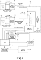
Figure 2 illustrates a device for managing the access, for programming and erase operations, to a memory according to a further aspect of the present invention; -
Figure 3 illustrates, by means of a state diagram, phases of a method for managing the access to the memory, according to one embodiment of the present invention; and -
Figures 4A-4D show examples of the method for managing the access to the memory, under respective operating conditions. -
Figure 1 illustrates a block diagram of a module 1 for managing the access to amemory 3. The module 1 has the function of interface between a plurality of processing units (CPUs) 12, 14 and thememory 3. - The
memory 3 is, in particular, of the non-volatile type, even more particularly a memory of the Flash type which, in use, is written (programmed) or erased on the basis of requests coming from theCPU - According to one aspect of the present invention, a programming / erase controller (also known as PEC) 4 is operationally coupled to the
memory 3 in order to execute programming and erase operations for the latter. Thecontroller 4 operates as an interface between theprocessing unit memory 3. Thecontroller 4 is of the programmable type, and is, in particular, configured for executing programming and erase subroutines stored in asupport memory 2 coupled to it for example by means of actuators (in other words interface registers) 5, in a manner known per se. Theactuators 5 are, in particular, registers that contain control bits which act directly on the circuit blocks of thememory 3. They operate for example so as to address a specific column and row of thememory array 3, to enable a reference voltage in devices for reading thememory 3, to enable a voltage higher than the standard one in row and column decoders of thememory 3, to enable the generation of the programming or erase pulse within the selected memory cells, etc. - Furthermore, a
pointer memory 6, operationally coupled to thecontroller 4, cooperates with thecontroller 4 in order to control the access to specific areas of thesupport memory 2 on the basis of pointers stored in thepointer memory 6. - The
support memory 2 is of the volatile type (e.g. a RAM) and contains the data block and the instructions, in machine language, interpreted and executed by thecontroller 4 in order to manage the access to thememory 3 in programming and erase operations. - The operations for programming/erasing a memory take place in a manner known per se and thus are not described in detail here.
- The module 1 furthermore includes a
first register block 8 and asecond register block 10, configured for storing requests for writing and erasing thememory 3 coming from thefirst CPU 12 and, respectively, from thesecond CPU 14. For this purpose, therefore, thefirst register block 8 is configured so as to be coupled to thefirst CPU 12, whereas thesecond register block 10 is configured so as to be coupled to thesecond CPU 14. The first and thesecond register blocks memory 3 for the completion of the aforementioned programming / erase operations. This state information is, for example, of the binary type, in which a first value identifies the completion of the programming / erase operation, and a second value indicates that the programming / erase operation has not yet been completed. The first and thesecond CPU second register blocks memory 3. - A memory management and
control block 15 forms an interface for the exchange of data between the first and thesecond CPU memory 2. More particularly, the memory management andcontrol block 15 is interfaced with the first and thesecond register block CPU control block 15 is interfaced with thecontroller 4, to which it sends the boot commands for the programming / erase operations on thememory 3 and from which it receives information relating to the execution of the programming / erase operations on thememory 3 stored in thesupport memory 2. - Furthermore, the memory management and
control block 15 is responsible for reserving the space in thememory 2 for storing all the information useful for the write (programming) phase of thememory 3. In this context, thepointer memory 6 stores the physical addresses of thesupport memory 2, in such a manner that thecontroller 4 has this information available both at the start of the programming operation and during the programming operation itself (updated address). Thecontroller 4 can, accordingly, access the programming and erase subroutines stored in thepointer memory 2, interrupt the execution of this subroutine and resume the execution of the subroutine from the point of the previous interruption, according to needs and as better illustrated in the following. - The information relating to the
memory address 3 in which the programming operation is taking place and the address of thememory 2 relating to the subroutine which is being executed by thecontroller 4, are therefore useful for suspending and, successively, resuming the programming operation. - In an analogous manner, the
pointer memory 6 stores both the physical addresses of thememory 3 and the data relating to the subroutine of thememory 2, for the operation for erasing the data under the control of thefirst CPU 12 or of thesecond CPU 14. Also, in this case, the information relating to the memory address in which the erase operation is taking place, together with the pointers to the subroutine in thememory 2 are useful for suspending and, subsequently, resuming the erase operation. - In use, both the first and the
second CPU memory 3. In an analogous manner, requests for programming/erasing thememory 3 may arrive at thememory control block 16 from one of the first or thesecond CPU second CPU memory 3. - According to one aspect of the present invention, a method is provided for managing the requests for accessing the
memory 3, for the programming and erase phases of the latter, that is transparent to the first and to thesecond CPU memory 3, coming from the first and from thesecond CPU memory 3 is busy. - For this purpose, with reference to
Figure 2 , the memory management andcontrol block 15 includes a memorycontrol interface block 16 and aconflict management block 20, operationally coupled together, and whose operation is described with reference to the state machine inFigure 3 . - Basically, in order to implement a method for managing the conflicts, the device 1 is configured for: associating, with operations executed by the
first CPU 12, a priority for access to thememory 3 which is different from the access priority associated with operations executed by thesecond CPU 14; commanding, in the absence of any other requests for accessing thememory 3, the access to thememory 3 for one of thefirst CPU 12 and thesecond CPU 14 that was the first to send a first access request; verifying (e.g. by comparison means), following a receipt of a second access request by the other of thefirst CPU 12 and thesecond CPU 14, the access priority associated with this second access request; suspending (in a manner that is transparent to the first andsecond CPU 12, 14) one of the first or the second access request; and, authorizing the other of the first or the second access request. The suspension and the authorization of the access to thememory 3 is based on a comparison between the priorities associated with the various requests. For example, the access request associated with a lower priority value is suspended compared with the access request associated with a higher priority value. - The method for managing the conflicts executed by the memory management and
control block 15 is here described in detail in the following with joint reference toFigures 2 and3 . - The
conflict management block 20 will be, in an initial phase in which there are no requests for programming or erasing thememory 3 by the first or by thesecond CPU - When one of the first or the
second CPU respective register block 8, 10), this request is acquired by thememory control interface 16 and sent to theconflict management block 20, together with the information relating to which of the first or the second CPU has made an request for accessing the memory 3 (thememory control interface 16 is, in fact, aware of the origin of the request for accessing thememory 3 on the basis of the information acquired by theregisters conflict management block 20 thus goes from the wait state 100 into theinterpreter state 102. - In the
interpreter state 102, theconflict management block 20 verifies whether the programming or erase request originates from thefirst CPU 12 or from thesecond CPU 14. - In the case in which the programming or erase request originates from the
first CPU 12, theconflict management block 20 sends a suitable command to thecontroller 4 and, at the same time, initializes thepointer memory 6 in order to store, and to keep updated, the pointers to the code (stored in the support memory 2) to be executed by means of thecontroller 4, throughout the whole operation for programming or erasing thememory 3. Thepointer memory 6 includes, for this purpose, afirst pointer 6a to thememory 2 dedicated to the operations of thefirst CPU 12 and asecond pointer 6b to thememory 2 dedicated to the operations of thesecond CPU 14. - Simultaneously with the start of the programming / erase operations on the
memory 3 requested by thefirst CPU 12, a first flag (e.g. a binary value) is enabled which identifies a state of being or not being in the operating condition for programming / erasing thememory 3 under the control of the first CPU 12 (for example, setting the first flag to a logic value "1" or "0", where "1" identifies an active access request and "0" identifies no active access request). The first flag may for example be stored in a memory (not shown) internal to theconflict management block 20. - The system thus goes into a state for controlling the
access 104 to thememory 3, in order to carry out the programming or erase operations requested by thefirst CPU 12. When the programming and erase operations on thememory 3 are finished, it returns to theinterpreter state 102. - According to one aspect of the present invention, however, during the execution of the programming and erase operations (state 104), the
conflict management block 20 remains in a wait state in order to acquire potential commands coming from thememory control interface 16, relating to requests for accessing thememory 3 coming from thesecond CPU 14. In the case in which thesecond CPU 14 makes a request for accessing thememory 3 for a programming or erase operation, the start of atimer 24, coupled to theconflict management block 20, is triggered which limits the time spent in thestate 104. In this phase, the request for accessing thememory 3 from thesecond CPU 14 is put into a state of suspension in a manner that is transparent to thesecond CPU 14. In other words, the request for accessing thememory 3 made by thesecond CPU 14 is accepted (but temporarily suspended) also in the presence of a "memory busy" (currently used by the first CPU 12). There is therefore only a delay in the operation for access to thememory 3 by thesecond CPU 14, given substantially by the duration of the interval defined by thetimer 24. Thetimer 24 is, advantageously, of the programmable type, in order to be able to modify, according to needs and as a function of the area of application, the duration of the time interval to be scanned. - When the
timer 24 reaches a predefined threshold value (e.g., in the case of the timer counting down, the threshold could be the value 0), the output goes out of thestate 104 and into afirst arbitration state 106. In the case in which, when thetimer 24 reaches the threshold, the programming or erase operations requested by thefirst CPU 12 have not been completed, these operations are suspended in a safe manner (in other words, in the absence of loss of data - in a manner known per se and not a subject of the present invention). Thecontroller 4 is responsible for carrying out the safe suspension operation. However, according to one aspect of the present invention, beyond the suspension of the abovementioned operations, the address of thememory 2 relating to the subroutine specific to the management of the operation in question is also stored in thefirst pointer 6a, together with the address of thememory 2 that contains all the parameters useful to the execution of the operation in question (e.g. address of thememory 3, type of operation from between programming and erase, pointer to a specific phase of the operation in question, etc.), in order to be able to resume, at a later time, the programming / erase operations whenever the latter have been interrupted. - In the
first arbitration state 106, theconflict management block 20 verifies whether the suspension of the programming / erase operations of thefirst CPU 12 has taken place under external control (for example, the user has voluntarily cancelled these operations), or else has been requested following the expiration of the timer 24 (timeout). In the first case (voluntary suspension by the user), it returns to theinterpreter state 102 and the first flag signalling the request for accessing thememory 3 by thefirst CPU 12 is set at the logic value "0" (no active request for accessing the memory). In the second case (suspension through timeout), it goes to a state for controlling theaccess 108 in order to carry out the programming or erase operations requested by thesecond CPU 14, and the first flag signalling the request for accessing thememory 3 by thefirst CPU 12 is held at the logic value "1" (active request for accessing the memory). - The state for controlling the
access 108 is analogous to the state for controlling theaccess 104 but identifies, in this context, operations executed on thememory 3 by thesecond CPU 14. During the execution of the access to thememory 3 for the programming and erase operations requested by the second CPU 14 (state 108), theconflict management block 20 remains in a wait state so as to acquire potential commands (coming from the memory control interface 16) relating to requests for accessing thememory 3 coming from thefirst CPU 12. In the case in which the transition from theaccess control state 104 to theaccess control state 108 has occurred following a suspension through timeout, the first flag (which signals the request for accessing thememory 3 from the first CPU 12) is held at the logic value "1" (thefirst CPU 12 has not completed the operations on the memory 3). - Simultaneously with the start of the programming / erase operations on the
memory 3 requested by thesecond CPU 14, a second flag (e.g. a binary value) is enabled that identifies a state of being or not being in the operating condition for programming / erasing thememory 3 under the control of the second CPU 14 (for example, setting the second flag at logic value "1" or "0", where "1" identifies an active access request and "0" identifies no active access request). The second flag may for example be stored in the memory internal to theconflict management block 20, in a similar manner to the first flag. - The time spent in the
access control state 108 is, in this case, defined by a respective time interval set by means of thetimer 24, which limits the time spent in thestate 108. When thetimer 24 reaches a predefined threshold value (e.g. in the case of counting down the threshold could be the value 0), the output goes fromstate 108 and to asecond arbitration state 110. In the case in which, when thetimer 24 reaches the threshold, the programming or erase operations requested by thesecond CPU 14 have not been completed, these operations are suspended in a safe manner (in other words, in the absence of loss of data - in a manner known per se). Accordingly, in this case, thecontroller 4 is responsible for carrying out the safe suspension operation. According to one aspect of the present invention, other than the suspension of the aforementioned operations, the address of thememory 2 relating to the specific subroutine for management of the operation in question, and the address of thememory 2 that contains all the parameters useful to the execution of the operation in question (e.g. address of thememory 3, type of operation between programming and erase, pointer to the phase of the operation in question, etc.) are also stored in thesecond pointer 6b, in order to be able to resume the programming / erase operations, at a later time, from the address at which the latter had been interrupted. The second flag is held at the value "1" (active request for accessing the memory). - In the
second arbitration state 110, theconflict management block 20 verifies whether the suspension of the programming / erase operations of thesecond CPU 14 has taken place under an external control (for example, the user has voluntarily cancelled these operations), or else has been requested subsequent to the expiration of the timer 24 (timeout). In the first case (voluntary suspension by the user), it returns to theinterpreter state 102 and the second flag is set to the value "0" (no request for accessing the memory). In the second case (suspension through timeout), it returns to the state for controlling theaccess 104 in order to resume the programming or erase operations previously requested by thefirst CPU 12 and temporarily suspended, and the second flag is held at the value "1". The programming or erase operation requested by thefirst CPU 12 is resumed from the address stored in thefirst pointer 6a. - In an similar manner to what has been described for the transition from the
access control state 104 to theaccess control state 108, also in this case the second flag at the value "1" identifies a state of suspension of the operations requested by thesecond CPU 14 and, accordingly, thetimer 24 is activated in a similar manner to what has been previously described. - It is clear that, in the case in which the
conflict management block 20 is in the wait state 100 or in theinterpreter state 102, and it receives a request for accessing thememory 3 from thesecond CPU 14, it goes from theinterpreter state 102 to the state for controllingaccess 108, maintaining a monitoring for a potential request, from thefirst CPU 12, for accessing the memory. In the latter case, thetimer 24 is activated and the transition from one state to another is carried out according to what has already previously been described. - In the absence of requests for accessing the
memory 3, monitored in theinterpreter state 102, the system returns to the wait state 100. - There is accordingly a timed access to the
memory 3 in order to carry out both the operations requested by thefirst CPU 12 and the operations requested by thesecond CPU 14, within respective alternate intervals of time. The access to thememory 3 is, in other words, guaranteed for both the first and thesecond CPU memory 3 is transparent to the first and to thesecond CPU memory 3 are always accepted by thememory control interface 16, and the management of the time-sharing mechanism is requested from theconflict management block 20. - According to one aspect of the present disclosure, the
first CPU 12 is a main CPU, whereas thesecond CPU 14 is a secondary or auxiliary CPU; the main CPU and the secondary CPU are associated with different access priorities to thememory 3. - In order to manage appropriately the different access priorities to the
memory 3, it is possible to program thetimer 24 in such a manner as to associate with the operations (programming or erase) requested by the first CPU 12 a time interval that is longer compared with the corresponding time interval allocated to the operations (programming or erase) requested by thesecond CPU 14. - Furthermore, or alternatively, it is possible to manage the programming operations in a manner different from the operations for erasing the
memory 3. For example, according to one aspect of the present disclosure, the programming operations requested by the first CPU 12 (main CPU), are always completed, even in the case where the second (secondary)CPU 14 makes a request for accessing thememory 3. In this case, thetimer 24 is not activated. On the contrary, the erase operations requested by the first CPU 12 (main CPU) are suspended (by countdown means with a timer 24) in the case in which the second (secondary)CPU 14 makes a request for accessing thememory 2. - In a similar manner, it is possible to set the state machine in
Figure 3 in such a manner that the programming operations requested by the second CPU 14 (secondary CPU) are always completed, even in the case in which the first (main)CPU 12 makes a request for accessing thememory 3. In this case, thetimer 24 is not activated. Instead, the erase operations requested by the second (secondary)CPU 14 are suspended (by countdown means with a timer 24) in the case in which the first (main)CPU 12 makes a request for accessing thememory 3. - The management and the programming of the
timer 24 is however free and may be modified according to the operating environment and to the specific needs required by the specific application. - The management of the access to the
memory 3 by the first and by thesecond CPU second CPU phase 104 inFigure 3 , a decision phase (e.g. operation for comparison of the priorities associated with the requests for accessing the memory 3) is carried out in order to define the successive operations for activation of thetimer 24 and/or for transition to thearbitration phase 106. Similarly, also in thephase 104 inFigure 3 , a decision phase (e.g. operation for comparison of the priorities associated with the requests for accessing the memory 3) is carried out in order to define the successive operations for activation of thetimer 24 and/or for transition to thearbitration phase 110. - For example, in the case in which the operation is in the
phase 108 and a request for accessing the memory is received from the first CPU (main CPU, whose access requests have a higher priority compared with the access requests from the secondary CPU), thetimer 24 is reset to a value "N" (e.g. 5 ms), in order to carry out the safe suspension of the operations executed by the second CPU. In contrast, still in the framework of the example in question here, in the case in which the operation is in thephase 104 and a request for accessing the memory is received from the second CPU (secondary CPU, whose access requests have a lower priority compared with the access requests from the main CPU), thetimer 24 is reset to a higher value of "N", e.g. "10N" (here, 50 ms) and the forced suspension of the operations executed by the first CPU is carried out. -
Figures 4A-4D illustrate examples of management of the timing of the programming and erase phases of thememory 3, in a manner that is transparent to the first and to thesecond CPU memory 3. -
Figure 4A illustrates an operating condition in which thefirst CPU 12 has made a request for programming thememory 3 at the time t0, in the absence of previous or concomitant requests from thesecond CPU 14. The programming phase of thememory 3 is thus initiated, in a manner known per se. At the time t1>t0, during the programming of thememory 3 by thefirst CPU 12, thesecond CPU 14 requests the access to thememory 3 for a programming phase. In this example, the programming is completed without starting thetimer 24. The request by thesecond CPU 14 is put into a state of temporary suspension. At the time t2, the programming is terminated, and it is thus possible to start the programming of thememory 3 by thesecond CPU 14. -
Figure 4B illustrates an operating condition in which thefirst CPU 12 has made a request for erasing thememory 3 at the time t3, in the absence of previous or concomitant requests from thesecond CPU 14. The erase phase of thememory 3 is thus initiated, in a manner known per se. At the time t4>t3, during the erasing of thememory 3 by thefirst CPU 12, thesecond CPU 14 requests the access to thememory 3 for a programming phase. - In this example, the programming requests from the
second CPU 14 have priority over the erase requests from thefirst CPU 12 and, accordingly, thetimer 24 is activated (countdown time interval Δtc, for example equal to a few milliseconds, e.g. between 4 and 10 ms, in particular 5 ms). The request by thesecond CPU 14 is put into a state of temporary suspension. At the time t5=t4+Δtc, the erase phase controlled by thefirst CPU 12 is suspended and the programming of thememory 3 by thesecond CPU 14 is started. - In this example, the phase for programming the
memory 3 by thesecond CPU 14 has absolute priority over the phase for erasing thememory 3 by thefirst CPU 12 and, accordingly, the programming is taken to completion without starting thetimer 24. The programming phase terminates at the time t6. It is thus possible to restart the erase phase of thememory 3 previously suspended, as illustrated at the time t6+5 (where δ represents a generic delay, e.g. computational, for the transition from one operating condition to another). -
Figure 4C illustrates an operating condition in which thesecond CPU 14 has made a request for programming thememory 3 at the time t7, in the absence of previous or concomitant requests from thefirst CPU 12. The programming phase of thememory 3 is thus initiated, in a manner known per se. At the time t8>t7, during the programming of thememory 3 by thesecond CPU 14, thefirst CPU 12 requests the access to thememory 3 for an erase phase. In this example, the erase requests coming from thefirst CPU 12 do not have absolute priority over the programming requests coming from thesecond CPU 14 and, accordingly, the programming is taken to completion without thetimer 24 being started. The request by thefirst CPU 12 is put into a state of temporary suspension. At the time t9, the programming is terminated, and it is thus possible to start the erasing thememory 3 by thefirst CPU 12. -
Figure 4D illustrates one operating condition in which thesecond CPU 14 has made a request for erasing thememory 3 in the absence of previous or concomitant requests from thefirst CPU 12. The erase phase of thememory 3 is thus initiated, in a manner known per se. At the time t10, during the erasing of thememory 3 by thesecond CPU 14, thefirst CPU 12 requests the access to thememory 3 for a programming phase. - The
timer 24 is activated (countdown time interval Δtc, for example equal to 5ms) in order to allow thefirst CPU 12 to access thememory 3 with a predefined maximum delay (here, Δtc). The request by thefirst CPU 12 is put into a state of temporary suspension. At the time t11=t10+Δtc, the erase phase controlled by thesecond CPU 14 is suspended and the programming of thememory 3 by thefirst CPU 12 is triggered. - In this example, the programming phase of the
memory 3 by thefirst CPU 12 has absolute priority over the erase phase of thememory 3 by thesecond CPU 14 and, accordingly, at the time t11, thetimer 24 is activated. Thememory 3 remains dedicated to thefirst CPU 12 for the entire time defined by thetimer 24, in this example for the time interval Δtp (for example equal to a few tens of milliseconds, e.g. between 30 and 70 ms, in particular 50 ms). Here, the programming is ended at the time t12, before the end of the time interval Δtp. The system therefore remains in a wait state for further programming commands coming from thefirst CPU 12, in the presence of which a new programming of thememory 3 begins (e.g. restarting thetimer 24 with an interval Δtp or with a different interval, or else disabling it and bringing the potential further programming phase to an end). - At the end of the time Δtp, and in the absence of further programming commands coming from the first CPU 12 (time t13), the erase operation on the
memory 3, commanded by thesecond CPU 14 and previously suspended, is restarted (time t13+δ where δ is the delay for the transition from one operating condition to another). - The advantages offered by the present invention will be apparent from the preceding description. In particular, the invention previously described provides for the controller block 4 (PEC) to be of the programmable type, and for the other blocks (
e.g. control interface 16 and conflict management block 20) to be configurable and able to be modified according to needs in order to adapt them to application contexts that are different from one to another. - The programmability of the
controller 4, which operates as an interface for the programming of thememory 3, allows corrections and software patches to be implemented in a quick and efficient manner. - Furthermore, the solution provided does not require the use of an interrupt controller. Moreover, the module 1 according to the present solution does not require modifications either to the memory or to the CPU that access this memory, and its operation is transparent to both.
- Finally, it is clear that modifications and variants may be applied to the invention described and illustrated here without however straying from the scope of protection of the present invention, as defined in the appended claims.
- For example, the module 1 may be configured in such a manner as to e coupled to any given number of CPUs, greater than two. In this case, it is appropriate to provide a respective number of input registers (analogous to the
registers 8 and 10), each of them being dedicated to a respective CPU. Theconflict management block 20 is, in this case, programmed to manage the access requests from all the CPUs within respective non-overlapping intervals of time, in a similar manner to what has been previously described.
Claims (24)
- Interface module (1) for managing operations for accessing a Flash memory (3) requested by a main processing unit (12) and by an auxiliary processing unit (14), comprising:- a first register block (8), couplable to the main processing unit (12), configured for storing requests for accessing the Flash memory (3) coming from the main processing unit (12);- a second register block (10), couplable to the auxiliary processing unit (14), configured for storing respective requests for accessing the Flash memory (3) coming from the auxiliary processing unit (14);- a conflict management unit (20), coupled to the first register block (8) and to the second register block (10) for receiving said requests for accessing the Flash memory (3),
in which is associated with the access requests coming from the main processing unit (12), in at least one operating condition, a first access priority to the Flash memory (3) which is different from a second access priority to the Flash memory (3) associated with the access requests coming from the auxiliary processing unit (14),
said conflict management unit (20) being configured for:• following a receipt of a first request for accessing the Flash memory (3) by one of the main and auxiliary processing unit, and in the absence of further requests for accessing the Flash memory (3), command (104; 108) the access to the Flash memory (3) for the main or auxiliary processing unit (12, 14) which has initiated this first access request;• following a receipt of a second request for accessing the Flash memory (3) from the other of the main and auxiliary processing unit, during the access to the Flash memory (3) of the main or auxiliary processing unit (12, 14) which has initiated the first access request, compare (104; 108) the access priority associated with the first access request with the access priority associated with the second access request;• on the basis of a result of said comparison, suspend (106; 110) one of the first or the second access request; and• authorize (104; 108) the other of the first or the second access request. - Interface module according to Claim 1, in which the conflict management unit (20) includes:- a support memory (2), configured for storing programming and erase subroutines for the Flash memory (3);- a programming / erase controller, PEC, (4), coupled to the support memory (2), controllable for programming or erasing blocks of the Flash memory (3) by executing said programming or erase subroutine, said PEC (4) being of the programmable type.
- Interface module according to Claim 2, furthermore comprising a first pointer block (6a), coupled to the PEC (4), configured for storing, when is suspended (106; 110) the first access request, a first address of the support memory (2) associated with the programming or erase subroutine executed by the PEC (4) upon a request by the main (12) or auxiliary processing unit (14) which has generated the first access request.
- Interface module according to Claim 3, in which the first pointer block (6a) is furthermore configured for storing, when the first access request is suspended (106; 110), a third address of the support memory (2) that contains a respective address to the block of the Flash memory (3) corresponding to which one of a programming or erase operation is being executed, requested by the main processing unit (12) or auxiliary processing unit processing unit (14) which has generated the first access request.
- Interface module according to any one of Claims 2-4, furthermore comprising a second pointer block (6b), coupled to the PEC (4), configured for storing, when the second access request is suspended (106; 110), a second address of the support memory (2) associated with the programming or erase subroutine executed by the PEC (4) upon a request from the main processing unit (12) or auxiliary processing unit processing unit (14) which has generated the second access request.
- Interface module according to Claim 5, in which the second pointer block (6b) is furthermore configured for storing, when the second access request is suspended (106; 110), a fourth address of the support memory (2) which contains a respective address to the block of the memory (3) corresponding to which one of a programming or erase operation is being executed, requested by the main processing unit (12) or auxiliary processing unit processing unit (14) which has generated the second access request.
- Interface module according to Claims 3 to 6, in which said conflict management unit (20) is configured for suspending and resuming the programming or erase subroutine executed by the PEC (4) using the first, the second, the third and the fourth address of the support memory (2).
- Interface module according to any one of the preceding claims, furthermore comprising a timer (24), coupled to the conflict management unit (20), configured for defining a time interval before proceeding with the suspension (106; 110) of said one of the first or the second access request.
- Interface module according to any one of the preceding claims, in which the first and the second request for accessing the Flash memory (3) include a request for programming blocks of the Flash memory (3) and a request for erasing blocks of the Flash memory (3).
- Interface module according to Claim 9, in which the request for programming blocks of the Flash memory (3) is associated with a higher access priority to the Flash memory (3) compared with the access priority with which the request for erasing blocks of the Flash memory (3) is associated.
- Interface module according to Claim 2, in which the PEC (4) and the support memory (2) cooperate in such a manner that the programming operation is always brought to completion before carrying out the erase operation.
- Interface module according to any one of the preceding claims, in which the access priority associated with the first access request is higher than the access priority associated with the second access request,
the suspension (106; 110) of the first or of the second access request comprising the suspension of the access request having lower priority. - Method for managing operations for accessing a Flash memory (3) on the basis of requests received from a main processing unit (12) and from an auxiliary processing unit (14), comprising the phases for:- storing, in a first register block (8), requests for accessing the Flash memory (3) coming from the main processing unit (12);- storing, in a second register block (10), requests for accessing the Flash memory (3) coming from the auxiliary processing unit (14);- associating, with access requests coming from the main processing unit (12), a first access priority to the Flash memory (3) which is different from a second access priority to the Flash memory (3) associated with the access requests coming from the auxiliary processing unit (14);- commanding (104; 108), following a receipt of a first request for accessing the Flash memory (3) from one of the main and auxiliary processing unit (12, 14) and in the absence of further requests for accessing the Flash memory (3), the access to the Flash memory (3) of the main or auxiliary processing unit (12, 14) which has initiated this first access request;- comparing (104; 108), following a receipt of a second request for accessing the Flash memory (3) from the other of the main and auxiliary processing unit during the access to the Flash memory (3) of the main or auxiliary processing unit (12, 14) which has initiated the first access request, the access priority associated with the first access request with the access priority associated with the second access request;- suspending (106; 110), on the basis of a result of said comparison, one of the first or the second access request; and- authorizing (104; 108) the other of the first or the second access request.
- Method according to Claim 13, furthermore comprising the phases for:- storing, in a support memory (2), subroutines for programming and erasing the Flash memory (3); and- programming or erasing blocks of the Flash memory (3) by executing said programming or erase subroutine by means of a programming / erase controller, PEC, (4) coupled to the support memory (2).
- Method according to Claim 14, furthermore comprising the phase for storing, when the first access request is suspended (106; 110), a first address of the support memory (2) associated with the programming or erase subroutine executed by the PEC (4) upon a request from the main processing unit (12) or auxiliary processing unit (14) which has generated the first access request.
- Method according to Claim 15, furthermore comprising the phase for storing, when the first access request is suspended (106; 110), a third address of the support memory (2) which contains a respective address to the block of the Flash memory (3) corresponding to which one of a programming or erase operation is being executed, requested by the main processing unit (12) or auxiliary processing unit (14) which has generated the first access request.
- Method according to either of Claims 15 and 16, furthermore comprising the phase for storing, when the second access request is suspended (106; 110), a second address of the support memory (2) associated with the programming or erase subroutine executed by the PEC (4) upon a request from the main processing unit (12) or auxiliary processing unit (14) which has generated the second access request.
- Method according to Claim 17, furthermore comprising the phase for storing, when the second access request is suspended (106; 110), a fourth address of the support memory (2) which contains a respective address to the block of the Flash memory (3) corresponding to which one of a programming or erase operation is being executed, requested by the main processing unit (12) or auxiliary processing unit (14) which has generated the second access request.
- Method according to Claims 15 to 18, furthermore comprising the phase for suspending and resuming the programming or erase subroutine using the first, the second, the third and the fourth address of the support memory (2).
- Method according to any one of Claims 13 to 19, furthermore comprising the phase for defining a time interval prior to carrying out the suspension (106; 110) of said one of the first or the second access request.
- Method according to any one of Claims 13 to 20, in which the first and the second request for accessing the Flash memory (3) include a request for programming blocks of the Flash memory (3) and a request for erasing blocks of the Flash memory (3).
- Method according to Claim 21, furthermore comprising the phase for associating, with the request for programming blocks of the Flash memory (3) and with the request for erasing blocks of the Flash memory (3), a respectively higher and lower access priority.
- Method according to Claim 22, furthermore comprising the phase for commanding a programming / erase controller, PEC, (4) in such a manner that the programming operation is always brought to completion before carrying out the erase operation.
- Method according to any one of Claims 13 to 23, in which the access priority associated with the first access request is higher than the access priority associated with the second access request,
the phase for suspending (106; 110) the first or the second access request comprising the suspension of the access request having lower priority.
Applications Claiming Priority (1)
| Application Number | Priority Date | Filing Date | Title |
|---|---|---|---|
| IT102017000034731A IT201700034731A1 (en) | 2017-03-29 | 2017-03-29 | MODULE AND METHOD OF MANAGEMENT OF ACCESS TO A MEMORY |
Publications (2)
| Publication Number | Publication Date |
|---|---|
| EP3382566A1 true EP3382566A1 (en) | 2018-10-03 |
| EP3382566B1 EP3382566B1 (en) | 2020-03-04 |
Family
ID=59521571
Family Applications (1)
| Application Number | Title | Priority Date | Filing Date |
|---|---|---|---|
| EP18163468.4A Active EP3382566B1 (en) | 2017-03-29 | 2018-03-22 | Module and method for managing the access to a memory |
Country Status (3)
| Country | Link |
|---|---|
| US (2) | US10387334B2 (en) |
| EP (1) | EP3382566B1 (en) |
| IT (1) | IT201700034731A1 (en) |
Families Citing this family (1)
| Publication number | Priority date | Publication date | Assignee | Title |
|---|---|---|---|---|
| CN116194904A (en) | 2021-03-29 | 2023-05-30 | 华为技术有限公司 | Method and device for accessing flash memory |
Citations (2)
| Publication number | Priority date | Publication date | Assignee | Title |
|---|---|---|---|---|
| GB2488516A (en) * | 2011-02-15 | 2012-09-05 | Advanced Risc Mach Ltd | Using priority dependent delays to ensure that the average delay between accesses to a memory remains below a threshold |
| US20140281283A1 (en) * | 2013-03-13 | 2014-09-18 | Qualcomm Incorporated | Dual host embedded shared device controller |
Family Cites Families (5)
| Publication number | Priority date | Publication date | Assignee | Title |
|---|---|---|---|---|
| KR100725417B1 (en) * | 2006-02-22 | 2007-06-07 | 삼성전자주식회사 | Apparatus and Method for Computing Flash Memory According to Priority |
| JP5243711B2 (en) * | 2006-11-10 | 2013-07-24 | セイコーエプソン株式会社 | Processor |
| JP4612710B2 (en) * | 2008-06-02 | 2011-01-12 | 株式会社日立製作所 | Transaction parallel control method, database management system, and program |
| US9606833B2 (en) * | 2014-04-09 | 2017-03-28 | Samsung Electronics Co., Ltd | Method and apparatus for providing a preemptive task scheduling scheme in a real time operating system |
| US20160054779A1 (en) * | 2014-08-22 | 2016-02-25 | Devadatta Bodas | Managing power performance of distributed computing systems |
-
2017
- 2017-03-29 IT IT102017000034731A patent/IT201700034731A1/en unknown
- 2017-10-30 US US15/797,940 patent/US10387334B2/en active Active
-
2018
- 2018-03-22 EP EP18163468.4A patent/EP3382566B1/en active Active
-
2019
- 2019-06-27 US US16/455,155 patent/US10901919B2/en active Active
Patent Citations (2)
| Publication number | Priority date | Publication date | Assignee | Title |
|---|---|---|---|---|
| GB2488516A (en) * | 2011-02-15 | 2012-09-05 | Advanced Risc Mach Ltd | Using priority dependent delays to ensure that the average delay between accesses to a memory remains below a threshold |
| US20140281283A1 (en) * | 2013-03-13 | 2014-09-18 | Qualcomm Incorporated | Dual host embedded shared device controller |
Also Published As
| Publication number | Publication date |
|---|---|
| IT201700034731A1 (en) | 2018-09-29 |
| US20190317902A1 (en) | 2019-10-17 |
| US10387334B2 (en) | 2019-08-20 |
| US20180285284A1 (en) | 2018-10-04 |
| US10901919B2 (en) | 2021-01-26 |
| EP3382566B1 (en) | 2020-03-04 |
Similar Documents
| Publication | Publication Date | Title |
|---|---|---|
| US20180373655A1 (en) | Controller for a memory system | |
| CN102033790B (en) | Method and device for upgrading embedded-type system BOOTROM | |
| CN100530153C (en) | Apparatus and method for processing operations of nonvolatile memory in order of priority | |
| CN111857814B (en) | Memory controller that executes microinstructions | |
| CN105144096B (en) | Apparatus and method for updating startup code in a microcontroller | |
| US10437623B2 (en) | Fast switching between virtual machines without interrupt virtualization for high-performance, secure trusted-execution environment | |
| US9552849B2 (en) | Memory device with timing overlap mode and precharge timing circuit | |
| KR20130081508A (en) | Method for controlling memory system when sudden power off occurs | |
| EP3382566B1 (en) | Module and method for managing the access to a memory | |
| JP2008123157A (en) | Processor and interrupt control method | |
| EP3564764B1 (en) | Device for processing programmable logic controller program | |
| KR102235142B1 (en) | Handling time intensive instructions | |
| RU2524570C2 (en) | Electronic control unit having real-time core managing partitioning | |
| TW202008371A (en) | Data processing system and data processing method | |
| JP2000148543A (en) | Method and device for controlling writing of flash eeprom by microcomputer | |
| JP2002297563A (en) | Microcomputer and data processing apparatus | |
| US20160239443A1 (en) | Dma controller | |
| JP2023156549A (en) | semiconductor equipment | |
| US10599589B2 (en) | Semiconductor device and flash-memory control method | |
| JP2015170180A (en) | Electronic control unit | |
| JP6998434B2 (en) | Electronic control device for automobiles | |
| JP6762411B2 (en) | Electronic control unit for automobiles | |
| JP2009110150A (en) | Semiconductor device and method of operating semiconductor device | |
| KR102339278B1 (en) | How Calculation Units Work | |
| US11048575B2 (en) | Method and device for error handling in a communication between distributed software components |
Legal Events
| Date | Code | Title | Description |
|---|---|---|---|
| PUAI | Public reference made under article 153(3) epc to a published international application that has entered the european phase |
Free format text: ORIGINAL CODE: 0009012 |
|
| STAA | Information on the status of an ep patent application or granted ep patent |
Free format text: STATUS: THE APPLICATION HAS BEEN PUBLISHED |
|
| AK | Designated contracting states |
Kind code of ref document: A1 Designated state(s): AL AT BE BG CH CY CZ DE DK EE ES FI FR GB GR HR HU IE IS IT LI LT LU LV MC MK MT NL NO PL PT RO RS SE SI SK SM TR |
|
| AX | Request for extension of the european patent |
Extension state: BA ME |
|
| STAA | Information on the status of an ep patent application or granted ep patent |
Free format text: STATUS: REQUEST FOR EXAMINATION WAS MADE |
|
| 17P | Request for examination filed |
Effective date: 20190318 |
|
| RBV | Designated contracting states (corrected) |
Designated state(s): AL AT BE BG CH CY CZ DE DK EE ES FI FR GB GR HR HU IE IS IT LI LT LU LV MC MK MT NL NO PL PT RO RS SE SI SK SM TR |
|
| GRAP | Despatch of communication of intention to grant a patent |
Free format text: ORIGINAL CODE: EPIDOSNIGR1 |
|
| STAA | Information on the status of an ep patent application or granted ep patent |
Free format text: STATUS: GRANT OF PATENT IS INTENDED |
|
| RIC1 | Information provided on ipc code assigned before grant |
Ipc: G06F 13/16 20060101AFI20190809BHEP |
|
| INTG | Intention to grant announced |
Effective date: 20190828 |
|
| GRAS | Grant fee paid |
Free format text: ORIGINAL CODE: EPIDOSNIGR3 |
|
| GRAJ | Information related to disapproval of communication of intention to grant by the applicant or resumption of examination proceedings by the epo deleted |
Free format text: ORIGINAL CODE: EPIDOSDIGR1 |
|
| GRAL | Information related to payment of fee for publishing/printing deleted |
Free format text: ORIGINAL CODE: EPIDOSDIGR3 |
|
| STAA | Information on the status of an ep patent application or granted ep patent |
Free format text: STATUS: REQUEST FOR EXAMINATION WAS MADE |
|
| GRAR | Information related to intention to grant a patent recorded |
Free format text: ORIGINAL CODE: EPIDOSNIGR71 |
|
| STAA | Information on the status of an ep patent application or granted ep patent |
Free format text: STATUS: GRANT OF PATENT IS INTENDED |
|
| GRAA | (expected) grant |
Free format text: ORIGINAL CODE: 0009210 |
|
| STAA | Information on the status of an ep patent application or granted ep patent |
Free format text: STATUS: THE PATENT HAS BEEN GRANTED |
|
| INTC | Intention to grant announced (deleted) | ||
| AK | Designated contracting states |
Kind code of ref document: B1 Designated state(s): AL AT BE BG CH CY CZ DE DK EE ES FI FR GB GR HR HU IE IS IT LI LT LU LV MC MK MT NL NO PL PT RO RS SE SI SK SM TR |
|
| INTG | Intention to grant announced |
Effective date: 20200124 |
|
| REG | Reference to a national code |
Ref country code: GB Ref legal event code: FG4D |
|
| REG | Reference to a national code |
Ref country code: CH Ref legal event code: EP |
|
| REG | Reference to a national code |
Ref country code: AT Ref legal event code: REF Ref document number: 1241195 Country of ref document: AT Kind code of ref document: T Effective date: 20200315 |
|
| REG | Reference to a national code |
Ref country code: DE Ref legal event code: R096 Ref document number: 602018002779 Country of ref document: DE |
|
| REG | Reference to a national code |
Ref country code: IE Ref legal event code: FG4D |
|
| PG25 | Lapsed in a contracting state [announced via postgrant information from national office to epo] |
Ref country code: NO Free format text: LAPSE BECAUSE OF FAILURE TO SUBMIT A TRANSLATION OF THE DESCRIPTION OR TO PAY THE FEE WITHIN THE PRESCRIBED TIME-LIMIT Effective date: 20200604 Ref country code: RS Free format text: LAPSE BECAUSE OF FAILURE TO SUBMIT A TRANSLATION OF THE DESCRIPTION OR TO PAY THE FEE WITHIN THE PRESCRIBED TIME-LIMIT Effective date: 20200304 Ref country code: FI Free format text: LAPSE BECAUSE OF FAILURE TO SUBMIT A TRANSLATION OF THE DESCRIPTION OR TO PAY THE FEE WITHIN THE PRESCRIBED TIME-LIMIT Effective date: 20200304 |
|
| REG | Reference to a national code |
Ref country code: NL Ref legal event code: MP Effective date: 20200304 |
|
| PG25 | Lapsed in a contracting state [announced via postgrant information from national office to epo] |
Ref country code: GR Free format text: LAPSE BECAUSE OF FAILURE TO SUBMIT A TRANSLATION OF THE DESCRIPTION OR TO PAY THE FEE WITHIN THE PRESCRIBED TIME-LIMIT Effective date: 20200605 Ref country code: HR Free format text: LAPSE BECAUSE OF FAILURE TO SUBMIT A TRANSLATION OF THE DESCRIPTION OR TO PAY THE FEE WITHIN THE PRESCRIBED TIME-LIMIT Effective date: 20200304 Ref country code: BG Free format text: LAPSE BECAUSE OF FAILURE TO SUBMIT A TRANSLATION OF THE DESCRIPTION OR TO PAY THE FEE WITHIN THE PRESCRIBED TIME-LIMIT Effective date: 20200604 Ref country code: LV Free format text: LAPSE BECAUSE OF FAILURE TO SUBMIT A TRANSLATION OF THE DESCRIPTION OR TO PAY THE FEE WITHIN THE PRESCRIBED TIME-LIMIT Effective date: 20200304 Ref country code: SE Free format text: LAPSE BECAUSE OF FAILURE TO SUBMIT A TRANSLATION OF THE DESCRIPTION OR TO PAY THE FEE WITHIN THE PRESCRIBED TIME-LIMIT Effective date: 20200304 |
|
| REG | Reference to a national code |
Ref country code: LT Ref legal event code: MG4D |
|
| PG25 | Lapsed in a contracting state [announced via postgrant information from national office to epo] |
Ref country code: NL Free format text: LAPSE BECAUSE OF FAILURE TO SUBMIT A TRANSLATION OF THE DESCRIPTION OR TO PAY THE FEE WITHIN THE PRESCRIBED TIME-LIMIT Effective date: 20200304 |
|
| PG25 | Lapsed in a contracting state [announced via postgrant information from national office to epo] |
Ref country code: IS Free format text: LAPSE BECAUSE OF FAILURE TO SUBMIT A TRANSLATION OF THE DESCRIPTION OR TO PAY THE FEE WITHIN THE PRESCRIBED TIME-LIMIT Effective date: 20200704 Ref country code: RO Free format text: LAPSE BECAUSE OF FAILURE TO SUBMIT A TRANSLATION OF THE DESCRIPTION OR TO PAY THE FEE WITHIN THE PRESCRIBED TIME-LIMIT Effective date: 20200304 Ref country code: CZ Free format text: LAPSE BECAUSE OF FAILURE TO SUBMIT A TRANSLATION OF THE DESCRIPTION OR TO PAY THE FEE WITHIN THE PRESCRIBED TIME-LIMIT Effective date: 20200304 Ref country code: SM Free format text: LAPSE BECAUSE OF FAILURE TO SUBMIT A TRANSLATION OF THE DESCRIPTION OR TO PAY THE FEE WITHIN THE PRESCRIBED TIME-LIMIT Effective date: 20200304 Ref country code: EE Free format text: LAPSE BECAUSE OF FAILURE TO SUBMIT A TRANSLATION OF THE DESCRIPTION OR TO PAY THE FEE WITHIN THE PRESCRIBED TIME-LIMIT Effective date: 20200304 Ref country code: PT Free format text: LAPSE BECAUSE OF FAILURE TO SUBMIT A TRANSLATION OF THE DESCRIPTION OR TO PAY THE FEE WITHIN THE PRESCRIBED TIME-LIMIT Effective date: 20200729 Ref country code: LT Free format text: LAPSE BECAUSE OF FAILURE TO SUBMIT A TRANSLATION OF THE DESCRIPTION OR TO PAY THE FEE WITHIN THE PRESCRIBED TIME-LIMIT Effective date: 20200304 Ref country code: ES Free format text: LAPSE BECAUSE OF FAILURE TO SUBMIT A TRANSLATION OF THE DESCRIPTION OR TO PAY THE FEE WITHIN THE PRESCRIBED TIME-LIMIT Effective date: 20200304 Ref country code: SK Free format text: LAPSE BECAUSE OF FAILURE TO SUBMIT A TRANSLATION OF THE DESCRIPTION OR TO PAY THE FEE WITHIN THE PRESCRIBED TIME-LIMIT Effective date: 20200304 |
|
| REG | Reference to a national code |
Ref country code: AT Ref legal event code: MK05 Ref document number: 1241195 Country of ref document: AT Kind code of ref document: T Effective date: 20200304 |
|
| REG | Reference to a national code |
Ref country code: DE Ref legal event code: R097 Ref document number: 602018002779 Country of ref document: DE |
|
| REG | Reference to a national code |
Ref country code: BE Ref legal event code: MM Effective date: 20200331 |
|
| PG25 | Lapsed in a contracting state [announced via postgrant information from national office to epo] |
Ref country code: MC Free format text: LAPSE BECAUSE OF FAILURE TO SUBMIT A TRANSLATION OF THE DESCRIPTION OR TO PAY THE FEE WITHIN THE PRESCRIBED TIME-LIMIT Effective date: 20200304 Ref country code: LU Free format text: LAPSE BECAUSE OF NON-PAYMENT OF DUE FEES Effective date: 20200322 |
|
| PLBE | No opposition filed within time limit |
Free format text: ORIGINAL CODE: 0009261 |
|
| STAA | Information on the status of an ep patent application or granted ep patent |
Free format text: STATUS: NO OPPOSITION FILED WITHIN TIME LIMIT |
|
| PG25 | Lapsed in a contracting state [announced via postgrant information from national office to epo] |
Ref country code: DK Free format text: LAPSE BECAUSE OF FAILURE TO SUBMIT A TRANSLATION OF THE DESCRIPTION OR TO PAY THE FEE WITHIN THE PRESCRIBED TIME-LIMIT Effective date: 20200304 Ref country code: AT Free format text: LAPSE BECAUSE OF FAILURE TO SUBMIT A TRANSLATION OF THE DESCRIPTION OR TO PAY THE FEE WITHIN THE PRESCRIBED TIME-LIMIT Effective date: 20200304 Ref country code: IT Free format text: LAPSE BECAUSE OF FAILURE TO SUBMIT A TRANSLATION OF THE DESCRIPTION OR TO PAY THE FEE WITHIN THE PRESCRIBED TIME-LIMIT Effective date: 20200304 Ref country code: IE Free format text: LAPSE BECAUSE OF NON-PAYMENT OF DUE FEES Effective date: 20200322 |
|
| 26N | No opposition filed |
Effective date: 20201207 |
|
| PG25 | Lapsed in a contracting state [announced via postgrant information from national office to epo] |
Ref country code: PL Free format text: LAPSE BECAUSE OF FAILURE TO SUBMIT A TRANSLATION OF THE DESCRIPTION OR TO PAY THE FEE WITHIN THE PRESCRIBED TIME-LIMIT Effective date: 20200304 Ref country code: BE Free format text: LAPSE BECAUSE OF NON-PAYMENT OF DUE FEES Effective date: 20200331 Ref country code: SI Free format text: LAPSE BECAUSE OF FAILURE TO SUBMIT A TRANSLATION OF THE DESCRIPTION OR TO PAY THE FEE WITHIN THE PRESCRIBED TIME-LIMIT Effective date: 20200304 |
|
| PG25 | Lapsed in a contracting state [announced via postgrant information from national office to epo] |
Ref country code: FR Free format text: LAPSE BECAUSE OF NON-PAYMENT OF DUE FEES Effective date: 20200504 |
|
| REG | Reference to a national code |
Ref country code: CH Ref legal event code: PL |
|
| PG25 | Lapsed in a contracting state [announced via postgrant information from national office to epo] |
Ref country code: CH Free format text: LAPSE BECAUSE OF NON-PAYMENT OF DUE FEES Effective date: 20210331 Ref country code: LI Free format text: LAPSE BECAUSE OF NON-PAYMENT OF DUE FEES Effective date: 20210331 |
|
| PG25 | Lapsed in a contracting state [announced via postgrant information from national office to epo] |
Ref country code: TR Free format text: LAPSE BECAUSE OF FAILURE TO SUBMIT A TRANSLATION OF THE DESCRIPTION OR TO PAY THE FEE WITHIN THE PRESCRIBED TIME-LIMIT Effective date: 20200304 Ref country code: MT Free format text: LAPSE BECAUSE OF FAILURE TO SUBMIT A TRANSLATION OF THE DESCRIPTION OR TO PAY THE FEE WITHIN THE PRESCRIBED TIME-LIMIT Effective date: 20200304 Ref country code: CY Free format text: LAPSE BECAUSE OF FAILURE TO SUBMIT A TRANSLATION OF THE DESCRIPTION OR TO PAY THE FEE WITHIN THE PRESCRIBED TIME-LIMIT Effective date: 20200304 |
|
| PG25 | Lapsed in a contracting state [announced via postgrant information from national office to epo] |
Ref country code: MK Free format text: LAPSE BECAUSE OF FAILURE TO SUBMIT A TRANSLATION OF THE DESCRIPTION OR TO PAY THE FEE WITHIN THE PRESCRIBED TIME-LIMIT Effective date: 20200304 Ref country code: AL Free format text: LAPSE BECAUSE OF FAILURE TO SUBMIT A TRANSLATION OF THE DESCRIPTION OR TO PAY THE FEE WITHIN THE PRESCRIBED TIME-LIMIT Effective date: 20200304 |
|
| GBPC | Gb: european patent ceased through non-payment of renewal fee |
Effective date: 20220322 |
|
| PG25 | Lapsed in a contracting state [announced via postgrant information from national office to epo] |
Ref country code: GB Free format text: LAPSE BECAUSE OF NON-PAYMENT OF DUE FEES Effective date: 20220322 |
|
| PGFP | Annual fee paid to national office [announced via postgrant information from national office to epo] |
Ref country code: DE Payment date: 20250218 Year of fee payment: 8 |