EP3379723A1 - Piezoelectric oscillation device and method for manufacturing same - Google Patents
Piezoelectric oscillation device and method for manufacturing same Download PDFInfo
- Publication number
- EP3379723A1 EP3379723A1 EP16878907.1A EP16878907A EP3379723A1 EP 3379723 A1 EP3379723 A1 EP 3379723A1 EP 16878907 A EP16878907 A EP 16878907A EP 3379723 A1 EP3379723 A1 EP 3379723A1
- Authority
- EP
- European Patent Office
- Prior art keywords
- piezoelectric
- substrate
- oscillation device
- substrate holding
- holding member
- Prior art date
- Legal status (The legal status is an assumption and is not a legal conclusion. Google has not performed a legal analysis and makes no representation as to the accuracy of the status listed.)
- Pending
Links
Images





Classifications
-
- H—ELECTRICITY
- H03—ELECTRONIC CIRCUITRY
- H03H—IMPEDANCE NETWORKS, e.g. RESONANT CIRCUITS; RESONATORS
- H03H3/00—Apparatus or processes specially adapted for the manufacture of impedance networks, resonating circuits, resonators
- H03H3/007—Apparatus or processes specially adapted for the manufacture of impedance networks, resonating circuits, resonators for the manufacture of electromechanical resonators or networks
- H03H3/02—Apparatus or processes specially adapted for the manufacture of impedance networks, resonating circuits, resonators for the manufacture of electromechanical resonators or networks for the manufacture of piezoelectric or electrostrictive resonators or networks
-
- H—ELECTRICITY
- H03—ELECTRONIC CIRCUITRY
- H03B—GENERATION OF OSCILLATIONS, DIRECTLY OR BY FREQUENCY-CHANGING, BY CIRCUITS EMPLOYING ACTIVE ELEMENTS WHICH OPERATE IN A NON-SWITCHING MANNER; GENERATION OF NOISE BY SUCH CIRCUITS
- H03B5/00—Generation of oscillations using amplifier with regenerative feedback from output to input
- H03B5/02—Details
- H03B5/04—Modifications of generator to compensate for variations in physical values, e.g. power supply, load, temperature
-
- H—ELECTRICITY
- H03—ELECTRONIC CIRCUITRY
- H03B—GENERATION OF OSCILLATIONS, DIRECTLY OR BY FREQUENCY-CHANGING, BY CIRCUITS EMPLOYING ACTIVE ELEMENTS WHICH OPERATE IN A NON-SWITCHING MANNER; GENERATION OF NOISE BY SUCH CIRCUITS
- H03B5/00—Generation of oscillations using amplifier with regenerative feedback from output to input
- H03B5/30—Generation of oscillations using amplifier with regenerative feedback from output to input with frequency-determining element being electromechanical resonator
- H03B5/32—Generation of oscillations using amplifier with regenerative feedback from output to input with frequency-determining element being electromechanical resonator being a piezoelectric resonator
-
- H—ELECTRICITY
- H03—ELECTRONIC CIRCUITRY
- H03H—IMPEDANCE NETWORKS, e.g. RESONANT CIRCUITS; RESONATORS
- H03H9/00—Networks comprising electromechanical or electro-acoustic elements; Electromechanical resonators
- H03H9/02—Details
- H03H9/02007—Details of bulk acoustic wave devices
- H03H9/02015—Characteristics of piezoelectric layers, e.g. cutting angles
- H03H9/02023—Characteristics of piezoelectric layers, e.g. cutting angles consisting of quartz
-
- H—ELECTRICITY
- H03—ELECTRONIC CIRCUITRY
- H03H—IMPEDANCE NETWORKS, e.g. RESONANT CIRCUITS; RESONATORS
- H03H9/00—Networks comprising electromechanical or electro-acoustic elements; Electromechanical resonators
- H03H9/02—Details
- H03H9/02007—Details of bulk acoustic wave devices
- H03H9/02086—Means for compensation or elimination of undesirable effects
-
- H—ELECTRICITY
- H03—ELECTRONIC CIRCUITRY
- H03H—IMPEDANCE NETWORKS, e.g. RESONANT CIRCUITS; RESONATORS
- H03H9/00—Networks comprising electromechanical or electro-acoustic elements; Electromechanical resonators
- H03H9/02—Details
- H03H9/02007—Details of bulk acoustic wave devices
- H03H9/02086—Means for compensation or elimination of undesirable effects
- H03H9/02102—Means for compensation or elimination of undesirable effects of temperature influence
-
- H—ELECTRICITY
- H03—ELECTRONIC CIRCUITRY
- H03H—IMPEDANCE NETWORKS, e.g. RESONANT CIRCUITS; RESONATORS
- H03H9/00—Networks comprising electromechanical or electro-acoustic elements; Electromechanical resonators
- H03H9/02—Details
- H03H9/05—Holders or supports
- H03H9/0504—Holders or supports for bulk acoustic wave devices
-
- H—ELECTRICITY
- H03—ELECTRONIC CIRCUITRY
- H03H—IMPEDANCE NETWORKS, e.g. RESONANT CIRCUITS; RESONATORS
- H03H9/00—Networks comprising electromechanical or electro-acoustic elements; Electromechanical resonators
- H03H9/02—Details
- H03H9/05—Holders or supports
- H03H9/0504—Holders or supports for bulk acoustic wave devices
- H03H9/0509—Holders or supports for bulk acoustic wave devices consisting of adhesive elements
-
- H—ELECTRICITY
- H03—ELECTRONIC CIRCUITRY
- H03H—IMPEDANCE NETWORKS, e.g. RESONANT CIRCUITS; RESONATORS
- H03H9/00—Networks comprising electromechanical or electro-acoustic elements; Electromechanical resonators
- H03H9/02—Details
- H03H9/05—Holders or supports
- H03H9/0538—Constructional combinations of supports or holders with electromechanical or other electronic elements
- H03H9/0547—Constructional combinations of supports or holders with electromechanical or other electronic elements consisting of a vertical arrangement
- H03H9/0552—Constructional combinations of supports or holders with electromechanical or other electronic elements consisting of a vertical arrangement the device and the other elements being mounted on opposite sides of a common substrate
-
- H—ELECTRICITY
- H03—ELECTRONIC CIRCUITRY
- H03H—IMPEDANCE NETWORKS, e.g. RESONANT CIRCUITS; RESONATORS
- H03H9/00—Networks comprising electromechanical or electro-acoustic elements; Electromechanical resonators
- H03H9/02—Details
- H03H9/05—Holders or supports
- H03H9/08—Holders with means for regulating temperature
-
- H—ELECTRICITY
- H03—ELECTRONIC CIRCUITRY
- H03H—IMPEDANCE NETWORKS, e.g. RESONANT CIRCUITS; RESONATORS
- H03H9/00—Networks comprising electromechanical or electro-acoustic elements; Electromechanical resonators
- H03H9/02—Details
- H03H9/05—Holders or supports
- H03H9/10—Mounting in enclosures
- H03H9/1007—Mounting in enclosures for bulk acoustic wave [BAW] devices
- H03H9/1014—Mounting in enclosures for bulk acoustic wave [BAW] devices the enclosure being defined by a frame built on a substrate and a cap, the frame having no mechanical contact with the BAW device
- H03H9/1021—Mounting in enclosures for bulk acoustic wave [BAW] devices the enclosure being defined by a frame built on a substrate and a cap, the frame having no mechanical contact with the BAW device the BAW device being of the cantilever type
-
- H—ELECTRICITY
- H03—ELECTRONIC CIRCUITRY
- H03H—IMPEDANCE NETWORKS, e.g. RESONANT CIRCUITS; RESONATORS
- H03H9/00—Networks comprising electromechanical or electro-acoustic elements; Electromechanical resonators
- H03H9/15—Constructional features of resonators consisting of piezoelectric or electrostrictive material
- H03H9/17—Constructional features of resonators consisting of piezoelectric or electrostrictive material having a single resonator
- H03H9/19—Constructional features of resonators consisting of piezoelectric or electrostrictive material having a single resonator consisting of quartz
-
- H—ELECTRICITY
- H03—ELECTRONIC CIRCUITRY
- H03L—AUTOMATIC CONTROL, STARTING, SYNCHRONISATION OR STABILISATION OF GENERATORS OF ELECTRONIC OSCILLATIONS OR PULSES
- H03L1/00—Stabilisation of generator output against variations of physical values, e.g. power supply
- H03L1/02—Stabilisation of generator output against variations of physical values, e.g. power supply against variations of temperature only
- H03L1/028—Stabilisation of generator output against variations of physical values, e.g. power supply against variations of temperature only of generators comprising piezoelectric resonators
-
- H—ELECTRICITY
- H03—ELECTRONIC CIRCUITRY
- H03L—AUTOMATIC CONTROL, STARTING, SYNCHRONISATION OR STABILISATION OF GENERATORS OF ELECTRONIC OSCILLATIONS OR PULSES
- H03L1/00—Stabilisation of generator output against variations of physical values, e.g. power supply
- H03L1/02—Stabilisation of generator output against variations of physical values, e.g. power supply against variations of temperature only
- H03L1/04—Constructional details for maintaining temperature constant
-
- H—ELECTRICITY
- H03—ELECTRONIC CIRCUITRY
- H03H—IMPEDANCE NETWORKS, e.g. RESONANT CIRCUITS; RESONATORS
- H03H3/00—Apparatus or processes specially adapted for the manufacture of impedance networks, resonating circuits, resonators
- H03H3/007—Apparatus or processes specially adapted for the manufacture of impedance networks, resonating circuits, resonators for the manufacture of electromechanical resonators or networks
- H03H3/02—Apparatus or processes specially adapted for the manufacture of impedance networks, resonating circuits, resonators for the manufacture of electromechanical resonators or networks for the manufacture of piezoelectric or electrostrictive resonators or networks
- H03H2003/022—Apparatus or processes specially adapted for the manufacture of impedance networks, resonating circuits, resonators for the manufacture of electromechanical resonators or networks for the manufacture of piezoelectric or electrostrictive resonators or networks the resonators or networks being of the cantilever type
Definitions
- Patent Document 1 Japanese Unexamined Patent Application Publication No. 2015-80082
- a method of manufacturing a piezoelectric oscillation device includes: (a) mounting, on a substrate, a piezoelectric vibrator that includes a piezoelectric vibration element, a heating element that heats the piezoelectric vibration element, and an electronic component that is electrically connected to the piezoelectric vibration element; (b) forming a substrate holding member that is for holding the substrate on the base member; and (c) attaching the substrate to the base member with a prescribed spacing therebetween via the substrate holding member.
- the substrate holding member includes a conductive part, and in (b), the conductive part is formed of a material having a lower thermal conductivity than metal.
- a piezoelectric oscillation device 1 includes a piezoelectric vibrator 50, a heating element 60, an electronic component 62, a substrate 70 on which prescribed electrodes (not illustrated) are formed, a lid member 80, a base member 90, and substrate holding members 94.
- the piezoelectric vibrator 50 is mounted on one main surface of the substrate 70 and the heating element 60, which is for heating the piezoelectric vibrator 50, and the electronic component 62, which is electrically connected to the piezoelectric vibrator 50, are mounted on the other main surface of the substrate 70.
- the substrate 70 is attached to the base member 90 with a prescribed spacing therebetween via the substrate holding members 94.
- the lid member 80 is attached to the base member 90 and the piezoelectric vibrator 50 and the substrate 70 are housed inside the thus created space.
- the lid member 80 and the base member 90 serve as a case or package for housing the piezoelectric vibrator 50, the heating element 60, and the electronic component 62.
- the individual constituent elements will be specifically described.
- the piezoelectric vibrator 50 includes a piezoelectric vibration element 10, a cap 20, which is an example of a lid member, and a substrate 30, which is an example of a base member.
- the cap 20 and the substrate 30 form a case or package for housing the piezoelectric vibration element 10.
- the first excitation electrode 14a is formed on the first surface 12a of the piezoelectric piece 11 (XZ' plane on positive Y' axis direction side), and the second excitation electrode 14b is formed on the second surface 12b (XZ' plane on negative Y' axis direction side) of the piezoelectric piece 11, which is on the opposite side from the first surface 12a of the piezoelectric piece 11.
- the first and second excitation electrodes 14a and 14b constitute a pair of electrodes and have parts that overlap each other with the piezoelectric piece 11 interposed therebetween in a plan view of the XZ' plane.
- the excitation electrodes 14a and 14b may each have a rectangular shape in the XZ' plane. In this case, the longitudinal directions of the excitation electrodes 14a and 14b may be arranged in a direction so as to match the longitudinal direction of the piezoelectric piece 11.
- the above-mentioned electrodes including the first and second excitation electrodes 14a and 14b may be formed for example by forming a chromium (Cr) layer as a base and then forming a gold (Au) layer on the surface of the chromium layer.
- the materials of the electrodes are not limited to those in the embodiments.
- the cap 20 may be formed of a conductive material such as a metal. With this configuration, a superior electromagnetic shielding function can be added by electrically connecting the cap 20 to the ground potential.
- the cap 20 may be composed of an insulating material or may have a composite structure composed of a conductive material and an insulating material.
- the bonding material 40 is provided along the entire periphery of the cap 20 or the substrate 30, and is interposed between the facing surface 26 of the side wall portion 22 of the cap 20 and the first surface 32a of the substrate 30.
- the bonding material 40 may be composed of an insulating material.
- the insulating material may be a glass material (for example, a low-melting-point glass) or a resin material (for example, an epoxy-based resin), for example.
- a resin material for example, an epoxy-based resin
- the substrate 30 includes connection electrodes 33a and 33b that are formed on the first surface 32a, and extension electrodes 34a and 34b that extend from the connection electrodes 33a and 33b toward the outer edge of the first surface 32a.
- the extension electrodes 34a and 34b are arranged inside from the outer edge of the substrate 30 such that the piezoelectric vibration element 10 can be arranged substantially in the center of the first surface 32a of the substrate 30.
- the outer electrodes 35c and 35d may be formed in the remaining corners. Furthermore, these outer electrodes may be dummy electrodes that are not electrically connected to the excitation electrodes of the piezoelectric vibration element 10. In addition, these outer electrodes may be dummy electrodes that are not electrically connected to an electronic component mounted on the substrate 30. As a result of such dummy electrodes being formed, the process of applying a conductive material for forming the outer electrodes is simplified and outer electrodes can be formed in all the corners, and therefore the processing step of bonding the piezoelectric vibrator to another member is also simplified. In addition, ground electrodes to which a ground potential is supplied may be formed instead of the outer electrodes 35c and 35d, which are dummy electrodes. In the case where the cap 20 is composed of an electrically conductive material, a superior electromagnetic shielding function may be added to the cap 20 by connecting the cap 20 to the outer electrodes 35c and 35d, which are at the ground potential.
- the piezoelectric vibrator 50 is mounted on a first surface 72a, which is a main surface, of the substrate 70, and the heating element 60 and the electronic component 62 are mounted on a second surface 72b, which is a main surface, of the substrate 70 on the opposite side from the first surface 72a.
- Prescribed electrodes which are not illustrated, are formed on the substrate 70, and the piezoelectric vibrator 50, the heating element 60, and the electronic component 62 are respectively electrically connected to wiring lines of the electrodes.
- the piezoelectric vibration element 10 may be mounted on the first surface 72a, which is a main surface of the substrate 70, without using the substrate 30.
- the heating element 60 may be arranged close to the piezoelectric vibrator 50 in order to improve the effect of supplying heat to the piezoelectric vibrator 50.
- the heating element 60 may be provided in a region of the second surface 72b that at least partially overlaps the piezoelectric vibrator 50, the second surface 72b being the surface of the substrate 70 on the opposite side from the upper surface of the piezoelectric vibrator 50.
- the heating element 60 may be provided close to the piezoelectric vibrator 50 on the first surface 72a of the substrate 70, which is the side of the substrate 70 on which the piezoelectric vibrator 50 is mounted.
- the material of the substrate 70 is not particularly limited, and the substrate 70 may be formed of an insulating ceramic, for example. Alternatively, the substrate 70 may be formed of a glass material, a crystal material, a glass epoxy resin, or the like.
- the lid member 80 is a cap and has a recess 84 that opens so as to face a first surface 72a of the substrate 70.
- the recess 84 is provided with a side wall portion 82, which is formed so as to stand upright from a bottom surface of the recess 84, along the entire periphery of the opening.
- the cap which is the lid member 80, has a facing surface 86, which faces the first surface 72a of the substrate 70, provided along the edge of the opening of the recess 84.
- a leading end of the side wall portion 82 formed so as to stand substantially vertical from the bottom surface of the recess 84 is bonded to the substrate 70.
- the lid member may have a flange portion similarly to the cap 20 of the piezoelectric vibrator 50.
- the substrate 70 is held on a first surface 92a of the base member 90, which is a main surface of the base member 90.
- one or more substrate holding members 94 are provided on the first surface 92a of the base member 90 and these substrate holding members 94 support the second surface 72b of the substrate 70, and in this way, the substrate 70 is held at a prescribed spacing from the base member 90.
- Electrodes (not illustrated), which are for realizing electrical connections to outside the piezoelectric oscillation device 1, are formed on the base member 90. Electrodes for realizing electrical connections to the outside such as to a circuit board, which is not illustrated, may be formed on a second surface 92b of the base member 90, which is on the opposite side from the first surface 92a of the base member 90.
- the material of the base member 90 is not particularly limited, and the base member 90 may be formed of an insulating ceramic, for example. Alternatively, the base member 90 may be formed of a glass material, a crystal material, a glass epoxy resin, or the like.
- the shape of the base member 90 is also not particularly limited, and for example, the base member 90 may have a flat plate shape, as illustrated in Fig. 1 , or may have a recessed shape that opens so as to face the lid member 80.
- the substrate holding member 94 includes a conductive part.
- the conductive part is electrically connected to at least one out of the piezoelectric vibrator 50, the heating element 60, and the electronic component 62 mounted on the substrate 70, and is for electrically connecting any of these elements to the outside.
- the conductive part of the substrate holding member 94 has a lower thermal conductivity than metal. Therefore, the amount of heat, out of the heat generated by the heating element 60, that is radiated to the outside via the substrate holding member 94 can be suppressed, the piezoelectric vibration element 10 can be efficiently heated, and power consumption can be reduced.
- Fig. 6 is a flowchart illustrating a method of manufacturing the piezoelectric oscillation device according to this embodiment.
- Figs. 7A to 7F are diagrams illustrating an example of a method of forming a substrate holding member according to this embodiment
- Figs. 8 and 9 are diagrams illustrating a modification of the method of forming a substrate holding member according to this embodiment.
- a plurality of substrate holding members 94 can be efficiently manufactured using comparatively few steps.
- shaping processing using a dicing blade can be performed on the sheet 100, and therefore there is a high degree of freedom in the shaping processing and the shaping processing itself is simple.
Landscapes
- Physics & Mathematics (AREA)
- Acoustics & Sound (AREA)
- Engineering & Computer Science (AREA)
- Manufacturing & Machinery (AREA)
- Oscillators With Electromechanical Resonators (AREA)
- Piezo-Electric Or Mechanical Vibrators, Or Delay Or Filter Circuits (AREA)
Abstract
Description
- The present invention relates to a piezoelectric oscillation device and a manufacturing method therefor.
- As one form of a piezoelectric oscillation device, a thermostatic-chamber-type piezoelectric oscillation device is known that is provided with a thermostatic function and as a result the temperature of a piezoelectric vibrator is maintained constant and high frequency stability is thus realized. For example,
Patent Document 1 discloses a thermostatic-chamber-equipped piezoelectric oscillator that includes a base plate member, a printed substrate part, a piezoelectric vibrator that is provided on the printed substrate part, a heater unit that is provided on the printed substrate part, a plurality of electronic elements that are provided on the printed substrate part, and a cover. In this case, the piezoelectric vibrator is provided with a piezoelectric vibration element that includes a piezoelectric piece and excitation electrodes that are formed on the piezoelectric piece. In the thus-configured piezoelectric oscillator, the printed substrate part, on which the piezoelectric vibrator is provided, is held at a prescribed spacing from the base plate member via a plurality of connection pins. - Patent Document 1: Japanese Unexamined Patent Application Publication No.
2015-80082 - However, in the above-described configuration, the connection pins that are provided between the printed substrate part and the base plate member are formed of metal and have a comparatively high thermal conductivity, and heat from the heater unit provided on the printed substrate part is readily transferred to the base plate member via the plurality of connection pins. Consequently, there has been a problem in that a large amount of heat and power consumption is necessary in order to maintain the piezoelectric vibration element inside the piezoelectric vibrator in a prescribed temperature state.
- The present invention was made in light of the above-described circumstances and it is an object thereof to provide a piezoelectric oscillation device that can efficiently heat a piezoelectric vibration element and can reduce power consumption, and to provide a method of manufacturing the piezoelectric oscillation device. Solution to Problem
- A piezoelectric oscillation device according to an aspect of the present invention includes: a piezoelectric vibrator that includes a piezoelectric vibration element; a heating element that heats the piezoelectric vibration element; an electronic component that is electrically connected to the piezoelectric vibration element; a substrate on which the piezoelectric vibrator, the heating element, and the electronic component are mounted; and a base member to which the substrate is attached with a prescribed spacing therebetween via a substrate holding member. The substrate holding member includes a conductive part. The conductive part has a lower thermal conductivity than metal.
- According to this configuration, the substrate on which the heating element is provided is held above the base member by the substrate holding member that includes the conductive part having a lower thermal conductivity than metal. Therefore, the amount of heat, out of the heat generated by the heating element, that is radiated to the outside via the substrate holding member can be suppressed. Therefore, a piezoelectric oscillation device can be provided that can efficiently heat the piezoelectric vibration element and reduce power consumption.
- A method of manufacturing a piezoelectric oscillation device according to another aspect of the present invention includes: (a) mounting, on a substrate, a piezoelectric vibrator that includes a piezoelectric vibration element, a heating element that heats the piezoelectric vibration element, and an electronic component that is electrically connected to the piezoelectric vibration element; (b) forming a substrate holding member that is for holding the substrate on the base member; and (c) attaching the substrate to the base member with a prescribed spacing therebetween via the substrate holding member. The substrate holding member includes a conductive part, and in (b), the conductive part is formed of a material having a lower thermal conductivity than metal.
- According to this configuration, the substrate on which the heating element is provided is held above the base member by the substrate holding member that includes the conductive part having a lower thermal conductivity than a metal connection pin. Therefore, the amount of heat, out of the heat generated by the heating element, that is radiated to the outside via the substrate holding member can be suppressed. Therefore, a method of manufacturing a piezoelectric oscillation device can be provided that can efficiently heat the piezoelectric vibration element and reduce power consumption.
- According to the present invention, a piezoelectric oscillation device can be provided that can efficiently heat the piezoelectric vibration element and reduce power consumption, and a method of manufacturing the piezoelectric oscillation device can be provided.
-
- [
Fig. 1] Fig. 1 is an exploded perspective view of a piezoelectric oscillation device according to an embodiment of the present invention. - [
Fig. 2] Fig. 2 is an exploded perspective view of the piezoelectric oscillation device according to the embodiment of the present invention. - [
Fig. 3] Fig. 3 is a sectional view taken along line III-III inFig. 1 . - [
Fig. 4A] Fig. 4A is a diagram for explaining a substrate holding member of a piezoelectric oscillation device according to an embodiment of the present invention. - [
Fig. 4B] Fig. 4B is a diagram for explaining a substrate holding member of a piezoelectric oscillation device according to an embodiment of the present invention. - [
Fig. 4C] Fig. 4C is a diagram for explaining a substrate holding member of a piezoelectric oscillation device according to an embodiment of the present invention. - [
Fig. 4D] Fig. 4D is a diagram for explaining a substrate holding member of a piezoelectric oscillation device according to an embodiment of the present invention. - [
Fig. 4E] Fig. 4E is a diagram for explaining a substrate holding member of a piezoelectric oscillation device according to an embodiment of the present invention. - [
Fig. 4F] Fig. 4F is a diagram for explaining a substrate holding member of a piezoelectric oscillation device according to an embodiment of the present invention. - [
Fig. 5] Fig. 5 is a diagram illustrating a modification of a substrate holding member of a piezoelectric oscillation device according to an embodiment of the present invention. - [
Fig. 6] Fig. 6 is a flowchart for explaining a method of manufacturing a piezoelectric oscillation device according to an embodiment of the present invention. - [
Fig. 7A] Fig. 7A is a diagram for explaining a method of manufacturing a piezoelectric oscillation device according to an embodiment of the present invention. - [
Fig. 7B] Fig. 7B is a diagram for explaining a method of manufacturing a piezoelectric oscillation device according to an embodiment of the present invention. - [
Fig. 7C] Fig. 7C is a diagram for explaining a method of manufacturing a piezoelectric oscillation device according to an embodiment of the present invention. - [
Fig. 7D] Fig. 7D is a diagram for explaining a method of manufacturing a piezoelectric oscillation device according to an embodiment of the present invention. - [
Fig. 7E] Fig. 7E is a diagram for explaining a method of manufacturing a piezoelectric oscillation device according to an embodiment of the present invention. - [
Fig. 7F] Fig. 7F is a diagram for explaining a method of manufacturing a piezoelectric oscillation device according to an embodiment of the present invention. - [
Fig. 8A] Fig. 8A is a diagram for explaining a method of manufacturing a piezoelectric oscillation device according to an embodiment of the present invention. - [
Fig. 8B] Fig. 8B is a diagram for explaining a method of manufacturing a piezoelectric oscillation device according to an embodiment of the present invention. - [
Fig. 8C] Fig. 8C is a diagram for explaining a method of manufacturing a piezoelectric oscillation device according to an embodiment of the present invention. - [
Fig. 9A] Fig. 9A is a diagram for explaining a method of manufacturing a piezoelectric oscillation device according to an embodiment of the present invention. - [
Fig. 9B] Fig. 9B is a diagram for explaining a method of manufacturing a piezoelectric oscillation device according to an embodiment of the present invention. - [
Fig. 9C] Fig. 9C is a diagram for explaining a method of manufacturing a piezoelectric oscillation device according to an embodiment of the present invention. Description of Embodiments - Hereafter, embodiments of the present invention will be described. In the description of the drawings hereafter, identical or similar constituent elements are denoted by identical or similar symbols. The drawings are representative, the dimensions and shapes of the individual parts are schematically illustrated, and the technical scope of the invention of the present application should not be interpreted as being limited to that of the embodiments.
- A piezoelectric oscillation device according to an embodiment of the present invention will be described while referring to
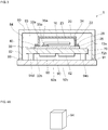
Figs. 1 to 5 . In this case,Fig. 1 is an exploded perspective view of the piezoelectric oscillation device,Fig. 2 is an exploded perspective view of a piezoelectric vibrator that is part of the piezoelectric oscillation device inFig. 1 , andFig. 3 is a sectional view taken along line III-III inFig. 1 .Figs. 4 and5 are diagrams for explaining a substrate holding member of the piezoelectric oscillation device. - As illustrated in
Fig. 1 , apiezoelectric oscillation device 1 according to this embodiment includes apiezoelectric vibrator 50, aheating element 60, anelectronic component 62, asubstrate 70 on which prescribed electrodes (not illustrated) are formed, alid member 80, abase member 90, andsubstrate holding members 94. Thepiezoelectric vibrator 50 is mounted on one main surface of thesubstrate 70 and theheating element 60, which is for heating thepiezoelectric vibrator 50, and theelectronic component 62, which is electrically connected to thepiezoelectric vibrator 50, are mounted on the other main surface of thesubstrate 70. Thesubstrate 70 is attached to thebase member 90 with a prescribed spacing therebetween via thesubstrate holding members 94. Thelid member 80 is attached to thebase member 90 and thepiezoelectric vibrator 50 and thesubstrate 70 are housed inside the thus created space. In other words, thelid member 80 and thebase member 90 serve as a case or package for housing thepiezoelectric vibrator 50, theheating element 60, and theelectronic component 62. Hereafter, the individual constituent elements will be specifically described. - First, the
piezoelectric vibrator 50 will be described. As illustrated inFig. 2 , thepiezoelectric vibrator 50 according to this embodiment includes apiezoelectric vibration element 10, acap 20, which is an example of a lid member, and asubstrate 30, which is an example of a base member. Thecap 20 and thesubstrate 30 form a case or package for housing thepiezoelectric vibration element 10. - The
piezoelectric vibration element 10 includes apiezoelectric piece 11, and first andsecond excitation electrodes piezoelectric piece 11. Thefirst excitation electrode 14a is formed on afirst surface 12a, which is a main surface, of thepiezoelectric piece 11, and thesecond excitation electrode 14b is formed on asecond surface 12b, which is a main surface, of thepiezoelectric piece 11 on the opposite side from thefirst surface 12a of thepiezoelectric piece 11. - The
piezoelectric piece 11 is formed of a certain piezoelectric material. This material is not especially limited. In the example illustrated inFig. 2 , thepiezoelectric piece 11 is an AT-cut crystal piece. In this case, thepiezoelectric vibration element 10 is a crystal vibration element. In addition, thepiezoelectric vibrator 50 is a crystal vibrator. An AT-cut crystal substrate is obtained by performing cutting such that main surfaces of the crystal substrate are surfaces that are parallel to a plane defined by an X axis and a Z' axis (Hereafter, referred to as an "XZ' plane". Similar definitions are used for planes specified using the other axes), where among an X axis, a Y axis, and a Z axis, which are the crystallographic axes of an artificial crystal, a Y' axis and a Z' axis are axes that are respectively obtained by rotating the Y axis and the Z axis 35°15' ± 1°30' around the X axis in a direction from the Y axis toward the Z axis. In the example illustrated inFig. 2 , thepiezoelectric piece 11, which is an AT cut crystal substrate, has long sides that are parallel to the Z' axis, short sides that are parallel to the X axis, and a thickness direction that is parallel to the Y' axis direction, and has a rectangular shape in the XZ' plane. A crystal vibrator, in which an AT-cut crystal substrate is employed, has high frequency stability over a wide temperature range, has excellent degradation with time characteristics, and can be manufactured at a low cost. A thickness shear mode is used as a main vibration in an AT-cut crystal vibrator. - The piezoelectric piece according to this embodiment is not limited to this configuration. For example, an AT-cut crystal substrate having a longitudinal direction that is parallel to the X axis direction and a lateral direction that is parallel to the Z' axis direction may be adopted. Alternatively, a crystal substrate having a cut other than an AT cut (for example, BT cut or the like) may be adopted, or another piezoelectric material other than a crystal such as a ceramic may be adopted.
- The
first excitation electrode 14a is formed on thefirst surface 12a of the piezoelectric piece 11 (XZ' plane on positive Y' axis direction side), and thesecond excitation electrode 14b is formed on thesecond surface 12b (XZ' plane on negative Y' axis direction side) of thepiezoelectric piece 11, which is on the opposite side from thefirst surface 12a of thepiezoelectric piece 11. The first andsecond excitation electrodes piezoelectric piece 11 interposed therebetween in a plan view of the XZ' plane. Theexcitation electrodes excitation electrodes piezoelectric piece 11. - A
connection electrode 16a, which is electrically connected to thefirst excitation electrode 14a via anextension electrode 15a, and aconnection electrode 16b, which is electrically connected to thesecond excitation electrode 14b via anextension electrode 15b, are formed on thepiezoelectric piece 11. Specifically, theextension electrode 15a extends from thefirst excitation electrode 14a toward the short edge on the negative Z' axis direction side on thefirst surface 12a, passes over the side surface of thepiezoelectric piece 11 on the negative Z' axis direction side, and is connected to theconnection electrode 16a, which is formed on thesecond surface 12b. On the other hand, theextension electrode 15b extends from thesecond excitation electrode 14b toward the short edge on the negative Z' axis direction side on thesecond surface 12b, and is connected to theconnection electrode 16b, which is formed on thesecond surface 12b. Theconnection electrodes connection electrodes substrate 30 and are mechanically held on thesubstrate 30 via electricallyconductive holding members connection electrodes extension electrodes - The above-mentioned electrodes including the first and
second excitation electrodes - As illustrated in
Fig. 3 , thecap 20 has arecess 24 that opens so as to face afirst surface 32a of thesubstrate 30. Therecess 24 is provided with aside wall portion 22, which is formed so as to stand upright from a bottom surface of therecess 24, along the entire periphery of the opening. In addition, thecap 20 has a facingsurface 26, which faces thefirst surface 32a of thesubstrate 30, provided along the edge of the opening of therecess 24. Thecap 20 may have aflange portion 28 that protrudes from theside wall portion 22 in a direction from the opening toward the outside, and in this case theflange portion 28 has the facingsurface 26. In this way, the bonding area between thecap 20 and thesubstrate 30 can be increased by bonding theflange portion 28 and thesubstrate 30 to each other. Therefore the strength of the bond between thecap 20 and thesubstrate 30 can be improved. - There are no particular restrictions on the shape of the
cap 20 in this embodiment, and for example thecap 20 may not have theflange portion 28 and a leading end of theside wall portion 22 formed so as to stand substantially vertical from the bottom surface of therecess 24 may instead be bonded to thesubstrate 30. - There are no particular restrictions on the material of the
cap 20, and for example, thecap 20 may be formed of a conductive material such as a metal. With this configuration, a superior electromagnetic shielding function can be added by electrically connecting thecap 20 to the ground potential. Alternatively, thecap 20 may be composed of an insulating material or may have a composite structure composed of a conductive material and an insulating material. - As illustrated in
Fig. 2 , thepiezoelectric vibration element 10 is mounted on thefirst surface 32a (upper surface) of thesubstrate 30. In the example illustrated inFig. 2 , thesubstrate 30 has a longitudinal direction that is parallel to the Z' axis direction, a lateral direction that is parallel to the X axis direction, and a thickness direction that is parallel to the Y' axis direction, and has a rectangular shape in the XZ' plane. Thesubstrate 30 may be formed of an insulating ceramic, for example. Alternatively, thesubstrate 30 may be formed of a glass material, a crystal material, a glass epoxy resin, or the like. Thesubstrate 30 may be formed of a single layer or a plurality of layers, and in the case where thesubstrate 30 is formed of a plurality of layers, an insulating layer may be included that is formed as the outermost layer at thefirst surface 32a. In addition, thesubstrate 30 may be shaped like a flat plate or may have a recessed shape that opens so as to face thecap 20. As illustrated inFig. 3 , thepiezoelectric vibration element 10 is hermetically sealed inside an inner space (cavity) 23 that is surrounded by therecess 24 of thecap 20 and thesubstrate 30 by bonding thecap 20 and thesubstrate 30 to each other via abonding material 40. - The
bonding material 40 is provided along the entire periphery of thecap 20 or thesubstrate 30, and is interposed between the facingsurface 26 of theside wall portion 22 of thecap 20 and thefirst surface 32a of thesubstrate 30. Thebonding material 40 may be composed of an insulating material. The insulating material may be a glass material (for example, a low-melting-point glass) or a resin material (for example, an epoxy-based resin), for example. As a result of using such an insulating material, compared with metal bonding, the heating temperature can be suppressed and the manufacturing facility can be simplified. In the case where an electromagnetic shielding function of thecap 20 is to be improved, it is preferable that thecap 20 be bonded to thesubstrate 30 via thebonding material 40 while securing an electrical connection to thecap 20. - In the example illustrated in
Fig. 3 , one end of the piezoelectric vibration element 10 (end portion on electricallyconductive holding members piezoelectric vibration element 10 is a free end. As a modification, thepiezoelectric vibration element 10 may be fixed to thesubstrate 30 at both ends thereof in the longitudinal direction. - As illustrated in
Fig. 2 , thesubstrate 30 includesconnection electrodes first surface 32a, andextension electrodes connection electrodes first surface 32a. Theextension electrodes substrate 30 such that thepiezoelectric vibration element 10 can be arranged substantially in the center of thefirst surface 32a of thesubstrate 30. - The
connection electrode 16a of thepiezoelectric vibration element 10 is connected to theconnection electrode 33a via the electrically conductive holdingmember 36a, and theconnection electrode 16b of thepiezoelectric vibration element 10 is connected to theconnection electrode 33b via the electrically conductive holdingmember 36b. - The
extension electrode 34a extends from theconnection electrode 33a toward any one corner of thesubstrate 30, and theextension electrode 34b extends from theconnection electrode 33b toward another one corner of thesubstrate 30. In addition, a plurality ofouter electrodes substrate 30, and in the example illustrated inFig. 2 , theextension electrode 34a is connected to theouter electrode 35a formed in the corner that is on the negative X axis direction side and negative Z' axis direction side, and theextension electrode 34b is connected to theouter electrode 35b formed in the corner on the positive X axis direction side and the positive Z' axis direction side. In addition, as illustrated inFig. 2 , theouter electrodes piezoelectric vibration element 10. In addition, these outer electrodes may be dummy electrodes that are not electrically connected to an electronic component mounted on thesubstrate 30. As a result of such dummy electrodes being formed, the process of applying a conductive material for forming the outer electrodes is simplified and outer electrodes can be formed in all the corners, and therefore the processing step of bonding the piezoelectric vibrator to another member is also simplified. In addition, ground electrodes to which a ground potential is supplied may be formed instead of theouter electrodes cap 20 is composed of an electrically conductive material, a superior electromagnetic shielding function may be added to thecap 20 by connecting thecap 20 to theouter electrodes - In the example illustrated in
Fig. 2 , the corners of thesubstrate 30 each have a cut-away side surface formed by cutting away part of the corner to form a cylindrical curved surface shape (also referred to as castellation shape), and theouter electrodes 35a to 35d are formed in a continuous manner on these cut-away side surfaces and asecond surface 32b of thesubstrate 30. The shape of the corners of thesubstrate 30 is not limited to this example, and the cut-away shape may be a flat surface shape or the corners may not be cut away and the four corners may instead have a right-angle rectangular shapes in plan view. - The configurations of the connection electrodes, the extension electrodes, and outer electrodes of the
substrate 30 are not limited to the above-described examples, and can be modified in various ways. For example, theconnection electrodes first surface 32a of thesubstrate 30 such as one connection electrode being formed on the positive Z' axis direction side and the other connection electrode being formed on the negative Z' axis direction side. In this configuration, thepiezoelectric vibration element 10 is supported on thesubstrate 30 at both one end and the other end thereof in the longitudinal direction. In addition, the number of outer electrodes is not limited to four, and a similar effect is obtained even if there are only two outer electrodes arranged at diagonally opposite corners. Furthermore, the outer electrodes are not limited to being arranged in the corners, and one or more outer electrodes may instead be formed on any parts of the side surfaces of thesubstrate 30 excluding the corners. In this case, as has already been described, cut-away side surfaces may be formed by cutting away parts of the side surfaces to form cylindrical curved surface shapes, and the outer electrodes may be formed on these parts of the side surfaces excluding the corners. In addition, theother electrodes first surface 32a to thesecond surface 32b may be formed in thesubstrate 30, and electrical connections from connection electrodes formed on thefirst surface 32a to thesecond surface 32b may be realized using the through holes. - In the
piezoelectric vibrator 50 illustrated inFig. 2 , an alternating-current voltage is applied between the pair of first andsecond excitation electrodes piezoelectric vibration element 10 via theouter electrodes substrate 30, and as a result thepiezoelectric substrate 11 vibrates in a prescribed vibration mode such as a thickness shear vibration mode, and resonance characteristics are obtained together with the vibration. - Returning to
Fig. 1 , the other constituent elements of thepiezoelectric oscillation device 1 will be described. - In the example illustrated in
Fig. 1 , thepiezoelectric vibrator 50 is mounted on afirst surface 72a, which is a main surface, of thesubstrate 70, and theheating element 60 and theelectronic component 62 are mounted on asecond surface 72b, which is a main surface, of thesubstrate 70 on the opposite side from thefirst surface 72a. Prescribed electrodes, which are not illustrated, are formed on thesubstrate 70, and thepiezoelectric vibrator 50, theheating element 60, and theelectronic component 62 are respectively electrically connected to wiring lines of the electrodes. Furthermore, thepiezoelectric vibration element 10 may be mounted on thefirst surface 72a, which is a main surface of thesubstrate 70, without using thesubstrate 30. In this case, theconnection electrode 16a of thepiezoelectric vibration element 10 is connected to aconnection electrode 33a provided on thesubstrate 70 via the electrically conductive holdingmember 36a, and theconnection electrode 16b of thepiezoelectric vibration element 10 is connected to aconnection electrode 33b provided on thesubstrate 70 via the electrically conductive holdingmember 36b. - The
heating element 60 may be arranged close to thepiezoelectric vibrator 50 in order to improve the effect of supplying heat to thepiezoelectric vibrator 50. For example, as illustrated inFig. 1 , theheating element 60 may be provided in a region of thesecond surface 72b that at least partially overlaps thepiezoelectric vibrator 50, thesecond surface 72b being the surface of thesubstrate 70 on the opposite side from the upper surface of thepiezoelectric vibrator 50. Alternatively, as a modification, theheating element 60 may be provided close to thepiezoelectric vibrator 50 on thefirst surface 72a of thesubstrate 70, which is the side of thesubstrate 70 on which thepiezoelectric vibrator 50 is mounted. - The
electronic component 62 is electrically connected to thepiezoelectric vibration element 10 and forms an oscillation circuit that is for generating a reference signal such as a clock signal. Theelectronic component 62 is electrically connected to thepiezoelectric vibrator 50 via electrodes (not illustrated) that are formed on thesubstrate 70, and is configured so as to be able to be electrically connected to a component outside the piezoelectric oscillation device 1 (for example, a circuit board) via electrodes (not illustrated) that are formed on thebase member 90. Theelectronic component 62 is an integrated circuit element, for example. Other than an oscillation circuit, the integrated circuit element may include prescribed circuits that are necessary in order for thepiezoelectric vibrator 50 to perform prescribed operations. For example, the integrated circuit element may include an oscillation circuit for generating a reference signal such as a clock signal, a temperature sensor circuit that detects the temperature of thepiezoelectric vibration element 10, and a control circuit that controls the temperature sensor circuit. Although theheating element 60 is a separate constituent element from theelectronic component 62 in the example illustrated inFig. 1 , as a modification, an integrated circuit element, which is an example of theelectronic component 62, may further include a control circuit that controls the heating element and may further include the heating element. - One or more other electronic components (may be active elements or passive elements) may be mounted on the
substrate 70. In addition, various circuits built into the integrated circuit element may instead be formed as separate electronic components, and these electronic components may be mounted on thefirst surface 72a and/or thesecond surface 72b of thesubstrate 70. - The material of the
substrate 70 is not particularly limited, and thesubstrate 70 may be formed of an insulating ceramic, for example. Alternatively, thesubstrate 70 may be formed of a glass material, a crystal material, a glass epoxy resin, or the like. - As illustrated in
Fig. 3 , thelid member 80 is a cap and has arecess 84 that opens so as to face afirst surface 72a of thesubstrate 70. Therecess 84 is provided with aside wall portion 82, which is formed so as to stand upright from a bottom surface of therecess 84, along the entire periphery of the opening. In addition, the cap, which is thelid member 80, has a facingsurface 86, which faces thefirst surface 72a of thesubstrate 70, provided along the edge of the opening of therecess 84. In the example illustrated inFig. 3 , a leading end of theside wall portion 82 formed so as to stand substantially vertical from the bottom surface of therecess 84 is bonded to thesubstrate 70. Alternatively, as a modification, the lid member may have a flange portion similarly to thecap 20 of thepiezoelectric vibrator 50. - There are no particular restrictions on the material of the
lid member 80, and for example, thelid member 80 may be formed of a conductive material such as a metal. With this configuration, a superior electromagnetic shielding function can be added by electrically connecting thelid member 80 to the ground potential. Alternatively, thelid member 80 may be composed of an insulating material or may have a composite structure composed of a conductive material and an insulating material. - In addition, the shape of the
lid member 80 is not limited to that of the above-described cap, and provided that thelid member 80 has a configuration that allows thepiezoelectric vibrator 50 to be housed thereinside when combined with thebase member 90, the shape of thelid member 80 is not restricted. For example, in the case where thepiezoelectric vibration element 10 is mounted on thefirst surface 72a of thesubstrate 70, thecap 20 may be bonded to thefirst surface 72a of thesubstrate 70 and thelid member 80 may be bonded to thebase member 90 such that thepiezoelectric vibration element 10 is housed inside therecess 24 of thecap 20. - The
substrate 70 is held on afirst surface 92a of thebase member 90, which is a main surface of thebase member 90. Specifically, one or more substrate holding members 94 (foursubstrate holding members Fig. 1 ) are provided on thefirst surface 92a of thebase member 90 and thesesubstrate holding members 94 support thesecond surface 72b of thesubstrate 70, and in this way, thesubstrate 70 is held at a prescribed spacing from thebase member 90. Electrodes (not illustrated), which are for realizing electrical connections to outside thepiezoelectric oscillation device 1, are formed on thebase member 90. Electrodes for realizing electrical connections to the outside such as to a circuit board, which is not illustrated, may be formed on asecond surface 92b of thebase member 90, which is on the opposite side from thefirst surface 92a of thebase member 90. - The material of the
base member 90 is not particularly limited, and thebase member 90 may be formed of an insulating ceramic, for example. Alternatively, thebase member 90 may be formed of a glass material, a crystal material, a glass epoxy resin, or the like. The shape of thebase member 90 is also not particularly limited, and for example, thebase member 90 may have a flat plate shape, as illustrated inFig. 1 , or may have a recessed shape that opens so as to face thelid member 80. - As illustrated in
Fig. 3 , thelid member 80 and thebase member 90 are bonded to each other via abonding material 91, and as a result thepiezoelectric vibrator 50, theheating element 60, and theelectronic component 62 are hermetically sealed in an inner space (cavity) 83 that is surrounded by therecess 84 of thelid member 80 and thebase member 90. In addition, a suitable material can be chosen for thebonding material 91 in line with the materials of thelid member 80 and thebase member 90, and for example, the content described in relation to thebonding material 40 of thepiezoelectric vibrator 50 can be applied. - Next, a substrate holding member according to this embodiment will be further described while referring to
Fig. 1 ,Figs. 4A to 4F , andFig. 5 . - The
substrate holding member 94 includes a conductive part. The conductive part is electrically connected to at least one out of thepiezoelectric vibrator 50, theheating element 60, and theelectronic component 62 mounted on thesubstrate 70, and is for electrically connecting any of these elements to the outside. In this embodiment, the conductive part of thesubstrate holding member 94 has a lower thermal conductivity than metal. Therefore, the amount of heat, out of the heat generated by theheating element 60, that is radiated to the outside via thesubstrate holding member 94 can be suppressed, thepiezoelectric vibration element 10 can be efficiently heated, and power consumption can be reduced. - The conductive part of the
substrate holding member 94 is composed of an epoxy-based conductive resin material, for example. The epoxy-based conductive resin material is a composite material in which a conductive filler such as silver is contained in an epoxy-based resin serving as a binder, and the entirety of this composite material functions as the conductive part. The thermal conductivity of the epoxy-based conductive resin material is 5.0 W/(m-K). This value is lower than the thermal conductivity of a single metal (for example, the thermal conductivity of copper is 400 W/(m-K)) or an alloy (for example, the thermal conductivity of nickel silver is 40 W/(m-K)). The conductive part of thesubstrate holding member 94 is not limited to being composed of an epoxy-based conductive resin material and may be composed of another type of conductive resin material. - In the example illustrated in
Fig. 1 , the entirety of eachsubstrate holding member 94 is formed of the conductive part. Alternatively, not limited to this example, part of eachsubstrate holding member 94 may be formed of the conductive part, as described later. - As illustrated in
Fig. 1 , thesubstrate holding members 94 may be columnar bodies. In this case, the conductive part is exposed at both the side of the columnar body that faces thesubstrate 70 and the side of the columnar body that faces thebase member 90. In addition, the columnar body may have flat side surfaces or a curved side surface. As illustrated inFig. 1 , the height of thesubstrate holding members 94 in the Y' direction (for example, average height) is larger than the width of thesubstrate holding members 94 in the XZ' plane (for example, average width). In the case where thesubstrate holding members 94 have a circular shape in the XZ' plane, the height of thesubstrate holding members 94 in the Y' direction (for example, average height) is larger than the diameter of thesubstrate holding members 94 in the XZ' plane (for example, average diameter). Thus, provided that thesubstrate holding members 94 having a long thin shape in which the cross-sectional width in the XZ' plane is smaller than the height in the Y' direction, the amount of heat transmitted via thesubstrate holding members 94 can be reduced. In addition, the "diameter of a substrate holding member" may be the diameter of a circumscribing circle of the substrate holding member in a plane contacting the XZ' plane. - The substrate holding members may have any of various shapes. For example, as illustrated in
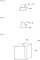
Fig. 4A , thesubstrate holding members 94 may have a prism-like shape in which the side surfaces of the columnar body be flat. The cross-sectional shape of the prism-like shape may be a polygon such as a rectangle. - Alternatively, as illustrated in
Fig. 4B , asubstrate holding member 95 may be adopted that has a square truncated pyramid shape as one example of a truncated pyramid shape. In this case, the shape may be a shape in which the cross-sectional width becomes smaller toward thesubstrate 70 and specifically the shape may be a tapered shape. In other words, the side surfaces of thesubstrate holding member 95 may be tapered surfaces. Alternatively, as illustrated inFig. 4C , asubstrate holding member 96 having a cylindrical shape may be adopted. Alternatively, as illustrated inFig. 4D , asubstrate holding member 97 having a truncated cone shape may be adopted. Alternatively, a substrate holding member may be formed by combining a plurality of three-dimensional shapes, as illustrated inFigs. 4E and 4F . For example, as illustrated inFig. 4E , asubstrate holding member 98 may be adopted that includes afirst part 98a having a prism-like shape and asecond part 98b having a prism-like shape and having a larger cross-sectional width than thefirst part 98a. In this case, the part having the larger cross-sectional width may be arranged on thebase member 90 side. In addition, as illustrated inFig. 4F , asubstrate holding member 99 may be adopted that includes a square-column-shapedfirst part 99a and a square-column-shapedsecond part 99b that has a larger cross-sectional width than thefirst part 99a, and in which opposite side surfaces of the first andsecond parts - In the case where the substrate holding member has a shape in which the cross-sectional width varies in the height direction, provided that the shape is a shape in which the cross-sectional width becomes smaller toward the
substrate 70, which is the side on which theheating element 60 is provided, the amount of heat that is transmitted from theheating element 60 to thebase member 90 via thesubstrate 70 can be made small. Therefore, the efficiency with which thepiezoelectric vibration element 10 is heated is improved. Alternatively, the cross-sectional width of the substrate holding member may become smaller toward thebase member 90 on the opposite side, or the substrate holding member may have a shape in which the cross-sectional width is smaller in the center than at the ends in the height direction. Since the amount of heat that is transmitted through the substrate holding member and radiated to the outside depends on the size of the cross-sectional width of the substrate holding member (in other words, the cross-sectional area), it is possible to reduce the amount of heat that is radiated to the outside due to the presence of a part having a relatively small cross-sectional width. - Although examples are illustrated in
Figs. 1 and4 in which the entirety of the substrate holding member is formed of a conductive part, as a modification, asubstrate holding member 194 may have aconductive part 196 and acovering part 198 that covers theconductive part 196, as illustrated inFig. 5 . In this case, theconductive part 196 is exposed from the coveringpart 198 on the side facing thesubstrate 70 and the side facing thebase member 90. In addition, the coveringpart 198 has a lower thermal conductivity than theconductive part 196. The coveringpart 198 may be formed of an insulating resin material or may be formed of an organic or inorganic composite material. Examples of a material constituting the coveringpart 198 include an epoxy resin, an acrylic resin, and a glass epoxy material. The content described for the case where the entirety of the substrate holding member is formed of the conductive part applies to the rest of the configuration. According to the configuration illustrated inFig. 5 , the amount of heat radiated to the outside via thesubstrate holding member 194 can be further suppressed compared with the case where the entirety of thesubstrate holding member 194 is formed of the conductive part. - Next, a method of manufacturing the piezoelectric oscillation device according to this embodiment will be described while referring to
Figs. 6 to 9 . In this case,Fig. 6 is a flowchart illustrating a method of manufacturing the piezoelectric oscillation device according to this embodiment. Furthermore,Figs. 7A to 7F are diagrams illustrating an example of a method of forming a substrate holding member according to this embodiment, andFigs. 8 and9 are diagrams illustrating a modification of the method of forming a substrate holding member according to this embodiment. - As illustrated in
Fig. 6 , thepiezoelectric vibrator 50, theheating element 60, and theelectronic component 62 are prepared and then mounted on the substrate 70 (S10). Next, thesubstrate holding members 94 are formed (S12). After that, thesubstrate 70 is attached to thebase member 90 with a prescribed spacing therebetween via the substrate holding members 94 (S14). Finally, thelid member 80 is attached to the base member 90 (S16). In this way, thepiezoelectric oscillation device 1 can be obtained in which thepiezoelectric vibrator 50, theheating element 60, and theelectronic component 62 are housed in a package formed of thelid member 80 and thebase member 90. - The
substrate holding members 94 can be formed using various manufacturing methods. For example, as illustrated inFigs. 7A to 7F , a plurality ofsubstrate holding members 94 may be formed on asheet 100 by forming aconductive resin block 102 on thesheet 100 and then shaping and dividing theconductive resin block 102 to form the individualsubstrate holding members 94. - Specifically, first, as illustrated in
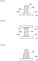
Fig. 7A , theconductive resin block 102 is formed by applying a conductive resin material in the form of a paste to thesheet 100, which has adhesiveness, and then curing the material using heat or the like. Next, as illustrated inFigs. 7B and 7C , aconductive resin block 104 is obtained by subjecting the top surface and the side surfaces of the curedconductive resin block 102 to removal machining using a dicing blade (not illustrated) in order to shape theconductive resin block 102. After that, as illustrated inFigs. 7D and7E , a plurality ofsubstrate holding members 94 having a prescribed shape are obtained by cutting theconductive resin block 104 on thesheet 100 using a dicing blade in order to divide theconductive resin block 104 into the individualsubstrate holding members 94. Then, the plurality ofsubstrate holding members 94 are peeled off thesheet 100. For example, thesheet 100 may have a property in which the adhesiveness thereof falls when subjected to heat or the like, and in such a case, the plurality ofsubstrate holding members 94 can be easily removed from thesheet 100 by heating thesheet 100. Finally, as illustrated inFig. 7F , thesubstrate holding member 94 is arranged between thesecond surface 72b of thesubstrate 70 and thefirst surface 92a of thebase member 90 and thesubstrate 70 is held on thebase member 90 via thesubstrate holding member 94. In this case, for example,conductive material 73 may be provided on thesecond surface 72b of thesubstrate 70 andconductive material 93 may be provided on thefirst surface 92a of thebase member 90, and theconductive materials substrate holding member 94. Theconductive materials substrate holding member 94 where the electrical connection is to be realized may be subjected to a plating treatment in advance. - According to the manufacturing method illustrated in
Figs. 7A to 7F , a plurality ofsubstrate holding members 94 can be efficiently manufactured using comparatively few steps. In addition, shaping processing using a dicing blade can be performed on thesheet 100, and therefore there is a high degree of freedom in the shaping processing and the shaping processing itself is simple. - As a modification, as illustrated in
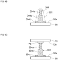
Figs. 8A to 8C , thesubstrate holding member 94 may be formed directly on thebase member 90. Specifically, first, as illustrated inFig. 8A , aconductive resin block 292 is formed by applying a conductive resin material in the form of a paste to thefirst surface 92a of thebase member 90 and then curing the material using heat or the like. Next, as illustrated inFig. 8B , the curedconductive resin block 292 is shaped by subjecting the top surface and the side surfaces of theconductive resin block 292 to removal machining, and asubstrate holding member 294 of a prescribed shape is thus obtained. In this example, thesubstrate holding member 294 includes afirst part 294a and asecond part 294b, which has a larger cross-sectional width than thefirst part 294a. Thesubstrate holding member 294 may be formed in a prism-like shape in which the side surfaces of a columnar body are configured so as be flat. In addition, as has already been described, the substrate holding member may be formed in a cylindrical shape or a truncated cone shape configured such that a side surface of a columnar body of the substrate holding member is curved, and in this case, since the side surface of the columnar body is already configured to be curved as a result of the conductive resin material in the form of a paste being cured using heat or like as illustrated inFig. 8A , it is sufficient to perform shaping in which only the top surface of theconductive resin block 292 is cut inFig. 8B . Corner portions of the substrate holding member may be subjected to chamfering. - As another further modification, as illustrated in
Figs. 9A to 9C , on thebase member 90, asubstrate holding member 394 may be formed that includes afirst part 394a, asecond part 394b having a larger cross-sectional width than thefirst part 394a, and athird part 394c that has a larger cross-sectional width than thesecond part 394b. This shape can be obtained by shaping aconductive resin block 392 formed on thefirst surface 92a of thebase member 90 using a dicing blade. - According to the manufacturing method illustrated in
Figs. 8 and9 , the substrate holding member can be formed directly on thebase member 90, and therefore thepiezoelectric oscillation device 1 can be manufacturing using a small number of steps. - Assuming a uniform material having a temperature difference ΔT between a high-temperature portion T1 and a low-temperature portion T2, the amount of heat that is transferred can be approximated by
formula 1 below. In this case, the smaller the cross-sectional area of a column (average cross-sectional diameter) or the larger the length of the column, the smaller the amount of heat that is transferred by thermal conduction. An aspect ratio γ of the substrate holding member is given by H/D, where D is the average cross-sectional width of the substrate holding member (for example, average diameter) and H is the average height of the substrate holding member. When the substrate holding member has a solid structure, the amount of heat that is transferred can be made small by making the aspect ratio γ high. As a result, a high thermal insulation effect is obtained. From the viewpoint of the thermal insulation effect, the value of the aspect ratio γ is preferably greater than or equal to 2. On the other hand, when the substrate holding member is formed so as to have a long thin structure in order to make the aspect ratio γ high, the mechanical strength of the substrate holding member becomes lower. From the viewpoint of maintaining the mechanical strength of thesubstrate holding member 94, the value of the aspect ratio γ is preferably less than or equal to 5 and the value of the aspect ratio γ is further preferably less than or equal to 4.
- In addition, toppling over of the substrate holding member occurring when the substrate holding member is subjected to a removal machining process and an assembly process can be reduced by performing machining such that a cross-sectional dimension of a bottom part of the substrate holding member is given a large step shape. Thus, a removal machining process and an assembly process can be easily implemented. In particular, when a separately formed substrate holding member is arranged on the
base member 90 rather than a substrate holding member being directly formed on and bonded to a surface of thebase member 90, the substrate holding member can be prevented from toppling over when assembly is performed and the arrangement process and the machining process are simplified. In addition, in the case where the substrate holding member is formed together with thebase member 90, the substrate holding member generated by machining stress when the substrate holding member is subjected to cutting machining can be prevented. - Although a mode in which a conductive resin block is subjected to shaping processing has been described above, the present invention is not limited to this mode, and a substrate holding member having a prescribed shape can instead be formed by for example pouring a conductive resin material in the form of a paste into a molding member having a prescribed shape and curing the material using heat or the like or chemically curing the material. According to this mode, the amount of material used can be reduced and the substrate holding member can be easily formed.
- With the method of manufacturing a piezoelectric oscillation device according to this embodiment, as has already been described, a piezoelectric oscillation device can be manufactured that can efficiently heat the
piezoelectric vibration element 10 and can reduce power consumption. - As described above, with the piezoelectric oscillation device and manufacturing method therefor according to embodiments of the present invention, the following operational effects can be realized by adopting any of the configurations described above.
- According to a configuration described above, a substrate on which a heating element is provided is held on a base member via a substrate holding member that includes a conductive part having a lower thermal conductivity than a metal such as copper or aluminum, and therefore the amount of heat, out of heat generated by the heating element, that radiates to the outside via the substrate holding member can be suppressed.
- According to a configuration described above, the conductive part is composed of a conductive resin material (epoxy-based conductive resin material), and therefore a substrate holding member that includes a conductive part having a low thermal conductivity can be obtained with a simple configuration. The thermal conductivity may be measured using a steady heat flow measurement method.
- According to a configuration described above, the substrate holding member is a columnar body, and therefore the substrate can be stably held on the base member. In addition, since the substrate holding member is a columnar body, adjusting the height and cross-sectional width of the substrate holding member is a simple matter. Therefore, the amount of heat radiated to the outside via the substrate holding member can be easily adjusted. In particular, the amount of heat radiated to the outside via the substrate holding member can be further reduced by making the height of the substrate holding member larger than the cross-sectional width of the substrate holding member.
- The purpose of the embodiments described above is to enable easy understanding of the present invention and the embodiments are not to be interpreted as limiting the present invention. The present invention can be modified or improved without departing from the gist of the invention and equivalents to the present invention are also included in the present invention. In other words, appropriate design changes made to the embodiments by one skilled in the art are included in the scope of the present invention so long as the changes have the characteristics of the present invention. For example, the elements included in the embodiments and the arrangements, materials, conditions, shapes, dimensions, and so forth of the elements are not limited to those exemplified in the embodiments and can be appropriately changed. In addition, the elements included in the embodiments can be combined as much as technically possible and such combined elements are also included in the scope of the present invention so long as the combined elements have the characteristics of the present invention. Reference Signs List
-
- 1
- piezoelectric oscillation device
- 10
- piezoelectric vibration element
- 50
- piezoelectric vibrator
- 60
- heating element
- 62
- electronic component
- 70
- substrate
- 80
- lid member
- 90
- base member
- 94
- substrate holding member
Claims (18)
- A piezoelectric oscillation device comprising:a piezoelectric vibrator including a piezoelectric vibration element;a heating element that heats the piezoelectric vibration element;an electronic component that is electrically connected to the piezoelectric vibration element;a substrate on which the piezoelectric vibrator, the heating element and the electronic component are mounted; anda base member to which the substrate is attached with a prescribed spacing therebetween via a substrate holding member;wherein the substrate holding member has a conductive part and the conductive part has a lower thermal conductivity than metal.
- The piezoelectric oscillation device according to Claim 1, wherein the conductive part is composed of a conductive resin material.
- The piezoelectric oscillation device according to Claim 2, wherein the conductive resin material includes an epoxy-based conductive resin material.
- The piezoelectric oscillation device according to any one of Claims 1 to 3, wherein the substrate holding member is entirely formed of the conductive part.
- The piezoelectric oscillation device according to any one of Claims 1 to 4, wherein the substrate holding member has a covering part that covers the conductive part.
- The piezoelectric oscillation device according to Claim 5, wherein the covering part has a lower thermal conductivity than the conductive part.
- The piezoelectric oscillation device according to any one of Claims 1 to 6, wherein the substrate holding member is a columnar body.
- The piezoelectric oscillation device according to Claim 1, wherein the electronic component is electrically connected to the piezoelectric vibration element and is an integrated circuit element that includes an oscillation circuit that generates a reference signal that is a clock signal.
- The piezoelectric oscillation device according to Claim 7, wherein a ratio of an average height of the columnar body with respect to an average cross-sectional width of the columnar body is greater than or equal to 2.
- The piezoelectric oscillation device according to Claim 9, wherein the ratio of the average height of the columnar body with respect to the average cross-sectional width of the columnar body is less than or equal to 5.
- The piezoelectric oscillation device according to Claim 9, wherein the ratio of the average height of the columnar body with respect to the average cross-sectional width of the columnar body is less than or equal to 4.
- The piezoelectric oscillation device according to any one of Claims 1 to 11, further comprising:
a lid member that is attached to the base member such that the piezoelectric vibrator and the substrate are housed thereinside. - A method of manufacturing a piezoelectric oscillation device, the method comprising:(a) mounting, on a substrate, a piezoelectric vibrator that includes a piezoelectric vibration element, a heating element that heats the piezoelectric vibration element, and an electronic component that is electrically connected to the piezoelectric vibration element;(b) forming a substrate holding member that is for holding the substrate on the base member; and(c) attaching the substrate to the base member with a prescribed spacing therebetween via the substrate holding member;wherein the substrate holding member includes a conductive part, and in (b), the conductive part is formed of a material having a lower thermal conductivity than metal.
- The piezoelectric oscillation device according to Claim 13, wherein the conductive part is composed of a conductive resin material.
- The method of manufacturing a piezoelectric oscillation device according to Claim 14, wherein (b) includes forming a conductive resin block by applying a conductive resin material in the form of a paste to a sheet and curing the conductive resin material,
shaping the conductive resin block on the sheet,
obtaining a plurality of the substrate holding members by dividing the conductive resin block on the sheet into individual substrate holding members, and
removing each substrate holding member from the sheet. - The method of manufacturing a piezoelectric oscillation device according to Claim 14, wherein (b) includes forming a conductive resin block by applying a conductive resin material in the form of a paste to the base member and curing the conductive resin material, and
shaping the conductive resin block on the base member. - The method of manufacturing a piezoelectric oscillation device according to Claim 14, wherein (b) includes pouring the conductive resin material in the form of a paste into a molding member and curing the conductive resin material.
- The method of manufacturing a piezoelectric oscillation device according to Claim 13, wherein the electronic component is electrically connected to the piezoelectric vibration element and is an integrated circuit element that includes an oscillation circuit that generates a reference signal that is a clock signal.
Applications Claiming Priority (2)
| Application Number | Priority Date | Filing Date | Title |
|---|---|---|---|
| JP2015252121 | 2015-12-24 | ||
| PCT/JP2016/088384 WO2017111020A1 (en) | 2015-12-24 | 2016-12-22 | Pieozoelectric oscillation device and method for manufacturing same |
Publications (2)
| Publication Number | Publication Date |
|---|---|
| EP3379723A1 true EP3379723A1 (en) | 2018-09-26 |
| EP3379723A4 EP3379723A4 (en) | 2019-08-07 |
Family
ID=59090456
Family Applications (1)
| Application Number | Title | Priority Date | Filing Date |
|---|---|---|---|
| EP16878907.1A Pending EP3379723A4 (en) | 2015-12-24 | 2016-12-22 | PIEZOELECTRIC OSCILLATION DEVICE AND METHOD FOR MANUFACTURING THE SAME |
Country Status (5)
| Country | Link |
|---|---|
| US (1) | US10707810B2 (en) |
| EP (1) | EP3379723A4 (en) |
| JP (1) | JP6369707B2 (en) |
| CN (1) | CN108432126A (en) |
| WO (1) | WO2017111020A1 (en) |
Families Citing this family (16)
| Publication number | Priority date | Publication date | Assignee | Title |
|---|---|---|---|---|
| JP6662057B2 (en) * | 2016-01-22 | 2020-03-11 | 株式会社大真空 | Piezoelectric oscillator |
| US20180131324A1 (en) * | 2016-08-15 | 2018-05-10 | Bliley Technologies, Inc. | High-Efficiency Ovenized Oscillator |
| JP6956093B2 (en) * | 2016-08-31 | 2021-10-27 | 株式会社村田製作所 | Piezoelectric oscillator |
| CN109804560B (en) * | 2016-10-11 | 2023-03-14 | 株式会社村田制作所 | Piezoelectric resonator and method for manufacturing same |
| CN109743056B (en) * | 2019-02-26 | 2024-06-11 | 泰斗微电子科技有限公司 | Satellite time service device |
| US11929709B2 (en) * | 2020-03-30 | 2024-03-12 | Daishinku Corporation | Oven-controlled crystal oscillator |
| JP7516959B2 (en) * | 2020-07-30 | 2024-07-17 | セイコーエプソン株式会社 | Oscillator |
| JP7593001B2 (en) * | 2020-07-30 | 2024-12-03 | セイコーエプソン株式会社 | Oscillator |
| JP7508936B2 (en) * | 2020-08-06 | 2024-07-02 | セイコーエプソン株式会社 | Oscillator |
| JP7608750B2 (en) * | 2020-08-24 | 2025-01-07 | セイコーエプソン株式会社 | Oscillator |
| JP7543772B2 (en) * | 2020-08-24 | 2024-09-03 | セイコーエプソン株式会社 | Oscillator |
| JP7505564B2 (en) * | 2020-09-07 | 2024-06-25 | 株式会社大真空 | Thermostatic oven type piezoelectric oscillator |
| US12249955B2 (en) * | 2021-02-25 | 2025-03-11 | Daishinku Corporation | Oven-controlled crystal oscillator |
| CN115242209A (en) * | 2021-04-23 | 2022-10-25 | 华为技术有限公司 | Resonator package and oscillator |
| JP7750042B2 (en) * | 2021-11-09 | 2025-10-07 | 株式会社大真空 | Oven-type piezoelectric oscillator |
| JP7803164B2 (en) * | 2022-02-22 | 2026-01-21 | セイコーエプソン株式会社 | Oscillator |
Family Cites Families (17)
| Publication number | Priority date | Publication date | Assignee | Title |
|---|---|---|---|---|
| US6236145B1 (en) * | 2000-02-29 | 2001-05-22 | Cts Corporation | High thermal resistivity crystal resonator support structure and oscillator package |
| JP4855087B2 (en) * | 2005-03-28 | 2012-01-18 | 日本電波工業株式会社 | Constant temperature crystal oscillator |
| JP2007214739A (en) * | 2006-02-08 | 2007-08-23 | Epson Toyocom Corp | Piezoelectric oscillator and electronic equipment |
| JP2007266828A (en) * | 2006-03-28 | 2007-10-11 | Kyocera Kinseki Corp | Piezoelectric device |
| US20090051447A1 (en) * | 2007-08-24 | 2009-02-26 | Mccracken Jeffrey A | Ovenized oscillator |
| CN101946403B (en) * | 2008-02-16 | 2014-12-10 | 精工电子水晶科技股份有限公司 | Piezoelectric vibrator, manufacturing method of piezoelectric vibrator, oscillator, electronic device, and radio wave clock |
| JP2010183227A (en) * | 2009-02-04 | 2010-08-19 | Epson Toyocom Corp | Constant-temperature piezoelectric oscillator |
| JP5747574B2 (en) * | 2011-03-11 | 2015-07-15 | セイコーエプソン株式会社 | Piezoelectric device and electronic equipment |
| JP6123979B2 (en) * | 2012-05-23 | 2017-05-10 | セイコーエプソン株式会社 | Oscillator and electronic device |
| JP5984526B2 (en) | 2012-06-20 | 2016-09-06 | 日本電波工業株式会社 | Surface mount device |
| JP5998872B2 (en) * | 2012-11-26 | 2016-09-28 | セイコーエプソン株式会社 | Piezoelectric oscillator |
| JP2014197730A (en) * | 2013-03-29 | 2014-10-16 | セイコーエプソン株式会社 | Oscillation device, electronic apparatus and mobile object |
| JP6286884B2 (en) | 2013-06-13 | 2018-03-07 | セイコーエプソン株式会社 | Electronic devices, electronic devices, and moving objects |
| JP2015080082A (en) | 2013-10-17 | 2015-04-23 | 京セラクリスタルデバイス株式会社 | Piezoelectric oscillator with temperature chamber |
| JP2015122607A (en) * | 2013-12-24 | 2015-07-02 | セイコーエプソン株式会社 | Oscillator, electronic apparatus, and moving body |
| JP6307869B2 (en) * | 2013-12-24 | 2018-04-11 | セイコーエプソン株式会社 | Electronic components, crystal oscillators with thermostatic chambers, electronic devices, and moving objects |
| JP2015186251A (en) * | 2014-03-26 | 2015-10-22 | 日本電波工業株式会社 | crystal oscillator |
-
2016
- 2016-12-22 JP JP2017558265A patent/JP6369707B2/en not_active Expired - Fee Related
- 2016-12-22 CN CN201680074498.3A patent/CN108432126A/en active Pending
- 2016-12-22 EP EP16878907.1A patent/EP3379723A4/en active Pending
- 2016-12-22 WO PCT/JP2016/088384 patent/WO2017111020A1/en not_active Ceased
-
2018
- 2018-06-14 US US16/008,448 patent/US10707810B2/en active Active
Also Published As
| Publication number | Publication date |
|---|---|
| JPWO2017111020A1 (en) | 2018-05-24 |
| EP3379723A4 (en) | 2019-08-07 |
| WO2017111020A1 (en) | 2017-06-29 |
| US20180302033A1 (en) | 2018-10-18 |
| US10707810B2 (en) | 2020-07-07 |
| JP6369707B2 (en) | 2018-08-08 |
| CN108432126A (en) | 2018-08-21 |
Similar Documents
| Publication | Publication Date | Title |
|---|---|---|
| US10707810B2 (en) | Piezoelectric oscillation device and manufacturing method therefor | |
| JP6562320B2 (en) | Quartz crystal resonator, temperature control method thereof, and crystal oscillator | |
| CN108352812A (en) | Piezoelectric Oscillators and Piezoelectric Oscillating Devices | |
| JP6460720B2 (en) | Piezoelectric device and method for manufacturing piezoelectric device | |
| JP2013098209A (en) | Circuit board, electronic device, electronic equipment, and circuit board manufacturing method | |
| JP5188752B2 (en) | Piezoelectric oscillator | |
| JP2010166346A (en) | Temperature-controlled piezoelectric oscillator | |
| CN108604888B (en) | Collective substrate for mounting piezoelectric vibrating element, method for producing the same, and method for producing piezoelectric vibrator | |
| US10985727B2 (en) | Piezoelectric vibrator | |
| JP6540955B2 (en) | Electronic component and method of manufacturing the same | |
| JP6350248B2 (en) | Piezoelectric oscillator | |
| JP2013179504A (en) | Piezoelectric device | |
| JP5075448B2 (en) | Method for manufacturing piezoelectric oscillator | |
| JP5005336B2 (en) | Method for manufacturing piezoelectric oscillator | |
| JP4113459B2 (en) | Manufacturing method of temperature compensated crystal oscillator | |
| JP2014011664A (en) | Crystal device | |
| JP2016086381A (en) | Piezoelectric device and method for manufacturing piezoelectric device | |
| JP6339378B2 (en) | Method for manufacturing piezoelectric device | |
| JP6009295B2 (en) | Crystal device | |
| JP2010157813A (en) | Method for manufacturing piezoelectric device | |
| JP5075417B2 (en) | Method for manufacturing piezoelectric oscillator | |
| JP2017046341A (en) | Piezoelectric device | |
| JP2008141412A (en) | Piezoelectric device | |
| JP2011160017A (en) | Piezoelectric device | |
| JP2006186465A (en) | Method for manufacturing piezoelectric oscillator |
Legal Events
| Date | Code | Title | Description |
|---|---|---|---|
| STAA | Information on the status of an ep patent application or granted ep patent |
Free format text: STATUS: THE INTERNATIONAL PUBLICATION HAS BEEN MADE |
|
| PUAI | Public reference made under article 153(3) epc to a published international application that has entered the european phase |
Free format text: ORIGINAL CODE: 0009012 |
|
| STAA | Information on the status of an ep patent application or granted ep patent |
Free format text: STATUS: REQUEST FOR EXAMINATION WAS MADE |
|
| 17P | Request for examination filed |
Effective date: 20180621 |
|
| AK | Designated contracting states |
Kind code of ref document: A1 Designated state(s): AL AT BE BG CH CY CZ DE DK EE ES FI FR GB GR HR HU IE IS IT LI LT LU LV MC MK MT NL NO PL PT RO RS SE SI SK SM TR |
|
| AX | Request for extension of the european patent |
Extension state: BA ME |
|
| DAV | Request for validation of the european patent (deleted) | ||
| DAX | Request for extension of the european patent (deleted) | ||
| A4 | Supplementary search report drawn up and despatched |
Effective date: 20190708 |
|
| RIC1 | Information provided on ipc code assigned before grant |
Ipc: H03L 1/04 20060101ALI20190702BHEP Ipc: H03H 9/19 20060101ALI20190702BHEP Ipc: H03H 9/08 20060101ALI20190702BHEP Ipc: H03H 9/05 20060101ALI20190702BHEP Ipc: H03H 9/02 20060101AFI20190702BHEP Ipc: H03H 3/02 20060101ALI20190702BHEP Ipc: H03H 9/10 20060101ALI20190702BHEP |
|
| STAA | Information on the status of an ep patent application or granted ep patent |
Free format text: STATUS: EXAMINATION IS IN PROGRESS |
|
| 17Q | First examination report despatched |
Effective date: 20210625 |
|
| GRAP | Despatch of communication of intention to grant a patent |
Free format text: ORIGINAL CODE: EPIDOSNIGR1 |
|
| STAA | Information on the status of an ep patent application or granted ep patent |
Free format text: STATUS: GRANT OF PATENT IS INTENDED |
|
| INTG | Intention to grant announced |
Effective date: 20250912 |
|
| STAA | Information on the status of an ep patent application or granted ep patent |
Free format text: STATUS: THE APPLICATION IS DEEMED TO BE WITHDRAWN |