EP3379715A1 - Device for detecting output current of inverter - Google Patents
Device for detecting output current of inverter Download PDFInfo
- Publication number
- EP3379715A1 EP3379715A1 EP18150437.4A EP18150437A EP3379715A1 EP 3379715 A1 EP3379715 A1 EP 3379715A1 EP 18150437 A EP18150437 A EP 18150437A EP 3379715 A1 EP3379715 A1 EP 3379715A1
- Authority
- EP
- European Patent Office
- Prior art keywords
- current
- effective vector
- controller
- length
- inverter
- Prior art date
- Legal status (The legal status is an assumption and is not a legal conclusion. Google has not performed a legal analysis and makes no representation as to the accuracy of the status listed.)
- Withdrawn
Links
Images




Classifications
-
- G—PHYSICS
- G01—MEASURING; TESTING
- G01R—MEASURING ELECTRIC VARIABLES; MEASURING MAGNETIC VARIABLES
- G01R15/00—Details of measuring arrangements of the types provided for in groups G01R17/00 - G01R29/00, G01R33/00 - G01R33/26 or G01R35/00
- G01R15/14—Adaptations providing voltage or current isolation, e.g. for high-voltage or high-current networks
- G01R15/146—Measuring arrangements for current not covered by other subgroups of G01R15/14, e.g. using current dividers, shunts, or measuring a voltage drop
-
- G—PHYSICS
- G01—MEASURING; TESTING
- G01R—MEASURING ELECTRIC VARIABLES; MEASURING MAGNETIC VARIABLES
- G01R19/00—Arrangements for measuring currents or voltages or for indicating presence or sign thereof
-
- H—ELECTRICITY
- H02—GENERATION; CONVERSION OR DISTRIBUTION OF ELECTRIC POWER
- H02M—APPARATUS FOR CONVERSION BETWEEN AC AND AC, BETWEEN AC AND DC, OR BETWEEN DC AND DC, AND FOR USE WITH MAINS OR SIMILAR POWER SUPPLY SYSTEMS; CONVERSION OF DC OR AC INPUT POWER INTO SURGE OUTPUT POWER; CONTROL OR REGULATION THEREOF
- H02M7/00—Conversion of AC power input into DC power output; Conversion of DC power input into AC power output
- H02M7/42—Conversion of DC power input into AC power output without possibility of reversal
- H02M7/44—Conversion of DC power input into AC power output without possibility of reversal by static converters
- H02M7/48—Conversion of DC power input into AC power output without possibility of reversal by static converters using discharge tubes with control electrode or semiconductor devices with control electrode
- H02M7/53—Conversion of DC power input into AC power output without possibility of reversal by static converters using discharge tubes with control electrode or semiconductor devices with control electrode using devices of a triode or transistor type requiring continuous application of a control signal
- H02M7/537—Conversion of DC power input into AC power output without possibility of reversal by static converters using discharge tubes with control electrode or semiconductor devices with control electrode using devices of a triode or transistor type requiring continuous application of a control signal using semiconductor devices only, e.g. single switched pulse inverters
- H02M7/5387—Conversion of DC power input into AC power output without possibility of reversal by static converters using discharge tubes with control electrode or semiconductor devices with control electrode using devices of a triode or transistor type requiring continuous application of a control signal using semiconductor devices only, e.g. single switched pulse inverters in a bridge configuration
- H02M7/53871—Conversion of DC power input into AC power output without possibility of reversal by static converters using discharge tubes with control electrode or semiconductor devices with control electrode using devices of a triode or transistor type requiring continuous application of a control signal using semiconductor devices only, e.g. single switched pulse inverters in a bridge configuration with automatic control of output voltage or current
- H02M7/53875—Conversion of DC power input into AC power output without possibility of reversal by static converters using discharge tubes with control electrode or semiconductor devices with control electrode using devices of a triode or transistor type requiring continuous application of a control signal using semiconductor devices only, e.g. single switched pulse inverters in a bridge configuration with automatic control of output voltage or current with analogue control of three-phase output
-
- G—PHYSICS
- G01—MEASURING; TESTING
- G01R—MEASURING ELECTRIC VARIABLES; MEASURING MAGNETIC VARIABLES
- G01R1/00—Details of instruments or arrangements of the types included in groups G01R5/00 - G01R13/00 and G01R31/00
- G01R1/20—Modifications of basic electric elements for use in electric measuring instruments; Structural combinations of such elements with such instruments
- G01R1/203—Resistors used for electric measuring, e.g. decade resistors standards, resistors for comparators, series resistors, shunts
-
- G—PHYSICS
- G01—MEASURING; TESTING
- G01R—MEASURING ELECTRIC VARIABLES; MEASURING MAGNETIC VARIABLES
- G01R19/00—Arrangements for measuring currents or voltages or for indicating presence or sign thereof
- G01R19/30—Measuring the maximum or the minimum value of current or voltage reached in a time interval
-
- G—PHYSICS
- G01—MEASURING; TESTING
- G01R—MEASURING ELECTRIC VARIABLES; MEASURING MAGNETIC VARIABLES
- G01R31/00—Arrangements for testing electric properties; Arrangements for locating electric faults; Arrangements for electrical testing characterised by what is being tested not provided for elsewhere
- G01R31/327—Testing of circuit interrupters, switches or circuit-breakers
- G01R31/3277—Testing of circuit interrupters, switches or circuit-breakers of low voltage devices, e.g. domestic or industrial devices, such as motor protections, relays, rotation switches
-
- H—ELECTRICITY
- H02—GENERATION; CONVERSION OR DISTRIBUTION OF ELECTRIC POWER
- H02M—APPARATUS FOR CONVERSION BETWEEN AC AND AC, BETWEEN AC AND DC, OR BETWEEN DC AND DC, AND FOR USE WITH MAINS OR SIMILAR POWER SUPPLY SYSTEMS; CONVERSION OF DC OR AC INPUT POWER INTO SURGE OUTPUT POWER; CONTROL OR REGULATION THEREOF
- H02M1/00—Details of apparatus for conversion
- H02M1/0003—Details of control, feedback or regulation circuits
- H02M1/0009—Devices or circuits for detecting current in a converter
-
- H—ELECTRICITY
- H02—GENERATION; CONVERSION OR DISTRIBUTION OF ELECTRIC POWER
- H02M—APPARATUS FOR CONVERSION BETWEEN AC AND AC, BETWEEN AC AND DC, OR BETWEEN DC AND DC, AND FOR USE WITH MAINS OR SIMILAR POWER SUPPLY SYSTEMS; CONVERSION OF DC OR AC INPUT POWER INTO SURGE OUTPUT POWER; CONTROL OR REGULATION THEREOF
- H02M7/00—Conversion of AC power input into DC power output; Conversion of DC power input into AC power output
- H02M7/42—Conversion of DC power input into AC power output without possibility of reversal
- H02M7/44—Conversion of DC power input into AC power output without possibility of reversal by static converters
- H02M7/48—Conversion of DC power input into AC power output without possibility of reversal by static converters using discharge tubes with control electrode or semiconductor devices with control electrode
- H02M7/505—Conversion of DC power input into AC power output without possibility of reversal by static converters using discharge tubes with control electrode or semiconductor devices with control electrode using devices of a thyratron or thyristor type requiring extinguishing means
- H02M7/515—Conversion of DC power input into AC power output without possibility of reversal by static converters using discharge tubes with control electrode or semiconductor devices with control electrode using devices of a thyratron or thyristor type requiring extinguishing means using semiconductor devices only
- H02M7/525—Conversion of DC power input into AC power output without possibility of reversal by static converters using discharge tubes with control electrode or semiconductor devices with control electrode using devices of a thyratron or thyristor type requiring extinguishing means using semiconductor devices only with automatic control of output waveform or frequency
- H02M7/527—Conversion of DC power input into AC power output without possibility of reversal by static converters using discharge tubes with control electrode or semiconductor devices with control electrode using devices of a thyratron or thyristor type requiring extinguishing means using semiconductor devices only with automatic control of output waveform or frequency by pulse width modulation
- H02M7/529—Conversion of DC power input into AC power output without possibility of reversal by static converters using discharge tubes with control electrode or semiconductor devices with control electrode using devices of a thyratron or thyristor type requiring extinguishing means using semiconductor devices only with automatic control of output waveform or frequency by pulse width modulation using digital control
-
- H—ELECTRICITY
- H02—GENERATION; CONVERSION OR DISTRIBUTION OF ELECTRIC POWER
- H02M—APPARATUS FOR CONVERSION BETWEEN AC AND AC, BETWEEN AC AND DC, OR BETWEEN DC AND DC, AND FOR USE WITH MAINS OR SIMILAR POWER SUPPLY SYSTEMS; CONVERSION OF DC OR AC INPUT POWER INTO SURGE OUTPUT POWER; CONTROL OR REGULATION THEREOF
- H02M7/00—Conversion of AC power input into DC power output; Conversion of DC power input into AC power output
- H02M7/42—Conversion of DC power input into AC power output without possibility of reversal
- H02M7/44—Conversion of DC power input into AC power output without possibility of reversal by static converters
- H02M7/48—Conversion of DC power input into AC power output without possibility of reversal by static converters using discharge tubes with control electrode or semiconductor devices with control electrode
- H02M7/53—Conversion of DC power input into AC power output without possibility of reversal by static converters using discharge tubes with control electrode or semiconductor devices with control electrode using devices of a triode or transistor type requiring continuous application of a control signal
- H02M7/537—Conversion of DC power input into AC power output without possibility of reversal by static converters using discharge tubes with control electrode or semiconductor devices with control electrode using devices of a triode or transistor type requiring continuous application of a control signal using semiconductor devices only, e.g. single switched pulse inverters
- H02M7/5387—Conversion of DC power input into AC power output without possibility of reversal by static converters using discharge tubes with control electrode or semiconductor devices with control electrode using devices of a triode or transistor type requiring continuous application of a control signal using semiconductor devices only, e.g. single switched pulse inverters in a bridge configuration
- H02M7/53871—Conversion of DC power input into AC power output without possibility of reversal by static converters using discharge tubes with control electrode or semiconductor devices with control electrode using devices of a triode or transistor type requiring continuous application of a control signal using semiconductor devices only, e.g. single switched pulse inverters in a bridge configuration with automatic control of output voltage or current
- H02M7/53875—Conversion of DC power input into AC power output without possibility of reversal by static converters using discharge tubes with control electrode or semiconductor devices with control electrode using devices of a triode or transistor type requiring continuous application of a control signal using semiconductor devices only, e.g. single switched pulse inverters in a bridge configuration with automatic control of output voltage or current with analogue control of three-phase output
- H02M7/53876—Conversion of DC power input into AC power output without possibility of reversal by static converters using discharge tubes with control electrode or semiconductor devices with control electrode using devices of a triode or transistor type requiring continuous application of a control signal using semiconductor devices only, e.g. single switched pulse inverters in a bridge configuration with automatic control of output voltage or current with analogue control of three-phase output based on synthesising a desired voltage vector via the selection of appropriate fundamental voltage vectors, and corresponding dwelling times
-
- H—ELECTRICITY
- H04—ELECTRIC COMMUNICATION TECHNIQUE
- H04L—TRANSMISSION OF DIGITAL INFORMATION, e.g. TELEGRAPHIC COMMUNICATION
- H04L27/00—Modulated-carrier systems
- H04L27/18—Phase-modulated carrier systems, i.e. using phase-shift keying
- H04L27/20—Modulator circuits; Transmitter circuits
- H04L27/2003—Modulator circuits; Transmitter circuits for continuous phase modulation
Definitions
- the present disclosure relates to a device for detecting an output current of an inverter.
- An inverter is a typical power conversion device configured to receive and convert an alternating current (AC) power into a direct current (DC) power, and then convert again the converted DC power into AC power to control a power system.
- AC alternating current
- DC direct current
- the inverter is used in various forms, such as a fan, a pump, an elevator, a conveying device, a production line, and the like, across the industry.
- the inverter includes a rectifier configured to rectify AC power, a capacitor of a DC-link, which is disposed between the rectifier and an inverter part and is configured to smooth the rectified AC power, and the inverter part.
- a high potential side DCP and a low potential side DCN are provided at an output stage that is connected from the DC-link to the inverter part.
- a shunt resistor is connected to the low potential side DCN to detect an output current.
- the sampling of the current is performed not at a starting point of an effective vector but at a timing that is delayed by a predetermined time from the starting point thereof.
- a device for detecting an output current of an inverter includes a shunt resistor connected to an output end of a capacitor of a direct current (DC) link; a detector connected to the shunt resistor and configured to detect the output current; and a controller configured to control a sampling timing of a current in the detector, wherein the controller may compare a length of an effective vector regarding a switching voltage with a predetermined value and modulate the length of the effective vector.
- DC direct current
- the shunt resistor may be connected to a low potential side.
- the controller may sample the current at a timing that is delayed by a set time based on a median of the effective vector.
- the controller may modulate the length of the effective vector with a value that is greater than a time at which a current by the effective vector is stabilized.
- the controller may determine the delayed timing as a value that is greater than a half of the time at which the current by the effective vector is stabilized.
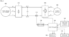
- FIG. 1 is a diagram illustrating a device for detecting an output current of an inverter according to one embodiment of the present disclosure.
- a rectifier 210 may rectify a three-phase alternating current (AC) power 400 (an R-phase, an S-phase, and a T-phase).
- the rectified power may be smoothed by a capacitor at a direct current (DC)-link configured to connect a high potential side DCP and a low potential side DCN.
- DC direct current
- the smoothed DC power may be provided to an inverter part 220, and the inverter part 220 may convert again the DC power into three-phase AC power to provide the three-phase AC power to a power system 300.
- the present disclosure relates to a device for detecting an output current provided to the inverter part 220 in the above-described inverter.
- the device for detecting an output current of an inverter may include a shunt resistor 110, a detector 120, a controller 130, a control power supplier 140, a storage 150, and a display 160.
- the shunt resistor 110 may be connected between the low potential side DCN of the DC-link, at which the capacitor is disposed, and the inverter part 220.
- the shunt resistor 110 is a resistor having very low resistance and is used for a current measurement.
- the detector 120 is connected to the shunt resistor 110 and the controller 130.
- the detector 120 may detect a current using a signal across both ends of the shunt resistor 110.
- the detector 120 may detect the current through sampling thereof and provide the detected current to the controller 130.
- the controller 130 may be connected to the detector 120, the display 160, the control power supplier 140, the storage 150, and the inverter part 220.
- the controller 130 may receive the detected current from the detector 120 using power supplied from the control power supplier 140, and may control the storage 150, the display 160, and the inverter part 220.
- the controller 130 may control a sampling timing of a current in the detector 120. Also, the controller 130 may compare a length of an effective vector regarding a switching voltage with a preset value to modulate the length of the effective vector.
- the control power supplier 140 may be connected to the controller 130 and may supply the controller 130 with power required for control.
- the storage 150 may be connected to the controller 130 and may store a delay time that is usable at a sampling timing of a current, a preset value regarding the length of the effective vector length, and the like.
- the display 160 may be connected to the controller 130, and may visually display information regarding the sampled current to a user under the control of the controller 130.
- FIG. 2 is a diagram illustrating an arrangement of switching elements connected inside the inverter part 220.
- the switching elements connected inside the inverter part 220 may include upper-stage switching elements S1, S2, and S3 respectively disposed each between output lines for three phases (a U-phase, a V-phase, and a W-phase) and the high potential side DCP of the capacitor, and lower-stage switching elements S4, S5, and S6 respectively disposed each between the output lines for the three phases (the U-phase, the V-phase, and the W-phase) and the low potential side DCN of the capacitor.
- upper-stage switching elements S1, S2, and S3 respectively disposed each between output lines for three phases (a U-phase, a V-phase, and a W-phase) and the high potential side DCP of the capacitor
- lower-stage switching elements S4, S5, and S6 respectively disposed each between the output lines for the three phases (the U-phase, the V-phase, and the W-phase) and the low potential side DCN of the capacitor.
- the switching elements disposed in the same row are connected to the output line for the same phase, and thus the upper-stage and lower-stage switching elements S1 and S4 for the U-phase will be denoted as Sa, the upper-stage and lower-stage switching elements S2 and S5 for the V-phase will be denoted Sb, and the upper-stage and lower-stage switching elements S3 and S6 for the W-phase will be denoted as Sc.
- a vector regarding a switching voltage may be represented according to a state of each of Sa, Sb, and Sc. That is, when a case in which the upper-stage switching elements are turned on is denoted as 1, and a case in which the lower-stage switching elements are turned on is denoted as 0, the switching voltage may be represented as (100), (110), and the like. At this point, (100) refers that the upper-stage switching element of Sa, the lower-stage switching element of Sb, and the lower-stage switching element of Sc are turned on. That is, (100) refers that the switching elements S1, S5, and S6 are turned on.
- FIG. 3 is a diagram illustrating dq-axis converted voltages and vectors corresponding thereto.
- V0(000), V1(100), V2(110), V3(010), V4(011), V5(001), V6(101), and V7(111), which are dq-axis converted, are illustrated.
- V0(000) and V7(111) are not defined as effective vectors since a current does not flow in the power system 300 even though the switching elements are turned on by V0(000) and V7(111).
- V1 to V6 may be defined as effective vectors
- Sectors 1 to 6 may be respectively defined by between V1 and V2, between V2 and V3, between V3 and V4, between V4 and V5, between V5 and V6, and between V6 and V1, and an output current may be detected in sections except for shaded sections.
- Table 1 represents an effective vector that is definable in each of Sectors 1 to 6, a detected current corresponding to the effective vector, and a relationship between the detected current and each of three-phase output currents Iu, Iv, and Iw.
- FIG. 4 is a diagram illustrating a pattern of a pulse width modulation (PWM) modulated switching voltage.
- PWM pulse width modulation
- the controller 130 may perform a PWM modulation on the switching voltage to secure the length of the effective vector, which is greater than the sampling time.
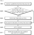
- FIG. 5 is a flowchart illustrating a method for detecting an output current of an inverter according to one embodiment of the present disclosure.
- the method for detecting an output current of an inverter according to one embodiment of the present disclosure may be performed by the device for detecting an output current of an inverter according to one embodiment of the present disclosure. Therefore, the method for detecting an output current of an inverter according to one embodiment of the present disclosure will be mainly described with the detector 120 and the controller 130 of the device for detecting an output current of an inverter.
- the controller 130 detects a length of an effective vector.
- the controller 130 compares the length of the effective vector with that of a PWM modulated effective vector. When the length of the effective vector is less than or equal to that of the PWM modulated effective vector, the process proceeds to operation S505, and otherwise, the process proceeds to operation S507.
- the length of the PWM modulated effective vector may be set in consideration of a minimum time required for securing a sampling time.
- the length of the PWM modulated effective vector may be set to be greater by 1 microseconds ( ⁇ s) than the minimum time required for sampling of a current.
- ⁇ s microseconds
- the minimum time required for securing the sampling time refers to a time including a dead time, a turn on time, and a voltage signal stabilization time when a switch is turned on or off.
- the controller 130 may perform a PWM modulation to secure a sufficient length of the effective vector. Accordingly, the controller 130 may modulate the length of the effective vector with that of the PWM modulated effective vector. That is, the controller 130 modulates the length of the effective vector with a time that is greater than a time at which the current is stabilized.
- the controller 130 may calculate a median of the length of the effective vector.
- the controller 130 may calculate the median of the length of the effective vector when the effective vector is not PWM modulated, while the controller 130 may calculate a median of the modulated effective vector when the effective vector is PWM modulated.
- the controller 130 may determine a sampling timing by applying a delay time from the median of the effective vector. In this case, the controller 130 may determine the delay time to have a value that is slightly less than a half of the length of the PWM modulated effective vector.
- the controller 130 may determine the length of the PWM modulated effective vector as 12 ⁇ s and the delay time as 5 ⁇ s.
- the length of the effective vector is 10 ⁇ s
- the effective vector is modulated with a length of 12 ⁇ s
- the sampling timing may be 11 ⁇ s to which the delay time of 5 ⁇ s is applied from 6 ⁇ s that is the median of the length of the PWM modulated effective vector.
- the present disclosure is not limited to the described above, and the delay time may be freely determined within a range that is less than the median.
- the detector 120 may sample the current by corresponding to the determined sampling timing to provide the sampled current to the controller 130.
- FIG. 6 is a diagram illustrating a sampling timing of a current when a length of an effective vector is sufficient.
- FIG. 6 there is exemplified a situation in which an error of the current may occur even though the sampling is performed after the minimum time required for a sampling (corresponding to a timing 1) from the starting point of the effective vector.
- the controller 130 determines a timing after the delay time (corresponding to a timing 2) from the median (an alternate long and short dash line) of the length of the effective vector as the sampling timing, an error of a current being detected may be reduced.
- FIG. 7 is a diagram illustrating a PWM modulation and a sampling timing of a current when a length of an effective vector is insufficient.
- the controller 130 modulates the effective vector with a length of a PWM modulated effective vector since a length of the effective vector is insufficient.
- the controller 130 modulates the effective vector with the length of the PWM modulated effective vector as well as determines a timing after a delay time (corresponding to a timing 3) from a median of the modulated effective vector as a sampling timing such that the sampling may be prevented from being performed at another effective vector, and an error may be prevented from occurring in a current value.
- the present disclosure may minimize possibility of a current detection error to accurately measure the output current provided to the inverter part.
Landscapes
- Engineering & Computer Science (AREA)
- Physics & Mathematics (AREA)
- General Physics & Mathematics (AREA)
- Power Engineering (AREA)
- Computer Networks & Wireless Communication (AREA)
- Signal Processing (AREA)
- Inverter Devices (AREA)
Abstract
Description
- The present disclosure relates to a device for detecting an output current of an inverter.
- An inverter is a typical power conversion device configured to receive and convert an alternating current (AC) power into a direct current (DC) power, and then convert again the converted DC power into AC power to control a power system.
- The inverter is used in various forms, such as a fan, a pump, an elevator, a conveying device, a production line, and the like, across the industry.
- The inverter includes a rectifier configured to rectify AC power, a capacitor of a DC-link, which is disposed between the rectifier and an inverter part and is configured to smooth the rectified AC power, and the inverter part.
- A high potential side DCP and a low potential side DCN are provided at an output stage that is connected from the DC-link to the inverter part. A shunt resistor is connected to the low potential side DCN to detect an output current.
- In detection by the shunt resistor, it is important to select a sampling timing. Since there are a dead time, a turn on time, a voltage signal stabilization time, and the like when a power switch is turned on or off due to a hardware structure of the inverter, sampling a current at such times may cause an increase of a measurement error. Therefore, the sampling of the current is performed not at a starting point of an effective vector but at a timing that is delayed by a predetermined time from the starting point thereof.
- However, even though the sampling of the current is performed after being delayed by the predetermined time from the starting point of the effective vector, a current detection error may occur due to a hardware delay factor.
- Therefore, it is an object of the present disclosure to provide a device for detecting an output current of an inverter, which is capable of preventing a current detection error even when a circuit delay factor occurs.
- To resolve the above-described objective, a device for detecting an output current of an inverter according to one embodiment of the present disclosure includes a shunt resistor connected to an output end of a capacitor of a direct current (DC) link; a detector connected to the shunt resistor and configured to detect the output current; and a controller configured to control a sampling timing of a current in the detector, wherein the controller may compare a length of an effective vector regarding a switching voltage with a predetermined value and modulate the length of the effective vector.
- In one embodiment of the present disclosure, the shunt resistor may be connected to a low potential side.
- In one embodiment of the present disclosure, the controller may sample the current at a timing that is delayed by a set time based on a median of the effective vector.
- In one embodiment of the present disclosure, the controller may modulate the length of the effective vector with a value that is greater than a time at which a current by the effective vector is stabilized.
- In one embodiment of the present disclosure, the controller may determine the delayed timing as a value that is greater than a half of the time at which the current by the effective vector is stabilized.
- In accordance with the present disclosure, there is an effect capable of minimizing possibility of a current detection error to accurately detect an output current provided to an inverter part.
-
-
FIG. 1 is a diagram illustrating a device for detecting an output current of an inverter according to one embodiment of the present disclosure. -
FIG. 2 is a diagram illustrating an arrangement of switching elements connected to an inverter part. -
FIG. 3 is a diagram illustrating dq-axis converted voltages and vectors corresponding thereto. -
FIG. 4 is a diagram illustrating a pattern of a pulse width modulation (PWM) modulated switching voltage. -
FIG. 5 is a flowchart illustrating a method for detecting an output current of an inverter according to one embodiment of the present disclosure. -
FIG. 6 is a diagram illustrating a sampling timing of a current when a length of an effective vector is sufficient. -
FIG. 7 is a diagram illustrating a PWM modulation and a sampling timing of a current when a length of an effective vector is insufficient. - The above objects, features and advantages will become apparent from the detailed description with reference to the accompanying drawings. Embodiments are described in sufficient detail to enable those skilled in the art to easily practice the technical idea of the present disclosure. Detailed descriptions of well known functions or configurations may be omitted in order not to unnecessarily obscure the gist of the present disclosure. Hereinafter, embodiments of the present disclosure will be described in detail with reference to the accompanying drawings. Throughout the drawings, like reference numerals refer to like elements.
- Hereinafter, one preferred embodiment according to the present disclosure will be described in detail with reference to the accompanying drawings.
-
FIG. 1 is a diagram illustrating a device for detecting an output current of an inverter according to one embodiment of the present disclosure. - Referring to
FIG. 1 , arectifier 210 may rectify a three-phase alternating current (AC) power 400 (an R-phase, an S-phase, and a T-phase). The rectified power may be smoothed by a capacitor at a direct current (DC)-link configured to connect a high potential side DCP and a low potential side DCN. - The smoothed DC power may be provided to an
inverter part 220, and theinverter part 220 may convert again the DC power into three-phase AC power to provide the three-phase AC power to apower system 300. - The present disclosure relates to a device for detecting an output current provided to the
inverter part 220 in the above-described inverter. - The device for detecting an output current of an inverter may include a
shunt resistor 110, adetector 120, acontroller 130, acontrol power supplier 140, astorage 150, and adisplay 160. - The
shunt resistor 110 may be connected between the low potential side DCN of the DC-link, at which the capacitor is disposed, and theinverter part 220. - The
shunt resistor 110 is a resistor having very low resistance and is used for a current measurement. - The
detector 120 is connected to theshunt resistor 110 and thecontroller 130. - The
detector 120 may detect a current using a signal across both ends of theshunt resistor 110. Thedetector 120 may detect the current through sampling thereof and provide the detected current to thecontroller 130. - The
controller 130 may be connected to thedetector 120, thedisplay 160, thecontrol power supplier 140, thestorage 150, and theinverter part 220. - The
controller 130 may receive the detected current from thedetector 120 using power supplied from thecontrol power supplier 140, and may control thestorage 150, thedisplay 160, and theinverter part 220. - The
controller 130 may control a sampling timing of a current in thedetector 120. Also, thecontroller 130 may compare a length of an effective vector regarding a switching voltage with a preset value to modulate the length of the effective vector. - The
control power supplier 140 may be connected to thecontroller 130 and may supply thecontroller 130 with power required for control. - The
storage 150 may be connected to thecontroller 130 and may store a delay time that is usable at a sampling timing of a current, a preset value regarding the length of the effective vector length, and the like. - The
display 160 may be connected to thecontroller 130, and may visually display information regarding the sampled current to a user under the control of thecontroller 130. -
FIG. 2 is a diagram illustrating an arrangement of switching elements connected inside theinverter part 220. - Referring to
FIG. 2 , the switching elements connected inside theinverter part 220 may include upper-stage switching elements S1, S2, and S3 respectively disposed each between output lines for three phases (a U-phase, a V-phase, and a W-phase) and the high potential side DCP of the capacitor, and lower-stage switching elements S4, S5, and S6 respectively disposed each between the output lines for the three phases (the U-phase, the V-phase, and the W-phase) and the low potential side DCN of the capacitor. - In the present description, the switching elements disposed in the same row are connected to the output line for the same phase, and thus the upper-stage and lower-stage switching elements S1 and S4 for the U-phase will be denoted as Sa, the upper-stage and lower-stage switching elements S2 and S5 for the V-phase will be denoted Sb, and the upper-stage and lower-stage switching elements S3 and S6 for the W-phase will be denoted as Sc.
- A vector regarding a switching voltage may be represented according to a state of each of Sa, Sb, and Sc. That is, when a case in which the upper-stage switching elements are turned on is denoted as 1, and a case in which the lower-stage switching elements are turned on is denoted as 0, the switching voltage may be represented as (100), (110), and the like. At this point, (100) refers that the upper-stage switching element of Sa, the lower-stage switching element of Sb, and the lower-stage switching element of Sc are turned on. That is, (100) refers that the switching elements S1, S5, and S6 are turned on.
-
FIG. 3 is a diagram illustrating dq-axis converted voltages and vectors corresponding thereto. - Referring to
FIG. 3 , V0(000), V1(100), V2(110), V3(010), V4(011), V5(001), V6(101), and V7(111), which are dq-axis converted, are illustrated. - V0(000) and V7(111) are not defined as effective vectors since a current does not flow in the
power system 300 even though the switching elements are turned on by V0(000) and V7(111). - V1 to V6 may be defined as effective vectors,
Sectors 1 to 6 may be respectively defined by between V1 and V2, between V2 and V3, between V3 and V4, between V4 and V5, between V5 and V6, and between V6 and V1, and an output current may be detected in sections except for shaded sections. - The following Table 1 represents an effective vector that is definable in each of
Sectors 1 to 6, a detected current corresponding to the effective vector, and a relationship between the detected current and each of three-phase output currents Iu, Iv, and Iw.[Table 1] Sector Effective Vector Detected Current Iu Iv Iw 1 100 Iu = IDC IDC -(Iu+Iw) - IDC 110 Iw = - IDC 2 010 Iu = IDC -(Iv+Iw) IDC - IDC 110 Iw = - IDC 3 010 Iu = IDC -IDC IDC -(Iu+Iv) 011 Iw = - IDC 4 001 Iu = IDC -IDC -(Iu+Iw) IDC 011 Iw = - IDC 5 001 Iu = IDC -(Iv+Iw) - IDC IDC 101 Iw = - IDC 6 100 Iu = IDC IDC -IDC -(Iu+Iv) 101 Iw = -IDC - For example, in
Sector 1, when a current IDC flowing on theshunt resistor 110 with the effective vector (100) is measured, it can be seen that Iu = IDC, the current Iu flowing at the U-phase. Also, when the current IDC flowing on theshunt resistor 110 with the effective vector (110) is measured, a current Iw flowing at the W-phase may be obtained from Iw = -IDC. When the current Iu flowing at the U-phase and the current Iw flowing at the W-phase are obtained inSector 1, a current flowing at the V-phase may be obtained from a relationship of Iu + Iv + Iw = 0 by assuming that the three phases of the U-phase, the W-phase, and the V-phase are in equilibrium. -
FIG. 4 is a diagram illustrating a pattern of a pulse width modulation (PWM) modulated switching voltage. - Referring to
FIG. 4 , when a length (a temporal length) of an effective vector is small and thus a sampling time of a current may not be secured, thecontroller 130 may perform a PWM modulation on the switching voltage to secure the length of the effective vector, which is greater than the sampling time. -
FIG. 5 is a flowchart illustrating a method for detecting an output current of an inverter according to one embodiment of the present disclosure. - The method for detecting an output current of an inverter according to one embodiment of the present disclosure may be performed by the device for detecting an output current of an inverter according to one embodiment of the present disclosure. Therefore, the method for detecting an output current of an inverter according to one embodiment of the present disclosure will be mainly described with the
detector 120 and thecontroller 130 of the device for detecting an output current of an inverter. - In operation S501, the
controller 130 detects a length of an effective vector. - In operation S503, the
controller 130 compares the length of the effective vector with that of a PWM modulated effective vector. When the length of the effective vector is less than or equal to that of the PWM modulated effective vector, the process proceeds to operation S505, and otherwise, the process proceeds to operation S507. - Here, the length of the PWM modulated effective vector may be set in consideration of a minimum time required for securing a sampling time. For example, the length of the PWM modulated effective vector may be set to be greater by 1 microseconds (µs) than the minimum time required for sampling of a current. However, the present disclosure is not limited to the described above.
- Meanwhile, the minimum time required for securing the sampling time refers to a time including a dead time, a turn on time, and a voltage signal stabilization time when a switch is turned on or off.
- In operation S505, the
controller 130 may perform a PWM modulation to secure a sufficient length of the effective vector. Accordingly, thecontroller 130 may modulate the length of the effective vector with that of the PWM modulated effective vector. That is, thecontroller 130 modulates the length of the effective vector with a time that is greater than a time at which the current is stabilized. - In operation S507, the
controller 130 may calculate a median of the length of the effective vector. Thecontroller 130 may calculate the median of the length of the effective vector when the effective vector is not PWM modulated, while thecontroller 130 may calculate a median of the modulated effective vector when the effective vector is PWM modulated. - In operation S509, the
controller 130 may determine a sampling timing by applying a delay time from the median of the effective vector. In this case, thecontroller 130 may determine the delay time to have a value that is slightly less than a half of the length of the PWM modulated effective vector. - For example, when the minimum time required for a sampling is 10 µs, the
controller 130 may determine the length of the PWM modulated effective vector as 12 µs and the delay time as 5 µs. In this case, when the length of the effective vector is 10 µs, the effective vector is modulated with a length of 12 µs, and the sampling timing may be 11 µs to which the delay time of 5 µs is applied from 6 µs that is the median of the length of the PWM modulated effective vector. However, the present disclosure is not limited to the described above, and the delay time may be freely determined within a range that is less than the median. - In operation S511, the
detector 120 may sample the current by corresponding to the determined sampling timing to provide the sampled current to thecontroller 130. -
FIG. 6 is a diagram illustrating a sampling timing of a current when a length of an effective vector is sufficient. - Referring to
FIG. 6 , there is exemplified a situation in which an error of the current may occur even though the sampling is performed after the minimum time required for a sampling (corresponding to a timing ①) from the starting point of the effective vector. - However, as in one embodiment of the present disclosure, since the
controller 130 determines a timing after the delay time (corresponding to a timing ②) from the median (an alternate long and short dash line) of the length of the effective vector as the sampling timing, an error of a current being detected may be reduced. -
FIG. 7 is a diagram illustrating a PWM modulation and a sampling timing of a current when a length of an effective vector is insufficient. - Referring to
FIG. 7 , it can be seen that thecontroller 130 modulates the effective vector with a length of a PWM modulated effective vector since a length of the effective vector is insufficient. - The
controller 130 modulates the effective vector with the length of the PWM modulated effective vector as well as determines a timing after a delay time (corresponding to a timing ③) from a median of the modulated effective vector as a sampling timing such that the sampling may be prevented from being performed at another effective vector, and an error may be prevented from occurring in a current value. - Through the described above, the present disclosure may minimize possibility of a current detection error to accurately measure the output current provided to the inverter part.
- The present disclosure described above may be variously substituted, altered, and modified by those skilled in the art to which the present disclosure pertains without departing from the scope and spirit of the present disclosure. Therefore, the present disclosure is not limited to the above-mentioned exemplary embodiments and the accompanying drawings.
Claims (5)
- A device for detecting an output current of an inverter configured to control a power system (300), comprising:a shunt resistor (110) connected to an output end of a capacitor of a direct current (DC) link;a detector (120) connected to the shunt resistor (110) and configured to detect the output current; anda controller (130) configured to control a sampling timing of a current in the detector (120),wherein the controller (130) compares a length of an effective vector regarding a switching voltage with a preset value and modulates the length of the effective vector.
- The device of claim 1, wherein the shunt resistor (110) is connected to a low potential side.
- The device of claim 1 or 2, wherein the controller (130) samples the current at a timing that is delayed by a set time based on a median of the length of the effective vector.
- The device of claim 1 or 2, wherein the controller (130) modulates the length of the effective vector with a value that is greater than a time at which a current by the effective vector is stabilized.
- The device of claim 3, wherein the controller (130) determines the delayed timing as a value that is greater than a half of the time at which the current by the effective vector is stabilized.
Applications Claiming Priority (1)
| Application Number | Priority Date | Filing Date | Title |
|---|---|---|---|
| KR1020170035041A KR101922998B1 (en) | 2017-03-21 | 2017-03-21 | Sensing Device for output current of inverter |
Publications (1)
| Publication Number | Publication Date |
|---|---|
| EP3379715A1 true EP3379715A1 (en) | 2018-09-26 |
Family
ID=60935738
Family Applications (1)
| Application Number | Title | Priority Date | Filing Date |
|---|---|---|---|
| EP18150437.4A Withdrawn EP3379715A1 (en) | 2017-03-21 | 2018-01-05 | Device for detecting output current of inverter |
Country Status (5)
| Country | Link |
|---|---|
| US (1) | US10175274B2 (en) |
| EP (1) | EP3379715A1 (en) |
| JP (1) | JP6487074B2 (en) |
| KR (1) | KR101922998B1 (en) |
| CN (1) | CN108627684B (en) |
Families Citing this family (9)
| Publication number | Priority date | Publication date | Assignee | Title |
|---|---|---|---|---|
| EP3464146A1 (en) * | 2016-05-31 | 2019-04-10 | Inventio AG | Elevator drive control during power disruption |
| US10418912B2 (en) | 2017-12-21 | 2019-09-17 | Silanna Asia Pte Ltd | Power converter with active clamp |
| US10461626B1 (en) | 2019-01-14 | 2019-10-29 | Silanna Asia Pte Ltd | Active clamp circuit |
| CN110445407B (en) * | 2019-08-19 | 2021-02-12 | 电子科技大学 | A rectifier circuit for starting a generator integrated machine |
| KR102181652B1 (en) * | 2019-10-10 | 2020-11-23 | 엘지전자 주식회사 | Apparatus for controlling motor and motor control method thereof |
| KR102779845B1 (en) * | 2019-12-03 | 2025-03-12 | 엘지이노텍 주식회사 | Apparatus for detecting current of 3-Phase inverter and method thereof |
| KR102281633B1 (en) * | 2019-12-03 | 2021-07-23 | 엘에스일렉트릭(주) | Apparatus and method for controlling inverter |
| KR102698331B1 (en) * | 2021-12-14 | 2024-08-26 | 주식회사 현대케피코 | Method for measuring 3-phase current |
| KR20260006970A (en) * | 2024-07-05 | 2026-01-13 | 삼성전자주식회사 | Motor driving apparatus and control method thereof |
Citations (3)
| Publication number | Priority date | Publication date | Assignee | Title |
|---|---|---|---|---|
| US20040195995A1 (en) * | 2003-01-20 | 2004-10-07 | Jean Quirion | Method and apparatus for reconstructing motor current from DC bus current |
| EP1863160A2 (en) * | 2006-06-01 | 2007-12-05 | Vacon Oyj | Measurement of the current of a frequency converter |
| EP3062428A2 (en) * | 2015-02-28 | 2016-08-31 | Rockwell Automation Technologies, Inc. | Inverter phase current reconstruction apparatus and methods |
Family Cites Families (15)
| Publication number | Priority date | Publication date | Assignee | Title |
|---|---|---|---|---|
| JP3951516B2 (en) | 1999-09-14 | 2007-08-01 | 株式会社明電舎 | Inverter |
| EP2045905B1 (en) | 2001-09-29 | 2013-06-12 | Daikin Industries, Ltd. | Phase current detection method, inverter control method, motor control method, and apparatuses used in these methods |
| JP2004064903A (en) * | 2002-07-30 | 2004-02-26 | Hitachi Ltd | Synchronous motor control device and device using the same |
| KR20070072088A (en) * | 2005-12-30 | 2007-07-04 | 엘지전자 주식회사 | Inverter control device and method |
| JP4759422B2 (en) * | 2006-03-27 | 2011-08-31 | 日立アプライアンス株式会社 | Power converter system and washing machine using the same |
| KR20080060847A (en) | 2006-12-27 | 2008-07-02 | 삼성전자주식회사 | Phase current detection method of inverter circuit |
| JP5314989B2 (en) * | 2008-10-02 | 2013-10-16 | 本田技研工業株式会社 | Motor phase current estimation device |
| JP5325561B2 (en) | 2008-12-22 | 2013-10-23 | 株式会社日立製作所 | Three-phase AC motor control device and control method thereof |
| JP5292363B2 (en) * | 2010-06-30 | 2013-09-18 | 株式会社日立製作所 | AC motor control device and control method |
| EP2574947A1 (en) | 2011-09-30 | 2013-04-03 | ABB Technology AG | A method of determining stationary signals for the diagnostics of an electromechanical system |
| KR101261793B1 (en) * | 2012-02-06 | 2013-05-07 | 엘에스산전 주식회사 | Apparatus for controlling phase current detection in inverter |
| JP5839011B2 (en) | 2013-09-18 | 2016-01-06 | 株式会社デンソー | Power conversion device and electric power steering device using the same |
| JP5892394B2 (en) * | 2014-01-28 | 2016-03-23 | 株式会社デンソー | Power conversion device and electric power steering device using the same |
| KR101993195B1 (en) * | 2015-04-09 | 2019-06-26 | 엘에스산전 주식회사 | A method for detecting a ground fault of an inverter |
| JP6341165B2 (en) | 2015-09-01 | 2018-06-13 | 株式会社安川電機 | Power conversion device, phase current detection device, and phase current detection method |
-
2017
- 2017-03-21 KR KR1020170035041A patent/KR101922998B1/en active Active
-
2018
- 2018-01-05 EP EP18150437.4A patent/EP3379715A1/en not_active Withdrawn
- 2018-01-09 US US15/865,954 patent/US10175274B2/en active Active
- 2018-01-12 JP JP2018003553A patent/JP6487074B2/en not_active Expired - Fee Related
- 2018-01-17 CN CN201810045008.8A patent/CN108627684B/en not_active Expired - Fee Related
Patent Citations (3)
| Publication number | Priority date | Publication date | Assignee | Title |
|---|---|---|---|---|
| US20040195995A1 (en) * | 2003-01-20 | 2004-10-07 | Jean Quirion | Method and apparatus for reconstructing motor current from DC bus current |
| EP1863160A2 (en) * | 2006-06-01 | 2007-12-05 | Vacon Oyj | Measurement of the current of a frequency converter |
| EP3062428A2 (en) * | 2015-02-28 | 2016-08-31 | Rockwell Automation Technologies, Inc. | Inverter phase current reconstruction apparatus and methods |
Also Published As
| Publication number | Publication date |
|---|---|
| KR101922998B1 (en) | 2018-11-28 |
| CN108627684B (en) | 2020-10-02 |
| KR20180106545A (en) | 2018-10-01 |
| JP2018161042A (en) | 2018-10-11 |
| CN108627684A (en) | 2018-10-09 |
| US10175274B2 (en) | 2019-01-08 |
| US20180275175A1 (en) | 2018-09-27 |
| JP6487074B2 (en) | 2019-03-20 |
Similar Documents
| Publication | Publication Date | Title |
|---|---|---|
| US10175274B2 (en) | Device for detecting output current of inverter | |
| US9160161B2 (en) | System and method for ground fault detection and protection in adjustable speed drives | |
| US8645087B2 (en) | Measuring of earth fault current | |
| US9846190B2 (en) | Motor drive device including function to detect failure in insulation resistance deterioration detection unit of motor, and failure detection method | |
| EP2682769A1 (en) | Apparatus for diagnosing DC link capacitor of inverter | |
| AU2016324266B2 (en) | Inverter substrate, method for determining connection sequence, and method for determining open phase | |
| KR20180083931A (en) | Uninterruptible power supply | |
| US20170063252A1 (en) | Power conversion apparatus, phase current detection apparatus, and phase current detection method | |
| US20190162773A1 (en) | Motor driving device and measuring method | |
| US11611286B2 (en) | Method for determining rectifier-stage output current or grid-side currents of a frequency converter | |
| KR102036578B1 (en) | Apparatus for detecting output phase open in inverter | |
| US20240223071A1 (en) | Switching module | |
| US12038486B2 (en) | Inverter system capable of detecting output ground fault and output ground fault detection method using same | |
| Wolbank et al. | Scheme to reconstruct phase current information of inverter fed AC drives | |
| KR20120028429A (en) | Output current detection device of 3-phase motor drive using wire-wounded resistor of motor | |
| US20210050770A1 (en) | Short-circuit-proof inverter having a direct current control | |
| JP5471498B2 (en) | Power converter | |
| JP3144075B2 (en) | AC motor constant measurement method | |
| JP2000262087A5 (en) | ||
| JPH0547074B2 (en) | ||
| KR20240148506A (en) | Power conversion device and control method of thereof | |
| KR20200137792A (en) | Power transforming apparatus and controlling method thereof | |
| JPS5851777A (en) | Converter ignition control device |
Legal Events
| Date | Code | Title | Description |
|---|---|---|---|
| PUAI | Public reference made under article 153(3) epc to a published international application that has entered the european phase |
Free format text: ORIGINAL CODE: 0009012 |
|
| STAA | Information on the status of an ep patent application or granted ep patent |
Free format text: STATUS: THE APPLICATION HAS BEEN PUBLISHED |
|
| AK | Designated contracting states |
Kind code of ref document: A1 Designated state(s): AL AT BE BG CH CY CZ DE DK EE ES FI FR GB GR HR HU IE IS IT LI LT LU LV MC MK MT NL NO PL PT RO RS SE SI SK SM TR |
|
| AX | Request for extension of the european patent |
Extension state: BA ME |
|
| STAA | Information on the status of an ep patent application or granted ep patent |
Free format text: STATUS: REQUEST FOR EXAMINATION WAS MADE |
|
| 17P | Request for examination filed |
Effective date: 20190322 |
|
| RBV | Designated contracting states (corrected) |
Designated state(s): AL AT BE BG CH CY CZ DE DK EE ES FI FR GB GR HR HU IE IS IT LI LT LU LV MC MK MT NL NO PL PT RO RS SE SI SK SM TR |
|
| STAA | Information on the status of an ep patent application or granted ep patent |
Free format text: STATUS: EXAMINATION IS IN PROGRESS |
|
| 17Q | First examination report despatched |
Effective date: 20210317 |
|
| STAA | Information on the status of an ep patent application or granted ep patent |
Free format text: STATUS: THE APPLICATION HAS BEEN WITHDRAWN |
|
| 18W | Application withdrawn |
Effective date: 20221222 |