EP3379656A1 - Three-dimensional converter - Google Patents
Three-dimensional converter Download PDFInfo
- Publication number
- EP3379656A1 EP3379656A1 EP17741126.1A EP17741126A EP3379656A1 EP 3379656 A1 EP3379656 A1 EP 3379656A1 EP 17741126 A EP17741126 A EP 17741126A EP 3379656 A1 EP3379656 A1 EP 3379656A1
- Authority
- EP
- European Patent Office
- Prior art keywords
- clapboard
- conductive sheet
- dimensional
- plug bush
- wire plug
- Prior art date
- Legal status (The legal status is an assumption and is not a legal conclusion. Google has not performed a legal analysis and makes no representation as to the accuracy of the status listed.)
- Granted
Links
- 230000001681 protective effect Effects 0.000 claims description 11
- 230000007246 mechanism Effects 0.000 claims description 9
- 210000002435 tendon Anatomy 0.000 claims description 8
- 238000009434 installation Methods 0.000 claims description 6
- 238000009413 insulation Methods 0.000 description 5
- 238000003466 welding Methods 0.000 description 4
- RYGMFSIKBFXOCR-UHFFFAOYSA-N Copper Chemical compound [Cu] RYGMFSIKBFXOCR-UHFFFAOYSA-N 0.000 description 2
- 229910052802 copper Inorganic materials 0.000 description 2
- 239000010949 copper Substances 0.000 description 2
- WABPQHHGFIMREM-UHFFFAOYSA-N lead(0) Chemical compound [Pb] WABPQHHGFIMREM-UHFFFAOYSA-N 0.000 description 2
- 238000005476 soldering Methods 0.000 description 2
- 238000009826 distribution Methods 0.000 description 1
- 238000004519 manufacturing process Methods 0.000 description 1
- 239000000463 material Substances 0.000 description 1
- 230000000007 visual effect Effects 0.000 description 1
Images


Classifications
-
- H—ELECTRICITY
- H01—ELECTRIC ELEMENTS
- H01R—ELECTRICALLY-CONDUCTIVE CONNECTIONS; STRUCTURAL ASSOCIATIONS OF A PLURALITY OF MUTUALLY-INSULATED ELECTRICAL CONNECTING ELEMENTS; COUPLING DEVICES; CURRENT COLLECTORS
- H01R25/00—Coupling parts adapted for simultaneous co-operation with two or more identical counterparts, e.g. for distributing energy to two or more circuits
- H01R25/003—Coupling parts adapted for simultaneous co-operation with two or more identical counterparts, e.g. for distributing energy to two or more circuits the coupling part being secured only to wires or cables
-
- H—ELECTRICITY
- H01—ELECTRIC ELEMENTS
- H01R—ELECTRICALLY-CONDUCTIVE CONNECTIONS; STRUCTURAL ASSOCIATIONS OF A PLURALITY OF MUTUALLY-INSULATED ELECTRICAL CONNECTING ELEMENTS; COUPLING DEVICES; CURRENT COLLECTORS
- H01R13/00—Details of coupling devices of the kinds covered by groups H01R12/70 or H01R24/00 - H01R33/00
- H01R13/46—Bases; Cases
- H01R13/502—Bases; Cases composed of different pieces
- H01R13/506—Bases; Cases composed of different pieces assembled by snap action of the parts
-
- H—ELECTRICITY
- H01—ELECTRIC ELEMENTS
- H01R—ELECTRICALLY-CONDUCTIVE CONNECTIONS; STRUCTURAL ASSOCIATIONS OF A PLURALITY OF MUTUALLY-INSULATED ELECTRICAL CONNECTING ELEMENTS; COUPLING DEVICES; CURRENT COLLECTORS
- H01R13/00—Details of coupling devices of the kinds covered by groups H01R12/70 or H01R24/00 - H01R33/00
- H01R13/648—Protective earth or shield arrangements on coupling devices, e.g. anti-static shielding
-
- H—ELECTRICITY
- H01—ELECTRIC ELEMENTS
- H01R—ELECTRICALLY-CONDUCTIVE CONNECTIONS; STRUCTURAL ASSOCIATIONS OF A PLURALITY OF MUTUALLY-INSULATED ELECTRICAL CONNECTING ELEMENTS; COUPLING DEVICES; CURRENT COLLECTORS
- H01R24/00—Two-part coupling devices, or either of their cooperating parts, characterised by their overall structure
- H01R24/20—Coupling parts carrying sockets, clips or analogous contacts and secured only to wire or cable
- H01R24/22—Coupling parts carrying sockets, clips or analogous contacts and secured only to wire or cable with additional earth or shield contacts
-
- H—ELECTRICITY
- H01—ELECTRIC ELEMENTS
- H01R—ELECTRICALLY-CONDUCTIVE CONNECTIONS; STRUCTURAL ASSOCIATIONS OF A PLURALITY OF MUTUALLY-INSULATED ELECTRICAL CONNECTING ELEMENTS; COUPLING DEVICES; CURRENT COLLECTORS
- H01R31/00—Coupling parts supported only by co-operation with counterpart
- H01R31/02—Intermediate parts for distributing energy to two or more circuits in parallel, e.g. splitter
-
- H—ELECTRICITY
- H01—ELECTRIC ELEMENTS
- H01R—ELECTRICALLY-CONDUCTIVE CONNECTIONS; STRUCTURAL ASSOCIATIONS OF A PLURALITY OF MUTUALLY-INSULATED ELECTRICAL CONNECTING ELEMENTS; COUPLING DEVICES; CURRENT COLLECTORS
- H01R13/00—Details of coupling devices of the kinds covered by groups H01R12/70 or H01R24/00 - H01R33/00
- H01R13/44—Means for preventing access to live contacts
- H01R13/447—Shutter or cover plate
-
- H—ELECTRICITY
- H01—ELECTRIC ELEMENTS
- H01R—ELECTRICALLY-CONDUCTIVE CONNECTIONS; STRUCTURAL ASSOCIATIONS OF A PLURALITY OF MUTUALLY-INSULATED ELECTRICAL CONNECTING ELEMENTS; COUPLING DEVICES; CURRENT COLLECTORS
- H01R13/00—Details of coupling devices of the kinds covered by groups H01R12/70 or H01R24/00 - H01R33/00
- H01R13/46—Bases; Cases
- H01R13/514—Bases; Cases composed as a modular blocks or assembly, i.e. composed of co-operating parts provided with contact members or holding contact members between them
-
- H—ELECTRICITY
- H01—ELECTRIC ELEMENTS
- H01R—ELECTRICALLY-CONDUCTIVE CONNECTIONS; STRUCTURAL ASSOCIATIONS OF A PLURALITY OF MUTUALLY-INSULATED ELECTRICAL CONNECTING ELEMENTS; COUPLING DEVICES; CURRENT COLLECTORS
- H01R13/00—Details of coupling devices of the kinds covered by groups H01R12/70 or H01R24/00 - H01R33/00
- H01R13/66—Structural association with built-in electrical component
- H01R13/665—Structural association with built-in electrical component with built-in electronic circuit
Definitions
- the present disclosure relates to the field of electrical equipment, and in particular, relates to a three-dimensional convertor.
- a three-dimensional convertor is also called a magic cube socket.
- an individual conductive sheet is equipped to each jack on each side of the convertor, and then the jack and its corresponding conductive sheet are assembled to form a plug bush module on each side of the convertor.
- the plug bush modules are conducted among each other by means of welding flexible wires or other materials; however, this practice results in too many assembly parts and a complex manufacturing method.
- the conductive sheets with the same polar inside the plug bush module are welded together through wires and copper bars, a pseudo soldering or a false welding will be caused.
- the Chinese application No. 201420868334.6 for utility model describes a three-dimensional multi-side socket unit and a combined socket.
- Said three-dimensional multi-side socket unit comprises a plug, an inner core assembly and a cubic outer box.
- the cubic outer box covers the outside of the inner core assembly.
- Said inner core assembly comprises a live wire integral elastic piece, an A cavity frame, an earth wire integral elastic piece, a B cavity frame, a naught wire integral elastic piece, and a side elastic piece terminal.
- Said earth wire integral elastic piece is clamped between the A cavity frame and the B cavity frame.
- the live wire integral elastic piece is installed on the A cavity frame, while the earth wire integral elastic piece is installed on the B cavity frame.
- the multi-side socket unit solves the problem of the pseudo soldering or the false welding resulted by welding the conductive sheets with the same polar inside the magic cube socket together through wires and copper bars. But, the assembly of the multi-side socket unit with the above structure is difficult when which is assembled, as the integral elastic pieces of the inner core assembly easily fall off from the corresponding cavity frames. Moreover, as the cubic outer box is divided into three parts, more steps of assembly will be involved.
- the disclosure is intended to provide a three-dimensional convertor with less assembly steps, which is easy to be assembled.
- a three-dimensional convertor comprises a housing and a socket interior provided inside the housing; wherein, the socket interior comprises clapboards and a live plug bush conductive sheet, a naught wire plug bush conductive sheet and an earth plug bush conductive sheet; wherein, the clapboards comprise a first clapboard, a second clapboard, a third clapboard and a fourth clapboard which are sequentially stacked; the naught wire plug bush conductive sheet is provided between the first clapboard and the second clapboard, the earth plug bush conductive sheet is provided between the second clapboard and the third clapboard, and the live wire plug bush conductive sheet is provided between the third clapboard and the fourth clapboard; the housing comprises at least two jack surfaces on each of which jacks are provided, each jack corresponds to one of the live wire plug bush conductive sheet, the naught wire plug bush conductive sheet and the earth wire plug bush conductive sheet.
- buckle arms which can be buckled with each other and are provided between the first clapboard and the fourth clapboard, and each clapboard and its corresponding conductive sheet are pressed against each other when the buckle arm of the first clapboard is buckled with that of the fourth clapboard.
- a clamping slot is provided on the free end of the buckle arm on the first clapboard, a clamping projection to buckle with the clamping slot is provided on the free end of the buckle arm on the fourth clapboard; or, a clamping slot is provided on the free end of the buckle arm on the fourth clapboard, a clamping projection to buckle with the clamping slot is provided on the free end of the buckle arm on the first clapboard.
- the buckle arms surround the peripheries of the second clapboard and the third clapboard; or, the buckle arms passes through the second clapboard and the third clapboard.
- a first positioning post is provided on the first clapboard or the fourth clapboard, and a first positioning hole that engages with the first positioning post is provided on other clapboards except the one provided with the first positioning post.
- a screwed hole to lock up with a screw is provided on the free end of positioning post, and a counter bore to accommodate the screw is provided on the clapboard where the free end of positioning post is located.
- a circuit board is extended from a surface of the first clapboard far away from the second clapboard; or, a circuit board is extended from a surface of the fourth clapboard far away from the third clapboard.
- the circuit board comprises a USB circuit board and/or a heavy-current switch circuit board.
- a surface of the clapboard provided with the electric circuit board is provided with isolating tendons configured to insulate the heavy-current switch circuit board and the USB circuit board (61).
- a threading hole configured to lead conductive cables out is provided on one side surface of the housing, and a wiring slot is recessed inward in a side surface of the socket interior that corresponds to the threading hole.
- a first wiring pin is provided on the live wire plug bush conductive sheet
- a second wiring pin is provided on the naught wire plug bush conductive sheet
- the first wiring pin and the second wiring pin are both provided in the wiring slot.
- a first press block is provided on a side surface of the socket interior opposing the threading hole
- a second press block is provided under the threading hole on the inner side of the housing, and the first press block and the second press block contact with each other when the socket interior is installed in the housing.
- the earth wire plug bush conductive sheet is provided with the third wiring pin, and the third wiring pin is bent toward the earth wire plug bush conductive sheet, passing through the third clapboard and the fourth clapboard, and being exposed outside the fourth clapboard. Or, the third wiring pin passes through the first clapboard and the second clapboard and is exposed outside the first clapboard.
- said housing comprises a lower housing with one open mouth, and an upper housing cover that can seal the open mouth, and the threaded hole is provided on one lateral of the lower housing.
- the base of the lower housing opposing the upper housing cover is the bearing surface, and the other three laterals of the lower housing except the one provided with the threaded hole are all jack surfaces with ports provided on each jack surface.
- a protective door module is provided between the socket interior and the inner side of the housing with the jack, and the protective door module is configured to protect the jack.
- a sticking post is provided on a side surface of the socket interior opposing the inner side of the housing, and the sticking post is configured to orientate the protective door module.
- a clamping joint is provided on a side of the isolating tendon facing towards the upper cover, the clamping joint extends towards the upper cover, and a blind groove that engages with the clamping joint is provided on a corresponding inner surface of the upper housing lid.
- the first or the fourth clapboard installed in the circuit board is further provided with an insulation board that separates the USB circuit board and the heavy-current switch circuit board.
- a positioning mechanism is provided between each clapboard and each corresponding conductive sheet which are stacked alternatively, and the positioning mechanism is configured to orientate each conductive sheet to each corresponding clapboard.
- a second positioning post provided on the clapboard, and a second positioning hole respectively provided on the live wire plug bush conductive sheet, the naught wire plug bush conductive sheet and the earth wire plug bush conductive sheet, second positioning holes are one to one corresponding to and engage with second positioning posts.
- each of the plug bush conductive sheets in the present disclosure is clamped between two corresponding clapboards, and when the 3 dimensional convertor is assembled, it is only required that to make each plug bush conductive sheet and each clapboard to be alternatively stacked and compressed tightly, and then to form an integral socket interior by locking up the buckle structure between the first clapboard and the fourth clapboard, and finally to complete the assembly by put the socket interior into the housing.
- the difficulty of assembly is reduced and the efficiency of assembly is improved.
- some wiring slots and press blocks are provided on the clapboards, so as to make it easier to route wires after the wires has been weld to wiring pins of each plug bush conductive sheet.
- the arrangement that the threading hole in the housing being directly opposed to the press block reduces the length of the wires, increases the utilization rate of the inner space of the 3D convertor and meanwhile relatively reduces the overall dimension of the 3D convertor.
- a 3D convertor comprises a socket interior within a housing.
- the socket interior comprises clapboards and plug bush conductive sheets.
- the clapboards include a first clapboard 11, a second clapboard 12, a third clapboard 13 and a fourth clapboard 14 which are sequentially stacked.
- the plug bush conductive sheets comprise a live wire plug bush conductive sheet 21 arranged between the first clapboard 11 and the second clapboard 12, an earth wire plug bush conductive sheet 23 arranged between the second clapboard 12 and the third clapboard 13, and a naught wire plug bush conductive sheet 22 arranged between the third clapboard 13 and the fourth clapboard 14.
- a buckle structure is provided between the first clapboard 11 and the fourth clapboard 14 which are at the opposite ends, to form a tight integral socket interior by mutually stacking each clapboard and each plug bush conductive sheet and making them press against each other.
- the buckle structure may comprise a buckle arm 111 provided at the edge of the first clapboard 11 and extending towards the fourth clapboard 14, with a clamping slot 1111 provided on the buckle arm 111, and a clamping projection 141 that engages with the clamping slot 1111 of the buckle arm 111 provided on the fourth clapboard 14. It can be understood that the buckle arm could also be provided on the fourth clapboard 14, while the clamping projection 141 could be provided on the first clapboard 11.
- buckle arms are provided on the fourth clapboard 14 but not in a straight line.
- the buckle arms respectively surrounds the peripheries of the second clapboard 12 and the third clapboard 13 after the socket interior is assembled; of course, it can be understood that the buckle arms may also buckle with the clamping projection 141 of the fourth clapboard 14 after respectively passing through the second clapboard 12 and the third clapboard 13.
- the positioning mechanism comprises second positioning posts 91 provided on a surface of the first clapboard 11 facing towards the live wire plug bush conductive sheet 21, on a surface of the second clapboard 12 facing towards the earth wire plug bush conductive sheet 23, and on a surface of the third clapboard 13 facing towards the naught wire plug bush conductive sheet 22; and second positioning holes 92 provided on the live wire plug bush conductive sheet 21, on the earth wire plug bush conductive sheet 23 and on the naught wire plug bush conductive sheet 22 which engage with the second positioning posts 91.
- the number of the second positioning posts 91 on each clapboard is at least two, so that the conductive sheets can be accurately installed on each clapboard.
- the second positioning posts 91 could also be provided on a surface of the fourth clapboard 14 facing towards the naught wire plug bush conductive sheet 22, on a surface of the third clapboard 13 facing towards the earth wire plug bush conductive sheet 23, and on a surface of the second clapboard 12 facing towards the live wire plug bush conductive sheet 21, or simultaneously provided on the opposite two surfaces of corresponding clapboards.
- each of the side surfaces of the second clapboard 12, the third clapboard 13 and the fourth clapboard 14 which are in the same orientation is recessed inward to form a wiring slot 4.
- a first press block 142 spaning across the wiring slot 4.
- the first wiring pin 211 and the second wiring pin 221 are located within the wiring slots 4, leading to the convenience placement of conductive wires such as wiring pins; and a third wiring pin 231 is provided on the earth wire plug bush conductive sheet 23, and the third wiring pin 231 is bent against the earth wire plug bush conductive sheet 23, and the third wiring pin 231 passes through the third clapboard 13 and the fourth clapboard 14 and exposed outside the fourth clapboard 14 after the socket interior is assembled.
- the socket interior is also provided with a USB circuit board 61 and a heavy-current switch circuit board 62.
- a fixed bracket is extended from a surface of the first clapboard 11 far away from the second clapboard 12 and is configured to lay up the above circuit boards; or a fixed bracket is extended from a surface of the fourth clapboard 14 far away from the third clapboard 13 and is configured to lay up the above circuit boards.
- the USB circuit board 61 and the heavy-current switch circuit board 62 are provided on the surface of the first clapboard 11 far away from the second clapboard 12
- the isolating tendons 112 are also correspondingly provided on this surface of the fourth clapboard 14, and meanwhile, the wiring slots 4 are provided on the first clapboard 11, the second clapboard 12 and the third clapboard 13, while the first press block 142 is provided at the position on the first clapboard 11 where it snaps across the wiring slot 4.
- a lead wire limit slot 5 is also provided on the isolating tendons
- Fig. 4 is the exploded view of the housing and the socket interior of the 3D convertor.
- the housing comprises a lower housing 81 with an opening and an upper cover 82 that can close the opening.
- the upper cover 82 correspond to the USB circuit board 61 and the heavy-current switch circuit board 62 of the socket interior, and the upper cover 82 is provided with a USB structure and a switch that turns on/off the 3D convertor.
- the bottom surface of the lower housing 81 opposing the upper cover 82 is a bearing surface 811. Considering the function of the bearing surface 811, and in order to reduce the volume of the 3D convertor, no jacks are provided on the bearing surface 811.
- One side surface of the lower housing 81 is provided with a threading hole and defined as a threading surface, and the threading hole 8132 corresponds to the first press block 142, so as to make it easier to lead the wires out from the rocket interior.
- a second press block 8131 on the inner side of the treading surface 813 of the lower housing 81 there is also provided with a second press block 8131.
- the second press block 8131 forms as a group with the first press block 142 provided on the clapboard. And between the first press block 142 and the second press block 8131 are formed holes for passing conductive cables, and via this arrangement the quantity of wires inside the socket interior is reduced and the volume of the 3D convertor is also reduced.
- a protective door module 7 is provided between the socket interior and the jack surface 812, and to make it easier to install the protective door module 7, a sticking post 9 is provided on the side surface of the socket interior.
- the sticking post 9 is used to install the socket interior and the protective door module 7, and then the socket interior installed with the protective door module 7 is placed into the lower housing 81 as a whole, to make the threading surface 813 of the lower housing 81 to correspond to the press block 142 of the socket interior, and successively the upper cover 82 is covered to make a clamping joint 1121 of the socket interior directly plug into a blind hole slot (not shown in the figures) in the inner side of the upper cover 82, and thereby a convenient installation has been completed.
- said housing may be of other forms.
- the housing could comprise a middle body with two openings each at its two opposite ends and two end caps each covering one of the two openings of the middle body, that is, the lower housing 81 in Fig. 4 is divided into two parts, and for this no further elaboration is needed here.
- Fig. 5 is an exploded view of a housing and a socket interior of a 3D convertor.
- This 3D convertor differs from that of example 1 in that an insulation board 63 is provided between the first clapboard 11 and the circuit boards, that is, the socket interior is provided with an insulation board 63 that insulates the USB circuit board 61 and the heavy-current switch circuit board 62 from the first clapboard 11.
- the insulation board 63 is configured to increase the electric clearance between the circuit boards and the live wire plug bush conductive sheet 21 or the electric clearance between the circuit boards and the naught wire plug bush conductive sheet 22 to make it comply with the regulations of relevant standards.
- Fig. 6 is the exploded view of the socket interior.
- the socket interior differs from that of example 1 in that the buckle structure between the fourth clapboard 14 and the first clapboard 11 is removed, instead, a positioning post 31 is provided on the surface of the first clapboard 11 opposing the second clapboard 12, and a positioning hole 32 which engages with the positioning post 31 is provided on the second clapboard 12 and the third clapboard 13, respectively.
- a screwed hole 311 which can be locked with a screw is provided on an end surface of the positioning post 31.
- a counter bore 33 is provided on the fourth clapboard 14 that corresponds to the screwed hole 311.
- the positioning post 31 may also be provided on the surface of the fourth clapboard 14 opposing the third clapboard 13 (not shown in the figures), and the positioning hole 32 that engages with the positioning post 31 is provided on the second clapboard 12 and the third clapboard 13, respectively.
- the screwed hole 311 which can be locked with the screw 34 is provided on an end surface of the positioning post 31, and the counter bore 33 that corresponds to the screwed hole 311 is provided on the first clapboard 11.
- the positioning post 31 on the first clapboard 11 is allowed to pass through the positioning holes 32 of the second clapboard 12 and the third clapboard 13 in sequence, and then to abut with the counter bore 33 on the fourth clapboard 14.
- the screw 34 can be used to lock into the screwed hole 311, and thereby the fixation and installation of the socket interior are realized.
- Fig. 7 is the exploded view of the socket interior, which differs from example 1 also in the socket interior.
- example 4 uses not only the buckle structure but also the structure of the positioning post 31.
- the buckle arms 111 are provided at the edge of the first clapboard 11 and extend towards the fourth clapboard 14. And the buckle arm is provided at each of three corners of the first clapboard 11 and the counter bore 33 is provided at the last corner of the first clapboard 11.
- the clamping slot 1111 is provided on each of the buckle arms 111, while the clamping projection 141 that snaps with the clamping slot 1111 of the buckle arm 111 is provided at each of the corresponding three corners of the fourth clapboard 14, and the positioning post 31 that corresponds to the counter bore 33 is provided at the last corner of the fourth clapboard 14. It can be understood that the number of the buckle arm 111 could be one or two, while the number of the positioning post 31 could be two or three.
- each clapboard is superposed over one another, and the screw 34 is locked into the screwed hole 311 of the positioning post 31 after the positioning post 31 corresponds to the counter bore 33, while the clamping slot 1111 of the buckle arm 111 snaps with the clamping projection 141, thereby the assembly of the socket interior is finished. It is can be seen that, between each clapboard and its corresponding conductive sheet, no positioning mechanism is provided here. It can be understood that, according to the actual practice, a positioning mechanism as disclosed in example 1 can be provided between each clapboard and its corresponding conductive sheet.
Abstract
Description
- The present disclosure relates to the field of electrical equipment, and in particular, relates to a three-dimensional convertor.
- A three-dimensional convertor is also called a magic cube socket. Generally, an individual conductive sheet is equipped to each jack on each side of the convertor, and then the jack and its corresponding conductive sheet are assembled to form a plug bush module on each side of the convertor. The plug bush modules are conducted among each other by means of welding flexible wires or other materials; however, this practice results in too many assembly parts and a complex manufacturing method. Moreover, as the conductive sheets with the same polar inside the plug bush module are welded together through wires and copper bars, a pseudo soldering or a false welding will be caused.
- The Chinese application No.
201420868334.6 - Therefore, the disclosure is intended to provide a three-dimensional convertor with less assembly steps, which is easy to be assembled.
- The following technical solutions are provided: a three-dimensional convertor comprises a housing and a socket interior provided inside the housing; wherein, the socket interior comprises clapboards and a live plug bush conductive sheet, a naught wire plug bush conductive sheet and an earth plug bush conductive sheet; wherein, the clapboards comprise a first clapboard, a second clapboard, a third clapboard and a fourth clapboard which are sequentially stacked; the naught wire plug bush conductive sheet is provided between the first clapboard and the second clapboard, the earth plug bush conductive sheet is provided between the second clapboard and the third clapboard, and the live wire plug bush conductive sheet is provided between the third clapboard and the fourth clapboard; the housing comprises at least two jack surfaces on each of which jacks are provided, each jack corresponds to one of the live wire plug bush conductive sheet, the naught wire plug bush conductive sheet and the earth wire plug bush conductive sheet.
- It is further improved that, buckle arms which can be buckled with each other and are provided between the first clapboard and the fourth clapboard, and each clapboard and its corresponding conductive sheet are pressed against each other when the buckle arm of the first clapboard is buckled with that of the fourth clapboard.
- It is further improved that, a clamping slot is provided on the free end of the buckle arm on the first clapboard, a clamping projection to buckle with the clamping slot is provided on the free end of the buckle arm on the fourth clapboard; or, a clamping slot is provided on the free end of the buckle arm on the fourth clapboard, a clamping projection to buckle with the clamping slot is provided on the free end of the buckle arm on the first clapboard.
- It is further improved that, the buckle arms surround the peripheries of the second clapboard and the third clapboard; or, the buckle arms passes through the second clapboard and the third clapboard.
- It is further improved that, a first positioning post is provided on the first clapboard or the fourth clapboard, and a first positioning hole that engages with the first positioning post is provided on other clapboards except the one provided with the first positioning post.
- It is further improved that, a screwed hole to lock up with a screw is provided on the free end of positioning post, and a counter bore to accommodate the screw is provided on the clapboard where the free end of positioning post is located.
- It is further improved that, a circuit board is extended from a surface of the first clapboard far away from the second clapboard; or, a circuit board is extended from a surface of the fourth clapboard far away from the third clapboard.The circuit board comprises a USB circuit board and/or a heavy-current switch circuit board.
- It is further improved that a surface of the clapboard provided with the electric circuit board is provided with isolating tendons configured to insulate the heavy-current switch circuit board and the USB circuit board (61).
- It is further improved that a threading hole configured to lead conductive cables out is provided on one side surface of the housing, and a wiring slot is recessed inward in a side surface of the socket interior that corresponds to the threading hole.
- It is further improved that a first wiring pin is provided on the live wire plug bush conductive sheet, a second wiring pin is provided on the naught wire plug bush conductive sheet, and the first wiring pin and the second wiring pin are both provided in the wiring slot.
- It is further improved that a first press block is provided on a side surface of the socket interior opposing the threading hole, a second press block is provided under the threading hole on the inner side of the housing, and the first press block and the second press block contact with each other when the socket interior is installed in the housing.
- It is further improved that when the first press block and the second press block contact with each other, a hole configured to let conductive wires pass through the threading hole is provided between the opposing faces of the first press block and the second press block.
- It is further improved that the earth wire plug bush conductive sheet is provided with the third wiring pin, and the third wiring pin is bent toward the earth wire plug bush conductive sheet, passing through the third clapboard and the fourth clapboard, and being exposed outside the fourth clapboard. Or, the third wiring pin passes through the first clapboard and the second clapboard and is exposed outside the first clapboard.
- It is a further improved that said housing comprises a lower housing with one open mouth, and an upper housing cover that can seal the open mouth, and the threaded hole is provided on one lateral of the lower housing.
- It is a further improved that the base of the lower housing opposing the upper housing cover is the bearing surface, and the other three laterals of the lower housing except the one provided with the threaded hole are all jack surfaces with ports provided on each jack surface.
- It is a further improved that a protective door module is provided between the socket interior and the inner side of the housing with the jack, and the protective door module is configured to protect the jack.
- It is further improved that a sticking post is provided on a side surface of the socket interior opposing the inner side of the housing, and the sticking post is configured to orientate the protective door module.
- It is further improved that when the socket interior is installed in the housing, the USB circuit board and the forceful switch circuit board are opposed against the upper housing, and the upper housing is provided with the corresponding USB interface slot and the switch installation slot.
- It is further improved that a clamping joint is provided on a side of the isolating tendon facing towards the upper cover, the clamping joint extends towards the upper cover, and a blind groove that engages with the clamping joint is provided on a corresponding inner surface of the upper housing lid.
- It is further improved that the first or the fourth clapboard installed in the circuit board is further provided with an insulation board that separates the USB circuit board and the heavy-current switch circuit board.
- It is further improved that a positioning mechanism is provided between each clapboard and each corresponding conductive sheet which are stacked alternatively, and the positioning mechanism is configured to orientate each conductive sheet to each corresponding clapboard.
- It is further improved that a second positioning post provided on the clapboard, and a second positioning hole respectively provided on the live wire plug bush conductive sheet, the naught wire plug bush conductive sheet and the earth wire plug bush conductive sheet, second positioning holes are one to one corresponding to and engage with second positioning posts.
- The advantages of the present disclosure over the prior art lie in that, as each of the plug bush conductive sheets in the present disclosure is clamped between two corresponding clapboards, and when the 3 dimensional convertor is assembled, it is only required that to make each plug bush conductive sheet and each clapboard to be alternatively stacked and compressed tightly, and then to form an integral socket interior by locking up the buckle structure between the first clapboard and the fourth clapboard, and finally to complete the assembly by put the socket interior into the housing. The difficulty of assembly is reduced and the efficiency of assembly is improved. Moreover, some wiring slots and press blocks are provided on the clapboards, so as to make it easier to route wires after the wires has been weld to wiring pins of each plug bush conductive sheet. And the arrangement that the threading hole in the housing being directly opposed to the press block reduces the length of the wires, increases the utilization rate of the inner space of the 3D convertor and meanwhile relatively reduces the overall dimension of the 3D convertor.
-
-
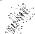
Fig. 1 illustrates the assembly view of a socket interior of example 1; -
Fig. 2 illustrates the exploded view of the socket interior of example 1; -
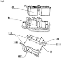
Fig. 3 illustrates the exploded view of a first clapboard and a circuit board of example 1; -
Fig. 4 illustrates the exploded view of a housing and the socket interior of example 1; -
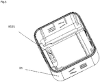
Fig. 5 is the axonometric view of a lower housing in example 1; -
Fig. 6 is the exploded view of a housing and a socket interior of example 2; -
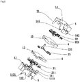
Fig. 7 is the exploded view of a socket interior of example 3; -
Fig. 8 is the exploded view of a socket interior of example 4. - In the drawings:
- 11
- first clapboard;
- 111
- buckle arm;
- 1111
- clamping slot;
- 112
- isolating tendon;
- 1121
- clamping joint;
- 12
- second clapboard;
- 13
- third clapboard;
- 14
- fourth clapboard;
- 141
- clamping projection;
- 142
- first press block;
- 143
- sticking post;
- 21
- live wire plug bush conductive sheet;
- 211
- first wiring pin;
- 22
- naught wire plug bush conductive sheet;
- 221
- second wiring pin;
- 23
- earth wire plug bush conductive sheet;
- 231
- third wiring pin;
- 31
- first positioning post;
- 311
- screwed hole;
- 32
- first positioning hole;
- 33
- counter bore;
- 34
- screw;
- 4
- wiring slot;
- 5
- lead wire limit slot;
- 61
- USB circuit board;
- 62
- heavy-current switch circuit board;
- 63
- insulation board;
- 7
- protective door module;
- 81
- lower housing;
- 811
- bearing surface;
- 812
- jack surface;
- 813
- threading surface;
- 8131
- second press block;
- 8132
- threading hole;
- 82
- upper cover;
- 91
- second positioning post;
- 92
- second positioning hole.
- The disclosure will be described in detail below through examples in combination of the drawings. The following examples are only exemplary and do not limit the protection scope of the present disclosure.
- Please refer to
Fig. 1 andFig. 2 , a 3D convertor comprises a socket interior within a housing. The socket interior comprises clapboards and plug bush conductive sheets. The clapboards include afirst clapboard 11, asecond clapboard 12, athird clapboard 13 and afourth clapboard 14 which are sequentially stacked. While the plug bush conductive sheets comprise a live wire plug bushconductive sheet 21 arranged between thefirst clapboard 11 and thesecond clapboard 12, an earth wire plug bushconductive sheet 23 arranged between thesecond clapboard 12 and thethird clapboard 13, and a naught wire plug bushconductive sheet 22 arranged between thethird clapboard 13 and thefourth clapboard 14. A buckle structure is provided between thefirst clapboard 11 and thefourth clapboard 14 which are at the opposite ends, to form a tight integral socket interior by mutually stacking each clapboard and each plug bush conductive sheet and making them press against each other. The buckle structure may comprise abuckle arm 111 provided at the edge of thefirst clapboard 11 and extending towards thefourth clapboard 14, with aclamping slot 1111 provided on thebuckle arm 111, and a clampingprojection 141 that engages with theclamping slot 1111 of thebuckle arm 111 provided on thefourth clapboard 14. It can be understood that the buckle arm could also be provided on thefourth clapboard 14, while the clampingprojection 141 could be provided on thefirst clapboard 11. And in example 1, in order to make the buckling of the buckle structure more stable, three buckle arms are provided on thefourth clapboard 14 but not in a straight line. The buckle arms respectively surrounds the peripheries of thesecond clapboard 12 and thethird clapboard 13 after the socket interior is assembled; of course, it can be understood that the buckle arms may also buckle with the clampingprojection 141 of thefourth clapboard 14 after respectively passing through thesecond clapboard 12 and thethird clapboard 13. - When installing the plug bush conductive sheets, in order to orientate the installation position between each conductive sheet and each corresponding clapboard more accurately, positioning mechanisms are provided between each conductive sheet and each corresponding clapboard, referring to the visual angle of the clapboards and the conductive sheets in
Fig. 7 .The positioning mechanism comprises second positioning posts 91 provided on a surface of thefirst clapboard 11 facing towards the live wire plug bushconductive sheet 21, on a surface of thesecond clapboard 12 facing towards the earth wire plug bushconductive sheet 23, and on a surface of thethird clapboard 13 facing towards the naught wire plug bushconductive sheet 22; and second positioning holes 92 provided on the live wire plug bushconductive sheet 21, on the earth wire plug bushconductive sheet 23 and on the naught wire plug bushconductive sheet 22 which engage with the second positioning posts 91. The number of the second positioning posts 91 on each clapboard is at least two, so that the conductive sheets can be accurately installed on each clapboard. Of course, it can be understood that the second positioning posts 91 could also be provided on a surface of thefourth clapboard 14 facing towards the naught wire plug bushconductive sheet 22, on a surface of thethird clapboard 13 facing towards the earth wire plug bushconductive sheet 23, and on a surface of thesecond clapboard 12 facing towards the live wire plug bushconductive sheet 21, or simultaneously provided on the opposite two surfaces of corresponding clapboards. - In order to improve the space utilization of the socket interior and the distribution reasonability of conductive wires inside the socket interior, each of the side surfaces of the
second clapboard 12, thethird clapboard 13 and thefourth clapboard 14 which are in the same orientation is recessed inward to form awiring slot 4. And on the side surface of thefourth clapboard 14 there is also provided afirst press block 142 spaning across thewiring slot 4. Referring toFig. 2 , afirst wiring pin 211 is provided on the live wire plug bushconductive sheet 21, and asecond wiring pin 221 is provided on the naught wire plug bushconductive sheet 22. In the assembled socket interior, thefirst wiring pin 211 and thesecond wiring pin 221 are located within thewiring slots 4, leading to the convenience placement of conductive wires such as wiring pins; and athird wiring pin 231 is provided on the earth wire plug bushconductive sheet 23, and thethird wiring pin 231 is bent against the earth wire plug bushconductive sheet 23, and thethird wiring pin 231 passes through thethird clapboard 13 and thefourth clapboard 14 and exposed outside thefourth clapboard 14 after the socket interior is assembled. - As shown in
Fig. 3 , in order to enhance the function of the socket interior, the socket interior is also provided with aUSB circuit board 61 and a heavy-currentswitch circuit board 62. In example 1, a fixed bracket is extended from a surface of thefirst clapboard 11 far away from thesecond clapboard 12 and is configured to lay up the above circuit boards; or a fixed bracket is extended from a surface of thefourth clapboard 14 far away from thethird clapboard 13 and is configured to lay up the above circuit boards. On the surface of thefirst clapboard 11 far away from thesecond clapboard 12 is provided with theUSB circuit board 61 and the heavy-currentswitch circuit board 62, and on this surface of thefirst clapboard 11 is also provided with isolatingtendons 112 configured to insulate the heavy-currentswitch circuit board 62 and theUSB circuit board 61; of course, it can be understood that when theUSB circuit board 61 and the heavy-currentswitch circuit board 62 are provided on the surface of thefourth clapboard 14 far away from thethird clapboard 13, then the isolatingtendons 112 are also correspondingly provided on this surface of thefourth clapboard 14, and meanwhile, thewiring slots 4 are provided on thefirst clapboard 11, thesecond clapboard 12 and thethird clapboard 13, while thefirst press block 142 is provided at the position on thefirst clapboard 11 where it snaps across thewiring slot 4. And in order to make it easier to route the wires, a leadwire limit slot 5 is also provided on the isolatingtendons 112 that corresponds to thepress block 142. -
Fig. 4 is the exploded view of the housing and the socket interior of the 3D convertor. The housing comprises alower housing 81 with an opening and anupper cover 82 that can close the opening. In order to make it easier to install theupper cover 82, let theupper cover 82 correspond to theUSB circuit board 61 and the heavy-currentswitch circuit board 62 of the socket interior, and theupper cover 82 is provided with a USB structure and a switch that turns on/off the 3D convertor. The bottom surface of thelower housing 81 opposing theupper cover 82 is abearing surface 811. Considering the function of the bearingsurface 811, and in order to reduce the volume of the 3D convertor, no jacks are provided on thebearing surface 811. One side surface of thelower housing 81 is provided with a threading hole and defined as a threading surface, and thethreading hole 8132 corresponds to thefirst press block 142, so as to make it easier to lead the wires out from the rocket interior. As shown inFig. 5 , on the inner side of the treadingsurface 813 of thelower housing 81 there is also provided with asecond press block 8131. Thesecond press block 8131 forms as a group with thefirst press block 142 provided on the clapboard. And between thefirst press block 142 and thesecond press block 8131 are formed holes for passing conductive cables, and via this arrangement the quantity of wires inside the socket interior is reduced and the volume of the 3D convertor is also reduced. Other side surfaces of thelower housing 81 are provided with jacks and defined as jack surfaces 812. In order to improve the safety when using the 3D convertor, aprotective door module 7 is provided between the socket interior and thejack surface 812, and to make it easier to install theprotective door module 7, a sticking post 9 is provided on the side surface of the socket interior. Firstly, the sticking post 9 is used to install the socket interior and theprotective door module 7, and then the socket interior installed with theprotective door module 7 is placed into thelower housing 81 as a whole, to make thethreading surface 813 of thelower housing 81 to correspond to thepress block 142 of the socket interior, and successively theupper cover 82 is covered to make a clamping joint 1121 of the socket interior directly plug into a blind hole slot (not shown in the figures) in the inner side of theupper cover 82, and thereby a convenient installation has been completed. It can be understood that, in example 1, said housing may be of other forms. For example, the housing could comprise a middle body with two openings each at its two opposite ends and two end caps each covering one of the two openings of the middle body, that is, thelower housing 81 inFig. 4 is divided into two parts, and for this no further elaboration is needed here. -
Fig. 5 is an exploded view of a housing and a socket interior of a 3D convertor. This 3D convertor differs from that of example 1 in that aninsulation board 63 is provided between thefirst clapboard 11 and the circuit boards, that is, the socket interior is provided with aninsulation board 63 that insulates theUSB circuit board 61 and the heavy-currentswitch circuit board 62 from thefirst clapboard 11. Theinsulation board 63 is configured to increase the electric clearance between the circuit boards and the live wire plug bushconductive sheet 21 or the electric clearance between the circuit boards and the naught wire plug bushconductive sheet 22 to make it comply with the regulations of relevant standards. -
Fig. 6 is the exploded view of the socket interior. The socket interior differs from that of example 1 in that the buckle structure between thefourth clapboard 14 and thefirst clapboard 11 is removed, instead, apositioning post 31 is provided on the surface of thefirst clapboard 11 opposing thesecond clapboard 12, and apositioning hole 32 which engages with thepositioning post 31 is provided on thesecond clapboard 12 and thethird clapboard 13, respectively. A screwedhole 311 which can be locked with a screw is provided on an end surface of thepositioning post 31. And a counter bore 33 is provided on thefourth clapboard 14 that corresponds to the screwedhole 311. It can be understood that thepositioning post 31 may also be provided on the surface of thefourth clapboard 14 opposing the third clapboard 13 (not shown in the figures), and thepositioning hole 32 that engages with thepositioning post 31 is provided on thesecond clapboard 12 and thethird clapboard 13, respectively. The screwedhole 311 which can be locked with thescrew 34 is provided on an end surface of thepositioning post 31, and the counter bore 33 that corresponds to the screwedhole 311 is provided on thefirst clapboard 11. When assembling the socket interior, thepositioning post 31 on thefirst clapboard 11 is allowed to pass through the positioning holes 32 of thesecond clapboard 12 and thethird clapboard 13 in sequence, and then to abut with the counter bore 33 on thefourth clapboard 14. As the end surface of thepositioning post 31 is provided with the screwedhole 311, thescrew 34 can be used to lock into the screwedhole 311, and thereby the fixation and installation of the socket interior are realized. -
Fig. 7 is the exploded view of the socket interior, which differs from example 1 also in the socket interior. In reference to example 1 and example 3, example 4 uses not only the buckle structure but also the structure of thepositioning post 31. Thebuckle arms 111 are provided at the edge of thefirst clapboard 11 and extend towards thefourth clapboard 14. And the buckle arm is provided at each of three corners of thefirst clapboard 11 and the counter bore 33 is provided at the last corner of thefirst clapboard 11. Theclamping slot 1111 is provided on each of thebuckle arms 111, while the clampingprojection 141 that snaps with theclamping slot 1111 of thebuckle arm 111 is provided at each of the corresponding three corners of thefourth clapboard 14, and thepositioning post 31 that corresponds to the counter bore 33 is provided at the last corner of thefourth clapboard 14. It can be understood that the number of thebuckle arm 111 could be one or two, while the number of thepositioning post 31 could be two or three. During installation, each clapboard is superposed over one another, and thescrew 34 is locked into the screwedhole 311 of thepositioning post 31 after thepositioning post 31 corresponds to the counter bore 33, while theclamping slot 1111 of thebuckle arm 111 snaps with the clampingprojection 141, thereby the assembly of the socket interior is finished. It is can be seen that, between each clapboard and its corresponding conductive sheet, no positioning mechanism is provided here. It can be understood that, according to the actual practice, a positioning mechanism as disclosed in example 1 can be provided between each clapboard and its corresponding conductive sheet. - The above are only the preferred examples of the present disclosure. The protection scope of the present disclosure is not limited to the above examples. Any technical solution under the concept of the present disclosure falls within the protection scope of the present disclosure. It should be pointed out that all improvements without deviating from the principles of the present disclosure should be deemed as falling within the protection scope of the disclosure.
Claims (22)
- A three-dimensional convertor, comprising:a housing; and,a socket interior provided inside the housing; wherein,the housing comprises at least two jack surfaces on each of which jacks are provided, each jack corresponds to one of the live wire plug bush conductive sheet (21), the naught wire plug bush conductive sheet (22) and the earth wire plug bush conductive sheet (23).
the socket interior comprises:clapboards comprising a first clapboard (11), a second clapboard (12), a third clapboard (13) and a fourth clapboard (14) which are sequentially stacked; and,a live plug bush conductive sheet (21), a naught wire plug bush conductive sheet (22) and an earth plug bush conductive sheet (23); wherein,the naught wire plug bush conductive sheet (22) is provided between the first clapboard (11) and the second clapboard (12), the earth plug bush conductive sheet (23) is provided between the second clapboard (12) and the third clapboard (13), and the live wire plug bush conductive sheet (21) is provided between the third clapboard (13) and the fourth clapboard (14); - The three-dimensional convertor according to claim 1, wherein, buckle arms which can be buckled with each other is provided between the first clapboard (11) and the fourth clapboard (14), and each clapboard and its corresponding conductive sheet are pressed against each other when the buckle arm of the first clapboard (11) is buckled with that of the fourth clapboard (14).
- The three-dimensional convertor according to claim 2, wherein,
a clamping slot (1111) is provided on the free end of the buckle arm on the first clapboard (11), a clamping projection (141) to buckle with the clamping slot (1111) is provided on the free end of the buckle arm on the fourth clapboard (14); or,
a clamping slot (1111) is provided on the free end of the buckle arm on the fourth clapboard (14), a clamping projection (141) to buckle with the clamping slot (1111) is provided on the free end of the buckle arm on the first clapboard (11). - The three-dimensional convertor according to claim 2, wherein,
the buckle arms surround the peripheries of the second clapboard (12) and the third clapboard (13); or,
the buckle arms passes through the second clapboard (12) and the third clapboard (13). - The three-dimensional convertor according any one of claims 1 to 4, wherein, a first positioning post (31) is provided on the first clapboard (11) or the fourth clapboard (14), and a first positioning hole (32) that engages with the first positioning post (31) is provided on other clapboards except the one provided with the first positioning post (31).
- The three-dimensional convertor according to claim 5, wherein, a threaded hole (311) to lock up with a screw (34) is provided on the free end of the first positioning post (31), and a counter bore (33) to accommodate the screw is provided on the clapboard where the free end of the first positioning post (31) is located.
- The three-dimensional convertor according to claim 1, wherein,
a fixed bracket configured to lay up a circuit board is extended from a surface of the first clapboard (11) far away from the second clapboard (12); or, a fixed bracket configured to lay up a circuit board is extended from a surface of the fourth clapboard (14) far away from the third clapboard (13). - The three-dimensional convertor according to claim 7, wherein, the circuit board comprises a USB circuit board (61) and/or a heavy-current switch circuit board (62), the fixed support comprises isolating tendons (112) configured to insulate the heavy-current switch circuit board (62) and the USB circuit board (61).
- The three-dimensional convertor according to claim 1 or 8, wherein, a threading hole (8132) configured to lead conductive cables out is provided on one side surface of the housing, and a wiring slot (4) is recessed inward in a side surface of the socket interior that corresponds to the threading hole (8132).
- The three-dimensional convertor according to claim 9, wherein, a first wiring pin (211) is provided on the live wire plug bush conductive sheet (21), a second wiring pin (221) is provided on the naught wire plug bush conductive sheet (22), and the first wiring pin (211) and the second wiring pin (221) are both provided in the wiring slot (4).
- The three-dimensional convertor according to claim 9 or 10, wherein, a first press block (142) is provided on a side surface of the socket interior opposing the threading hole (8132), a second press block (8131) is provided under the threading hole (8132) on the inner side of the housing, and the first press block (142) and the second press block (8131) contact with each other when the socket interior is installed in the housing.
- The three-dimensional convertor according to claim 11, wherein, when the first press block (142) and the second press block (8131) contact with each other, a hole configured to let conductive wires pass through the threading hole (8132) is provided between the opposing faces of the first press block (142) and the second press block (8131).
- The three-dimensional convertor according to claim 1, wherein,
a third wiring pin (231) is provided on the earth wire plug bush conductive sheet (23) and is bent and extends towards the fourth clapboard (14), and the third wiring pin (231) penetrates the fourth clapboard (14); or,
a third wiring pin (231) is provided on the earth wire plug bush conductive sheet (23) and is bent and extends towards the first clapboard (14), and the third wiring pin (231) penetrates the first clapboard (11). - The three-dimensional convertor according to claim 9, wherein, the housing comprises a lower housing (81) with an opening and an upper cover (82) that can close the opening, and the threading hole (8132) is provided on a side surface of the lower housing (81).
- The three-dimensional convertor according to claim 14, wherein, the bottom surface of the lower housing (81) opposing the upper cover (82) is a bearing surface (811), and other three side surfaces of the lower housing (81) except the one with the threading hole (8132) are jack surfaces (812), and each of the jack surfaces (812) is provided with a jack.
- The three-dimensional convertor according to claim 1, wherein, a protective door module (7) is provided between the socket interior and the inner side of the housing with the jack, and the protective door module (7) is configured to protect the jack.
- The three-dimensional convertor according to claim 15, wherein, a sticking post (9) is provided on a side surface of the socket interior opposing the inner side of the housing, and the sticking post (9) is configured to orientate the protective door module (7).
- The three-dimensional convertor according to claim 14, wherein, when the socket interior is installed in the housing, the USB circuit board (61) and the heavy-current switch circuit board (62) are provided to oppose the upper cover (82), and a USB interface slot and a switch installation slot are provided on the upper cover (82).
- The three-dimensional convertor according to claim 14, wherein, a clamping joint (1121) is provided on a side of the isolating tendon (112) facing towards the upper cover, the clamping joint (1121) extends towards the upper cover (82), and a blind groove that engages with the clamping joint (1121) is provided on a corresponding inner surface of the upper housing lid (82).
- The three-dimensional convertor according to claim 8, wherein, an insulating board (63) is provided on the first clapboard (11) or the fourth clapboard (14) installed with circuit boards, and the insulating board (63) is configured to insulate the USB circuit board (61) and the heavy-current switch circuit board (62).
- The three-dimensional convertor according to claim 1, wherein, a positioning mechanism is provided between each clapboard and each corresponding conductive sheet which are stacked alternatively, and the positioning mechanism is configured to orientate each conductive sheet to each corresponding clapboard.
- The three-dimensional convertor according to claim 21, wherein, the positioning mechanism comprises a second positioning post (91) provided on the clapboard, and a second positioning hole (92) respectively provided on the live wire plug bush conductive sheet (21), the naught wire plug bush conductive sheet (22) and the earth wire plug bush conductive sheet (23), second positioning holes (92) are one to one corresponding to and engage with second positioning posts (91).
Applications Claiming Priority (2)
| Application Number | Priority Date | Filing Date | Title |
|---|---|---|---|
| CN201620043644.3U CN205355372U (en) | 2016-01-18 | 2016-01-18 | Multi -face jack |
| PCT/CN2017/076997 WO2017125095A1 (en) | 2016-01-18 | 2017-03-16 | Three-dimensional converter |
Publications (3)
| Publication Number | Publication Date |
|---|---|
| EP3379656A1 true EP3379656A1 (en) | 2018-09-26 |
| EP3379656A4 EP3379656A4 (en) | 2019-07-10 |
| EP3379656B1 EP3379656B1 (en) | 2022-09-21 |
Family
ID=56176561
Family Applications (1)
| Application Number | Title | Priority Date | Filing Date |
|---|---|---|---|
| EP17741126.1A Active EP3379656B1 (en) | 2016-01-18 | 2017-03-16 | Three-dimensional converter |
Country Status (5)
| Country | Link |
|---|---|
| US (1) | US10601192B2 (en) |
| EP (1) | EP3379656B1 (en) |
| JP (1) | JP2019517706A (en) |
| CN (1) | CN205355372U (en) |
| WO (1) | WO2017125095A1 (en) |
Cited By (1)
| Publication number | Priority date | Publication date | Assignee | Title |
|---|---|---|---|---|
| NL2021785B1 (en) * | 2018-10-09 | 2020-05-13 | Designnest B V | Power outlet device |
Families Citing this family (8)
| Publication number | Priority date | Publication date | Assignee | Title |
|---|---|---|---|---|
| CN205355372U (en) * | 2016-01-18 | 2016-06-29 | 公牛集团有限公司 | Multi -face jack |
| CN106129696B (en) * | 2016-08-10 | 2019-08-13 | 杭州鸿雁电器有限公司 | A kind of modularization intelligent socket and its assemble method |
| CN108232680B (en) * | 2018-04-07 | 2023-09-22 | 佛山市顺德区信辉达电子有限公司 | Relay rack for leakage protection plug |
| CN208284696U (en) * | 2018-06-01 | 2018-12-25 | 深圳市联讯发科技有限公司 | A kind of integral type Three-dimensional socket |
| CN109004424A (en) * | 2018-08-02 | 2018-12-14 | 上海飞科电器股份有限公司 | Magic square Multi-face socket |
| CN109742575B (en) * | 2019-01-17 | 2024-02-27 | 深圳市航嘉驰源电气股份有限公司 | Square socket |
| CN109755790B (en) * | 2019-03-20 | 2023-09-12 | 宁波奥博尔电器有限公司 | Multi-face three-dimensional lock pin and spherical socket with same |
| CN215119337U (en) * | 2021-05-06 | 2021-12-10 | 黄志福 | Terminal integrated safety socket |
Family Cites Families (19)
| Publication number | Priority date | Publication date | Assignee | Title |
|---|---|---|---|---|
| US4313646A (en) * | 1980-02-25 | 1982-02-02 | Amp Incorporated | Power distribution system |
| US5094630A (en) * | 1991-02-25 | 1992-03-10 | Jammet Jean Claude | Multiple socket attachment |
| US5281172A (en) * | 1992-12-04 | 1994-01-25 | Pacomex Industries, Inc. | Electrical outlet adapter |
| US5383799A (en) * | 1993-03-26 | 1995-01-24 | Fladung; Philip E. | Multi-purpose plug-in electrical outlet adaptor |
| US6015303A (en) * | 1997-10-17 | 2000-01-18 | Hubbell Incorporated | Electrical receptacle assembly with multiple sites of dual snap-fit securement means |
| US6488540B2 (en) * | 2000-09-08 | 2002-12-03 | Heyco, Inc. | Multi-receptacle electrical outlet |
| US6929514B1 (en) * | 2004-05-17 | 2005-08-16 | Chao Da Trading Co., Ltd. | Socket with non-connecting terminal |
| US20060216986A1 (en) | 2005-03-25 | 2006-09-28 | Abbas Amiri-Hezaveh | Compact signal distribution device |
| US7892036B2 (en) * | 2008-12-30 | 2011-02-22 | Multiway Industries (Hk) Ltd. | Electrical wall tap assembly |
| CN201629446U (en) | 2010-02-11 | 2010-11-10 | 黄浩波 | Multifunctional superposable socket |
| CN203721952U (en) * | 2013-12-16 | 2014-07-16 | 苏州波特利五金照明电器有限公司 | Internal structure of square socket |
| CN203787656U (en) | 2013-12-30 | 2014-08-20 | 慈溪市清风电子有限公司 | Vertical type socket |
| US9306349B2 (en) | 2014-01-21 | 2016-04-05 | Allocacoc Corporation | Construction of an alternating current (AC) power socket |
| JP2015138691A (en) * | 2014-01-23 | 2015-07-30 | 株式会社Cjプライムショッピング | Table tap |
| CN204304180U (en) * | 2014-11-05 | 2015-04-29 | 慈溪市清风电子有限公司 | A kind of magic cube socket |
| CN204349054U (en) * | 2014-12-30 | 2015-05-20 | 国光电器股份有限公司 | A kind of three-dimensional Multi-face socket unit and plate connector |
| CN204966859U (en) | 2015-08-25 | 2016-01-13 | 广东顺科通信设备实业有限公司 | Reverse opening shielding is pressed from both sides |
| CN105207020A (en) | 2015-09-28 | 2015-12-30 | 洛阳德威机电科技有限公司 | Magic cube type combined socket and method thereof |
| CN205355372U (en) * | 2016-01-18 | 2016-06-29 | 公牛集团有限公司 | Multi -face jack |
-
2016
- 2016-01-18 CN CN201620043644.3U patent/CN205355372U/en active Active
-
2017
- 2017-03-16 WO PCT/CN2017/076997 patent/WO2017125095A1/en active Application Filing
- 2017-03-16 JP JP2018538619A patent/JP2019517706A/en active Pending
- 2017-03-16 EP EP17741126.1A patent/EP3379656B1/en active Active
- 2017-03-16 US US16/064,985 patent/US10601192B2/en active Active
Cited By (1)
| Publication number | Priority date | Publication date | Assignee | Title |
|---|---|---|---|---|
| NL2021785B1 (en) * | 2018-10-09 | 2020-05-13 | Designnest B V | Power outlet device |
Also Published As
| Publication number | Publication date |
|---|---|
| EP3379656B1 (en) | 2022-09-21 |
| US20180323558A1 (en) | 2018-11-08 |
| WO2017125095A1 (en) | 2017-07-27 |
| JP2019517706A (en) | 2019-06-24 |
| EP3379656A4 (en) | 2019-07-10 |
| US10601192B2 (en) | 2020-03-24 |
| CN205355372U (en) | 2016-06-29 |
Similar Documents
| Publication | Publication Date | Title |
|---|---|---|
| US10601192B2 (en) | Three-dimensional convertor | |
| CN103116051B (en) | Pluggable electric meter box | |
| EP2584615A1 (en) | Combiner box | |
| JP2007195319A (en) | Electrical connection box | |
| CN102362374A (en) | Bus bar device and fusible link unit | |
| CN108551138B (en) | Be applied to copper bar clamping device of generating line | |
| CN207818929U (en) | Terminal box | |
| CN203164245U (en) | Plug-type electric meter box | |
| CN204376000U (en) | A kind of terminal cap of controller and controller | |
| CN202797317U (en) | Connection terminal | |
| CN219040756U (en) | Socket | |
| CN205407169U (en) | Split type terminal box for electric motor car | |
| CN208127444U (en) | The mounting structure of connecting terminal | |
| CN211605435U (en) | Wiring terminal | |
| CN201616538U (en) | Cable combination body and cable connector applied by cable combination body | |
| CN204230513U (en) | Electrical micro-machine connector and the connector assembly with this electrical micro-machine connector | |
| CN207781427U (en) | Manual maintenance switchs | |
| CN213460140U (en) | Through-wall type wiring terminal and low-voltage switch cabinet with same | |
| CN217788921U (en) | A kind of interface unit | |
| CN214204018U (en) | Rotatable binding post row | |
| CN213602238U (en) | Outdoor cabinet | |
| CN212935153U (en) | Outdoor wiring cabinet | |
| CN219998576U (en) | Plug-in wiring terminal | |
| CN218783253U (en) | Participate in, panel structure and row of inserting thereof | |
| CN215911984U (en) | Motor housing with wire outlet waterproof structure |
Legal Events
| Date | Code | Title | Description |
|---|---|---|---|
| STAA | Information on the status of an ep patent application or granted ep patent |
Free format text: STATUS: THE INTERNATIONAL PUBLICATION HAS BEEN MADE |
|
| PUAI | Public reference made under article 153(3) epc to a published international application that has entered the european phase |
Free format text: ORIGINAL CODE: 0009012 |
|
| STAA | Information on the status of an ep patent application or granted ep patent |
Free format text: STATUS: REQUEST FOR EXAMINATION WAS MADE |
|
| 17P | Request for examination filed |
Effective date: 20180621 |
|
| AK | Designated contracting states |
Kind code of ref document: A1 Designated state(s): AL AT BE BG CH CY CZ DE DK EE ES FI FR GB GR HR HU IE IS IT LI LT LU LV MC MK MT NL NO PL PT RO RS SE SI SK SM TR |
|
| AX | Request for extension of the european patent |
Extension state: BA ME |
|
| XX | Miscellaneous (additional remarks) |
Free format text: A REQUEST FOR RESTORATION OF THE RIGHT OF PRIORITY BY THE EPO AS DESIGNATED OFFICE HAS BEEN GRANTED (R. 49TER.2 PCT, ART.122 EPC). |
|
| RIN1 | Information on inventor provided before grant (corrected) |
Inventor name: ZHANG, JIALU Inventor name: WANG, HUIJIU Inventor name: YAN, LEI Inventor name: DENG, HAO |
|
| DAV | Request for validation of the european patent (deleted) | ||
| DAX | Request for extension of the european patent (deleted) | ||
| REG | Reference to a national code |
Ref country code: DE Ref legal event code: R079 Ref document number: 602017061964 Country of ref document: DE Free format text: PREVIOUS MAIN CLASS: H01R0013514000 Ipc: H01R0024220000 |
|
| A4 | Supplementary search report drawn up and despatched |
Effective date: 20190606 |
|
| RIC1 | Information provided on ipc code assigned before grant |
Ipc: H01R 25/00 20060101ALI20190531BHEP Ipc: H01R 13/46 20060101ALI20190531BHEP Ipc: H01R 24/22 20110101AFI20190531BHEP Ipc: H01R 31/02 20060101ALI20190531BHEP Ipc: H01R 13/506 20060101ALI20190531BHEP Ipc: H01R 13/514 20060101ALI20190531BHEP |
|
| STAA | Information on the status of an ep patent application or granted ep patent |
Free format text: STATUS: EXAMINATION IS IN PROGRESS |
|
| STAA | Information on the status of an ep patent application or granted ep patent |
Free format text: STATUS: EXAMINATION IS IN PROGRESS |
|
| 17Q | First examination report despatched |
Effective date: 20201218 |
|
| STAA | Information on the status of an ep patent application or granted ep patent |
Free format text: STATUS: EXAMINATION IS IN PROGRESS |
|
| GRAP | Despatch of communication of intention to grant a patent |
Free format text: ORIGINAL CODE: EPIDOSNIGR1 |
|
| STAA | Information on the status of an ep patent application or granted ep patent |
Free format text: STATUS: GRANT OF PATENT IS INTENDED |
|
| INTG | Intention to grant announced |
Effective date: 20220420 |
|
| INTG | Intention to grant announced |
Effective date: 20220420 |
|
| GRAS | Grant fee paid |
Free format text: ORIGINAL CODE: EPIDOSNIGR3 |
|
| GRAA | (expected) grant |
Free format text: ORIGINAL CODE: 0009210 |
|
| STAA | Information on the status of an ep patent application or granted ep patent |
Free format text: STATUS: THE PATENT HAS BEEN GRANTED |
|
| AK | Designated contracting states |
Kind code of ref document: B1 Designated state(s): AL AT BE BG CH CY CZ DE DK EE ES FI FR GB GR HR HU IE IS IT LI LT LU LV MC MK MT NL NO PL PT RO RS SE SI SK SM TR |
|
| REG | Reference to a national code |
Ref country code: GB Ref legal event code: FG4D |
|
| XX | Miscellaneous (additional remarks) |
Free format text: A REQUEST FOR RESTORATION OF THE RIGHT OF PRIORITY BY THE EPO AS DESIGNATED OFFICE HAS BEEN GRANTED (R. 49TER.2 PCT, ART.122 EPC). |
|
| REG | Reference to a national code |
Ref country code: CH Ref legal event code: EP |
|
| REG | Reference to a national code |
Ref country code: IE Ref legal event code: FG4D |
|
| REG | Reference to a national code |
Ref country code: DE Ref legal event code: R096 Ref document number: 602017061964 Country of ref document: DE |
|
| REG | Reference to a national code |
Ref country code: AT Ref legal event code: REF Ref document number: 1520436 Country of ref document: AT Kind code of ref document: T Effective date: 20221015 |
|
| REG | Reference to a national code |
Ref country code: LT Ref legal event code: MG9D |
|
| REG | Reference to a national code |
Ref country code: NL Ref legal event code: MP Effective date: 20220921 |
|
| PG25 | Lapsed in a contracting state [announced via postgrant information from national office to epo] |
Ref country code: SE Free format text: LAPSE BECAUSE OF FAILURE TO SUBMIT A TRANSLATION OF THE DESCRIPTION OR TO PAY THE FEE WITHIN THE PRESCRIBED TIME-LIMIT Effective date: 20220921 Ref country code: RS Free format text: LAPSE BECAUSE OF FAILURE TO SUBMIT A TRANSLATION OF THE DESCRIPTION OR TO PAY THE FEE WITHIN THE PRESCRIBED TIME-LIMIT Effective date: 20220921 Ref country code: NO Free format text: LAPSE BECAUSE OF FAILURE TO SUBMIT A TRANSLATION OF THE DESCRIPTION OR TO PAY THE FEE WITHIN THE PRESCRIBED TIME-LIMIT Effective date: 20221221 Ref country code: LV Free format text: LAPSE BECAUSE OF FAILURE TO SUBMIT A TRANSLATION OF THE DESCRIPTION OR TO PAY THE FEE WITHIN THE PRESCRIBED TIME-LIMIT Effective date: 20220921 Ref country code: LT Free format text: LAPSE BECAUSE OF FAILURE TO SUBMIT A TRANSLATION OF THE DESCRIPTION OR TO PAY THE FEE WITHIN THE PRESCRIBED TIME-LIMIT Effective date: 20220921 Ref country code: FI Free format text: LAPSE BECAUSE OF FAILURE TO SUBMIT A TRANSLATION OF THE DESCRIPTION OR TO PAY THE FEE WITHIN THE PRESCRIBED TIME-LIMIT Effective date: 20220921 |
|
| REG | Reference to a national code |
Ref country code: AT Ref legal event code: MK05 Ref document number: 1520436 Country of ref document: AT Kind code of ref document: T Effective date: 20220921 |
|
| PG25 | Lapsed in a contracting state [announced via postgrant information from national office to epo] |
Ref country code: HR Free format text: LAPSE BECAUSE OF FAILURE TO SUBMIT A TRANSLATION OF THE DESCRIPTION OR TO PAY THE FEE WITHIN THE PRESCRIBED TIME-LIMIT Effective date: 20220921 Ref country code: GR Free format text: LAPSE BECAUSE OF FAILURE TO SUBMIT A TRANSLATION OF THE DESCRIPTION OR TO PAY THE FEE WITHIN THE PRESCRIBED TIME-LIMIT Effective date: 20221222 |
|
| PG25 | Lapsed in a contracting state [announced via postgrant information from national office to epo] |
Ref country code: SM Free format text: LAPSE BECAUSE OF FAILURE TO SUBMIT A TRANSLATION OF THE DESCRIPTION OR TO PAY THE FEE WITHIN THE PRESCRIBED TIME-LIMIT Effective date: 20220921 Ref country code: RO Free format text: LAPSE BECAUSE OF FAILURE TO SUBMIT A TRANSLATION OF THE DESCRIPTION OR TO PAY THE FEE WITHIN THE PRESCRIBED TIME-LIMIT Effective date: 20220921 Ref country code: PT Free format text: LAPSE BECAUSE OF FAILURE TO SUBMIT A TRANSLATION OF THE DESCRIPTION OR TO PAY THE FEE WITHIN THE PRESCRIBED TIME-LIMIT Effective date: 20230123 Ref country code: ES Free format text: LAPSE BECAUSE OF FAILURE TO SUBMIT A TRANSLATION OF THE DESCRIPTION OR TO PAY THE FEE WITHIN THE PRESCRIBED TIME-LIMIT Effective date: 20220921 Ref country code: CZ Free format text: LAPSE BECAUSE OF FAILURE TO SUBMIT A TRANSLATION OF THE DESCRIPTION OR TO PAY THE FEE WITHIN THE PRESCRIBED TIME-LIMIT Effective date: 20220921 Ref country code: AT Free format text: LAPSE BECAUSE OF FAILURE TO SUBMIT A TRANSLATION OF THE DESCRIPTION OR TO PAY THE FEE WITHIN THE PRESCRIBED TIME-LIMIT Effective date: 20220921 |
|
| PGFP | Annual fee paid to national office [announced via postgrant information from national office to epo] |
Ref country code: FR Payment date: 20230327 Year of fee payment: 7 |
|
| PG25 | Lapsed in a contracting state [announced via postgrant information from national office to epo] |
Ref country code: SK Free format text: LAPSE BECAUSE OF FAILURE TO SUBMIT A TRANSLATION OF THE DESCRIPTION OR TO PAY THE FEE WITHIN THE PRESCRIBED TIME-LIMIT Effective date: 20220921 Ref country code: PL Free format text: LAPSE BECAUSE OF FAILURE TO SUBMIT A TRANSLATION OF THE DESCRIPTION OR TO PAY THE FEE WITHIN THE PRESCRIBED TIME-LIMIT Effective date: 20220921 Ref country code: IS Free format text: LAPSE BECAUSE OF FAILURE TO SUBMIT A TRANSLATION OF THE DESCRIPTION OR TO PAY THE FEE WITHIN THE PRESCRIBED TIME-LIMIT Effective date: 20230121 Ref country code: EE Free format text: LAPSE BECAUSE OF FAILURE TO SUBMIT A TRANSLATION OF THE DESCRIPTION OR TO PAY THE FEE WITHIN THE PRESCRIBED TIME-LIMIT Effective date: 20220921 |
|
| PGFP | Annual fee paid to national office [announced via postgrant information from national office to epo] |
Ref country code: DE Payment date: 20230321 Year of fee payment: 7 |
|
| REG | Reference to a national code |
Ref country code: DE Ref legal event code: R097 Ref document number: 602017061964 Country of ref document: DE |
|
| PG25 | Lapsed in a contracting state [announced via postgrant information from national office to epo] |
Ref country code: NL Free format text: LAPSE BECAUSE OF FAILURE TO SUBMIT A TRANSLATION OF THE DESCRIPTION OR TO PAY THE FEE WITHIN THE PRESCRIBED TIME-LIMIT Effective date: 20220921 Ref country code: AL Free format text: LAPSE BECAUSE OF FAILURE TO SUBMIT A TRANSLATION OF THE DESCRIPTION OR TO PAY THE FEE WITHIN THE PRESCRIBED TIME-LIMIT Effective date: 20220921 |
|
| PLBE | No opposition filed within time limit |
Free format text: ORIGINAL CODE: 0009261 |
|
| STAA | Information on the status of an ep patent application or granted ep patent |
Free format text: STATUS: NO OPPOSITION FILED WITHIN TIME LIMIT |
|
| PG25 | Lapsed in a contracting state [announced via postgrant information from national office to epo] |
Ref country code: DK Free format text: LAPSE BECAUSE OF FAILURE TO SUBMIT A TRANSLATION OF THE DESCRIPTION OR TO PAY THE FEE WITHIN THE PRESCRIBED TIME-LIMIT Effective date: 20220921 |
|
| 26N | No opposition filed |
Effective date: 20230622 |
|
| PG25 | Lapsed in a contracting state [announced via postgrant information from national office to epo] |
Ref country code: SI Free format text: LAPSE BECAUSE OF FAILURE TO SUBMIT A TRANSLATION OF THE DESCRIPTION OR TO PAY THE FEE WITHIN THE PRESCRIBED TIME-LIMIT Effective date: 20220921 |
|
| PG25 | Lapsed in a contracting state [announced via postgrant information from national office to epo] |
Ref country code: MC Free format text: LAPSE BECAUSE OF FAILURE TO SUBMIT A TRANSLATION OF THE DESCRIPTION OR TO PAY THE FEE WITHIN THE PRESCRIBED TIME-LIMIT Effective date: 20220921 |
|
| REG | Reference to a national code |
Ref country code: CH Ref legal event code: PL |
|
| GBPC | Gb: european patent ceased through non-payment of renewal fee |
Effective date: 20230316 |
|
| REG | Reference to a national code |
Ref country code: BE Ref legal event code: MM Effective date: 20230331 |
|
| PG25 | Lapsed in a contracting state [announced via postgrant information from national office to epo] |
Ref country code: LU Free format text: LAPSE BECAUSE OF NON-PAYMENT OF DUE FEES Effective date: 20230316 |
|
| REG | Reference to a national code |
Ref country code: IE Ref legal event code: MM4A |
|
| PG25 | Lapsed in a contracting state [announced via postgrant information from national office to epo] |
Ref country code: GB Free format text: LAPSE BECAUSE OF NON-PAYMENT OF DUE FEES Effective date: 20230316 |
|
| PG25 | Lapsed in a contracting state [announced via postgrant information from national office to epo] |
Ref country code: LI Free format text: LAPSE BECAUSE OF NON-PAYMENT OF DUE FEES Effective date: 20230331 Ref country code: IE Free format text: LAPSE BECAUSE OF NON-PAYMENT OF DUE FEES Effective date: 20230316 Ref country code: GB Free format text: LAPSE BECAUSE OF NON-PAYMENT OF DUE FEES Effective date: 20230316 Ref country code: CH Free format text: LAPSE BECAUSE OF NON-PAYMENT OF DUE FEES Effective date: 20230331 |
|
| PG25 | Lapsed in a contracting state [announced via postgrant information from national office to epo] |
Ref country code: BE Free format text: LAPSE BECAUSE OF NON-PAYMENT OF DUE FEES Effective date: 20230331 |