EP3379274A1 - Multi-level logic analyzer for analyzing multi-level digital signals and method for operating a multi-level logic analyzer for analyzing multi-level digital signals - Google Patents
Multi-level logic analyzer for analyzing multi-level digital signals and method for operating a multi-level logic analyzer for analyzing multi-level digital signals Download PDFInfo
- Publication number
- EP3379274A1 EP3379274A1 EP17162481.0A EP17162481A EP3379274A1 EP 3379274 A1 EP3379274 A1 EP 3379274A1 EP 17162481 A EP17162481 A EP 17162481A EP 3379274 A1 EP3379274 A1 EP 3379274A1
- Authority
- EP
- European Patent Office
- Prior art keywords
- signal
- level
- input
- comparison units
- logic analyzer
- Prior art date
- Legal status (The legal status is an assumption and is not a legal conclusion. Google has not performed a legal analysis and makes no representation as to the accuracy of the status listed.)
- Granted
Links
Images



Classifications
-
- G—PHYSICS
- G01—MEASURING; TESTING
- G01R—MEASURING ELECTRIC VARIABLES; MEASURING MAGNETIC VARIABLES
- G01R29/00—Arrangements for measuring or indicating electric quantities not covered by groups G01R19/00 - G01R27/00
- G01R29/02—Measuring characteristics of individual pulses, e.g. deviation from pulse flatness, rise time or duration
-
- G—PHYSICS
- G01—MEASURING; TESTING
- G01R—MEASURING ELECTRIC VARIABLES; MEASURING MAGNETIC VARIABLES
- G01R31/00—Arrangements for testing electric properties; Arrangements for locating electric faults; Arrangements for electrical testing characterised by what is being tested not provided for elsewhere
-
- G—PHYSICS
- G01—MEASURING; TESTING
- G01R—MEASURING ELECTRIC VARIABLES; MEASURING MAGNETIC VARIABLES
- G01R13/00—Arrangements for displaying electric variables or waveforms
- G01R13/02—Arrangements for displaying electric variables or waveforms for displaying measured electric variables in digital form
- G01R13/0218—Circuits therefor
- G01R13/0272—Circuits therefor for sampling
-
- G—PHYSICS
- G01—MEASURING; TESTING
- G01R—MEASURING ELECTRIC VARIABLES; MEASURING MAGNETIC VARIABLES
- G01R13/00—Arrangements for displaying electric variables or waveforms
- G01R13/02—Arrangements for displaying electric variables or waveforms for displaying measured electric variables in digital form
- G01R13/0218—Circuits therefor
- G01R13/0236—Circuits therefor for presentation of more than one variable
-
- G—PHYSICS
- G01—MEASURING; TESTING
- G01R—MEASURING ELECTRIC VARIABLES; MEASURING MAGNETIC VARIABLES
- G01R31/00—Arrangements for testing electric properties; Arrangements for locating electric faults; Arrangements for electrical testing characterised by what is being tested not provided for elsewhere
- G01R31/28—Testing of electronic circuits, e.g. by signal tracer
- G01R31/317—Testing of digital circuits
- G01R31/3177—Testing of logic operation, e.g. by logic analysers
-
- H—ELECTRICITY
- H04—ELECTRIC COMMUNICATION TECHNIQUE
- H04L—TRANSMISSION OF DIGITAL INFORMATION, e.g. TELEGRAPHIC COMMUNICATION
- H04L25/00—Baseband systems
- H04L25/38—Synchronous or start-stop systems, e.g. for Baudot code
- H04L25/40—Transmitting circuits; Receiving circuits
- H04L25/49—Transmitting circuits; Receiving circuits using code conversion at the transmitter; using predistortion; using insertion of idle bits for obtaining a desired frequency spectrum; using three or more amplitude levels ; Baseband coding techniques specific to data transmission systems
- H04L25/4917—Transmitting circuits; Receiving circuits using code conversion at the transmitter; using predistortion; using insertion of idle bits for obtaining a desired frequency spectrum; using three or more amplitude levels ; Baseband coding techniques specific to data transmission systems using multilevel codes
Definitions
- the present invention relates to a multi-level logic analyzer for analyzing multi-level digital signals.
- the present invention further relates to a method for operating a multi-level logic analyzer.
- oscilloscopes maybe used to record analogue voltage and/or current values.
- some oscilloscopes or logic analyzers allow recording logic values, where the logic state, i.e. true/false, 1/0 or on/off, is recorded. Such logic values only show the logical content of the signals but cannot represent the waveform any more.
- a device under test uses multi-level signals, like e.g. PAM3 signals with three logic states, these signals may e.g. be recorded with an analogue input of an oscilloscope and the user may manually evaluate the different signal levels or provide the recorded signal levels from the oscilloscope e.g. to a computer to perform an automated evaluation.
- the oscilloscope may also provide a multi-level signal evaluation after recording the signal via an analogue input or channel.
- the problem addressed by the present invention is providing an improved measurement of multi-level signals.
- the present invention solves this object by a multi-level logic analyzer with the features of claim 1, and by a method for operating a multi-level logic analyzer with the features of claim 10.
- the present invention provides a multi-level logic analyzer with a plurality of signal inputs. Plurality in this context may refer to any number larger than one. Further, the multi-level logic analyzer provides a plurality of comparison units that compare two signals at their inputs.
- first switching means may couple the single signal inputs each with at least two of the comparison units.
- This arrangement of the multi-level logic analyzer allows analyzing multi-level signals without the need to use e.g. an analogue channel of an oscilloscope.
- the number of analogue channels on an oscilloscope is usually limited, e.g. to four.
- these analogue channels may be reserved for analogue measurements and the multi-level signals may be measured via the multi-level logic analyzer that may e.g. be integrated into an oscilloscope or the like.
- the first switching means may e.g. couple a single signal input to as many comparison units as the signal has logic levels or signal levels. If for example a signal is a PAM3 signal with three logic levels, the respective signal input may be coupled to two of the comparison units. Only two of the comparison units are needed, since one of the signal levels is the zero level.
- the two comparison units may then e.g. have different switching levels that represent the logic levels of the input signal. If the logic level of the input signal is the first or lowest logic level, none of the comparison units will output a signal or they will output a zero or low signal. If the logic level of the input signal is the second level, only the first of the comparison units will output a positive signal. If the logic level of the input signal is the third level, both of the comparison units will output a positive signal.
- the output of the comparison units may then further be processed to evaluate the number of positive outputs and determine the signal level of the multi-level signal.
- the comparison units may e.g. be comparators or subtractors and the first comparator inputs may be the positive inputs of the comparators or subtractors, and the second comparator inputs may be the negative inputs of the comparators or subtractors. This will lead to an inverse output.
- the signal inputs may also be switched. This will provide a normal or noninverted output.
- the multi-level logic analyzer may comprise a plurality, i.e. two or more, of signal outputs, each signal output being configured to output an output signal.
- the signal outputs may provide the output signals to following signal processing units.
- the signal outputs may perform any kind of signal conditioning.
- the signal outputs may output any kind of signal, like e.g. an analogue or a digital serial or parallel signal.
- the multi-level logic analyzer may comprise second switching means configured to controllably couple comparison units that are coupled on their first comparison input with the same signal input on their output side with one of the signal outputs.
- comparison units are coupled to a single signal input, they may each serve to analyze a different level of the multi-level logic signal that is provided as input signal to the respective signal input. Coupling all of these comparison units to a single output allows providing a following signal processing unit with a single signal that represents the different signal levels of the multi-level input signal.
- the signal outputs may comprise an encoder that is configured to encode output signals of the comparison units that are connected to the respective signal output into binary values or serialize the output signals of the respective comparison units.
- the number of comparison units that show a positive or high value represents the momentary level present at the multi-level input signal. Therefore, encoding this number into a binary value or a serial digital signal allows providing the following signal processing unit with an indication of the momentary level of the multi-level input signal that is easily usable in digital systems.
- the second switching means may further be configured to controllably couple comparison units that are coupled on their input side with a single signal input on their output side with different signal outputs.
- the multi-level logic analyzer may comprise a plurality, i.e. two or more, of configurable threshold voltage sources, each threshold voltage source being configured to provide a configured output voltage.
- the configurable threshold voltage sources may serve in the multi-level logic analyzer to provide the comparison units with respective threshold voltages as a basis for performing the comparison of the multi-level input signal to determine the momentary level of the multi-level input signal. This means that the comparison units will compare the respective threshold voltage with the input signal provided to the respective comparison unit.
- the multi-level logic analyzer may comprise a plurality, i.e. two or more, of third switching means being configured to couple one of the threshold voltage sources with at least two of the comparison units, especially when the respective two of the comparison units are coupled to different signal inputs.
- two of the comparison units are provided with the same threshold voltage, their output will be triggered by the same signal levels on the input sides. Therefore, two different input signals at two different signal inputs may be compared with the same threshold voltage.
- the threshold voltage sources may be configured to each output a different threshold voltage.
- the threshold voltage sources are configurable, it is possible to configure each one of the threshold voltage sources according to a predetermined signal level of the received multi-level signal.
- two of the threshold voltage sources may be configured to provide threshold voltages, which are in the middle of the voltage range between the respective voltage levels of the multi-level signal.
- a first threshold voltage source could be configured to provide 1,25 V
- a second threshold voltage source could be configured to provide 3,75 V.
- the first switching means may further be configured to couple one of the signal inputs with a first comparator input of one of the comparison units and one of the signal inputs with the second comparator input of the respective comparison unit.
- Fig. 1 shows a block diagram of a multi-level logic analyzer 100 for analyzing multi-level digital signals 101, 102.
- the multi-level digital signals 101, 102 shown in Fig. 1 just exemplarily comprise three voltage levels. It is however understood that the present invention may be applied to multi-level digital signals with any number of signal levels.
- the multi-level logic analyzer 100 comprises a plurality of signal inputs, wherein only two signal inputs 103, 104 are shown and further signal inputs are hinted at by three dots.
- the multi-level logic analyzer 100 further comprises for every one of the signal inputs 103, 104 a first switching means 113, 114. As with the signal inputs 103, 104 only two first switching means 113, 114 are shown and further first switching means are hinted at by three dots.
- the multi-level logic analyzer 100 comprises a plurality of comparison units 105, 106, wherein only two are shown and further comparison units are hinted at by three dots.
- the comparison units 105, 106 are coupled to respective signal outputs 115, 116 to provide their comparator outputs 111, 112 e.g. to a following signal processing unit (not shown).
- the first switching means 113, 114 each receive one of the multi-level digital signals 101, 102.
- the first switching means 113, 114 may then forward the multi-level digital signals 101, 102 to at least two of the comparison units 105, 106, depending on the number of signal levels of the multi-level digital signals 101, 102.
- the first switching means 113, 114 will especially forward the multi-level digital signals 101, 102 to as many comparison units 105, 106 as are needed to process all signal levels of the multi-level digital signals 101, 102, e.g. one less than the number of signal levels.
- the first switching means 113 may forward the multi-level digital signal 101 to the two shown first switching means 113, 114.
- the first switching means 114 may forward the multi-level digital signal 102 to two further not shown comparison units. This allows the multi-level logic analyzer 100 to process multiple multi-level digital signals 101, 102 at the same time with simple switches and comparators.
- the comparison units 105, 106 may receive the multi-level digital signal 101 via a first comparator input 107, 108.
- a comparison voltage selected according to the signal levels of the multi-level digital signal 101 may be provided on the second comparator inputs 109, 110.
- the comparison units 105, 106 may e.g. provide a positive output, if the signal level on the first comparator input 107, 108 is higher than the signal level on the second comparator input 109, 110.
- the comparison voltage of the first switching means 113 may e.g. be between the first and the second signal level of the multi-level digital signal 101
- the comparison voltage of the first switching means 114 may e.g. be between the second and the third signal level of the multi-level digital signal 101.
- both comparison units 105, 106 provide a negative or low signal, when the multi-level digital signal 101 has the first signal level.
- the comparison unit 105 will provide a positive output, when the multi-level digital signal 101 has the second signal level, and both comparison units 105, 106 will provide a positive output signal, when the multi-level digital signal 101 has the third signal level.
- the above may be applied to any number of multi-level digital signals 101, 102 and any number of signal levels.
- the first switching means 113, 114 may e.g. be provided with a number of switching elements that is as high as the maximum number of signal levels that have to be analyzed.
- the first switching means 113, 114 may e.g. be combined into a switching matrix that may comprise any number of switches, like e.g. digitally controllable switches. It is further understood, that the multi-level logic analyzer 100 may comprise any further elements, like e.g. filters, amplifier, and attenuators that are necessary to receive or output the multi-level digital signals 101, 102 or the comparator output signals 111, 112. In addition, the multi-level logic analyzer 100 may comprise a control unit that configures the first switching means 113, 114 and any other configurable element of the multi-level logic analyzer 100 e.g. based on test parameters or a user input.
- a control unit that configures the first switching means 113, 114 and any other configurable element of the multi-level logic analyzer 100 e.g. based on test parameters or a user input.
- Fig. 2 shows a block diagram of another multi-level logic analyzer 200.
- the multi-level logic analyzer 200 is based on the multi-level logic analyzer 100 and therefore also comprises signal inputs 203, 204, first switching means 213, 214, comparison units 205, 206, and the signal outputs 215, 216.
- the above description also applies to these elements of the multi-level logic analyzer 200.
- the multi-level logic analyzer 200 comprises second switching means 217 that are coupled between the comparison units 205, 206 and the signal outputs 215, 216. Only one second switching means 217 is shown. However it is understood, that as many second switching means 217 may be provided as necessary to process multiple multi-level digital signals 201, 202.
- the second switching means 217 may controllably couple the comparison units 205, 206, which are coupled on their first comparison input with the same signal input 203, 204, on their output side with one of the signal outputs 215, 216.
- the comparator output signals 211, 212 of multiple comparison units 205, 206 are provided to a single signal output 215, 216, if they process the same multi-level digital signal 201, 202.
- the first switching means 213 provides the multi-level digital signal 201 to the two comparison units 205, 206. Therefore, the second switching means 217 may provide the comparator output signals 211, 212 e.g. to the same signal output 215.
- the signal output 215 comprises an encoder 218. Even if it is not expressly shown, it is clear that all other signal outputs may also comprise an encoder.
- the encoder 218 may encode the parallel comparator output signals 211, 212 of the respective comparison units 205, 206 into binary, e.g. parallel binary, values. As an alternative the encoder 218 may also serialize the output signals of the respective comparison units 205, 206. The encoder 218 therefore provides the signal level in a binary format that may easily be processed by any following signal processing unit.
- the second switching means 217 may as an alternative couple the comparison units 205, 206 on their output side with different signal outputs 215, 216 for providing the raw comparator output signals 211, 212 to the following signal processing unit.
- Fig. 3 shows a block diagram of another embodiment of a multi-level logic analyzer 300.
- the multi-level logic analyzer 300 is based on the multi-level logic analyzer 200 and therefore also comprises signal inputs 303, 304, first switching means 313, 314, comparison units 305, 306, the signal outputs 315, 316, the second switching means 317 and the encoder 318.
- the multi-level logic analyzer 300 comprises a plurality of configurable threshold voltage sources 319, 320, of which for sake of clarity only two are shown.
- the configurable threshold voltage sources 319, 320 serve to provide to the comparison units 305, 306 the threshold voltages that they need to compare the multi-level digital signals 301, 302. It is understood, that every one of the configurable threshold voltage sources 319, 320 may provide a different voltage.
- the multi-level logic analyzer 300 further comprises a plurality of third switching means 321, 322, of which only two are shown for sake of clarity.
- the third switching means 321, 322 may couple one of the threshold voltage sources 319, 320 with one or at least two of the comparison units 305, 306, especially when the respective two of the comparison units 305, 306 are coupled to different signal inputs 303, 304 and process different multi-level digital signals 301, 302. This will allow one configurable threshold voltage source 319, 320 to provide a threshold voltage to multiple comparison units 305, 306.
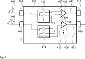
- Fig. 4 shows a block diagram of another multi-level logic analyzer 400.
- the multi-level logic analyzer 400 is based on the multi-level logic analyzer 100 and therefore also comprises signal inputs 403, 404, first switching means 413, 414, comparison units 405, 406, and the signal outputs 415, 416. The above description also applies to these elements of the multi-level logic analyzer 400.
- the first switching means 413, 414 of the multi-level logic analyzer 400 further may couple one of the signal inputs 403, 404 with a first comparator input 407, 408 of one of the comparison units 405, 406 and another one of the signal inputs 403, 404 with the second comparator input 409, 410 of the respective comparison unit 405, 406.
- This feature of the first switching means 413, 414 is shown only for the first switching means 414 but may be implemented by any other switching means.
- Fig. 5 shows a flow diagram of a method for operating a multi-level logic analyzer 100, 200, 300, 400 for analyzing multi-level digital signals 101, 102, 201, 202, 301, 302, 401, 402.
- the method comprises receiving S1 multi-level digital signals 101, 102, 201, 202, 301, 302, 401, 402, e.g. each via a signal input 103, 104, 203, 204, 303, 304, 403, 404 of the multi-level logic analyzer 100, 200, 300, 400.
- the method further comprises controllably coupling S2 at least one of the signal inputs 103, 104, 203, 204, 303, 304, 403, 404 with first comparator inputs 107, 108, 207, 208, 307, 308, 407, 408 of at least two comparison units 105, 106, 205, 206, 305, 306, 405, 406.
- the comparison units 105, 106, 205, 206, 305, 306, 405, 406 each may comprises a first comparator input 107, 108, 207, 208, 307, 308, 407, 408 and a second comparator input 109, 110, 209, 210, 309, 310, 409, 410.
- the method also comprises comparing S3 the signal received at the first comparator input 107, 108, 207, 208, 307, 308, 407, 408 of a respective comparison unit 105, 106, 205, 206, 305, 306, 405, 406 with a signal received at the second comparator input 109, 110, 209, 210, 309, 310, 409, 410 of the respective comparison unit 105, 106, 205, 206, 305, 306, 405, 406.
- the comparator output signals 111, 112, 211, 212, 311, 312, 411, 412 may e.g. be output with a plurality of signal outputs 115, 116, 215, 216, 315, 316, 415, 416.
- a single multi-level digital signal 101, 102, 201, 202, 301, 302, 401, 402 will be provided to at least two comparison units 105, 106, 205, 206, 305, 306, 405, 406 and may therefore be analyzed for multiple signal levels at the same time by the at least two comparison units 105, 106, 205, 206, 305, 306, 405, 406.
- the method may comprise coupling one of the signal inputs 103, 104, 203, 204, 303, 304, 403, 404 with a first comparator input 107, 108, 207, 208, 307, 308, 407, 408 of one of the comparison units 105, 106, 205, 206, 305, 306, 405, 406 and another one of the signal inputs 103, 104, 203, 204, 303, 304, 403, 404 with the second comparator input 109, 110, 209, 210, 309, 310, 409, 410 of the respective comparison unit 105, 106, 205, 206, 305, 306, 405, 406.
- the method may comprise controllably coupling comparison units 105, 106, 205, 206, 305, 306, 405, 406 that are coupled on their first comparison input with the same signal input 103, 104, 203, 204, 303, 304, 403, 404 on their output side with one of the signal outputs 115, 116, 215, 216, 315, 316, 415, 416.
- the output signals of the comparison units 105, 106, 205, 206, 305, 306, 405, 406 that are connected to one of the signal outputs 115, 116, 215, 216, 315, 316, 415, 416 may then be encoded into binary values or serialized.
- the method may comprise controllably coupling comparison units 105, 106, 205, 206, 305, 306, 405, 406 that are coupled on their input side with a single signal input 103, 104, 203, 204, 303, 304, 403, 404 on their output side with different signal outputs 115, 116, 215, 216, 315, 316, 415, 416.
- 401, 402 configured output voltages may be provided with a plurality of configurable threshold voltage sources 319, 320.
- one of the threshold voltage sources 319, 320 may e.g. be coupled with at least two of the comparison units 105, 106, 205, 206, 305, 306, 405, 406, especially when the respective two of the comparison units 105, 106, 205, 206, 305, 306, 405, 406 are coupled to different signal inputs 103, 104, 203, 204, 303, 304, 403, 404.
Landscapes
- Physics & Mathematics (AREA)
- General Physics & Mathematics (AREA)
- Engineering & Computer Science (AREA)
- General Engineering & Computer Science (AREA)
- Logic Circuits (AREA)
- Tests Of Electronic Circuits (AREA)
Abstract
Description
- The present invention relates to a multi-level logic analyzer for analyzing multi-level digital signals. The present invention further relates to a method for operating a multi-level logic analyzer.
- Although applicable in principal to any measurement system, the present invention and its underlying problem will be hereinafter described in combination with oscilloscopes.
- In today's modern electronic industry a variety of different measurements and tests must be performed on electronic products during development and production.
- For example oscilloscopes maybe used to record analogue voltage and/or current values. In addition, some oscilloscopes or logic analyzers allow recording logic values, where the logic state, i.e. true/false, 1/0 or on/off, is recorded. Such logic values only show the logical content of the signals but cannot represent the waveform any more.
- If a device under test uses multi-level signals, like e.g. PAM3 signals with three logic states, these signals may e.g. be recorded with an analogue input of an oscilloscope and the user may manually evaluate the different signal levels or provide the recorded signal levels from the oscilloscope e.g. to a computer to perform an automated evaluation. The oscilloscope may also provide a multi-level signal evaluation after recording the signal via an analogue input or channel.
- Against this background, the problem addressed by the present invention is providing an improved measurement of multi-level signals.
- The present invention solves this object by a multi-level logic analyzer with the features of claim 1, and by a method for operating a multi-level logic analyzer with the features of claim 10.
- Accordingly it is provided:
- A multi-level logic analyzer for analyzing multi-level digital signals, the multi-level logic analyzer comprising a plurality, i.e. two or more, of signal inputs, each signal input being configured to receive a multi-level digital signal, a plurality, i.e. two or more, of comparison units, e.g. comparators, each comparison unit comprising a first comparator input and a second comparator input and being configured to compare a signal received at the first comparator input with a signal received at the second comparator input, and first switching means configured to couple at least one of the signal inputs with the first comparator inputs of at least two of the comparison units.
- Further, it is provided:
- A method for operating a multi-level logic analyzer for analyzing multi-level digital signals, the method comprising receiving multi-level digital signals, each with a signal input, controllably coupling at least one of the signal inputs with first comparator inputs of at least two comparison units, each comparison unit comprising a first comparator input and a second comparator input, and comparing the signal received at the first comparator input of a respective comparison unit with a signal received at the second comparator input of a respective comparison unit.
- The present invention provides a multi-level logic analyzer with a plurality of signal inputs. Plurality in this context may refer to any number larger than one. Further, the multi-level logic analyzer provides a plurality of comparison units that compare two signals at their inputs.
- In addition, first switching means may couple the single signal inputs each with at least two of the comparison units.
- This arrangement of the multi-level logic analyzer allows analyzing multi-level signals without the need to use e.g. an analogue channel of an oscilloscope. The number of analogue channels on an oscilloscope is usually limited, e.g. to four. With the present invention these analogue channels may be reserved for analogue measurements and the multi-level signals may be measured via the multi-level logic analyzer that may e.g. be integrated into an oscilloscope or the like.
- The first switching means may e.g. couple a single signal input to as many comparison units as the signal has logic levels or signal levels. If for example a signal is a PAM3 signal with three logic levels, the respective signal input may be coupled to two of the comparison units. Only two of the comparison units are needed, since one of the signal levels is the zero level.
- The two comparison units may then e.g. have different switching levels that represent the logic levels of the input signal. If the logic level of the input signal is the first or lowest logic level, none of the comparison units will output a signal or they will output a zero or low signal. If the logic level of the input signal is the second level, only the first of the comparison units will output a positive signal. If the logic level of the input signal is the third level, both of the comparison units will output a positive signal.
- The output of the comparison units may then further be processed to evaluate the number of positive outputs and determine the signal level of the multi-level signal.
- The comparison units may e.g. be comparators or subtractors and the first comparator inputs may be the positive inputs of the comparators or subtractors, and the second comparator inputs may be the negative inputs of the comparators or subtractors. This will lead to an inverse output. The signal inputs may also be switched. This will provide a normal or noninverted output.
- Further embodiments of the present invention are subject of the further subclaims and of the following description, referring to the drawings.
- In a possible embodiment, the multi-level logic analyzer may comprise a plurality, i.e. two or more, of signal outputs, each signal output being configured to output an output signal.
- The signal outputs may provide the output signals to following signal processing units. In addition, the signal outputs may perform any kind of signal conditioning. The signal outputs may output any kind of signal, like e.g. an analogue or a digital serial or parallel signal.
- In a possible embodiment, the multi-level logic analyzer may comprise second switching means configured to controllably couple comparison units that are coupled on their first comparison input with the same signal input on their output side with one of the signal outputs.
- If different comparison units are coupled to a single signal input, they may each serve to analyze a different level of the multi-level logic signal that is provided as input signal to the respective signal input. Coupling all of these comparison units to a single output allows providing a following signal processing unit with a single signal that represents the different signal levels of the multi-level input signal.
- In a possible embodiment, the signal outputs may comprise an encoder that is configured to encode output signals of the comparison units that are connected to the respective signal output into binary values or serialize the output signals of the respective comparison units.
- As already described above, in an exemplary embodiment the number of comparison units that show a positive or high value represents the momentary level present at the multi-level input signal. Therefore, encoding this number into a binary value or a serial digital signal allows providing the following signal processing unit with an indication of the momentary level of the multi-level input signal that is easily usable in digital systems.
- In a possible embodiment, the second switching means may further be configured to controllably couple comparison units that are coupled on their input side with a single signal input on their output side with different signal outputs.
- This allows providing the results of the single comparison units as a raw signal to a following signal processing unit and performing any type of analysis on these raw signals in the following signal processing unit.
- In a possible embodiment, the multi-level logic analyzer may comprise a plurality, i.e. two or more, of configurable threshold voltage sources, each threshold voltage source being configured to provide a configured output voltage.
- The configurable threshold voltage sources may serve in the multi-level logic analyzer to provide the comparison units with respective threshold voltages as a basis for performing the comparison of the multi-level input signal to determine the momentary level of the multi-level input signal. This means that the comparison units will compare the respective threshold voltage with the input signal provided to the respective comparison unit.
- In a possible embodiment, the multi-level logic analyzer may comprise a plurality, i.e. two or more, of third switching means being configured to couple one of the threshold voltage sources with at least two of the comparison units, especially when the respective two of the comparison units are coupled to different signal inputs.
- If two of the comparison units are provided with the same threshold voltage, their output will be triggered by the same signal levels on the input sides. Therefore, two different input signals at two different signal inputs may be compared with the same threshold voltage.
- In a possible embodiment, the threshold voltage sources may be configured to each output a different threshold voltage.
- Since the threshold voltage sources are configurable, it is possible to configure each one of the threshold voltage sources according to a predetermined signal level of the received multi-level signal.
- For example, for a three level multi-level signal two of the threshold voltage sources may be configured to provide threshold voltages, which are in the middle of the voltage range between the respective voltage levels of the multi-level signal.
- If for example a first level of the of the multi-level signal is 0 V, a second level of the multi-level signal is 2,5 V and a third level of the multi-level signal is 5 V, a first threshold voltage source could be configured to provide 1,25 V, and a second threshold voltage source could be configured to provide 3,75 V.
- In a possible embodiment, the first switching means may further be configured to couple one of the signal inputs with a first comparator input of one of the comparison units and one of the signal inputs with the second comparator input of the respective comparison unit.
- If two signal inputs are connected to the same comparison unit, e.g. a subtractor like a differential amplifier or the like, but each to a different comparator input of the comparison unit, it is possible to measure differential signals. It is understood, that the signal inputs may be coupled to various different comparison units at the same time and that differential multi-level signals may be processed with the present invention.
- For a more complete understanding of the present invention and advantages thereof, reference is now made to the following description taken in conjunction with the accompanying drawings. The invention is explained in more detail below using exemplary embodiments which are specified in the schematic figures of the drawings, in which:
- Fig. 1
- shows a block diagram of an embodiment of a multi-level logic analyzer according to the present invention;
- Fig. 2
- shows a block diagram of another embodiment of a multi-level logic analyzer according to the present invention;
- Fig. 3
- shows a block diagram of another embodiment of a multi-level logic analyzer according to the present invention;
- Fig. 4
- shows a block diagram of another embodiment of a multi-level logic analyzer according to the present invention; and
- Fig. 5
- shows a flow diagram of a method for operating a multi-level logic analyzer according to the present invention.
- The appended drawings are intended to provide further understanding of the embodiments of the invention. They illustrate embodiments and, in conjunction with the description, help to explain principles and concepts of the invention. Other embodiments and many of the advantages mentioned become apparent in view of the drawings. The elements in the drawings are not necessarily shown to scale.
- In the drawings, like, functionally equivalent and identically operating elements, features and components are provided with like reference signs in each case, unless stated otherwise.
-
Fig. 1 shows a block diagram of amulti-level logic analyzer 100 for analyzing multi-leveldigital signals digital signals Fig. 1 just exemplarily comprise three voltage levels. It is however understood that the present invention may be applied to multi-level digital signals with any number of signal levels. - The
multi-level logic analyzer 100 comprises a plurality of signal inputs, wherein only twosignal inputs - The
multi-level logic analyzer 100 further comprises for every one of thesignal inputs 103, 104 a first switching means 113, 114. As with thesignal inputs multi-level logic analyzer 100 comprises a plurality ofcomparison units comparison units respective signal outputs comparator outputs - The first switching means 113, 114 each receive one of the multi-level
digital signals digital signals comparison units digital signals digital signals many comparison units digital signals - For example the first switching means 113 may forward the multi-level
digital signal 101 to the two shown first switching means 113, 114. The first switching means 114 may forward the multi-leveldigital signal 102 to two further not shown comparison units. This allows themulti-level logic analyzer 100 to process multiple multi-leveldigital signals - The
comparison units digital signal 101 via afirst comparator input digital signal 101 may be provided on thesecond comparator inputs comparison units first comparator input second comparator input digital signal 101, and the comparison voltage of the first switching means 114 may e.g. be between the second and the third signal level of the multi-leveldigital signal 101. - This means that both
comparison units digital signal 101 has the first signal level. Thecomparison unit 105 will provide a positive output, when the multi-leveldigital signal 101 has the second signal level, and bothcomparison units digital signal 101 has the third signal level. - The above may be applied to any number of multi-level
digital signals - It is therefore not necessary to use e.g. an analogue channel of an oscilloscope to perform multi-level measurements.
- It is understood, that the first switching means 113, 114 may e.g. be combined into a switching matrix that may comprise any number of switches, like e.g. digitally controllable switches. It is further understood, that the
multi-level logic analyzer 100 may comprise any further elements, like e.g. filters, amplifier, and attenuators that are necessary to receive or output the multi-leveldigital signals multi-level logic analyzer 100 may comprise a control unit that configures the first switching means 113, 114 and any other configurable element of themulti-level logic analyzer 100 e.g. based on test parameters or a user input. -
Fig. 2 shows a block diagram of anothermulti-level logic analyzer 200. Themulti-level logic analyzer 200 is based on themulti-level logic analyzer 100 and therefore also comprisessignal inputs comparison units multi-level logic analyzer 200. - In addition, the
multi-level logic analyzer 200 comprises second switching means 217 that are coupled between thecomparison units digital signals - The second switching means 217 may controllably couple the
comparison units same signal input - This means that the comparator output signals 211, 212 of
multiple comparison units single signal output digital signal Fig. 1 , the first switching means 213 provides the multi-leveldigital signal 201 to the twocomparison units same signal output 215. Thesignal output 215 comprises anencoder 218. Even if it is not expressly shown, it is clear that all other signal outputs may also comprise an encoder. - The
encoder 218 may encode the parallel comparator output signals 211, 212 of therespective comparison units encoder 218 may also serialize the output signals of therespective comparison units encoder 218 therefore provides the signal level in a binary format that may easily be processed by any following signal processing unit. - The second switching means 217 may as an alternative couple the
comparison units different signal outputs -
Fig. 3 shows a block diagram of another embodiment of amulti-level logic analyzer 300. Themulti-level logic analyzer 300 is based on themulti-level logic analyzer 200 and therefore also comprisessignal inputs comparison units encoder 318. - The above description therefore also applies to these elements of the
multi-level logic analyzer 300. - In addition, the
multi-level logic analyzer 300 comprises a plurality of configurablethreshold voltage sources threshold voltage sources comparison units digital signals threshold voltage sources - The
multi-level logic analyzer 300 further comprises a plurality of third switching means 321, 322, of which only two are shown for sake of clarity. The third switching means 321, 322 may couple one of thethreshold voltage sources comparison units comparison units different signal inputs digital signals threshold voltage source multiple comparison units -
Fig. 4 shows a block diagram of anothermulti-level logic analyzer 400. Themulti-level logic analyzer 400 is based on themulti-level logic analyzer 100 and therefore also comprisessignal inputs comparison units multi-level logic analyzer 400. - In addition to the
multi-level logic analyzer 100, the first switching means 413, 414 of themulti-level logic analyzer 400 further may couple one of thesignal inputs first comparator input comparison units signal inputs second comparator input respective comparison unit - With such first switching means 413, 414 it is possible to analyze differential multi-level
digital signals - For sake of clarity in the following description of the method based
Fig. 5 the reference signs used above in the description of apparatus basedFigs. 1 - 4 will be maintained. -
Fig. 5 shows a flow diagram of a method for operating amulti-level logic analyzer digital signals - The method comprises receiving S1 multi-level
digital signals signal input multi-level logic analyzer signal inputs first comparator inputs comparison units comparison units first comparator input second comparator input first comparator input respective comparison unit second comparator input respective comparison unit signal outputs - With the present method, a single multi-level
digital signal comparison units comparison units - For the processing of differential multi-level
digital signals signal inputs first comparator input comparison units signal inputs second comparator input respective comparison unit - The method may comprise controllably coupling
comparison units same signal input comparison units - In addition, the method may comprise controllably coupling
comparison units single signal input different signal outputs - In order to perform a comparison of the multi-level
digital signals threshold voltage sources threshold voltage sources comparison units comparison units different signal inputs - Although specific embodiments have been illustrated and described herein, it will be appreciated by those of ordinary skill in the art that a variety of alternate and/or equivalent implementations exist. It should be appreciated that the exemplary embodiment or exemplary embodiments are only examples, and are not intended to limit the scope, applicability, or configuration in any way. Rather, the foregoing summary and detailed description will provide those skilled in the art with a convenient road map for implementing at least one exemplary embodiment, it being understood that various changes may be made in the function and arrangement of elements described in an exemplary embodiment without departing from the scope as set forth in the appended claims and their legal equivalents. Generally, this application is intended to cover any adaptations or variations of the specific embodiments discussed herein.
- In the foregoing detailed description, various features are grouped together in one or more examples or examples for the purpose of streamlining the disclosure. It is understood that the above description is intended to be illustrative, and not restrictive. It is intended to cover all alternatives, modifications and equivalents as may be included within the scope of the invention. Many other examples will be apparent to one skilled in the art upon reviewing the above specification.
- Specific nomenclature used in the foregoing specification is used to provide a thorough understanding of the invention. However, it will be apparent to one skilled in the art in light of the specification provided herein that the specific details are not required in order to practice the invention. Thus, the foregoing descriptions of specific embodiments of the present invention are presented for purposes of illustration and description. They are not intended to be exhaustive or to limit the invention to the precise forms disclosed; obviously many modifications and variations are possible in view of the above teachings. The embodiments were chosen and described in order to best explain the principles of the invention and its practical applications, to thereby enable others skilled in the art to best utilize the invention and various embodiments with various modifications as are suited to the particular use contemplated. Throughout the specification, the terms "including" and "in which" are used as the plain-English equivalents of the respective terms "comprising" and "wherein," respectively. Moreover, the terms "first," "second," and "third," etc., are used merely as labels, and are not intended to impose numerical requirements on or to establish a certain ranking of importance of their objects.
-
- 100, 200, 300, 400
- multi-level logic analyzer
- 101, 102, 201, 202, 301, 302
- multi-level digital signal
- 401, 402
- multi-level digital signal
- 103, 104, 203, 204, 303, 304
- signal input
- 403, 404
- signal input
- 105, 106, 205, 206, 305, 306
- comparison unit
- 405, 406
- comparison unit
- 107, 108, 207, 208, 307, 308
- first comparator input
- 407, 408
- first comparator input
- 109, 110, 209, 210, 309, 310
- second comparator input
- 409, 410
- second comparator input
- 111, 112, 211, 212, 311, 312
- comparator output
- 411, 412
- comparator output
- 113, 114, 213, 214, 313, 314
- first switching means
- 413, 414
- first switching means
- 115, 116, 215, 216, 315, 316
- signal output
- 415, 416
- signal output
- 217, 317
- second switching means
- 218, 318
- encoder
- 319, 320
- threshold voltage source
- 321, 322
- third switching means
- S1 - S3
- method steps
Claims (15)
- Multi-level logic analyzer (100, 200, 300, 400) for analyzing multi-level digital signals (101, 102, 201, 202, 301, 302, 401, 402), the multi-level logic analyzer (100, 200, 300, 400) comprising:a plurality of signal inputs (103, 104, 203, 204, 303, 304, 403, 404), each signal input (103, 104, 203, 204, 303, 304, 403, 404) being configured to receive a multi-level digital signal (101, 102, 201, 202, 301, 302, 401, 402),a plurality of comparison units (105, 106, 205, 206, 305, 306, 405, 406), each comparison unit (105, 106, 205, 206, 305, 306, 405, 406) comprising a first comparator input (107, 108, 207, 208, 307, 308, 407, 408) and a second comparator input (109, 110, 209, 210, 309, 310, 409, 410) and being configured to compare a signal received at the first comparator input (107, 108, 207, 208, 307, 308, 407, 408) with a signal received at the second comparator input (109, 110, 209, 210, 309, 310, 409, 410), andfirst switching means (113, 114, 213, 214, 313, 314, 413, 414) configured to couple at least one of the signal inputs (103, 104, 203, 204, 303, 304, 403, 404) with the first comparator inputs (107, 108, 207, 208, 307, 308, 407, 408) of at least two of the comparison units (105, 106, 205, 206, 305, 306, 405, 406).
- Multi-level logic analyzer (100, 200, 300, 400) according to claim 1, comprising a plurality of signal outputs (115, 116, 215, 216, 315, 316, 415, 416), each signal output (115, 116, 215, 216, 315, 316, 415, 416) being configured to output an output signal.
- Multi-level logic analyzer (100, 200, 300, 400) according to claim 2, comprising second switching means (217, 317) configured to controllably couple comparison units (105, 106, 205, 206, 305, 306, 405, 406) that are coupled on their first comparison input with the same signal input (103, 104, 203, 204, 303, 304, 403, 404) on their output side with one of the signal outputs (115, 116, 215, 216, 315, 316, 415, 416).
- Multi-level logic analyzer (100, 200, 300, 400) according to claim 3, wherein the signal outputs (115, 116, 215, 216, 315, 316, 415, 416) comprise an encoder (218, 318) that encodes output signals of the comparison units (105, 106, 205, 206, 305, 306, 405, 406) that are connected to the respective signal output (115, 116, 215, 216, 315, 316, 415, 416) into binary values or serializes the output signals of the respective comparison units (105, 106, 205, 206, 305, 306, 405, 406).
- Multi-level logic analyzer (100, 200, 300, 400) according to claim 3, wherein the second switching means (217, 317) are further configured to controllably couple comparison units (105, 106, 205, 206, 305, 306, 405, 406) that are coupled on their input side with a single signal input (103, 104, 203, 204, 303, 304, 403, 404) on their output side with different signal outputs (115, 116, 215, 216, 315, 316, 415, 416).
- Multi-level logic analyzer (100, 200, 300, 400) according to any one of the preceding claims, comprising a plurality of configurable threshold voltage sources (319, 320), each threshold voltage source (319, 320) being configured to provide a configured output voltage.
- Multi-level logic analyzer (100, 200, 300, 400) according to claim 6, comprising a plurality of third switching means (321, 322) being configured to couple one of the threshold voltage sources (319, 320) with at least two of the comparison units (105, 106, 205, 206, 305, 306, 405, 406), especially when the respective two of the comparison units (105, 106, 205, 206, 305, 306, 405, 406) are coupled to different signal inputs (103, 104, 203, 204, 303, 304, 403, 404).
- Multi-level logic analyzer (100, 200, 300, 400) according to claim 6, wherein the threshold voltage sources (319, 320) are configured to each output a different threshold voltage.
- Multi-level logic analyzer (100, 200, 300, 400) according to any one of the preceding claims, wherein the first switching means (113, 114, 213, 214, 313, 314, 413, 414) are further configured to couple one of the signal inputs (103, 104, 203, 204, 303, 304, 403, 404) with a first comparator input (107, 108, 207, 208, 307, 308, 407, 408) of one of the comparison units (105, 106, 205, 206, 305, 306, 405, 406) and another one of the signal inputs (103, 104, 203, 204, 303, 304, 403, 404) with the second comparator input (109, 110, 209, 210, 309, 310, 409, 410) of the respective comparison unit (105, 106, 205, 206, 305, 306, 405, 406).
- Method for operating a multi-level logic analyzer (100, 200, 300, 400) for analyzing multi-level digital signals (101, 102, 201, 202, 301, 302, 401, 402), the method comprising:receiving (S1) multi-level digital signals (101, 102, 201, 202, 301, 302, 401, 402), each with a signal input (103, 104, 203, 204, 303, 304, 403, 404),controllably coupling (S2) at least one of the signal inputs (103, 104, 203, 204, 303, 304, 403, 404) with first comparator inputs (107, 108, 207, 208, 307, 308, 407, 408) of at least two comparison units (105, 106, 205, 206, 305, 306, 405, 406), each comparison unit (105, 106, 205, 206, 305, 306, 405, 406) comprising a first comparator input (107, 108, 207, 208, 307, 308, 407, 408) and a second comparator input (109, 110, 209, 210, 309, 310, 409, 410), andcomparing (S3) the signal received at the first comparator input (107, 108, 207, 208, 307, 308, 407, 408) of a respective comparison unit (105, 106, 205, 206, 305, 306, 405, 406) with a signal received at the second comparator input (109, 110, 209, 210, 309, 310, 409, 410) of a respective comparison unit (105, 106, 205, 206, 305, 306, 405, 406).
- Method according to claim 10, comprising outputting an output signal with a plurality of signal outputs (115, 116, 215, 216, 315, 316, 415, 416).
- Method according to claim 11, comprising controllably coupling comparison units (105, 106, 205, 206, 305, 306, 405, 406) that are coupled on their first comparison input with the same signal input (103, 104, 203, 204, 303, 304, 403, 404) on their output side with one of the signal outputs (115, 116, 215, 216, 315, 316, 415, 416), and especially comprising encoding the output signals of the comparison units (105, 106, 205, 206, 305, 306, 405, 406) that are connected to one of the signal outputs (115, 116, 215, 216, 315, 316, 415, 416) into binary values or serializing the output signals of the respective comparison units (105, 106, 205, 206, 305, 306, 405, 406), especially in the respective signal outputs (115, 116, 215, 216, 315, 316, 415, 416), and/or comprising controllably coupling comparison units (105, 106, 205, 206, 305, 306, 405, 406) that are coupled on their input side with a single signal input (103, 104, 203, 204, 303, 304, 403, 404) on their output side with different signal outputs (115, 116, 215, 216, 315, 316, 415, 416).
- Method according to any one of the preceding claims 10 - 12, comprising providing configured output voltages with a plurality of configurable threshold voltage sources (319, 320).
- Method according to claim 13, comprising coupling one of the threshold voltage sources (319, 320) with at least two of the comparison units (105, 106, 205, 206, 305, 306, 405, 406), especially when the respective two of the comparison units (105, 106, 205, 206, 305, 306, 405, 406) are coupled to different signal inputs (103, 104, 203, 204, 303, 304, 403, 404); and/or
wherein the threshold voltage sources (319, 320) each output a different threshold voltage. - Method according to any one of the preceding claims 10 - 14, comprising coupling one of the signal inputs (103, 104, 203, 204, 303, 304, 403, 404) with a first comparator input (107, 108, 207, 208, 307, 308, 407, 408) of one of the comparison units (105, 106, 205, 206, 305, 306, 405, 406) and another one of the signal inputs (103, 104, 203, 204, 303, 304, 403, 404) with the second comparator input (109, 110, 209, 210, 309, 310, 409, 410) of the respective comparison unit (105, 106, 205, 206, 305, 306, 405, 406).
Priority Applications (3)
| Application Number | Priority Date | Filing Date | Title |
|---|---|---|---|
| EP17162481.0A EP3379274B1 (en) | 2017-03-23 | 2017-03-23 | Multi-level logic analyzer for analyzing multi-level digital signals and method for operating a multi-level logic analyzer for analyzing multi-level digital signals |
| US15/823,841 US10809282B2 (en) | 2017-03-23 | 2017-11-28 | Multi-level logic analyzer for analyzing multi-level digital signals and method for operating a multi-level logic analyzer for analyzing multi-level digital signals |
| CN201810022543.1A CN108627719B (en) | 2017-03-23 | 2018-01-10 | Multilevel logic analyzer for analyzing multilevel digital signals and method of operating the same |
Applications Claiming Priority (1)
| Application Number | Priority Date | Filing Date | Title |
|---|---|---|---|
| EP17162481.0A EP3379274B1 (en) | 2017-03-23 | 2017-03-23 | Multi-level logic analyzer for analyzing multi-level digital signals and method for operating a multi-level logic analyzer for analyzing multi-level digital signals |
Publications (2)
| Publication Number | Publication Date |
|---|---|
| EP3379274A1 true EP3379274A1 (en) | 2018-09-26 |
| EP3379274B1 EP3379274B1 (en) | 2021-04-28 |
Family
ID=58410170
Family Applications (1)
| Application Number | Title | Priority Date | Filing Date |
|---|---|---|---|
| EP17162481.0A Active EP3379274B1 (en) | 2017-03-23 | 2017-03-23 | Multi-level logic analyzer for analyzing multi-level digital signals and method for operating a multi-level logic analyzer for analyzing multi-level digital signals |
Country Status (3)
| Country | Link |
|---|---|
| US (1) | US10809282B2 (en) |
| EP (1) | EP3379274B1 (en) |
| CN (1) | CN108627719B (en) |
Citations (5)
| Publication number | Priority date | Publication date | Assignee | Title |
|---|---|---|---|---|
| DE3120622A1 (en) * | 1981-05-23 | 1982-12-16 | Rohde & Schwarz GmbH & Co KG, 8000 München | Logic analyser |
| US5177483A (en) * | 1988-06-17 | 1993-01-05 | U.S. Philips Corporation | Multilevel configurable logic analyzer |
| JPH05249190A (en) * | 1992-03-06 | 1993-09-28 | Sharp Corp | LSI tester |
| JPH102937A (en) * | 1996-06-13 | 1998-01-06 | Yokogawa Electric Corp | IC test equipment |
| US20040008052A1 (en) * | 2002-07-11 | 2004-01-15 | Hideaki Sakaguchi | Semiconductor testing apparatus and semiconductor testing method |
Family Cites Families (6)
| Publication number | Priority date | Publication date | Assignee | Title |
|---|---|---|---|---|
| CA2442922A1 (en) | 2001-04-04 | 2002-10-17 | Quellan, Inc. | Method and system for decoding multilevel signals |
| CN100407578C (en) * | 2002-11-22 | 2008-07-30 | 模拟器件公司 | level converting digital switch |
| KR101872310B1 (en) * | 2011-12-19 | 2018-07-02 | 에스케이하이닉스 주식회사 | Rail-to-Rail Comparator and Pulse Amplitude Modulation Receiver and Communication System Using the Same |
| CN102545665B (en) * | 2012-02-09 | 2013-12-25 | 天津大学 | Three-level PWM (Pulse-Width Modulation) rectifier direct power control method |
| JP5549692B2 (en) * | 2012-02-10 | 2014-07-16 | 株式会社デンソー | Logic signal isolation transmission circuit |
| US9035815B1 (en) * | 2014-03-04 | 2015-05-19 | Xilinx, Inc. | High-speed and high-resolution signal analysis system |
-
2017
- 2017-03-23 EP EP17162481.0A patent/EP3379274B1/en active Active
- 2017-11-28 US US15/823,841 patent/US10809282B2/en active Active
-
2018
- 2018-01-10 CN CN201810022543.1A patent/CN108627719B/en active Active
Patent Citations (5)
| Publication number | Priority date | Publication date | Assignee | Title |
|---|---|---|---|---|
| DE3120622A1 (en) * | 1981-05-23 | 1982-12-16 | Rohde & Schwarz GmbH & Co KG, 8000 München | Logic analyser |
| US5177483A (en) * | 1988-06-17 | 1993-01-05 | U.S. Philips Corporation | Multilevel configurable logic analyzer |
| JPH05249190A (en) * | 1992-03-06 | 1993-09-28 | Sharp Corp | LSI tester |
| JPH102937A (en) * | 1996-06-13 | 1998-01-06 | Yokogawa Electric Corp | IC test equipment |
| US20040008052A1 (en) * | 2002-07-11 | 2004-01-15 | Hideaki Sakaguchi | Semiconductor testing apparatus and semiconductor testing method |
Also Published As
| Publication number | Publication date |
|---|---|
| US10809282B2 (en) | 2020-10-20 |
| US20180275170A1 (en) | 2018-09-27 |
| EP3379274B1 (en) | 2021-04-28 |
| CN108627719A (en) | 2018-10-09 |
| CN108627719B (en) | 2022-08-12 |
Similar Documents
| Publication | Publication Date | Title |
|---|---|---|
| US12140631B2 (en) | Measurement system for identifying aggressor signals | |
| US10852323B2 (en) | Measurement apparatus and method for analyzing a waveform of a signal | |
| JP4152323B2 (en) | Test equipment for LSI to be measured | |
| EP3705896B1 (en) | Test method and test system | |
| US6901339B2 (en) | Eye diagram analyzer correctly samples low dv/dt voltages | |
| CN114859210A (en) | CMOS chip open-short circuit test system and test method | |
| US10809282B2 (en) | Multi-level logic analyzer for analyzing multi-level digital signals and method for operating a multi-level logic analyzer for analyzing multi-level digital signals | |
| US4862069A (en) | Method of in-circuit testing | |
| US20040148549A1 (en) | Method for using an alternate performance test to reduce test time and improve manufacturing yield | |
| US20170108533A1 (en) | Test systems and methods of testing devices | |
| Razzaque Mughal et al. | Group acceptance sampling plan for re-submitted lots under generalized Pareto distribution | |
| CN112596967A (en) | Method, device and system for testing board card signal time sequence and server system | |
| US10416203B2 (en) | Test and measurement system, differential logic probe, single ended logic probe and method for operating a test and measurement system | |
| US7243033B2 (en) | Inspection apparatus | |
| US20240353449A1 (en) | Interleaved digital trigger correction | |
| US20100313091A1 (en) | Apparatus and method for testing semiconductor integrated circuit | |
| DE102008052335A1 (en) | Multipath power meter with amplifier | |
| JP4973690B2 (en) | Inspection device | |
| RU2777299C1 (en) | Method for continuous monitoring of the receiving path of the ship's hydroacoustic complex | |
| US20260002965A1 (en) | Autoset feature as part of bus configuration to automatically detect and set serial bus parameters | |
| US10965343B1 (en) | Signal analyzer and method for analyzing signals | |
| Beniugă et al. | Virtual instrumentation system for remote reading of digital and analogical equipment display | |
| JP2026008996A (en) | Test and measurement device and automatic setting method | |
| Lai et al. | Design, Implementation, and Verification of a Data Acquisition System for the Prototypes of the Front-End Electronics of the PANDA Micro Vertex Detector | |
| RU2084908C1 (en) | Device which measures nominal characteristics of electric circuits |
Legal Events
| Date | Code | Title | Description |
|---|---|---|---|
| PUAI | Public reference made under article 153(3) epc to a published international application that has entered the european phase |
Free format text: ORIGINAL CODE: 0009012 |
|
| STAA | Information on the status of an ep patent application or granted ep patent |
Free format text: STATUS: THE APPLICATION HAS BEEN PUBLISHED |
|
| AK | Designated contracting states |
Kind code of ref document: A1 Designated state(s): AL AT BE BG CH CY CZ DE DK EE ES FI FR GB GR HR HU IE IS IT LI LT LU LV MC MK MT NL NO PL PT RO RS SE SI SK SM TR |
|
| AX | Request for extension of the european patent |
Extension state: BA ME |
|
| STAA | Information on the status of an ep patent application or granted ep patent |
Free format text: STATUS: REQUEST FOR EXAMINATION WAS MADE |
|
| 17P | Request for examination filed |
Effective date: 20190214 |
|
| RBV | Designated contracting states (corrected) |
Designated state(s): AL AT BE BG CH CY CZ DE DK EE ES FI FR GB GR HR HU IE IS IT LI LT LU LV MC MK MT NL NO PL PT RO RS SE SI SK SM TR |
|
| GRAP | Despatch of communication of intention to grant a patent |
Free format text: ORIGINAL CODE: EPIDOSNIGR1 |
|
| STAA | Information on the status of an ep patent application or granted ep patent |
Free format text: STATUS: GRANT OF PATENT IS INTENDED |
|
| INTG | Intention to grant announced |
Effective date: 20201104 |
|
| GRAS | Grant fee paid |
Free format text: ORIGINAL CODE: EPIDOSNIGR3 |
|
| RBV | Designated contracting states (corrected) |
Designated state(s): AL AT BE BG CY CZ DE DK EE ES FI FR GB GR HR HU IS IT LT LU LV MC MK MT NL NO PL PT RO RS SE SI SK SM TR |
|
| GRAA | (expected) grant |
Free format text: ORIGINAL CODE: 0009210 |
|
| STAA | Information on the status of an ep patent application or granted ep patent |
Free format text: STATUS: THE PATENT HAS BEEN GRANTED |
|
| AK | Designated contracting states |
Kind code of ref document: B1 Designated state(s): AL AT BE BG CY CZ DE DK EE ES FI FR GB GR HR HU IS IT LT LU LV MC MK MT NL NO PL PT RO RS SE SI SK SM TR |
|
| REG | Reference to a national code |
Ref country code: GB Ref legal event code: FG4D |
|
| REG | Reference to a national code |
Ref country code: AT Ref legal event code: REF Ref document number: 1387665 Country of ref document: AT Kind code of ref document: T Effective date: 20210515 |
|
| REG | Reference to a national code |
Ref country code: DE Ref legal event code: R096 Ref document number: 602017037436 Country of ref document: DE |
|
| REG | Reference to a national code |
Ref country code: LT Ref legal event code: MG9D |
|
| REG | Reference to a national code |
Ref country code: AT Ref legal event code: MK05 Ref document number: 1387665 Country of ref document: AT Kind code of ref document: T Effective date: 20210428 |
|
| PG25 | Lapsed in a contracting state [announced via postgrant information from national office to epo] |
Ref country code: NL Free format text: LAPSE BECAUSE OF FAILURE TO SUBMIT A TRANSLATION OF THE DESCRIPTION OR TO PAY THE FEE WITHIN THE PRESCRIBED TIME-LIMIT Effective date: 20210428 Ref country code: HR Free format text: LAPSE BECAUSE OF FAILURE TO SUBMIT A TRANSLATION OF THE DESCRIPTION OR TO PAY THE FEE WITHIN THE PRESCRIBED TIME-LIMIT Effective date: 20210428 Ref country code: AT Free format text: LAPSE BECAUSE OF FAILURE TO SUBMIT A TRANSLATION OF THE DESCRIPTION OR TO PAY THE FEE WITHIN THE PRESCRIBED TIME-LIMIT Effective date: 20210428 Ref country code: BG Free format text: LAPSE BECAUSE OF FAILURE TO SUBMIT A TRANSLATION OF THE DESCRIPTION OR TO PAY THE FEE WITHIN THE PRESCRIBED TIME-LIMIT Effective date: 20210728 Ref country code: FI Free format text: LAPSE BECAUSE OF FAILURE TO SUBMIT A TRANSLATION OF THE DESCRIPTION OR TO PAY THE FEE WITHIN THE PRESCRIBED TIME-LIMIT Effective date: 20210428 Ref country code: LT Free format text: LAPSE BECAUSE OF FAILURE TO SUBMIT A TRANSLATION OF THE DESCRIPTION OR TO PAY THE FEE WITHIN THE PRESCRIBED TIME-LIMIT Effective date: 20210428 |
|
| PG25 | Lapsed in a contracting state [announced via postgrant information from national office to epo] |
Ref country code: LV Free format text: LAPSE BECAUSE OF FAILURE TO SUBMIT A TRANSLATION OF THE DESCRIPTION OR TO PAY THE FEE WITHIN THE PRESCRIBED TIME-LIMIT Effective date: 20210428 Ref country code: IS Free format text: LAPSE BECAUSE OF FAILURE TO SUBMIT A TRANSLATION OF THE DESCRIPTION OR TO PAY THE FEE WITHIN THE PRESCRIBED TIME-LIMIT Effective date: 20210828 Ref country code: GR Free format text: LAPSE BECAUSE OF FAILURE TO SUBMIT A TRANSLATION OF THE DESCRIPTION OR TO PAY THE FEE WITHIN THE PRESCRIBED TIME-LIMIT Effective date: 20210729 Ref country code: NO Free format text: LAPSE BECAUSE OF FAILURE TO SUBMIT A TRANSLATION OF THE DESCRIPTION OR TO PAY THE FEE WITHIN THE PRESCRIBED TIME-LIMIT Effective date: 20210728 Ref country code: PL Free format text: LAPSE BECAUSE OF FAILURE TO SUBMIT A TRANSLATION OF THE DESCRIPTION OR TO PAY THE FEE WITHIN THE PRESCRIBED TIME-LIMIT Effective date: 20210428 Ref country code: PT Free format text: LAPSE BECAUSE OF FAILURE TO SUBMIT A TRANSLATION OF THE DESCRIPTION OR TO PAY THE FEE WITHIN THE PRESCRIBED TIME-LIMIT Effective date: 20210830 Ref country code: SE Free format text: LAPSE BECAUSE OF FAILURE TO SUBMIT A TRANSLATION OF THE DESCRIPTION OR TO PAY THE FEE WITHIN THE PRESCRIBED TIME-LIMIT Effective date: 20210428 Ref country code: RS Free format text: LAPSE BECAUSE OF FAILURE TO SUBMIT A TRANSLATION OF THE DESCRIPTION OR TO PAY THE FEE WITHIN THE PRESCRIBED TIME-LIMIT Effective date: 20210428 |
|
| REG | Reference to a national code |
Ref country code: NL Ref legal event code: MP Effective date: 20210428 |
|
| PG25 | Lapsed in a contracting state [announced via postgrant information from national office to epo] |
Ref country code: SM Free format text: LAPSE BECAUSE OF FAILURE TO SUBMIT A TRANSLATION OF THE DESCRIPTION OR TO PAY THE FEE WITHIN THE PRESCRIBED TIME-LIMIT Effective date: 20210428 Ref country code: SK Free format text: LAPSE BECAUSE OF FAILURE TO SUBMIT A TRANSLATION OF THE DESCRIPTION OR TO PAY THE FEE WITHIN THE PRESCRIBED TIME-LIMIT Effective date: 20210428 Ref country code: CZ Free format text: LAPSE BECAUSE OF FAILURE TO SUBMIT A TRANSLATION OF THE DESCRIPTION OR TO PAY THE FEE WITHIN THE PRESCRIBED TIME-LIMIT Effective date: 20210428 Ref country code: EE Free format text: LAPSE BECAUSE OF FAILURE TO SUBMIT A TRANSLATION OF THE DESCRIPTION OR TO PAY THE FEE WITHIN THE PRESCRIBED TIME-LIMIT Effective date: 20210428 Ref country code: DK Free format text: LAPSE BECAUSE OF FAILURE TO SUBMIT A TRANSLATION OF THE DESCRIPTION OR TO PAY THE FEE WITHIN THE PRESCRIBED TIME-LIMIT Effective date: 20210428 Ref country code: RO Free format text: LAPSE BECAUSE OF FAILURE TO SUBMIT A TRANSLATION OF THE DESCRIPTION OR TO PAY THE FEE WITHIN THE PRESCRIBED TIME-LIMIT Effective date: 20210428 Ref country code: ES Free format text: LAPSE BECAUSE OF FAILURE TO SUBMIT A TRANSLATION OF THE DESCRIPTION OR TO PAY THE FEE WITHIN THE PRESCRIBED TIME-LIMIT Effective date: 20210428 |
|
| REG | Reference to a national code |
Ref country code: DE Ref legal event code: R097 Ref document number: 602017037436 Country of ref document: DE |
|
| PLBE | No opposition filed within time limit |
Free format text: ORIGINAL CODE: 0009261 |
|
| STAA | Information on the status of an ep patent application or granted ep patent |
Free format text: STATUS: NO OPPOSITION FILED WITHIN TIME LIMIT |
|
| 26N | No opposition filed |
Effective date: 20220131 |
|
| PG25 | Lapsed in a contracting state [announced via postgrant information from national office to epo] |
Ref country code: IS Free format text: LAPSE BECAUSE OF FAILURE TO SUBMIT A TRANSLATION OF THE DESCRIPTION OR TO PAY THE FEE WITHIN THE PRESCRIBED TIME-LIMIT Effective date: 20210828 Ref country code: AL Free format text: LAPSE BECAUSE OF FAILURE TO SUBMIT A TRANSLATION OF THE DESCRIPTION OR TO PAY THE FEE WITHIN THE PRESCRIBED TIME-LIMIT Effective date: 20210428 |
|
| PG25 | Lapsed in a contracting state [announced via postgrant information from national office to epo] |
Ref country code: IT Free format text: LAPSE BECAUSE OF FAILURE TO SUBMIT A TRANSLATION OF THE DESCRIPTION OR TO PAY THE FEE WITHIN THE PRESCRIBED TIME-LIMIT Effective date: 20210428 |
|
| PG25 | Lapsed in a contracting state [announced via postgrant information from national office to epo] |
Ref country code: MC Free format text: LAPSE BECAUSE OF FAILURE TO SUBMIT A TRANSLATION OF THE DESCRIPTION OR TO PAY THE FEE WITHIN THE PRESCRIBED TIME-LIMIT Effective date: 20210428 |
|
| REG | Reference to a national code |
Ref country code: BE Ref legal event code: MM Effective date: 20220331 |
|
| PG25 | Lapsed in a contracting state [announced via postgrant information from national office to epo] |
Ref country code: LU Free format text: LAPSE BECAUSE OF NON-PAYMENT OF DUE FEES Effective date: 20220323 |
|
| PG25 | Lapsed in a contracting state [announced via postgrant information from national office to epo] |
Ref country code: BE Free format text: LAPSE BECAUSE OF NON-PAYMENT OF DUE FEES Effective date: 20220331 |
|
| P01 | Opt-out of the competence of the unified patent court (upc) registered |
Effective date: 20230525 |
|
| PG25 | Lapsed in a contracting state [announced via postgrant information from national office to epo] |
Ref country code: HU Free format text: LAPSE BECAUSE OF FAILURE TO SUBMIT A TRANSLATION OF THE DESCRIPTION OR TO PAY THE FEE WITHIN THE PRESCRIBED TIME-LIMIT; INVALID AB INITIO Effective date: 20170323 |
|
| PG25 | Lapsed in a contracting state [announced via postgrant information from national office to epo] |
Ref country code: MK Free format text: LAPSE BECAUSE OF FAILURE TO SUBMIT A TRANSLATION OF THE DESCRIPTION OR TO PAY THE FEE WITHIN THE PRESCRIBED TIME-LIMIT Effective date: 20210428 Ref country code: CY Free format text: LAPSE BECAUSE OF FAILURE TO SUBMIT A TRANSLATION OF THE DESCRIPTION OR TO PAY THE FEE WITHIN THE PRESCRIBED TIME-LIMIT Effective date: 20210428 |
|
| PG25 | Lapsed in a contracting state [announced via postgrant information from national office to epo] |
Ref country code: TR Free format text: LAPSE BECAUSE OF FAILURE TO SUBMIT A TRANSLATION OF THE DESCRIPTION OR TO PAY THE FEE WITHIN THE PRESCRIBED TIME-LIMIT Effective date: 20210428 |
|
| PG25 | Lapsed in a contracting state [announced via postgrant information from national office to epo] |
Ref country code: MT Free format text: LAPSE BECAUSE OF FAILURE TO SUBMIT A TRANSLATION OF THE DESCRIPTION OR TO PAY THE FEE WITHIN THE PRESCRIBED TIME-LIMIT Effective date: 20210428 |
|
| PGFP | Annual fee paid to national office [announced via postgrant information from national office to epo] |
Ref country code: GB Payment date: 20260324 Year of fee payment: 10 |
|
| PGFP | Annual fee paid to national office [announced via postgrant information from national office to epo] |
Ref country code: DE Payment date: 20260320 Year of fee payment: 10 |
|
| PGFP | Annual fee paid to national office [announced via postgrant information from national office to epo] |
Ref country code: FR Payment date: 20260324 Year of fee payment: 10 |