EP3376162B1 - Mems out of plane actuator - Google Patents
Mems out of plane actuator Download PDFInfo
- Publication number
- EP3376162B1 EP3376162B1 EP18161335.7A EP18161335A EP3376162B1 EP 3376162 B1 EP3376162 B1 EP 3376162B1 EP 18161335 A EP18161335 A EP 18161335A EP 3376162 B1 EP3376162 B1 EP 3376162B1
- Authority
- EP
- European Patent Office
- Prior art keywords
- sensor device
- force
- mems sensor
- parallel plate
- proof mass
- Prior art date
- Legal status (The legal status is an assumption and is not a legal conclusion. Google has not performed a legal analysis and makes no representation as to the accuracy of the status listed.)
- Active
Links
- 239000000758 substrate Substances 0.000 claims description 39
- 238000005339 levitation Methods 0.000 claims description 35
- 238000006073 displacement reaction Methods 0.000 claims description 32
- 210000001520 comb Anatomy 0.000 claims description 24
- 230000009467 reduction Effects 0.000 claims description 3
- 238000013459 approach Methods 0.000 description 12
- 230000003068 static effect Effects 0.000 description 9
- 238000005516 engineering process Methods 0.000 description 5
- 238000013016 damping Methods 0.000 description 4
- 238000004519 manufacturing process Methods 0.000 description 4
- 238000000034 method Methods 0.000 description 4
- 238000010586 diagram Methods 0.000 description 3
- 230000008859 change Effects 0.000 description 2
- 239000000725 suspension Substances 0.000 description 2
- 238000012795 verification Methods 0.000 description 2
- 229910052581 Si3N4 Inorganic materials 0.000 description 1
- 230000008901 benefit Effects 0.000 description 1
- 230000001010 compromised effect Effects 0.000 description 1
- 230000001419 dependent effect Effects 0.000 description 1
- 230000005684 electric field Effects 0.000 description 1
- 230000005686 electrostatic field Effects 0.000 description 1
- 238000012886 linear function Methods 0.000 description 1
- 238000002161 passivation Methods 0.000 description 1
- 230000000737 periodic effect Effects 0.000 description 1
- 238000005295 random walk Methods 0.000 description 1
- 230000004044 response Effects 0.000 description 1
- 230000035945 sensitivity Effects 0.000 description 1
- 238000000926 separation method Methods 0.000 description 1
- 230000035939 shock Effects 0.000 description 1
- 229910052710 silicon Inorganic materials 0.000 description 1
- 239000010703 silicon Substances 0.000 description 1
- HQVNEWCFYHHQES-UHFFFAOYSA-N silicon nitride Chemical compound N12[Si]34N5[Si]62N3[Si]51N64 HQVNEWCFYHHQES-UHFFFAOYSA-N 0.000 description 1
Images


Classifications
-
- G—PHYSICS
- G01—MEASURING; TESTING
- G01C—MEASURING DISTANCES, LEVELS OR BEARINGS; SURVEYING; NAVIGATION; GYROSCOPIC INSTRUMENTS; PHOTOGRAMMETRY OR VIDEOGRAMMETRY
- G01C19/00—Gyroscopes; Turn-sensitive devices using vibrating masses; Turn-sensitive devices without moving masses; Measuring angular rate using gyroscopic effects
- G01C19/56—Turn-sensitive devices using vibrating masses, e.g. vibratory angular rate sensors based on Coriolis forces
- G01C19/5719—Turn-sensitive devices using vibrating masses, e.g. vibratory angular rate sensors based on Coriolis forces using planar vibrating masses driven in a translation vibration along an axis
- G01C19/5733—Structural details or topology
- G01C19/5755—Structural details or topology the devices having a single sensing mass
-
- G—PHYSICS
- G01—MEASURING; TESTING
- G01C—MEASURING DISTANCES, LEVELS OR BEARINGS; SURVEYING; NAVIGATION; GYROSCOPIC INSTRUMENTS; PHOTOGRAMMETRY OR VIDEOGRAMMETRY
- G01C19/00—Gyroscopes; Turn-sensitive devices using vibrating masses; Turn-sensitive devices without moving masses; Measuring angular rate using gyroscopic effects
- G01C19/56—Turn-sensitive devices using vibrating masses, e.g. vibratory angular rate sensors based on Coriolis forces
- G01C19/5719—Turn-sensitive devices using vibrating masses, e.g. vibratory angular rate sensors based on Coriolis forces using planar vibrating masses driven in a translation vibration along an axis
-
- G—PHYSICS
- G01—MEASURING; TESTING
- G01P—MEASURING LINEAR OR ANGULAR SPEED, ACCELERATION, DECELERATION, OR SHOCK; INDICATING PRESENCE, ABSENCE, OR DIRECTION, OF MOVEMENT
- G01P15/00—Measuring acceleration; Measuring deceleration; Measuring shock, i.e. sudden change of acceleration
- G01P15/02—Measuring acceleration; Measuring deceleration; Measuring shock, i.e. sudden change of acceleration by making use of inertia forces using solid seismic masses
- G01P15/08—Measuring acceleration; Measuring deceleration; Measuring shock, i.e. sudden change of acceleration by making use of inertia forces using solid seismic masses with conversion into electric or magnetic values
- G01P2015/0805—Measuring acceleration; Measuring deceleration; Measuring shock, i.e. sudden change of acceleration by making use of inertia forces using solid seismic masses with conversion into electric or magnetic values being provided with a particular type of spring-mass-system for defining the displacement of a seismic mass due to an external acceleration
- G01P2015/0808—Measuring acceleration; Measuring deceleration; Measuring shock, i.e. sudden change of acceleration by making use of inertia forces using solid seismic masses with conversion into electric or magnetic values being provided with a particular type of spring-mass-system for defining the displacement of a seismic mass due to an external acceleration for defining in-plane movement of the mass, i.e. movement of the mass in the plane of the substrate
- G01P2015/0811—Measuring acceleration; Measuring deceleration; Measuring shock, i.e. sudden change of acceleration by making use of inertia forces using solid seismic masses with conversion into electric or magnetic values being provided with a particular type of spring-mass-system for defining the displacement of a seismic mass due to an external acceleration for defining in-plane movement of the mass, i.e. movement of the mass in the plane of the substrate for one single degree of freedom of movement of the mass
- G01P2015/0814—Measuring acceleration; Measuring deceleration; Measuring shock, i.e. sudden change of acceleration by making use of inertia forces using solid seismic masses with conversion into electric or magnetic values being provided with a particular type of spring-mass-system for defining the displacement of a seismic mass due to an external acceleration for defining in-plane movement of the mass, i.e. movement of the mass in the plane of the substrate for one single degree of freedom of movement of the mass for translational movement of the mass, e.g. shuttle type
Definitions
- MEMS micro-electro-mechanical systems
- a comb drive was used to create an out-of-plane force to reduce vibration in a MEMS device.
- This approach is based on using a fringe field of the comb drive, which does not have a substrate beneath. Consequently, this approach is not usable for devices that do have electrodes beneath the comb drive (e.g., out-of-plane accelerometer and in-plane gyroscope).
- the force produced is non-linear around zero deflection since it depends on displacement out-of-plane.
- a method for quadrature reduction in MEMS gyroscope devices uses a set of parallel plate electrodes to compensate for quadrature movement.
- using such electrodes to compensate motion out-of-plane results in a non-linear force, and if a DC bias is used, a change of resonant frequency.
- a parallel plate actuator in unstable for higher actuation voltages.
- Electrostatic comb drive levitation and control method discloses a method for reducing the levitation force using the force induced by a trapped charge in a silicon nitride passivation layer.
- MEMS gyroscopes generally provide good angle random walk (ARW), robustness against severe shocks and vibration, and bias stability for certain applications, is inadequate.
- the reduction of bias can be achieved by improving the manufacturing process, by solving the problem at the system level, such as adding in-run calibration or by compensating the movement with electrostatic actuators.
- the actuation in out-of-plane direction is more complicated as opposed to in-plane, since out-of-plane actuators based on parallel plate electrodes are inherently non-linear.
- parallel plate force can act only in one direction.
- the in-plane actuation is less complicated due to the possibility to use drive combs which are linear actuators.
- a MEMS sensor device comprises a support substrate, a proof mass movably connected to the support substrate, a first drive comb fixedly connected to the support substrate in a first orientation and adjacent to the proof mass, and a second drive comb fixedly connected to the support substrate in a second orientation and adjacent to the proof mass.
- the second orientation is opposite of the first orientation such that the first and second drive combs face toward each other.
- a parallel plate sense electrode is located under the proof mass on the support substrate.
- the first and second drive combs, and the parallel plate sense electrode are each electrically charged and configured with respect to the proof mass such that a combination of a levitation force and a parallel plate force produces a linear out-of-plane actuation for the MEMS sensor device that depends only on an applied voltage.
- a micro-electro-mechanical systems (MEMS) out-of-plane actuator for MEMS devices is disclosed herein that is configured to use a combination of a parallel plate force and a levitation force.
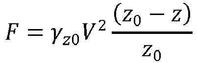
- the levitation force acts in the opposite direction as the parallel plate force and shows inverse non-linear behavior. By combining both of these forces, a linear out-of-plane actuator can be implemented.
- the levitation force is a non-linear force that depends on in-plane deflection ( x ), out-of-plane deflection ( z ), and applied voltage (V).
- the parameters of the levitation force are defined by geometry of the drive comb (overlap, gap between proof mass, and dimension of drive comb fingers).
- the parallel plate force is a non-linear force that depends on out-of-plane deflection, applied voltage, gap between the structure and the plate, and depends on in-plane deflection if the area of the parallel plate is designed such that it changes over in-plane motion.
- the force dependence on x and/or z is undesirable in most cases. Therefore, the present actuator uses such arrangement and combination of both levitation and parallel plate forces to arrive at a force that acts out-of-plane and which depends only on applied voltage.
- the parallel plate sense electrodes have constant area or are designed such that the sum of area of both electrodes is constant, there is no force acting in-plane. Linearization of the parallel plate and combining the linearized force with levitation, and realizing that both forces act in opposite directions, a specific condition is obtained. If the design fulfills such condition, a linear actuator can be achieved. The extent to which the force is linear depends on the design of both the drive comb and parallel plate actuator, and the out-of-plane displacement.
- the present linear out-of-plane actuator allows for higher yield and/or higher performance MEMS inertial sensors to be produced.
- the linear out-of-plane actuator can be also used to improve the dynamics of MEMS inertial sensors by using the actuator in a force feedback loop.
- the present approach is particularly suited for use in high performance MEMS inertial sensors, such as MEMS accelerometers and MEMS gyroscopes, which are manufactured by single sided manufacturing technologies.
- the present technique can be used to reduce vibration sensitivity of single sense plate gyroscopes and accelerometers using levitation and parallel plate actuators.
- the drive comb of a MEMS device includes two sets of electrodes with interdigitated comb fingers.
- One set of electrodes is fixed to a substrate (static) and the other set of electrodes is movable.
- the electrostatic force drives the movable set of electrodes towards the static set of electrodes.
- a symmetrical drive comb with both static and movable drive comb electrodes having the same thickness, can be used for in-plane and small out-of-plane movement.
- Such a symmetrical drive comb has the advantage that the in-plane force is independent of deflection. Strictly speaking, the force is constant if the capacitance is linearly proportional to the displacement. Consequently, the drive comb is linear only when the motion is within the overlap of about 10% or greater. When the motion reaches 0% of overlap, the fringe capacitance (edges of comb fingers) start to dominate and therefore the entire capacitance does not depend linearly on displacement and the force is non-linear. However, a linear range can be designed by using comb fingers with adequate length.
- the drive comb is the actuator of choice for many devices since the drive comb offers linear scaling with applied voltage and allows for large displacement.
- FIG. 1A illustrates a conventional drive comb 10 that can be employed in a MEMS sensor device, for example.
- the drive comb 10 includes a fixed electrode 20 having a first set of comb fingers 22, and a movable electrode 30 having a second set of comb fingers 32.
- the first and second sets of comb fingers 22, 32 face each other in an interdigitated configuration.
- the fixed electrode 20 and the movable electrode 30 have the same height (H 0 ), and are positioned with respect to each other such that a comb finger spacing (D 0 ) exists between each interdigitated comb finger 22, 32 in an x direction.
- a comb finger overlap (Y 0 ) exists between each interdigitated comb finger 22, 32 in the y direction.
- the movable electrode 30 can travel back and forth along the y direction as indicated by arrow 40.
- a voltage (V) applied at electrical connection 50 provides the electrostatic force that drives movable electrode 30 towards fixed electrode 20.
- the force ( F ) along the y direction is defined as a partial derivative along that direction multiplied by 1 2 V 2 .
- the size and direction of the force acting in-plane for drive comb 10 is shown in the diagram of Figure 1B , with the fixed structure corresponding to fixed electrode 20, and the movable structure corresponding to movable electrode 30.
- the dashed lines indicate the original position of moveable electrode 30.
- the drive comb structure can be driven by either DC + AC voltage at frequency ⁇ or AC only at frequency 2 ⁇ .
- sinusoidal/periodic motion typically for MEMS gyroscopes, the voltage is varied by AC value at the resonant frequency and the movable structure is pushed towards the static structure.
- the force is independent of displacement of the movable structures in the y direction, and can achieve a large displacement limited only by the length of the comb fingers.
- the actuator in a perpendicular direction can be implemented enabling both directional actuation in the x and y directions independent of displacement.
- the problematic part is the actuation in the out-of-plane direction, where the drive comb cannot be used in the way it is in the in-plane direction.
- An out-of-plane actuator can be implemented by a parallel plate, or by a drive comb of a MEMS device. Based on the type of drive comb, and whether or not there is symmetry beneath and above the drive comb, two forces can be distinguished. For a symmetrical drive comb, there is the force that always tries to push the movable part towards the static part. This is described by the equation in Table 1 above (Z direction). For a non-symmetrical drive comb (single sided technology), there is the levitation force, which always pushes the movable part above the static part (makes it levitate). The substrate (silicon or electrode below the drive comb) is typically grounded for the non-symmetrical drive comb.
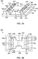
- FIGS 3A-3D illustrate a MEMS sensor device 100 according to one embodiment, to which the present approach can be applied.
- the MEMS sensor device 100 generally includes a support substrate 104, and a proof mass 110 movably connected to substrate 104.
- a first drive comb 120 and a second drive comb 130 are oppositely oriented on either side of proof mass 110 and are fixedly connected to substrate 104.
- a parallel plate sense electrode 140 is located under proof mass 110 on substrate 104.
- the proof mass 110 is configured to oscillate back and forth over support substrate 104 between drive combs 120 and 130, both of which remain stationary over substrate 104 to limit movement of proof mass 110. Extending outwardly from opposing ends of proof mass 110 are a first set of comb fingers 112 and a second set of comb fingers 114, which are used to electrostatically drive proof mass 110.
- the first drive comb 120 has a first set of comb fingers 122, which can be interdigitated with the first set of comb fingers 112 on proof mass 110.
- the second drive comb 130 has a second set of comb fingers 132, which can be interdigitated with the second set of comb fingers 114 on proof mass 110.
- MEMS device 100 can be connected to substrate 104 through various suspension structures (not shown).
- the parallel plate sense electrode 140 can include a rectangular-shaped electrode plate positioned and oriented in a manner such that an upper face of parallel plate sense electrode 140 is vertically adjacent to and parallel with the underside of proof mass 110.
- the drive comb is divided into two parts such that the overlap is always constant, and parallel plate sense electrode 140 is entirely beneath proof mass 110.
- the levitation force occurs when there is nonsymmetrical electrical field as a result of a plate beneath the substrate, which is biased at the same voltage.
- ⁇ Z 0 is linked to the design of the comb and describes the ratio between force and square of applied voltage for specific overlap.
- the unit of ⁇ Z 0 is N / V 2 and a typical value is in the range of fraction of nN per V 2 .
- the parameter z 0 is the equilibrium position. The equilibrium position defines the maximal displacement that can be achieved by the levitation force. If there is no mechanical restoring spring constant, the structure would always levitate at Z 0 .
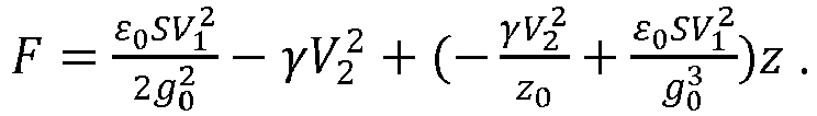
- F ⁇ V 2 ⁇ ⁇ V 2 z 0 z
- This equation describes the force acting on the structure when there is only one parallel plate (one sided technology).
- this equation has two terms:
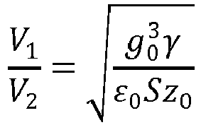
- V 1 V 2 g 0 3 ⁇ ⁇ 0 Sz 0
- the independent term of displacement for this linear actuator ⁇ 0 SV 2 2 g 0 2 ⁇ ⁇ V 2 implies that both forces act in opposite directions.
- FIG 4A The combination of the levitation force with the parallel plate force is illustrated in Figure 4A for a MEMS sensor device 200 similar to that shown in Figures 3A-3D .
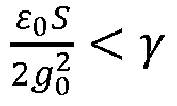
- the levitation force is larger corresponding to ⁇ 0 SV 2 2 g 0 2 ⁇ ⁇ or g 0 2 z 0 ⁇ 1 condition, so the linearized force points upward.
- the combination of the levitation force with the parallel plate force is also illustrated in Figure 4B for MEMS sensor device 200.
- the parallel plate force is larger, corresponding to ⁇ 0 S 2 g 0 2 > ⁇ or g 0 2 z 0 > 1 condition, so the linearized force points downward.
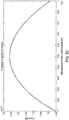
- Figure 5A shows the linearity of levitation force within 100 nm of displacement in the z axis from the initial position.
- Figure 5B shows the linearity of parallel plate force within 100 nm of displacement in the z axis from the initial position.
- Figure 5C shows the linearity of combined levitation and parallel plate forces, within 100 nm of displacement in the z axis from the initial position.
- the force is independent of in-plane motion.
- the dependence on in-plane deflection is apparent from equations (both the area of the parallel plate and overlap of the drive comb depends on in-plane motion), which makes both forces dependent on y deflection.
- the geometry is designed such that the plate and/or the overlap does not change (or rather sum of several drive combs), the force is independent of displacement.
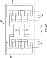
- FIG. 6 illustrates a MEMS sensor device 300 according to another embodiment, to which the present approach can be applied.
- the MEMS sensor device 300 includes a support substrate 304, and a proof mass 310 movably connected to substrate 304.
- a first pair of drive combs 320, 322 with opposite orientations (A and B), and a second pair of drive combs 330, 332 with an opposite orientations (A and B), are both fixedly connected to substrate 304.
- a pair of parallel plate sense electrodes 340, 344 is located under proof mass 310 on substrate 304.
- the proof mass 310 is configured to move back and forth in-plane over support substrate 304 as indicated by arrow 350.
- the first pair of drive combs 320, 322 each include comb fingers, which can be interdigitated with adjacent comb fingers of proof mass 310.
- the second pair of drive combs 330, 332 each include comb fingers, which can be interdigitated with adjacent comb fingers of proof mass 310.
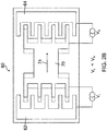
- FIG. 7 illustrates a MEMS sensor device 400 according to an alternative embodiment, to which the present approach can be applied.
- the MEMS sensor device 400 includes a support substrate 404, and a proof mass 410 movably connected to substrate 404.
- a first pair of drive combs 420, 422 with opposite orientations (A and B), and a second pair of drive combs 430, 432 with opposite orientations (A and B), are both fixedly connected to substrate 404.
- a first pair of parallel plate sense electrodes 440, 444 is located under proof mass 410 on substrate 404 in an overlapping arrangement with drive combs 420, 422.
- a second pair of parallel plate sense electrodes 450, 454 is located under proof mass 410 on substrate 404 in an overlapping arrangement with drive combs 430, 432.
- the proof mass 410 is configured to move back and forth in-plane over support substrate 404 as indicated by arrow 460.
- the first pair of drive combs 420, 422 each include comb fingers, which can be interdigitated with adjacent comb fingers of proof mass 410.
- the second pair of drive combs 430, 432 each include comb fingers, which can be interdigitated with adjacent comb fingers of proof mass 410.
- the drive combs with opposite orientations With the drive combs with opposite orientations with the same voltages in the MEMS sensor devices, and the fact that the in-plane force is independent of displacement, the sum of force for the in-plane motion is zero.
- the forces for the drive combs with opposite orientations should have both DC and AC components, which have opposite signs in order to decrease electrical feedthrough.
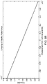
- Figure 8 is a graph showing experimental verification of control of motion demonstrated as an active damping of out-of-plane mode for a MEMS structure when both actuators with different voltage ratios were used.
- Figure 8 shows movement control for a levitation and parallel plate combination, with the amplitude (out-of-plane displacement) being a function of frequency. This shows that active damping with the proposed actuator could achieve adjustment of damping by a factor of ten.
Landscapes
- Physics & Mathematics (AREA)
- Engineering & Computer Science (AREA)
- General Physics & Mathematics (AREA)
- Radar, Positioning & Navigation (AREA)
- Remote Sensing (AREA)
- Micromachines (AREA)
Description
- When micro-electro-mechanical systems (MEMS) devices such as MEMS inertial sensors are subject to external forces such as vibration, functionality may be lost and/or performance may be compromised. There have been various approaches to address how to reduce vibration of MEMS sensors.
- In one prior approach, a comb drive was used to create an out-of-plane force to reduce vibration in a MEMS device. This approach is based on using a fringe field of the comb drive, which does not have a substrate beneath. Consequently, this approach is not usable for devices that do have electrodes beneath the comb drive (e.g., out-of-plane accelerometer and in-plane gyroscope). Moreover, the force produced is non-linear around zero deflection since it depends on displacement out-of-plane.
- In another prior approach, a method for quadrature reduction in MEMS gyroscope devices uses a set of parallel plate electrodes to compensate for quadrature movement. However, using such electrodes to compensate motion out-of-plane results in a non-linear force, and if a DC bias is used, a change of resonant frequency. Moreover, a parallel plate actuator in unstable for higher actuation voltages.
- Document "Electrostatic comb drive levitation and control method" (Journal of Microelectromechanical Systems, vol. 1, ) discloses a method for reducing the levitation force using the force induced by a trapped charge in a silicon nitride passivation layer.
- While MEMS gyroscopes generally provide good angle random walk (ARW), robustness against severe shocks and vibration, and bias stability for certain applications, is inadequate. The reduction of bias can be achieved by improving the manufacturing process, by solving the problem at the system level, such as adding in-run calibration or by compensating the movement with electrostatic actuators. Nevertheless, the actuation in out-of-plane direction is more complicated as opposed to in-plane, since out-of-plane actuators based on parallel plate electrodes are inherently non-linear. Moreover, if single sided manufacturing technology is used, parallel plate force can act only in one direction. The in-plane actuation is less complicated due to the possibility to use drive combs which are linear actuators.
- Accordingly, there is a need to actuate MEMS devices in an out-of-plane direction by a linear force, which is independent of both in-plane and out-of-plane displacement.
- A MEMS sensor device comprises a support substrate, a proof mass movably connected to the support substrate, a first drive comb fixedly connected to the support substrate in a first orientation and adjacent to the proof mass, and a second drive comb fixedly connected to the support substrate in a second orientation and adjacent to the proof mass. The second orientation is opposite of the first orientation such that the first and second drive combs face toward each other. A parallel plate sense electrode is located under the proof mass on the support substrate. The first and second drive combs, and the parallel plate sense electrode, are each electrically charged and configured with respect to the proof mass such that a combination of a levitation force and a parallel plate force produces a linear out-of-plane actuation for the MEMS sensor device that depends only on an applied voltage.
- Features of the present invention will become apparent to those skilled in the art from the following description with reference to the drawings. Understanding that the drawings depict only typical embodiments and are not therefore to be considered limiting in scope, the invention will be described with additional specificity and detail through the use of the accompanying drawings, in which:
-
Figure 1A is an isometric view of a conventional drive comb that can be employed in a MEMS device; -
Figure 1B is a diagram of the size and direction of the force acting in-plane on moveable structures of the drive comb ofFigure 1A ; -
Figures 2A and2B are schematic diagrams of a MEMS device, which show the opposing forces acting on a moveable structure of the MEMS device; -
Figure 3A is an isometric view of a micro-electro-mechanical systems (MEMS) sensor device according to one embodiment, which can be implemented as an out of plane actuator; -
Figure 3B is a top view of the MEMS sensor device shown inFigure 3A ; -
Figure 3C is a front view of the MEMS sensor device shown inFigure 3A ; -
Figure 3D is a cross-sectional side view of the MEMS sensor device shown inFigure 3B taken along line 3D-3D; -
Figures 4A and4B show cross-sectional side views of a MEMS sensor device, showing the combination of levitation and parallel plate forces acting on the MEMS sensor device; -
Figure 5A is a graph of linearity for the levitation force, with respect to displacement along the z axis; -
Figure 5B is a graph of linearity for the parallel plate force, with respect to displacement along the z axis; -
Figure 5C is a graph showing the combined levitation and parallel plate forces, with respect to displacement along the z axis; -
Figure 6 is a top view of a MEMS sensor device according to another embodiment, which can be implemented as an out of plane actuator; -
Figure 7 is a top view of a MEMS sensor device according to an alternative embodiment, which can be implemented as an out of plane actuator; and -
Figure 8 is a graph showing experimental verification of control of motion demonstrated as an active damping of out-of-plane mode for a MEMS structure. - In the following detailed description, embodiments are described in sufficient detail to enable those skilled in the art to practice the invention. It is to be understood that other embodiments may be utilized without departing from the scope of the invention. The following detailed description is, therefore, not to be taken in a limiting sense.
- A micro-electro-mechanical systems (MEMS) out-of-plane actuator for MEMS devices is disclosed herein that is configured to use a combination of a parallel plate force and a levitation force. The levitation force acts in the opposite direction as the parallel plate force and shows inverse non-linear behavior. By combining both of these forces, a linear out-of-plane actuator can be implemented.
- The levitation force is a non-linear force that depends on in-plane deflection (x), out-of-plane deflection (z), and applied voltage (V). The parameters of the levitation force are defined by geometry of the drive comb (overlap, gap between proof mass, and dimension of drive comb fingers). The parallel plate force is a non-linear force that depends on out-of-plane deflection, applied voltage, gap between the structure and the plate, and depends on in-plane deflection if the area of the parallel plate is designed such that it changes over in-plane motion. The force dependence on x and/or z is undesirable in most cases. Therefore, the present actuator uses such arrangement and combination of both levitation and parallel plate forces to arrive at a force that acts out-of-plane and which depends only on applied voltage.
- If the parallel plate sense electrodes have constant area or are designed such that the sum of area of both electrodes is constant, there is no force acting in-plane. Linearization of the parallel plate and combining the linearized force with levitation, and realizing that both forces act in opposite directions, a specific condition is obtained. If the design fulfills such condition, a linear actuator can be achieved. The extent to which the force is linear depends on the design of both the drive comb and parallel plate actuator, and the out-of-plane displacement.
- The present linear out-of-plane actuator allows for higher yield and/or higher performance MEMS inertial sensors to be produced. The linear out-of-plane actuator can be also used to improve the dynamics of MEMS inertial sensors by using the actuator in a force feedback loop.
- The present approach is particularly suited for use in high performance MEMS inertial sensors, such as MEMS accelerometers and MEMS gyroscopes, which are manufactured by single sided manufacturing technologies. The present technique can be used to reduce vibration sensitivity of single sense plate gyroscopes and accelerometers using levitation and parallel plate actuators.
- Further details of the present approach are described hereafter with reference to the drawings.
- The drive comb of a MEMS device includes two sets of electrodes with interdigitated comb fingers. One set of electrodes is fixed to a substrate (static) and the other set of electrodes is movable. When a voltage is applied between the electrodes, the electrostatic force drives the movable set of electrodes towards the static set of electrodes.
- A symmetrical drive comb, with both static and movable drive comb electrodes having the same thickness, can be used for in-plane and small out-of-plane movement. Such a symmetrical drive comb has the advantage that the in-plane force is independent of deflection. Strictly speaking, the force is constant if the capacitance is linearly proportional to the displacement. Consequently, the drive comb is linear only when the motion is within the overlap of about 10% or greater. When the motion reaches 0% of overlap, the fringe capacitance (edges of comb fingers) start to dominate and therefore the entire capacitance does not depend linearly on displacement and the force is non-linear. However, a linear range can be designed by using comb fingers with adequate length. The drive comb is the actuator of choice for many devices since the drive comb offers linear scaling with applied voltage and allows for large displacement.
-
Figure 1A illustrates aconventional drive comb 10 that can be employed in a MEMS sensor device, for example. Thedrive comb 10 includes a fixedelectrode 20 having a first set ofcomb fingers 22, and amovable electrode 30 having a second set ofcomb fingers 32. The first and second sets ofcomb fingers electrode 20 and themovable electrode 30 have the same height (H0), and are positioned with respect to each other such that a comb finger spacing (D0) exists between eachinterdigitated comb finger interdigitated comb finger movable electrode 30 can travel back and forth along the y direction as indicated byarrow 40. A voltage (V) applied atelectrical connection 50 provides the electrostatic force that drivesmovable electrode 30 towards fixedelectrode 20. - The capacitance (C) of
drive comb 10 can be described by the following equation:
- The force (F) along the y direction is defined as a partial derivative along that direction multiplied by


- The forces in
drive comb 10 ofFigure 1A can therefore be described as follows in Table 1.Table 1 Direction Force Notes Y 
Force independent of displacement in y direction; scales with voltage square; always attracts movable towards static part. Z 
Valid when there is no substrate beneath. Force depends on displacement but only for small z; for larger z, force independent of z; there is no force if there is no deflection. X 
Force depends on displacement (x); force may cause collapse of the structure since when x increases (fingers approach each other) → force increases; this force is balanced (x = 0) and therefore force = 0 mostly. - The size and direction of the force acting in-plane for
drive comb 10 is shown in the diagram ofFigure 1B , with the fixed structure corresponding to fixedelectrode 20, and the movable structure corresponding tomovable electrode 30. The dashed lines indicate the original position ofmoveable electrode 30. - In the use of voltage to drive the structure of
drive comb 10, force is defined as:

Figures 2A and2B for aMEMS device 60, where a pair of fixeddrive comb electrodes moveable electrode 70. A voltage (VL) is applied on the left side ofMEMS device 60 betweendrive comb electrode 62 andmoveable electrode 70, and a voltage (VR) is applied on the right side ofMEMS device 60 betweendrive comb electrode 64 andmoveable electrode 70. As depicted inFigure 2A , when VL is greater than VR, a force indicated byarrow 72 drivesmovable electrode 70 towarddrive comb electrode 62. As depicted inFigure 2B , when VL is less than VR, a force indicated byarrow 74 drivesmovable electrode 70 towarddrive comb electrode 64. - Accordingly, the force is independent of displacement of the movable structures in the y direction, and can achieve a large displacement limited only by the length of the comb fingers. By rotating the actuator by 90 degrees, the actuator in a perpendicular direction can be implemented enabling both directional actuation in the x and y directions independent of displacement. The problematic part is the actuation in the out-of-plane direction, where the drive comb cannot be used in the way it is in the in-plane direction.
- An out-of-plane actuator can be implemented by a parallel plate, or by a drive comb of a MEMS device. Based on the type of drive comb, and whether or not there is symmetry beneath and above the drive comb, two forces can be distinguished. For a symmetrical drive comb, there is the force that always tries to push the movable part towards the static part. This is described by the equation in Table 1 above (Z direction). For a non-symmetrical drive comb (single sided technology), there is the levitation force, which always pushes the movable part above the static part (makes it levitate). The substrate (silicon or electrode below the drive comb) is typically grounded for the non-symmetrical drive comb.
-
Figures 3A-3D illustrate aMEMS sensor device 100 according to one embodiment, to which the present approach can be applied. TheMEMS sensor device 100 generally includes asupport substrate 104, and aproof mass 110 movably connected tosubstrate 104. Afirst drive comb 120 and asecond drive comb 130 are oppositely oriented on either side ofproof mass 110 and are fixedly connected tosubstrate 104. A parallelplate sense electrode 140 is located underproof mass 110 onsubstrate 104. - The
proof mass 110 is configured to oscillate back and forth oversupport substrate 104 between drive combs 120 and 130, both of which remain stationary oversubstrate 104 to limit movement ofproof mass 110. Extending outwardly from opposing ends ofproof mass 110 are a first set ofcomb fingers 112 and a second set ofcomb fingers 114, which are used to electrostatically driveproof mass 110. - The
first drive comb 120 has a first set ofcomb fingers 122, which can be interdigitated with the first set ofcomb fingers 112 onproof mass 110. Likewise, thesecond drive comb 130 has a second set ofcomb fingers 132, which can be interdigitated with the second set ofcomb fingers 114 onproof mass 110. - The foregoing components of
MEMS device 100 can be connected tosubstrate 104 through various suspension structures (not shown). - The parallel
plate sense electrode 140 can include a rectangular-shaped electrode plate positioned and oriented in a manner such that an upper face of parallelplate sense electrode 140 is vertically adjacent to and parallel with the underside ofproof mass 110. In the implementation shown, the drive comb is divided into two parts such that the overlap is always constant, and parallelplate sense electrode 140 is entirely beneathproof mass 110. - The levitation force occurs when there is nonsymmetrical electrical field as a result of a plate beneath the substrate, which is biased at the same voltage. The levitation force is described by the following equation:


- The force as a linear function of displacement is defined by:

- The parallel plate force is defined by:
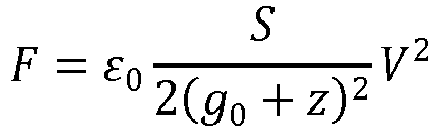


- 1) a term independent of displacement, where force is a function of geometry and applied voltage; and
- 2) a term that linearly depends on displacement and where the force is a function of geometry and applied voltage.
- Combining the equation for the parallel
plate force 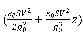
levitation force 


linear actuator 

linearization 

condition 

- The combination of the levitation force with the parallel plate force is illustrated in
Figure 4A for a MEMS sensor device 200 similar to that shown inFigures 3A-3D . In this case, the levitation force is larger corresponding to

- The combination of the levitation force with the parallel plate force is also illustrated in
Figure 4B for MEMS sensor device 200. In this case, the parallel plate force is larger, corresponding to

- When the condition for linearization is fulfilled, a force can be obtained as shown in the graphs of
Figures 5A-5C .Figure 5A shows the linearity of levitation force within 100 nm of displacement in the z axis from the initial position.Figure 5B shows the linearity of parallel plate force within 100 nm of displacement in the z axis from the initial position.Figure 5C shows the linearity of combined levitation and parallel plate forces, within 100 nm of displacement in the z axis from the initial position. - Furthermore, if the actuator is designed such that the area is constant with respect to in-plane movement, the force is independent of in-plane motion. The dependence on in-plane deflection is apparent from equations (both the area of the parallel plate and overlap of the drive comb depends on in-plane motion), which makes both forces dependent on y deflection. The parallel plate depends on in-plane deflection as follows:


-
Figure 6 illustrates aMEMS sensor device 300 according to another embodiment, to which the present approach can be applied. TheMEMS sensor device 300 includes asupport substrate 304, and aproof mass 310 movably connected tosubstrate 304. A first pair of drive combs 320, 322 with opposite orientations (A and B), and a second pair of drive combs 330, 332 with an opposite orientations (A and B), are both fixedly connected tosubstrate 304. A pair of parallelplate sense electrodes proof mass 310 onsubstrate 304. - The
proof mass 310 is configured to move back and forth in-plane oversupport substrate 304 as indicated byarrow 350. The first pair of drive combs 320, 322 each include comb fingers, which can be interdigitated with adjacent comb fingers ofproof mass 310. Likewise, the second pair of drive combs 330, 332 each include comb fingers, which can be interdigitated with adjacent comb fingers ofproof mass 310. -
Figure 7 illustrates aMEMS sensor device 400 according to an alternative embodiment, to which the present approach can be applied. TheMEMS sensor device 400 includes asupport substrate 404, and aproof mass 410 movably connected tosubstrate 404. A first pair of drive combs 420, 422 with opposite orientations (A and B), and a second pair of drive combs 430, 432 with opposite orientations (A and B), are both fixedly connected tosubstrate 404. A first pair of parallelplate sense electrodes proof mass 410 onsubstrate 404 in an overlapping arrangement with drive combs 420, 422. A second pair of parallelplate sense electrodes proof mass 410 onsubstrate 404 in an overlapping arrangement with drive combs 430, 432. - The
proof mass 410 is configured to move back and forth in-plane oversupport substrate 404 as indicated byarrow 460. The first pair of drive combs 420, 422 each include comb fingers, which can be interdigitated with adjacent comb fingers ofproof mass 410. Likewise, the second pair of drive combs 430, 432 each include comb fingers, which can be interdigitated with adjacent comb fingers ofproof mass 410. - By using the drive combs with opposite orientations with the same voltages in the MEMS sensor devices, and the fact that the in-plane force is independent of displacement, the sum of force for the in-plane motion is zero. The forces for the drive combs with opposite orientations should have both DC and AC components, which have opposite signs in order to decrease electrical feedthrough.
-
Figure 8 is a graph showing experimental verification of control of motion demonstrated as an active damping of out-of-plane mode for a MEMS structure when both actuators with different voltage ratios were used.Figure 8 shows movement control for a levitation and parallel plate combination, with the amplitude (out-of-plane displacement) being a function of frequency. This shows that active damping with the proposed actuator could achieve adjustment of damping by a factor of ten.
Claims (10)
- A MEMS sensor device (100, 300, 400), comprising:a support substrate (104, 304, 404);a proof mass (110, 310, 410) movably connected to the support substrate;a first drive comb (120, 320, 332, 420, 432) fixedly connected to the support substrate in a first orientation and adjacent to the proof mass;a second drive comb (130, 322, 330, 422, 430) fixedly connected to the support substrate in a second orientation and adjacent to the proof mass, the second orientation opposite of the first orientation such that the first and second drive combs face toward each other; anda parallel plate sense electrode (140, 340, 344, 440, 444, 450, 454) located under the proof mass on the support substrate;wherein the first and second drive combs, and the parallel plate sense electrode, are each electrically charged and configured with respect to the proof mass such that a combination of a levitation force and a parallel plate force produces a force substantially independent of displacement along a z-axis for out-of-plane actuation for the MEMS sensor device that depends only on an applied voltage, thereby producing a vibration reduction of the MEMS sensor device.
- The MEMS sensor device of claim 1, wherein the drive combs are divided into two parts such that an overlap between the proof mass, and the first and second drive combs, is constant.
- The MEMS sensor device of claim 2, wherein the parallel plate sense electrode is entirely beneath the proof mass.
- The MEMS sensor device of claim 2, wherein the parallel plate sense electrode is located adjacent to the overlap.
- The MEMS sensor device of claim 1, wherein the MEMS sensor device comprises a MEMS inertial sensor.
- The MEMS sensor device of claim 1, wherein the applied voltage comprises a DC signal, an AC signal, or combinations thereof.
- The MEMS sensor device of claim 3, wherein the applied voltage is a single voltage.
- The MEMS sensor device of claim 7, wherein the MEMS sensor device has a geometric configuration defined by the equation:

- The MEMS sensor device of claim 1, wherein the applied voltage comprises a first voltage applied to the parallel plate sense electrode, and a second voltage applied to the drive combs, the second voltage being different from the first voltage.
- The MEMS sensor device of claim 3, wherein the applied voltage comprises a fixed ratio of voltages defined by:

Applications Claiming Priority (1)
| Application Number | Priority Date | Filing Date | Title |
|---|---|---|---|
| US201715459293 | 2017-03-15 |
Publications (2)
| Publication Number | Publication Date |
|---|---|
| EP3376162A1 EP3376162A1 (en) | 2018-09-19 |
| EP3376162B1 true EP3376162B1 (en) | 2019-11-20 |
Family
ID=61627016
Family Applications (1)
| Application Number | Title | Priority Date | Filing Date |
|---|---|---|---|
| EP18161335.7A Active EP3376162B1 (en) | 2017-03-15 | 2018-03-12 | Mems out of plane actuator |
Country Status (1)
| Country | Link |
|---|---|
| EP (1) | EP3376162B1 (en) |
Families Citing this family (2)
| Publication number | Priority date | Publication date | Assignee | Title |
|---|---|---|---|---|
| CN112113553B (en) * | 2020-09-15 | 2022-06-21 | 浙江大学 | Gyro full-matching tuning electrode |
| CN114414848B (en) * | 2021-12-01 | 2022-10-25 | 西安电子科技大学 | Feed-through capacitance extraction method of MEMS capacitive sensor based on symmetric driving |
Citations (1)
| Publication number | Priority date | Publication date | Assignee | Title |
|---|---|---|---|---|
| US20140144231A1 (en) * | 2012-11-28 | 2014-05-29 | Freescale Semiconductor, Inc. | Inertial sensor and method of levitation effect compensation |
-
2018
- 2018-03-12 EP EP18161335.7A patent/EP3376162B1/en active Active
Patent Citations (1)
| Publication number | Priority date | Publication date | Assignee | Title |
|---|---|---|---|---|
| US20140144231A1 (en) * | 2012-11-28 | 2014-05-29 | Freescale Semiconductor, Inc. | Inertial sensor and method of levitation effect compensation |
Non-Patent Citations (1)
| Title |
|---|
| TANG W C ET AL: "Electrostatically balanced comb drive for controlled levitation", SOLID-STATE SENSOR AND ACTUATOR WORKSHOP, 1990. 4TH TECHNICAL DIGEST., IEEE, IEEE, 4 June 1990 (1990-06-04), pages 23 - 27, XP032355739, DOI: 10.1109/SOLSEN.1990.109812 * |
Also Published As
| Publication number | Publication date |
|---|---|
| EP3376162A1 (en) | 2018-09-19 |
Similar Documents
| Publication | Publication Date | Title |
|---|---|---|
| US7036373B2 (en) | MEMS gyroscope with horizontally oriented drive electrodes | |
| EP2071284B1 (en) | Parametric amplification of a MEMS gyroscope by capacitance modulation | |
| EP1603830B1 (en) | An accelerometer | |
| JP3039364B2 (en) | Angular velocity sensor | |
| EP2419370B1 (en) | Long travel range mems actuator | |
| US7279761B2 (en) | Post-release capacitance enhancement in micromachined devices and a method of performing the same | |
| US10753744B2 (en) | MEMS out of plane actuator | |
| US20160356806A1 (en) | Accelerometers | |
| KR102095475B1 (en) | Accelerometer | |
| WO2003031912A2 (en) | Tuning fork gyroscope | |
| KR100373484B1 (en) | vibrating micromachined gyroscope | |
| US20160153781A1 (en) | Quadrature compensation | |
| JP2018514397A (en) | Structure and device of microelectromechanical capacitive sensor | |
| US6536280B1 (en) | Thin film MEMS sensors employing electrical sensing and force feedback | |
| EP3376162B1 (en) | Mems out of plane actuator | |
| JP2004340716A (en) | Acceleration sensor | |
| US20160101975A1 (en) | Resonance Frequency Adjustment Module | |
| JP2000055670A (en) | Vibration detector | |
| US7267005B1 (en) | SOI-MEMS gyroscope having three-fold symmetry | |
| EP2570770B1 (en) | Three-mass coupled oscillation technique for mechanically robust micromachined gyroscopes | |
| US7308827B2 (en) | Integrated gyroscope and temperature sensor | |
| US20070267939A1 (en) | Systems and methods for improved control of micro-electrical-mechanical system (MEMS) electrostatic actuator | |
| Del Corro et al. | Comb drive designs with minimized levitation | |
| JP4320934B2 (en) | Semiconductor angular velocity sensor | |
| US20140283606A1 (en) | Acceleration sensor |
Legal Events
| Date | Code | Title | Description |
|---|---|---|---|
| PUAI | Public reference made under article 153(3) epc to a published international application that has entered the european phase |
Free format text: ORIGINAL CODE: 0009012 |
|
| STAA | Information on the status of an ep patent application or granted ep patent |
Free format text: STATUS: REQUEST FOR EXAMINATION WAS MADE |
|
| 17P | Request for examination filed |
Effective date: 20180312 |
|
| AK | Designated contracting states |
Kind code of ref document: A1 Designated state(s): AL AT BE BG CH CY CZ DE DK EE ES FI FR GB GR HR HU IE IS IT LI LT LU LV MC MK MT NL NO PL PT RO RS SE SI SK SM TR |
|
| AX | Request for extension of the european patent |
Extension state: BA ME |
|
| GRAP | Despatch of communication of intention to grant a patent |
Free format text: ORIGINAL CODE: EPIDOSNIGR1 |
|
| STAA | Information on the status of an ep patent application or granted ep patent |
Free format text: STATUS: GRANT OF PATENT IS INTENDED |
|
| INTG | Intention to grant announced |
Effective date: 20190711 |
|
| RIN1 | Information on inventor provided before grant (corrected) |
Inventor name: KRAUSOVA, HANA Inventor name: JANDAK, MIKULAS Inventor name: SCHMIDT, ULRICH Inventor name: SCHNEIDER, MICHAEL Inventor name: NEUZIL, TOMAS |
|
| GRAA | (expected) grant |
Free format text: ORIGINAL CODE: 0009210 |
|
| STAA | Information on the status of an ep patent application or granted ep patent |
Free format text: STATUS: THE PATENT HAS BEEN GRANTED |
|
| GRAS | Grant fee paid |
Free format text: ORIGINAL CODE: EPIDOSNIGR3 |
|
| AK | Designated contracting states |
Kind code of ref document: B1 Designated state(s): AL AT BE BG CH CY CZ DE DK EE ES FI FR GB GR HR HU IE IS IT LI LT LU LV MC MK MT NL NO PL PT RO RS SE SI SK SM TR |
|
| REG | Reference to a national code |
Ref country code: GB Ref legal event code: FG4D |
|
| REG | Reference to a national code |
Ref country code: CH Ref legal event code: EP |
|
| REG | Reference to a national code |
Ref country code: IE Ref legal event code: FG4D |
|
| REG | Reference to a national code |
Ref country code: DE Ref legal event code: R096 Ref document number: 602018001214 Country of ref document: DE |
|
| REG | Reference to a national code |
Ref country code: AT Ref legal event code: REF Ref document number: 1204679 Country of ref document: AT Kind code of ref document: T Effective date: 20191215 |
|
| REG | Reference to a national code |
Ref country code: NL Ref legal event code: MP Effective date: 20191120 |
|
| REG | Reference to a national code |
Ref country code: LT Ref legal event code: MG4D |
|
| PG25 | Lapsed in a contracting state [announced via postgrant information from national office to epo] |
Ref country code: SE Free format text: LAPSE BECAUSE OF FAILURE TO SUBMIT A TRANSLATION OF THE DESCRIPTION OR TO PAY THE FEE WITHIN THE PRESCRIBED TIME-LIMIT Effective date: 20191120 Ref country code: LV Free format text: LAPSE BECAUSE OF FAILURE TO SUBMIT A TRANSLATION OF THE DESCRIPTION OR TO PAY THE FEE WITHIN THE PRESCRIBED TIME-LIMIT Effective date: 20191120 Ref country code: GR Free format text: LAPSE BECAUSE OF FAILURE TO SUBMIT A TRANSLATION OF THE DESCRIPTION OR TO PAY THE FEE WITHIN THE PRESCRIBED TIME-LIMIT Effective date: 20200221 Ref country code: NO Free format text: LAPSE BECAUSE OF FAILURE TO SUBMIT A TRANSLATION OF THE DESCRIPTION OR TO PAY THE FEE WITHIN THE PRESCRIBED TIME-LIMIT Effective date: 20200220 Ref country code: FI Free format text: LAPSE BECAUSE OF FAILURE TO SUBMIT A TRANSLATION OF THE DESCRIPTION OR TO PAY THE FEE WITHIN THE PRESCRIBED TIME-LIMIT Effective date: 20191120 Ref country code: BG Free format text: LAPSE BECAUSE OF FAILURE TO SUBMIT A TRANSLATION OF THE DESCRIPTION OR TO PAY THE FEE WITHIN THE PRESCRIBED TIME-LIMIT Effective date: 20200220 Ref country code: LT Free format text: LAPSE BECAUSE OF FAILURE TO SUBMIT A TRANSLATION OF THE DESCRIPTION OR TO PAY THE FEE WITHIN THE PRESCRIBED TIME-LIMIT Effective date: 20191120 Ref country code: NL Free format text: LAPSE BECAUSE OF FAILURE TO SUBMIT A TRANSLATION OF THE DESCRIPTION OR TO PAY THE FEE WITHIN THE PRESCRIBED TIME-LIMIT Effective date: 20191120 |
|
| PG25 | Lapsed in a contracting state [announced via postgrant information from national office to epo] |
Ref country code: IS Free format text: LAPSE BECAUSE OF FAILURE TO SUBMIT A TRANSLATION OF THE DESCRIPTION OR TO PAY THE FEE WITHIN THE PRESCRIBED TIME-LIMIT Effective date: 20200320 Ref country code: HR Free format text: LAPSE BECAUSE OF FAILURE TO SUBMIT A TRANSLATION OF THE DESCRIPTION OR TO PAY THE FEE WITHIN THE PRESCRIBED TIME-LIMIT Effective date: 20191120 Ref country code: RS Free format text: LAPSE BECAUSE OF FAILURE TO SUBMIT A TRANSLATION OF THE DESCRIPTION OR TO PAY THE FEE WITHIN THE PRESCRIBED TIME-LIMIT Effective date: 20191120 |
|
| PG25 | Lapsed in a contracting state [announced via postgrant information from national office to epo] |
Ref country code: AL Free format text: LAPSE BECAUSE OF FAILURE TO SUBMIT A TRANSLATION OF THE DESCRIPTION OR TO PAY THE FEE WITHIN THE PRESCRIBED TIME-LIMIT Effective date: 20191120 |
|
| PG25 | Lapsed in a contracting state [announced via postgrant information from national office to epo] |
Ref country code: RO Free format text: LAPSE BECAUSE OF FAILURE TO SUBMIT A TRANSLATION OF THE DESCRIPTION OR TO PAY THE FEE WITHIN THE PRESCRIBED TIME-LIMIT Effective date: 20191120 Ref country code: DK Free format text: LAPSE BECAUSE OF FAILURE TO SUBMIT A TRANSLATION OF THE DESCRIPTION OR TO PAY THE FEE WITHIN THE PRESCRIBED TIME-LIMIT Effective date: 20191120 Ref country code: EE Free format text: LAPSE BECAUSE OF FAILURE TO SUBMIT A TRANSLATION OF THE DESCRIPTION OR TO PAY THE FEE WITHIN THE PRESCRIBED TIME-LIMIT Effective date: 20191120 Ref country code: PT Free format text: LAPSE BECAUSE OF FAILURE TO SUBMIT A TRANSLATION OF THE DESCRIPTION OR TO PAY THE FEE WITHIN THE PRESCRIBED TIME-LIMIT Effective date: 20200412 Ref country code: ES Free format text: LAPSE BECAUSE OF FAILURE TO SUBMIT A TRANSLATION OF THE DESCRIPTION OR TO PAY THE FEE WITHIN THE PRESCRIBED TIME-LIMIT Effective date: 20191120 Ref country code: CZ Free format text: LAPSE BECAUSE OF FAILURE TO SUBMIT A TRANSLATION OF THE DESCRIPTION OR TO PAY THE FEE WITHIN THE PRESCRIBED TIME-LIMIT Effective date: 20191120 |
|
| REG | Reference to a national code |
Ref country code: AT Ref legal event code: MK05 Ref document number: 1204679 Country of ref document: AT Kind code of ref document: T Effective date: 20191120 |
|
| REG | Reference to a national code |
Ref country code: DE Ref legal event code: R097 Ref document number: 602018001214 Country of ref document: DE |
|
| PG25 | Lapsed in a contracting state [announced via postgrant information from national office to epo] |
Ref country code: SM Free format text: LAPSE BECAUSE OF FAILURE TO SUBMIT A TRANSLATION OF THE DESCRIPTION OR TO PAY THE FEE WITHIN THE PRESCRIBED TIME-LIMIT Effective date: 20191120 Ref country code: SK Free format text: LAPSE BECAUSE OF FAILURE TO SUBMIT A TRANSLATION OF THE DESCRIPTION OR TO PAY THE FEE WITHIN THE PRESCRIBED TIME-LIMIT Effective date: 20191120 |
|
| PLBE | No opposition filed within time limit |
Free format text: ORIGINAL CODE: 0009261 |
|
| STAA | Information on the status of an ep patent application or granted ep patent |
Free format text: STATUS: NO OPPOSITION FILED WITHIN TIME LIMIT |
|
| 26N | No opposition filed |
Effective date: 20200821 |
|
| PG25 | Lapsed in a contracting state [announced via postgrant information from national office to epo] |
Ref country code: MC Free format text: LAPSE BECAUSE OF FAILURE TO SUBMIT A TRANSLATION OF THE DESCRIPTION OR TO PAY THE FEE WITHIN THE PRESCRIBED TIME-LIMIT Effective date: 20191120 |
|
| PG25 | Lapsed in a contracting state [announced via postgrant information from national office to epo] |
Ref country code: SI Free format text: LAPSE BECAUSE OF FAILURE TO SUBMIT A TRANSLATION OF THE DESCRIPTION OR TO PAY THE FEE WITHIN THE PRESCRIBED TIME-LIMIT Effective date: 20191120 Ref country code: PL Free format text: LAPSE BECAUSE OF FAILURE TO SUBMIT A TRANSLATION OF THE DESCRIPTION OR TO PAY THE FEE WITHIN THE PRESCRIBED TIME-LIMIT Effective date: 20191120 Ref country code: AT Free format text: LAPSE BECAUSE OF FAILURE TO SUBMIT A TRANSLATION OF THE DESCRIPTION OR TO PAY THE FEE WITHIN THE PRESCRIBED TIME-LIMIT Effective date: 20191120 |
|
| REG | Reference to a national code |
Ref country code: BE Ref legal event code: MM Effective date: 20200331 |
|
| PG25 | Lapsed in a contracting state [announced via postgrant information from national office to epo] |
Ref country code: LU Free format text: LAPSE BECAUSE OF NON-PAYMENT OF DUE FEES Effective date: 20200312 |
|
| PG25 | Lapsed in a contracting state [announced via postgrant information from national office to epo] |
Ref country code: IE Free format text: LAPSE BECAUSE OF NON-PAYMENT OF DUE FEES Effective date: 20200312 Ref country code: IT Free format text: LAPSE BECAUSE OF FAILURE TO SUBMIT A TRANSLATION OF THE DESCRIPTION OR TO PAY THE FEE WITHIN THE PRESCRIBED TIME-LIMIT Effective date: 20191120 Ref country code: FR Free format text: LAPSE BECAUSE OF NON-PAYMENT OF DUE FEES Effective date: 20200331 |
|
| PG25 | Lapsed in a contracting state [announced via postgrant information from national office to epo] |
Ref country code: BE Free format text: LAPSE BECAUSE OF NON-PAYMENT OF DUE FEES Effective date: 20200331 |
|
| REG | Reference to a national code |
Ref country code: CH Ref legal event code: PL |
|
| PG25 | Lapsed in a contracting state [announced via postgrant information from national office to epo] |
Ref country code: CH Free format text: LAPSE BECAUSE OF NON-PAYMENT OF DUE FEES Effective date: 20210331 Ref country code: LI Free format text: LAPSE BECAUSE OF NON-PAYMENT OF DUE FEES Effective date: 20210331 |
|
| PG25 | Lapsed in a contracting state [announced via postgrant information from national office to epo] |
Ref country code: TR Free format text: LAPSE BECAUSE OF FAILURE TO SUBMIT A TRANSLATION OF THE DESCRIPTION OR TO PAY THE FEE WITHIN THE PRESCRIBED TIME-LIMIT Effective date: 20191120 Ref country code: MT Free format text: LAPSE BECAUSE OF FAILURE TO SUBMIT A TRANSLATION OF THE DESCRIPTION OR TO PAY THE FEE WITHIN THE PRESCRIBED TIME-LIMIT Effective date: 20191120 Ref country code: CY Free format text: LAPSE BECAUSE OF FAILURE TO SUBMIT A TRANSLATION OF THE DESCRIPTION OR TO PAY THE FEE WITHIN THE PRESCRIBED TIME-LIMIT Effective date: 20191120 |
|
| PG25 | Lapsed in a contracting state [announced via postgrant information from national office to epo] |
Ref country code: MK Free format text: LAPSE BECAUSE OF FAILURE TO SUBMIT A TRANSLATION OF THE DESCRIPTION OR TO PAY THE FEE WITHIN THE PRESCRIBED TIME-LIMIT Effective date: 20191120 |
|
| P01 | Opt-out of the competence of the unified patent court (upc) registered |
Effective date: 20230525 |
|
| PGFP | Annual fee paid to national office [announced via postgrant information from national office to epo] |
Ref country code: DE Payment date: 20250327 Year of fee payment: 8 |
|
| PGFP | Annual fee paid to national office [announced via postgrant information from national office to epo] |
Ref country code: GB Payment date: 20250325 Year of fee payment: 8 |