EP3373703A1 - Led bulb and method for operating same - Google Patents
Led bulb and method for operating same Download PDFInfo
- Publication number
- EP3373703A1 EP3373703A1 EP18157824.6A EP18157824A EP3373703A1 EP 3373703 A1 EP3373703 A1 EP 3373703A1 EP 18157824 A EP18157824 A EP 18157824A EP 3373703 A1 EP3373703 A1 EP 3373703A1
- Authority
- EP
- European Patent Office
- Prior art keywords
- branch
- led lights
- color
- string
- level
- Prior art date
- Legal status (The legal status is an assumption and is not a legal conclusion. Google has not performed a legal analysis and makes no representation as to the accuracy of the status listed.)
- Granted
Links
Images


Classifications
-
- F—MECHANICAL ENGINEERING; LIGHTING; HEATING; WEAPONS; BLASTING
- F21—LIGHTING
- F21K—NON-ELECTRIC LIGHT SOURCES USING LUMINESCENCE; LIGHT SOURCES USING ELECTROCHEMILUMINESCENCE; LIGHT SOURCES USING CHARGES OF COMBUSTIBLE MATERIAL; LIGHT SOURCES USING SEMICONDUCTOR DEVICES AS LIGHT-GENERATING ELEMENTS; LIGHT SOURCES NOT OTHERWISE PROVIDED FOR
- F21K9/00—Light sources using semiconductor devices as light-generating elements, e.g. using light-emitting diodes [LED] or lasers
- F21K9/20—Light sources comprising attachment means
- F21K9/23—Retrofit light sources for lighting devices with a single fitting for each light source, e.g. for substitution of incandescent lamps with bayonet or threaded fittings
- F21K9/232—Retrofit light sources for lighting devices with a single fitting for each light source, e.g. for substitution of incandescent lamps with bayonet or threaded fittings specially adapted for generating an essentially omnidirectional light distribution, e.g. with a glass bulb
-
- F—MECHANICAL ENGINEERING; LIGHTING; HEATING; WEAPONS; BLASTING
- F21—LIGHTING
- F21K—NON-ELECTRIC LIGHT SOURCES USING LUMINESCENCE; LIGHT SOURCES USING ELECTROCHEMILUMINESCENCE; LIGHT SOURCES USING CHARGES OF COMBUSTIBLE MATERIAL; LIGHT SOURCES USING SEMICONDUCTOR DEVICES AS LIGHT-GENERATING ELEMENTS; LIGHT SOURCES NOT OTHERWISE PROVIDED FOR
- F21K9/00—Light sources using semiconductor devices as light-generating elements, e.g. using light-emitting diodes [LED] or lasers
- F21K9/20—Light sources comprising attachment means
- F21K9/23—Retrofit light sources for lighting devices with a single fitting for each light source, e.g. for substitution of incandescent lamps with bayonet or threaded fittings
- F21K9/238—Arrangement or mounting of circuit elements integrated in the light source
-
- H—ELECTRICITY
- H05—ELECTRIC TECHNIQUES NOT OTHERWISE PROVIDED FOR
- H05B—ELECTRIC HEATING; ELECTRIC LIGHT SOURCES NOT OTHERWISE PROVIDED FOR; CIRCUIT ARRANGEMENTS FOR ELECTRIC LIGHT SOURCES, IN GENERAL
- H05B45/00—Circuit arrangements for operating light-emitting diodes [LED]
- H05B45/20—Controlling the colour of the light
-
- H—ELECTRICITY
- H05—ELECTRIC TECHNIQUES NOT OTHERWISE PROVIDED FOR
- H05B—ELECTRIC HEATING; ELECTRIC LIGHT SOURCES NOT OTHERWISE PROVIDED FOR; CIRCUIT ARRANGEMENTS FOR ELECTRIC LIGHT SOURCES, IN GENERAL
- H05B45/00—Circuit arrangements for operating light-emitting diodes [LED]
- H05B45/40—Details of LED load circuits
- H05B45/44—Details of LED load circuits with an active control inside an LED matrix
- H05B45/46—Details of LED load circuits with an active control inside an LED matrix having LEDs disposed in parallel lines
-
- H—ELECTRICITY
- H05—ELECTRIC TECHNIQUES NOT OTHERWISE PROVIDED FOR
- H05B—ELECTRIC HEATING; ELECTRIC LIGHT SOURCES NOT OTHERWISE PROVIDED FOR; CIRCUIT ARRANGEMENTS FOR ELECTRIC LIGHT SOURCES, IN GENERAL
- H05B45/00—Circuit arrangements for operating light-emitting diodes [LED]
- H05B45/40—Details of LED load circuits
- H05B45/44—Details of LED load circuits with an active control inside an LED matrix
- H05B45/48—Details of LED load circuits with an active control inside an LED matrix having LEDs organised in strings and incorporating parallel shunting devices
-
- F—MECHANICAL ENGINEERING; LIGHTING; HEATING; WEAPONS; BLASTING
- F21—LIGHTING
- F21K—NON-ELECTRIC LIGHT SOURCES USING LUMINESCENCE; LIGHT SOURCES USING ELECTROCHEMILUMINESCENCE; LIGHT SOURCES USING CHARGES OF COMBUSTIBLE MATERIAL; LIGHT SOURCES USING SEMICONDUCTOR DEVICES AS LIGHT-GENERATING ELEMENTS; LIGHT SOURCES NOT OTHERWISE PROVIDED FOR
- F21K9/00—Light sources using semiconductor devices as light-generating elements, e.g. using light-emitting diodes [LED] or lasers
- F21K9/20—Light sources comprising attachment means
- F21K9/27—Retrofit light sources for lighting devices with two fittings for each light source, e.g. for substitution of fluorescent tubes
-
- F—MECHANICAL ENGINEERING; LIGHTING; HEATING; WEAPONS; BLASTING
- F21—LIGHTING
- F21Y—INDEXING SCHEME ASSOCIATED WITH SUBCLASSES F21K, F21L, F21S and F21V, RELATING TO THE FORM OR THE KIND OF THE LIGHT SOURCES OR OF THE COLOUR OF THE LIGHT EMITTED
- F21Y2103/00—Elongate light sources, e.g. fluorescent tubes
- F21Y2103/10—Elongate light sources, e.g. fluorescent tubes comprising a linear array of point-like light-generating elements
-
- F—MECHANICAL ENGINEERING; LIGHTING; HEATING; WEAPONS; BLASTING
- F21—LIGHTING
- F21Y—INDEXING SCHEME ASSOCIATED WITH SUBCLASSES F21K, F21L, F21S and F21V, RELATING TO THE FORM OR THE KIND OF THE LIGHT SOURCES OR OF THE COLOUR OF THE LIGHT EMITTED
- F21Y2115/00—Light-generating elements of semiconductor light sources
- F21Y2115/10—Light-emitting diodes [LED]
Definitions
- the present disclosure relates generally to light-emitting diode (“LED”) lighting and, more particularly, to an LED bulb for use as a replacement for a fluorescent bulb.
- LED light-emitting diode
- Fluorescent lighting is a relatively old technology. With LED lights becoming more popular, a market for LED replacement bulbs that fit into fluorescent light fixtures has developed. Although LED replacement bulbs give off a higher quality light that lacks the flickering that is characteristic of fluorescent bulbs, they are still generally confined to a single color per bulb. Typically, it takes an extensive retrofit of lighting system in order to take full advantage of the potential lighting effects that can be attained with LEDs.
- Various embodiments of the present disclosure include an LED replacement bulb having the same physical shape and appearance as a fluorescent bulb, but having the superior illumination characteristics of LED lights (e.g., the ability to dim, the absence of flicker) and the ability to switch (with or without transition) from a first color to a second color while the LED lighting assembly undergoes a dimming or brightening procedure.
- the bulb uses the output of the light fixture (e.g., the output of the ballast of a fluorescent light fixture) as the cue for whether to change colors, no retrofitting of the lighting system is required (as might be the case if more modem, network-addressable light units were required).
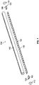
- an LED bulb generally labeled 100, includes a printed circuit board ("PCB") 102 on which there are LED lights 104.
- Each LED light 104 may include an LED and a lens.
- a first pair of pins 106 is attached to a first end of the PCB 102 and a second pair of pins 108 is attached to a second end of the PCB 102.
- the pins 106 form a first bi-pin and the pins 108 form a second bi-pin.
- the first and second bi-pins are configured to fit into a standard tube-style fluorescent light socket.
- the bulb 100 is configured to be a replacement for a fluorescent bulb.
- the PCB 102 is contained in a housing 110, at least a portion of which is translucent or transparent.
- a first end cap 112 closes off the housing 110 at a first end and a second end cap 114 closes off the housing 110 at a second end.
- the first and second end caps each have a pair of holes through which the pins (of the first and second bi-pins) pass.
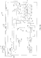
- FIG. 2A a block diagram of a light fixture configured according to an embodiment is shown.
- the light fixture generally labeled 200, includes a ballast 202 that receives power in the form of a 115 volt alternating current ("VAC") with a frequency of 400 Hertz ("Hz"). It is to be understood that the current, voltage, and frequency values disclosed herein are merely illustrative and other values may be used.
- the light fixture 200 further includes an LED replacement bulb 204 ("bulb 204").
- the bulb 204 may have the configuration depicted in FIG. 1 .
- the bulb 204 includes bi-pins 205A, 205B, 205C, and 205D, a bridge rectifier 206 ("rectifier 206") that receives alternating current (“AC") from the ballast 202 (via the bi-pins 205A and 205B) and rectifies the AC into direct current (“DC”). Put another way, the rectifier 206 converts the AC voltage received by the bulb 204 into a DC voltage.
- alternating current AC
- DC direct current
- the bulb 204 further includes a voltage regulator 208 that regulates the voltage of the DC current, a temperature sensor 210 that senses the temperature of the bulb 204 (particularly in the vicinity of the LED lights, such as at the PCB 102), logic circuitry 212, a differential amplifier 214, transistor 216, resistive elements 218 (e.g., ballast resistors), safety circuit 220, and a sense resistor 222.
- a field-effect transistor e.g., a metal oxide semiconductor FET (“MOSFET”).
- MOSFET metal oxide semiconductor FET
- the resistive elements 218 are electrically connected in series along a circuit path 226, which extends from a node 225 having a voltage of Vrect (i.e., the voltage output of the rectifier 206). Also extending from (and electrically connected to) the node 225 are a branch 227 and a branch 229.
- the branch 227 includes LED lights 230A of one color (e.g., white) electrically connected in series as light strings 230 along parallel sub-branches 232, 234, and 236.
- the branch 229 includes LED lights 238A of another color (e.g., blue) electrically connected in series as light strings 238 along parallel sub-branches 240, 242, and 244.
- resistive elements 240A, 242A, and 244A Electrically connected in series with each light string 238 of each sub-branch 240, 242, and 244 are respective resistive elements 240A, 242A, and 244A.
- resistive elements 240A, 242A, and 244A will often be referred to as “resistors,” though other types of resistive elements are possible.
- the present disclosure will sometimes refer to the branch 227 as the "first branch” and the branch 229 as the “second branch.” On other occasions the references are reversed, depending on the order in which they are described. Furthermore, the present disclosure may refer to the color of the LEDs of the branch 227 as the "first color” and refer to the color of the LEDs of the second branch 229 as the “second color.” On other occasions the references are reversed, depending on the order in which they are described.
- Possible implementations of the logic circuitry 212 include a microprocessor, microcontroller, application-specific integrated circuit (“ASIC”), and field-programmable gate array (“FPGA”).
- ASIC application-specific integrated circuit
- FPGA field-programmable gate array
- the fixture 200 would be electrically linked to, for example, a cabin control panel 201.
- a cabin control panel 201 any sort of program that a flight attendant would initiate via the cabin control panel 201 (e.g., a "mealtime" program), which resulted in the cabin control panel dimming or raising the cabin lights would translate into a color change in the bulb 204.
- this color change would occur by virtue of the raising and lowering to current to the bulb 204 without the need for packet-based communiation or other types of "smart" signaling.
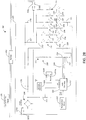
- FIG. 2B another embodiment of the bulb 204 is shown.
- the difference between this embodiment and the embodiment of FIG. 2A is that, in the embodiment of FIG. 2B , there are no series resistors in the branch 229. Instead, there is a transistor 221 that is under the control of the logic circuitry 212.
- the embodiment of FIG. 2B uses the logic circuitry 212 to open and close the gate of the transistor 221, which itself controls the voltage drop across the transistor 221. It is possible that one or more fixed resistors could be placed in the branch 229, but the bulk of the control as to whether current is permitted to or restricted from traveling the branch 229 would be provided by the transistor 221.
- the logic circuitry receives, at an input port 213 (depicted as an analog to digital (“A/D") converter in FIG. 2B ) a signal representing a voltage across a sense resistor 215.
- the logic circuitry 212 analyzes this signal to determine the current being output by the ballast 202.
- the logic circuitry 212 refers to a data structure 212B stored in a memory 212A of the logic circuitry.
- the data structure 212B (e.g., a look up table or call-able function) maps the ballast output (e.g., the ballast current) to one or more LED colors and/or LED brightness.
- the data structure 212B may specify that when the ballast current decreases past a certain threshold, the LEDs of the branch 227 are to be dimmed (thereby increasing the percentage of light from the bulb 204 being supplied by the LEDs of the branch 229).
- a change in current from the ballast 202 results in a color transition.
- the LED lights 230A of the branch 227 are white and the LED lights 238A of the branch 229 are blue.
- the voltage across the resistor for each string (240A, 242A, and 244A) is not enough to make up for the fact that there are more white LED lights than blue LED lights (i.e., the total resistance of the white LEDs exceeds that of the blue LEDs, particularly at low current, and the resistor will not make much of a difference at low current).
- the light output by the bulb 204 will be, for example, 100% blue and 0% warm white.
- the voltage drop across of the resistor starts to equal the voltage drop across the white LED lights (with the blue LED lights contributing relatively little in terms of voltage drop) and the current is split between the two branches, resulting in a light from the bulb 204 that is cool white (50% blue and 50% warm white).
- the blue LED lights will be at their maximum brightness (as limited by the resistor).
- the ballast current increases to its maximum, all of the "extra" current goes to path of least resistance which is the branch 227.
- the resulting output from the bulb 204 will be, for example, neutral white and composed of 20% blue and 80% warm white.
- FIG. 3A an example of how a replacement LED bulb transitions from one color to another as a result of a dimming operation carried out by the fixture 200 (according to an embodiment) will now be described.
- the ballast 202 outputs it maximum current (e.g., 300 mA).
- the logic circuitry 212 may have the gate of the transistor 221 of the transistor 221 open (so as to allow the LED lights of the strings 238 to illuminate) or may have the gate of the transistor 221 of the transistor closed (so as to prevent the LED lights of the strings 238 from illuminating).
- the voltage drop across the transistor 221 is sufficiently high (very high, if the gate of the transistor 221 is closed) so that overall voltage drop on the branch 229 is lower than that on the branch 227, resulting in a current flow to the branch 229.
- the ballast 202 decreases its current output (e.g., to 200 mA) to a point wheren the voltage across the respective LED lights of the branch 227 approach their respective forward voltages and the LED lights 230A dim.
- the logic circuitry 212 detects this decrease (at the input 213 via the parasitic resistor 215) and may (a) respond by opening the gate of the transistor 221 of the second transistor 221 (either from a closed state or from one open state to another) to draw current down the branch 229 and thereby illuminate the LED lights 238A of the branch 229 (if they were not already lit) and/or (b) output a pulse width-modulated (“PWM”) signal to the string 227 in order to keep the LED lights of the string 227 lit for a transition effect.
- PWM pulse width-modulated
- the ballast 202 outputs a current at a third level (e.g., 100 mA) and the LED lights 230A of the string 227 turn off, either as a result of (a) the voltages across the lights of the string 227 dropping below their respective forward voltages or (b) the logic circuitry 212 stops outputting a PWM to the string 227.
- a third level e.g. 100 mA
- the ballast 202 decreases its current output and the lights of the branch 229 dim and ultimately cease to be illuminated due to (a) the overall current available from the node 225 being too low to provide sufficient voltage across the LED lights 238A and/or (b) the logic circuitry 212 closing the gate of the transistor 221 of the transistor 221 to restrict (and shut off) the flow of current through the transistor 221.
- the ballast 202 outputs a current at a fourth level, which is very low or at zero.
- the ballast 202 outputs no current or a minimum amount of current (e.g., enough to power the logic circuitry 212).
- the gate of the transistor 221 of the transistor 221 is closed and no LED lights are illuminated. open (so as to allow the LED lights 238A of the strings 238 to illuminate) or may have the gate of the transistor 221 closed (so as to prevent the LED lights of the strings 238 from illuminating).
- the ballast 202 increases its output to a first current level (e.g., 100 mA).
- the logic circuitry 212 detects this change at block 352 (time T1), and response by applying a voltage to the gate of the transistor 221 of the transistor 221, thereby opening the gate of the transistor 221. This action decreases the voltage drop on the branch 229 to a point where that voltage drop is less than the voltage drop across the branch 227. This has the effect of drawing the current to the branch 229. Once the flow of current down the branch 229 is sufficient to cause the voltage across the respective LED lights 238A of the branch 229, those LED lights 238A begin to illuminate. From time T1 to time T2, the current output by the ballast 202 continues to increase and the lights of the branch 229 become brighter.
- the current in the branch 229 is high enough (e.g., 200 mA) that the voltage drop across the transistor 221 is significant enough to cause the voltage drop across the branch 229 to exceed that of the branch 227, thereby causing the current on the node 225 to start diverting to the branch 227.
- the current output by the ballast 202 continues to increase, as does the amount of current going to the branch 227.
- the voltage across the respective LED lights 230A of the branch 227 exceed their respective forward voltages and, as a result, the LED lights 230A of the branch 227 begin to illuminate.
- the ballast 202 increases its current output until it's maximum (e.g., 300 mA) (at block 356, time T4), during which time the LED lights 230A of the branch 227 continue to brighten.
- the logic circuitry 212 may (a) allow the LED lights 230A of the branch 227 to remain on or (b) close the gate of the transistor 221 of the transistor 221 to restrict the flow of current down the branch 229 to cause the LED lights 238A of the branch 229 to stop emitting light.
- the logic circuitry 212 may carry out a transition effect (e.g., a fade over effect) from the LED lights 238A of the branch 229 to the LED lights 230A of the branch 227 by outputting a PWM signal to the LED lights 238A of the branch 229 (even if the LED lights 238A are not receiving sufficient current from the node 225).
- a transition effect e.g., a fade over effect
- FIGS. 3A and 3B may be overlapping in time, though they are depicted as occurring in a non-overlapping manner.
- a line graph illustrates the relationship (according to an embodiment) between the ballast current, the output of the LEDs 238A (assumed to be blue in this example) (line 402 of the graph), the output of the LEDs 230A (assumed to be white in this example) (line 404 of the graph), and the overall color temperature of the light output by the bulb 204 (line 406 of the graph). Note that because the blue LED lights are in series with resistors, their output increases more slowly (as a function of the ballast curret) than the output of the white LEDs. Once the white LEDs are able to turn on, they quickly take over for the majority of the overall light output.
- the light fixture 200 when the light fixture 200 is initially turned on, only the blue LED is on. Then there is an intermediate region where the blue LEDs and the white LEDs are on. As the power to the bulb 204 increases (e.g., due to the dimmer switch being increased), the bulb enters a bright region where the majority of the light output is due to the white LEDs. Overall, from start to finish, the color temperature goes from basic blue (about 4000K) to 10000K (which is a mix of white and blue).
- an embodiment of the LED replacement bulb may be programmed to react in different ways to different ballast currents.
- one mechanism for carrying out such programming is an appliance configured to electrically connect to the bulb.
- FIG. 5 depicts how such an appliance may be implemented.
- the appliance 500 has an open-faced chamber 502 that is sized to fit a bulb. Within the chamber 502 are sockets 504A and 504B, which are configured to receive bi-pins of the bulb (such as the bi-pins shown in FIG. 1 , FIG. 2A , and FIG. 2B ).
- the appliance 500 includes controls for power (power switch 508), selecting "bright” or “dim” (select button 510) and locking in a selection (the set button 512).
- Indicator lights 514 show which selection has been made between “bright” and “dim”
- indicator lights 516 show which selection has been made as between a first color (color A) and a second color (color B).
- the appliance 400 transmits those selections to the logic circuitry 212 (via one or more of the bi-pins 205A, 205B, 205C, and 205D).
- the logic circuitry 212 stores those selections in the data structure 212B.
Landscapes
- Engineering & Computer Science (AREA)
- Physics & Mathematics (AREA)
- Microelectronics & Electronic Packaging (AREA)
- Optics & Photonics (AREA)
- General Engineering & Computer Science (AREA)
- Circuit Arrangement For Electric Light Sources In General (AREA)
Abstract
Description
- The present disclosure relates generally to light-emitting diode ("LED") lighting and, more particularly, to an LED bulb for use as a replacement for a fluorescent bulb.
- Fluorescent lighting is a relatively old technology. With LED lights becoming more popular, a market for LED replacement bulbs that fit into fluorescent light fixtures has developed. Although LED replacement bulbs give off a higher quality light that lacks the flickering that is characteristic of fluorescent bulbs, they are still generally confined to a single color per bulb. Typically, it takes an extensive retrofit of lighting system in order to take full advantage of the potential lighting effects that can be attained with LEDs.
- While the appended claims set forth the features of the present techniques with particularity, these techniques, together with their objects and advantages, may be best understood from the following detailed description taken in conjunction with the accompanying drawings of which:
-
FIG. 1 is a disassembled view of an LED bulb configured according to an embodiment. -
FIG. 2A andFIG. 2B are block diagrams of a light fixture configured according to different embodiments. -
FIGS. 3A and3B are diagrams showing the actions carried out during dimming or brightening, according to an embodiment. -
FIG. 4 is a line graph showing the relative change in blue light LED output, white light LED output, and color temperature of an LED bulb at different percentages of ballast current and different percentages of overall light output, according to an embodiment. -
FIG. 5 is an elevated view of an appliance used for programming an LED bulb, according to an embodiment. - Various embodiments of the present disclosure include an LED replacement bulb having the same physical shape and appearance as a fluorescent bulb, but having the superior illumination characteristics of LED lights (e.g., the ability to dim, the absence of flicker) and the ability to switch (with or without transition) from a first color to a second color while the LED lighting assembly undergoes a dimming or brightening procedure. Furthermore, because the bulb uses the output of the light fixture (e.g., the output of the ballast of a fluorescent light fixture) as the cue for whether to change colors, no retrofitting of the lighting system is required (as might be the case if more modem, network-addressable light units were required).
- Turning to
FIG. 1 , an LED bulb, generally labeled 100, includes a printed circuit board ("PCB") 102 on which there areLED lights 104. EachLED light 104 may include an LED and a lens. A first pair ofpins 106 is attached to a first end of thePCB 102 and a second pair ofpins 108 is attached to a second end of thePCB 102. In effect, thepins 106 form a first bi-pin and thepins 108 form a second bi-pin. The first and second bi-pins are configured to fit into a standard tube-style fluorescent light socket. Overall, thebulb 100 is configured to be a replacement for a fluorescent bulb. - The PCB 102 is contained in a
housing 110, at least a portion of which is translucent or transparent. Afirst end cap 112 closes off thehousing 110 at a first end and asecond end cap 114 closes off thehousing 110 at a second end. The first and second end caps each have a pair of holes through which the pins (of the first and second bi-pins) pass. - Turning to
FIG. 2A , a block diagram of a light fixture configured according to an embodiment is shown. The light fixture, generally labeled 200, includes aballast 202 that receives power in the form of a 115 volt alternating current ("VAC") with a frequency of 400 Hertz ("Hz"). It is to be understood that the current, voltage, and frequency values disclosed herein are merely illustrative and other values may be used. Thelight fixture 200 further includes an LED replacement bulb 204 ("bulb 204"). Thebulb 204 may have the configuration depicted inFIG. 1 . Thebulb 204 includesbi-pins rectifier 206") that receives alternating current ("AC") from the ballast 202 (via thebi-pins rectifier 206 converts the AC voltage received by thebulb 204 into a DC voltage. Thebulb 204 further includes avoltage regulator 208 that regulates the voltage of the DC current, atemperature sensor 210 that senses the temperature of the bulb 204 (particularly in the vicinity of the LED lights, such as at the PCB 102),logic circuitry 212, adifferential amplifier 214,transistor 216, resistive elements 218 (e.g., ballast resistors),safety circuit 220, and asense resistor 222. Possible implementations of thetransistor 216 include a field-effect transistor (e.g., a metal oxide semiconductor FET ("MOSFET")). Thetemperature sensor 210 and thelogic circuitry 212 both receive power from thevoltage regulator 208. Theresistive elements 218 are electrically connected in series along acircuit path 226, which extends from anode 225 having a voltage of Vrect (i.e., the voltage output of the rectifier 206). Also extending from (and electrically connected to) thenode 225 are abranch 227 and abranch 229. Thebranch 227 includesLED lights 230A of one color (e.g., white) electrically connected in series aslight strings 230 alongparallel sub-branches branch 229 includesLED lights 238A of another color (e.g., blue) electrically connected in series aslight strings 238 alongparallel sub-branches light string 238 of eachsub-branch resistive elements resistive elements - The present disclosure will sometimes refer to the
branch 227 as the "first branch" and thebranch 229 as the "second branch." On other occasions the references are reversed, depending on the order in which they are described. Furthermore, the present disclosure may refer to the color of the LEDs of thebranch 227 as the "first color" and refer to the color of the LEDs of thesecond branch 229 as the "second color." On other occasions the references are reversed, depending on the order in which they are described. - Possible implementations of the
logic circuitry 212 include a microprocessor, microcontroller, application-specific integrated circuit ("ASIC"), and field-programmable gate array ("FPGA"). - Although not required for this disclosure, one possible deployment scenario for the
bulb 204 is within a light fixture of an aircraft cabin. In such a scenario, thefixture 200 would be electrically linked to, for example, acabin control panel 201. Thus, any sort of program that a flight attendant would initiate via the cabin control panel 201 (e.g., a "mealtime" program), which resulted in the cabin control panel dimming or raising the cabin lights would translate into a color change in thebulb 204. As will be described in further detail, this color change would occur by virtue of the raising and lowering to current to thebulb 204 without the need for packet-based communiation or other types of "smart" signaling. - Turning to
FIG. 2B , another embodiment of thebulb 204 is shown. The difference between this embodiment and the embodiment ofFIG. 2A is that, in the embodiment ofFIG. 2B , there are no series resistors in thebranch 229. Instead, there is atransistor 221 that is under the control of thelogic circuitry 212. Thus, instead of relying on a resistor-induced voltage drop (as in the embodiment ofFIG. 2A ), the embodiment ofFIG. 2B uses thelogic circuitry 212 to open and close the gate of thetransistor 221, which itself controls the voltage drop across thetransistor 221. It is possible that one or more fixed resistors could be placed in thebranch 229, but the bulk of the control as to whether current is permitted to or restricted from traveling thebranch 229 would be provided by thetransistor 221. - To determine whether and how to control
transistor 221, the logic circuitry receives, at an input port 213 (depicted as an analog to digital ("A/D") converter inFIG. 2B ) a signal representing a voltage across asense resistor 215. Thelogic circuitry 212 analyzes this signal to determine the current being output by theballast 202. Using this information, thelogic circuitry 212 refers to adata structure 212B stored in amemory 212A of the logic circuitry. Thedata structure 212B (e.g., a look up table or call-able function) maps the ballast output (e.g., the ballast current) to one or more LED colors and/or LED brightness. For example, thedata structure 212B may specify that when the ballast current decreases past a certain threshold, the LEDs of thebranch 227 are to be dimmed (thereby increasing the percentage of light from thebulb 204 being supplied by the LEDs of the branch 229). - Operation of the embodiment of the
bulb 204 shown inFIG. 2A according to an embodiment will now be described. A change in current from theballast 202 results in a color transition. To illustrate with a concrete example, assume that theLED lights 230A of thebranch 227 are white and theLED lights 238A of thebranch 229 are blue. When the current from theballast 202 is low, the voltage across the resistor for each string (240A, 242A, and 244A) is not enough to make up for the fact that there are more white LED lights than blue LED lights (i.e., the total resistance of the white LEDs exceeds that of the blue LEDs, particularly at low current, and the resistor will not make much of a difference at low current). As a result, the light output by thebulb 204 will be, for example, 100% blue and 0% warm white. When the current from theballast 202 is at a medium level, the voltage drop across of the resistor starts to equal the voltage drop across the white LED lights (with the blue LED lights contributing relatively little in terms of voltage drop) and the current is split between the two branches, resulting in a light from thebulb 204 that is cool white (50% blue and 50% warm white). At some point, the blue LED lights will be at their maximum brightness (as limited by the resistor). As the ballast current increases to its maximum, all of the "extra" current goes to path of least resistance which is thebranch 227. The resulting output from thebulb 204 will be, for example, neutral white and composed of 20% blue and 80% warm white. - It is to be understood that the ratios and values in the foregoing example are meant only to be illustrative and that the numbers are meant to be general ratios. Furthermore, there can be other colors and combinations, such as warm and cool white or blue and red.
- Turning to
FIG. 3A , an example of how a replacement LED bulb transitions from one color to another as a result of a dimming operation carried out by the fixture 200 (according to an embodiment) will now be described. At time T0 (block 302), it will be assumed that theballast 202 outputs it maximum current (e.g., 300 mA). At this point, thelogic circuitry 212 may have the gate of thetransistor 221 of thetransistor 221 open (so as to allow the LED lights of thestrings 238 to illuminate) or may have the gate of thetransistor 221 of the transistor closed (so as to prevent the LED lights of thestrings 238 from illuminating). In either case, the voltage drop across thetransistor 221 is sufficiently high (very high, if the gate of thetransistor 221 is closed) so that overall voltage drop on thebranch 229 is lower than that on thebranch 227, resulting in a current flow to thebranch 229. Theballast 202 decreases its current output (e.g., to 200 mA) to a point wheren the voltage across the respective LED lights of thebranch 227 approach their respective forward voltages and theLED lights 230A dim. Atblock 304, thelogic circuitry 212 detects this decrease (at theinput 213 via the parasitic resistor 215) and may (a) respond by opening the gate of thetransistor 221 of the second transistor 221 (either from a closed state or from one open state to another) to draw current down thebranch 229 and thereby illuminate theLED lights 238A of the branch 229 (if they were not already lit) and/or (b) output a pulse width-modulated ("PWM") signal to thestring 227 in order to keep the LED lights of thestring 227 lit for a transition effect. Atblock 306, theballast 202 outputs a current at a third level (e.g., 100 mA) and theLED lights 230A of thestring 227 turn off, either as a result of (a) the voltages across the lights of thestring 227 dropping below their respective forward voltages or (b) thelogic circuitry 212 stops outputting a PWM to thestring 227. - As the time moves from T2 to T3, the
ballast 202 decreases its current output and the lights of thebranch 229 dim and ultimately cease to be illuminated due to (a) the overall current available from thenode 225 being too low to provide sufficient voltage across theLED lights 238A and/or (b) thelogic circuitry 212 closing the gate of thetransistor 221 of thetransistor 221 to restrict (and shut off) the flow of current through thetransistor 221. At block 308 (time T3), theballast 202 outputs a current at a fourth level, which is very low or at zero. - Turning to
FIG. 3B , an example of how thebulb 100 transitions from one color to another as a result of a dimming operation carried out by thefixture 200 will now be described. At time T0 (block 350), it will be assumed that theballast 202 outputs no current or a minimum amount of current (e.g., enough to power the logic circuitry 212). At this point, the gate of thetransistor 221 of thetransistor 221 is closed and no LED lights are illuminated. open (so as to allow theLED lights 238A of thestrings 238 to illuminate) or may have the gate of thetransistor 221 closed (so as to prevent the LED lights of thestrings 238 from illuminating). Theballast 202 increases its output to a first current level (e.g., 100 mA). Thelogic circuitry 212 detects this change at block 352 (time T1), and response by applying a voltage to the gate of thetransistor 221 of thetransistor 221, thereby opening the gate of thetransistor 221. This action decreases the voltage drop on thebranch 229 to a point where that voltage drop is less than the voltage drop across thebranch 227. This has the effect of drawing the current to thebranch 229. Once the flow of current down thebranch 229 is sufficient to cause the voltage across therespective LED lights 238A of thebranch 229, those LEDlights 238A begin to illuminate. From time T1 to time T2, the current output by theballast 202 continues to increase and the lights of thebranch 229 become brighter. At block 352 (time T2), the current in thebranch 229 is high enough (e.g., 200 mA) that the voltage drop across thetransistor 221 is significant enough to cause the voltage drop across thebranch 229 to exceed that of thebranch 227, thereby causing the current on thenode 225 to start diverting to thebranch 227. From time T2 to time T3, the current output by theballast 202 continues to increase, as does the amount of current going to thebranch 227. At block 354 (time T3), the voltage across therespective LED lights 230A of thebranch 227 exceed their respective forward voltages and, as a result, theLED lights 230A of thebranch 227 begin to illuminate. Between time T3 and time T4, theballast 202 increases its current output until it's maximum (e.g., 300 mA) (atblock 356, time T4), during which time theLED lights 230A of thebranch 227 continue to brighten. Thelogic circuitry 212 may (a) allow theLED lights 230A of thebranch 227 to remain on or (b) close the gate of thetransistor 221 of thetransistor 221 to restrict the flow of current down thebranch 229 to cause theLED lights 238A of thebranch 229 to stop emitting light. Additionally, thelogic circuitry 212 may carry out a transition effect (e.g., a fade over effect) from theLED lights 238A of thebranch 229 to theLED lights 230A of thebranch 227 by outputting a PWM signal to theLED lights 238A of the branch 229 (even if the LED lights 238A are not receiving sufficient current from the node 225). - It should be noted that the actions described in conjunction with
FIGS. 3A and3B may be overlapping in time, though they are depicted as occurring in a non-overlapping manner. - Turning to
FIG. 4 , a line graph illustrates the relationship (according to an embodiment) between the ballast current, the output of theLEDs 238A (assumed to be blue in this example) (line 402 of the graph), the output of theLEDs 230A (assumed to be white in this example) (line 404 of the graph), and the overall color temperature of the light output by the bulb 204 (line 406 of the graph). Note that because the blue LED lights are in series with resistors, their output increases more slowly (as a function of the ballast curret) than the output of the white LEDs. Once the white LEDs are able to turn on, they quickly take over for the majority of the overall light output. Thus, when thelight fixture 200 is initially turned on, only the blue LED is on. Then there is an intermediate region where the blue LEDs and the white LEDs are on. As the power to thebulb 204 increases (e.g., due to the dimmer switch being increased), the bulb enters a bright region where the majority of the light output is due to the white LEDs. Overall, from start to finish, the color temperature goes from basic blue (about 4000K) to 10000K (which is a mix of white and blue). - As noted in the description of
FIG. 2B , an embodiment of the LED replacement bulb may be programmed to react in different ways to different ballast currents. According to an embodiment, one mechanism for carrying out such programming is an appliance configured to electrically connect to the bulb.FIG. 5 depicts how such an appliance may be implemented. Theappliance 500 has an open-facedchamber 502 that is sized to fit a bulb. Within thechamber 502 aresockets FIG. 1 ,FIG. 2A , andFIG. 2B ). Theappliance 500 includes controls for power (power switch 508), selecting "bright" or "dim" (select button 510) and locking in a selection (the set button 512).Indicator lights 514 show which selection has been made between "bright" and "dim," andindicator lights 516 show which selection has been made as between a first color (color A) and a second color (color B). Once the user (e.g., a customer of the bulb manufacturer) has made and locked in the desired selections (e.g., a bright setting = color A, and a dim setting = color B or vice versa), the appliance 400 transmits those selections to the logic circuitry 212 (via one or more of the bi-pins 205A, 205B, 205C, and 205D). Thelogic circuitry 212 stores those selections in thedata structure 212B. - It should be understood that the embodiments described herein should be considered in a descriptive sense only and not for purposes of limitation. Descriptions of features or aspects within each embodiment should typically be considered as available for other similar features or aspects in other embodiments. It will be understood by those of ordinary skill in the art that various changes in form and details may be made therein without departing from their spirit and scope.
Claims (14)
- A light emitting diode (LED) bulb comprising:an electrical circuit comprising:a node that carries a current;a first branch that extends from the node to ground, wherein the first branch includes a plurality of LEDs of a first color;a second branch that extends from the node to ground, wherein the second branch includes a plurality of LEDs of a second color and a resistive element in series with the plurality of LEDs of the second color, wherein the value of the resistive element is such that:when the current is at a first level, the voltage drop on the second branch is less than the voltage drop on the first branch, thereby drawing the current down the second branch so as to illuminate the plurality of LEDs of the second color;when the current is at a second level, the voltage drop on the second branch is approximate equal to the voltage drop on the first branch, thereby drawing the current down both the first and the second branch so as to illuminate the plurality of LEDs of the second color and to begin to illuminate the plurality of LEDs of the first color,wherein the second level is higher than the first level; andas the current rises beyond the second level, the voltage drop on the first branch is lower than the voltage drop on the second branch, thereby drawing more current down the first branch and illuminating the LED lights of the first color more than the LED lights of the second color.
- The bulb of claim 1, wherein the number of LED lights in the first branch exceeds the number of LED lights in the second branch.
- The bulb of claim 1 or 2, wherein the first branch includes a plurality of sub-branches, each sub-branch including a string of LED lights of the first color.
- The bulb of claim 1 or 2, wherein the second branch includes a plurality of sub-branches, each sub-branch including a string of LED lights of the second color and a resistive element in parallel with the string of LED lights.
- The bulb of claim 1 or 2, wherein:the first branch includes a plurality of sub-branches, each sub-branch including a string of LED lights of the first color, andwherein the second branch includes a plurality of sub-branches, each sub-branch including a string of LED lights of the second color and a resistive element in parallel with the string of LED lights.
- The bulb of claim 5, wherein the number of LED lights in each of the sub-branches of the first branch exceeds the number of LED lights in each of the sub-branches of the second branch.
- A method for changing colors in a light emitting diode (LED) bulb, wherein the bulb comprises a first string of LED lights of a first color and a second string of LED lights of a second color, method comprising:detecting the level of current being provided to the bulb by a light fixture;when the detected level is a first level, opening a gate of a transistor connected in series with the first string of LED lights to permit a current that is internal to the LED replacement bulb to flow through the first string of LED lights in order to illuminate the LED lights of the first string; andwhen the detected level is a second level, begin closing the gate of the first transistor in order to reduce the brightness of the LED lights of the first string,wherein the second level is higher than the first level.
- The method of claim 7, further comprising:when the detected level is a third level, closing the gate of the first resistor in order to turn off the LED lights of the first string, wherein the third level is higher than the second level.
- The method of claim 7 or 8, wherein there are no resistors in series with either the first or the second strings.
- The method of any of claims 7 through 9, wherein the first branch includes a plurality of sub-branches, each sub-branch including a string of LED lights of the first color.
- The method of any of claims 7 through 9, wherein the second branch includes a plurality of sub-branches, each sub-branch including a string of LED lights of the second color.
- The method of any of claims 7 through 9, wherein:the first branch includes a plurality of sub-branches, each sub-branch including a string of LED lights of the first color, andwherein the second branch includes a plurality of sub-branches, each sub-branch including a string of LED lights of the second color.
- A light emitting diode (LED) bulb comprising:a first string of LED lights of a first color;a transistor electrically connected in series with the LED lights of the first string;a second string of LED lights of a second color;logic circuitry configured to:detect a current being output to the bulb by a ballast;when the detected current has dropped to a first level, close a gate of the first transistor to restrict the amount of current flowing to the first string of LEDs in order to reduce the amount of light output by the LED lights of the first string; andwhen the detected level is a second level, begin closing the gate of the first transistor in order to reduce the brightness of the LED lights of the first string,wherein the second level is lower than the first level.
- The bulb of claim 13, wherein the logic circuitry is further configured to:after the detected level has dropped to the first level, transmit a pulse-wave modulated signal to the first string in order create transition effect from the first color to the second color.
Applications Claiming Priority (1)
| Application Number | Priority Date | Filing Date | Title |
|---|---|---|---|
| US15/451,651 US10104730B2 (en) | 2017-03-07 | 2017-03-07 | LED bulb and method for operating same |
Publications (2)
| Publication Number | Publication Date |
|---|---|
| EP3373703A1 true EP3373703A1 (en) | 2018-09-12 |
| EP3373703B1 EP3373703B1 (en) | 2022-12-28 |
Family
ID=61256664
Family Applications (1)
| Application Number | Title | Priority Date | Filing Date |
|---|---|---|---|
| EP18157824.6A Active EP3373703B1 (en) | 2017-03-07 | 2018-02-21 | Led bulb and method for operating same |
Country Status (4)
| Country | Link |
|---|---|
| US (1) | US10104730B2 (en) |
| EP (1) | EP3373703B1 (en) |
| CN (1) | CN108571665B (en) |
| CA (1) | CA2994426A1 (en) |
Families Citing this family (1)
| Publication number | Priority date | Publication date | Assignee | Title |
|---|---|---|---|---|
| US11490484B1 (en) | 2021-10-15 | 2022-11-01 | Aircraft Lighting International Inc. | Retrofit light-emitting diode lamp and circuit thereof |
Citations (11)
| Publication number | Priority date | Publication date | Assignee | Title |
|---|---|---|---|---|
| WO2008041153A1 (en) * | 2006-10-06 | 2008-04-10 | Philips Intellectual Property & Standards Gmbh | Power supply device for light elements and method for supplying power to light elements |
| WO2010122463A1 (en) * | 2009-04-23 | 2010-10-28 | Koninklijke Philips Electronics N.V. | Driver for an led lamp |
| WO2012044223A1 (en) * | 2010-07-29 | 2012-04-05 | Andreas Vinnberg | Led lamp |
| DE102011087658A1 (en) * | 2011-12-02 | 2013-06-06 | Osram Gmbh | Parallel connected light chains |
| WO2013173284A1 (en) * | 2012-05-14 | 2013-11-21 | Usai, Llc | Lighting system having a dimming color simulating an incandescent light |
| WO2013171622A1 (en) * | 2012-05-15 | 2013-11-21 | Koninklijke Philips N.V. | Light source circuitry |
| EP2760254A1 (en) * | 2013-01-25 | 2014-07-30 | Dialog Semiconductor Inc. | Adjusting color temperature in a dimmable LED lighting system |
| DE102013207245A1 (en) * | 2013-04-22 | 2014-10-23 | Osram Gmbh | Control of semiconductor light elements |
| US8907576B2 (en) * | 2013-01-28 | 2014-12-09 | Lumenetix, Inc. | Linear bypass electrical circuit for driving LED strings |
| US20150137689A1 (en) * | 2013-11-18 | 2015-05-21 | Cree, Inc. | Systems and methods for a current sharing driver for light emitting diodes |
| US9049769B2 (en) * | 2012-06-07 | 2015-06-02 | Seckin KEMAL SECILMIS | LED light bulb with failure indication and color change capability |
Family Cites Families (18)
| Publication number | Priority date | Publication date | Assignee | Title |
|---|---|---|---|---|
| US6184628B1 (en) * | 1999-11-30 | 2001-02-06 | Douglas Ruthenberg | Multicolor led lamp bulb for underwater pool lights |
| US7375476B2 (en) * | 2005-04-08 | 2008-05-20 | S.C. Johnson & Son, Inc. | Lighting device having a circuit including a plurality of light emitting diodes, and methods of controlling and calibrating lighting devices |
| EP1787886B1 (en) * | 2005-11-18 | 2008-01-02 | ALCATEL Transport Solution Deutschland GmbH | Electrical circuit for an LED signal lamp with a switching threshold for switching between a daylight operation mode and a nighttime operation mode |
| CA2720313C (en) * | 2008-04-04 | 2016-11-08 | Ideal Industries Lighting Llc | Led light fixture |
| US8569956B2 (en) * | 2009-06-04 | 2013-10-29 | Point Somee Limited Liability Company | Apparatus, method and system for providing AC line power to lighting devices |
| US8710754B2 (en) * | 2011-09-12 | 2014-04-29 | Juno Manufacturing Llc | Dimmable LED light fixture having adjustable color temperature |
| US9468062B2 (en) * | 2013-01-02 | 2016-10-11 | Austin Ip Partners | Light emitting diode light structures |
| US9899914B2 (en) * | 2014-09-30 | 2018-02-20 | Panasonic Intellectual Property Management Co., Ltd. | Light switch device |
| US9970639B2 (en) * | 2014-12-18 | 2018-05-15 | Hubbell Incorporated | Circuit boards for LED-based light fixtures |
| US9468060B2 (en) * | 2015-03-04 | 2016-10-11 | Lunera Lighting, Inc. | ANSI reference ballast compliance circuit for LED retrofit lamps |
| WO2017012835A1 (en) * | 2015-07-21 | 2017-01-26 | Philips Lighting Holding B.V. | Tapped linear driver and driving method |
| CN204993998U (en) * | 2015-09-15 | 2016-01-20 | 厦门高贤电子科技有限公司 | Curved circuit structure of adjustable LED colour temperature |
| TWM524800U (en) * | 2016-03-11 | 2016-07-01 | 威力暘電子股份有限公司 | Multi-lamp group failure control circuit device |
| CN105704865A (en) * | 2016-04-24 | 2016-06-22 | 吴圣铎 | Safety commanding LED indicator lamp used for vehicle access in underground parking |
| CN205946237U (en) * | 2016-06-01 | 2017-02-08 | 四川欧利普照明科技开发有限公司 | High -power LED lamp drive power supply |
| CN106061015A (en) * | 2016-06-18 | 2016-10-26 | 吴圣铎 | Touch delay gradually-brightening and gradually-dimming LED (Light-Emitting Diode) illuminating lamp |
| CN106028543A (en) * | 2016-07-05 | 2016-10-12 | 成都中冶节能环保工程有限公司 | Overvoltage protective LED energy-saving driving system based on power amplification circuit |
| CN205812466U (en) * | 2016-07-21 | 2016-12-14 | 宁波奇驰照明灯具有限公司 | LED drives control circuit |
-
2017
- 2017-03-07 US US15/451,651 patent/US10104730B2/en active Active
-
2018
- 2018-02-08 CA CA2994426A patent/CA2994426A1/en not_active Abandoned
- 2018-02-21 EP EP18157824.6A patent/EP3373703B1/en active Active
- 2018-03-07 CN CN201810184281.9A patent/CN108571665B/en not_active Expired - Fee Related
Patent Citations (11)
| Publication number | Priority date | Publication date | Assignee | Title |
|---|---|---|---|---|
| WO2008041153A1 (en) * | 2006-10-06 | 2008-04-10 | Philips Intellectual Property & Standards Gmbh | Power supply device for light elements and method for supplying power to light elements |
| WO2010122463A1 (en) * | 2009-04-23 | 2010-10-28 | Koninklijke Philips Electronics N.V. | Driver for an led lamp |
| WO2012044223A1 (en) * | 2010-07-29 | 2012-04-05 | Andreas Vinnberg | Led lamp |
| DE102011087658A1 (en) * | 2011-12-02 | 2013-06-06 | Osram Gmbh | Parallel connected light chains |
| WO2013173284A1 (en) * | 2012-05-14 | 2013-11-21 | Usai, Llc | Lighting system having a dimming color simulating an incandescent light |
| WO2013171622A1 (en) * | 2012-05-15 | 2013-11-21 | Koninklijke Philips N.V. | Light source circuitry |
| US9049769B2 (en) * | 2012-06-07 | 2015-06-02 | Seckin KEMAL SECILMIS | LED light bulb with failure indication and color change capability |
| EP2760254A1 (en) * | 2013-01-25 | 2014-07-30 | Dialog Semiconductor Inc. | Adjusting color temperature in a dimmable LED lighting system |
| US8907576B2 (en) * | 2013-01-28 | 2014-12-09 | Lumenetix, Inc. | Linear bypass electrical circuit for driving LED strings |
| DE102013207245A1 (en) * | 2013-04-22 | 2014-10-23 | Osram Gmbh | Control of semiconductor light elements |
| US20150137689A1 (en) * | 2013-11-18 | 2015-05-21 | Cree, Inc. | Systems and methods for a current sharing driver for light emitting diodes |
Also Published As
| Publication number | Publication date |
|---|---|
| CA2994426A1 (en) | 2018-09-07 |
| US10104730B2 (en) | 2018-10-16 |
| CN108571665A (en) | 2018-09-25 |
| EP3373703B1 (en) | 2022-12-28 |
| US20180263086A1 (en) | 2018-09-13 |
| CN108571665B (en) | 2020-06-30 |
Similar Documents
| Publication | Publication Date | Title |
|---|---|---|
| US10187950B2 (en) | Adjusting color temperature in a dimmable LED lighting system | |
| ES2651887T5 (en) | Lighting apparatus and method | |
| US8174212B2 (en) | LED string driver with light intensity responsive to input voltage | |
| CN101653042B (en) | Hue variation of dimmable devices with stable color temperature light sources | |
| JP4081665B2 (en) | LED lighting device and lighting fixture | |
| JP6087828B2 (en) | LED string driving method and driving device | |
| US9544969B2 (en) | Dimmable LED light fixture having adjustable color temperature | |
| US20130300302A1 (en) | Controller Circuit For Half Wave LED Light Strings | |
| CN103327682A (en) | Adaptive filter for LED dimmer | |
| JP2013545238A5 (en) | ||
| US9516717B2 (en) | Dimmable LED illuminating system, driver of the illuminating system, and method of driving the illuminating system | |
| US11963275B2 (en) | Lighting apparatus | |
| EP3373703B1 (en) | Led bulb and method for operating same | |
| JP6682134B2 (en) | LED lighting device | |
| TWI446837B (en) | Operation apparatus and method for combined operation of gas-discharge lamps and semiconductor light sources | |
| CN112040605A (en) | LED lighting device with high voltage linear drive and memory dimming | |
| CN119117043B (en) | Railway LED signal light system and railway LED signal machine | |
| US9155152B2 (en) | Intensity control of LEDs interfacing three-way sockets | |
| JP6391877B1 (en) | LED toning lighting device | |
| TWI625987B (en) | An apparatus for driving leds using high voltage | |
| JP2026057394A (en) | LED light bulb and its control method | |
| TW201325312A (en) | Light emitting apparatus and dimming method | |
| TWI484864B (en) | Led lighting systems, led controllers and led control methods for a string of leds | |
| US20100052535A1 (en) | Miniature light bulb for random high-low twinkle in a series-wired light string |
Legal Events
| Date | Code | Title | Description |
|---|---|---|---|
| PUAI | Public reference made under article 153(3) epc to a published international application that has entered the european phase |
Free format text: ORIGINAL CODE: 0009012 |
|
| STAA | Information on the status of an ep patent application or granted ep patent |
Free format text: STATUS: THE APPLICATION HAS BEEN PUBLISHED |
|
| AK | Designated contracting states |
Kind code of ref document: A1 Designated state(s): AL AT BE BG CH CY CZ DE DK EE ES FI FR GB GR HR HU IE IS IT LI LT LU LV MC MK MT NL NO PL PT RO RS SE SI SK SM TR |
|
| AX | Request for extension of the european patent |
Extension state: BA ME |
|
| STAA | Information on the status of an ep patent application or granted ep patent |
Free format text: STATUS: REQUEST FOR EXAMINATION WAS MADE |
|
| 17P | Request for examination filed |
Effective date: 20190312 |
|
| RBV | Designated contracting states (corrected) |
Designated state(s): AL AT BE BG CH CY CZ DE DK EE ES FI FR GB GR HR HU IE IS IT LI LT LU LV MC MK MT NL NO PL PT RO RS SE SI SK SM TR |
|
| STAA | Information on the status of an ep patent application or granted ep patent |
Free format text: STATUS: EXAMINATION IS IN PROGRESS |
|
| 17Q | First examination report despatched |
Effective date: 20200527 |
|
| REG | Reference to a national code |
Ref country code: DE Ref legal event code: R079 Ref document number: 602018044634 Country of ref document: DE Free format text: PREVIOUS MAIN CLASS: H05B0033080000 Ipc: H05B0045200000 |
|
| RIC1 | Information provided on ipc code assigned before grant |
Ipc: H05B 45/46 20200101ALI20220613BHEP Ipc: F21Y 115/10 20160101ALI20220613BHEP Ipc: F21Y 103/10 20160101ALI20220613BHEP Ipc: F21K 9/27 20160101ALI20220613BHEP Ipc: H05B 45/20 20200101AFI20220613BHEP |
|
| GRAP | Despatch of communication of intention to grant a patent |
Free format text: ORIGINAL CODE: EPIDOSNIGR1 |
|
| STAA | Information on the status of an ep patent application or granted ep patent |
Free format text: STATUS: GRANT OF PATENT IS INTENDED |
|
| INTG | Intention to grant announced |
Effective date: 20220816 |
|
| GRAS | Grant fee paid |
Free format text: ORIGINAL CODE: EPIDOSNIGR3 |
|
| GRAA | (expected) grant |
Free format text: ORIGINAL CODE: 0009210 |
|
| STAA | Information on the status of an ep patent application or granted ep patent |
Free format text: STATUS: THE PATENT HAS BEEN GRANTED |
|
| AK | Designated contracting states |
Kind code of ref document: B1 Designated state(s): AL AT BE BG CH CY CZ DE DK EE ES FI FR GB GR HR HU IE IS IT LI LT LU LV MC MK MT NL NO PL PT RO RS SE SI SK SM TR |
|
| REG | Reference to a national code |
Ref country code: GB Ref legal event code: FG4D |
|
| REG | Reference to a national code |
Ref country code: CH Ref legal event code: EP |
|
| REG | Reference to a national code |
Ref country code: DE Ref legal event code: R096 Ref document number: 602018044634 Country of ref document: DE |
|
| REG | Reference to a national code |
Ref country code: AT Ref legal event code: REF Ref document number: 1541282 Country of ref document: AT Kind code of ref document: T Effective date: 20230115 |
|
| REG | Reference to a national code |
Ref country code: IE Ref legal event code: FG4D |
|
| REG | Reference to a national code |
Ref country code: LT Ref legal event code: MG9D |
|
| PG25 | Lapsed in a contracting state [announced via postgrant information from national office to epo] |
Ref country code: SE Free format text: LAPSE BECAUSE OF FAILURE TO SUBMIT A TRANSLATION OF THE DESCRIPTION OR TO PAY THE FEE WITHIN THE PRESCRIBED TIME-LIMIT Effective date: 20221228 Ref country code: NO Free format text: LAPSE BECAUSE OF FAILURE TO SUBMIT A TRANSLATION OF THE DESCRIPTION OR TO PAY THE FEE WITHIN THE PRESCRIBED TIME-LIMIT Effective date: 20230328 Ref country code: LT Free format text: LAPSE BECAUSE OF FAILURE TO SUBMIT A TRANSLATION OF THE DESCRIPTION OR TO PAY THE FEE WITHIN THE PRESCRIBED TIME-LIMIT Effective date: 20221228 Ref country code: FI Free format text: LAPSE BECAUSE OF FAILURE TO SUBMIT A TRANSLATION OF THE DESCRIPTION OR TO PAY THE FEE WITHIN THE PRESCRIBED TIME-LIMIT Effective date: 20221228 |
|
| REG | Reference to a national code |
Ref country code: NL Ref legal event code: MP Effective date: 20221228 |
|
| REG | Reference to a national code |
Ref country code: AT Ref legal event code: MK05 Ref document number: 1541282 Country of ref document: AT Kind code of ref document: T Effective date: 20221228 |
|
| PG25 | Lapsed in a contracting state [announced via postgrant information from national office to epo] |
Ref country code: RS Free format text: LAPSE BECAUSE OF FAILURE TO SUBMIT A TRANSLATION OF THE DESCRIPTION OR TO PAY THE FEE WITHIN THE PRESCRIBED TIME-LIMIT Effective date: 20221228 Ref country code: LV Free format text: LAPSE BECAUSE OF FAILURE TO SUBMIT A TRANSLATION OF THE DESCRIPTION OR TO PAY THE FEE WITHIN THE PRESCRIBED TIME-LIMIT Effective date: 20221228 Ref country code: HR Free format text: LAPSE BECAUSE OF FAILURE TO SUBMIT A TRANSLATION OF THE DESCRIPTION OR TO PAY THE FEE WITHIN THE PRESCRIBED TIME-LIMIT Effective date: 20221228 Ref country code: GR Free format text: LAPSE BECAUSE OF FAILURE TO SUBMIT A TRANSLATION OF THE DESCRIPTION OR TO PAY THE FEE WITHIN THE PRESCRIBED TIME-LIMIT Effective date: 20230329 |
|
| PG25 | Lapsed in a contracting state [announced via postgrant information from national office to epo] |
Ref country code: NL Free format text: LAPSE BECAUSE OF FAILURE TO SUBMIT A TRANSLATION OF THE DESCRIPTION OR TO PAY THE FEE WITHIN THE PRESCRIBED TIME-LIMIT Effective date: 20221228 |
|
| PG25 | Lapsed in a contracting state [announced via postgrant information from national office to epo] |
Ref country code: SM Free format text: LAPSE BECAUSE OF FAILURE TO SUBMIT A TRANSLATION OF THE DESCRIPTION OR TO PAY THE FEE WITHIN THE PRESCRIBED TIME-LIMIT Effective date: 20221228 Ref country code: RO Free format text: LAPSE BECAUSE OF FAILURE TO SUBMIT A TRANSLATION OF THE DESCRIPTION OR TO PAY THE FEE WITHIN THE PRESCRIBED TIME-LIMIT Effective date: 20221228 Ref country code: PT Free format text: LAPSE BECAUSE OF FAILURE TO SUBMIT A TRANSLATION OF THE DESCRIPTION OR TO PAY THE FEE WITHIN THE PRESCRIBED TIME-LIMIT Effective date: 20230428 Ref country code: ES Free format text: LAPSE BECAUSE OF FAILURE TO SUBMIT A TRANSLATION OF THE DESCRIPTION OR TO PAY THE FEE WITHIN THE PRESCRIBED TIME-LIMIT Effective date: 20221228 Ref country code: EE Free format text: LAPSE BECAUSE OF FAILURE TO SUBMIT A TRANSLATION OF THE DESCRIPTION OR TO PAY THE FEE WITHIN THE PRESCRIBED TIME-LIMIT Effective date: 20221228 Ref country code: CZ Free format text: LAPSE BECAUSE OF FAILURE TO SUBMIT A TRANSLATION OF THE DESCRIPTION OR TO PAY THE FEE WITHIN THE PRESCRIBED TIME-LIMIT Effective date: 20221228 Ref country code: AT Free format text: LAPSE BECAUSE OF FAILURE TO SUBMIT A TRANSLATION OF THE DESCRIPTION OR TO PAY THE FEE WITHIN THE PRESCRIBED TIME-LIMIT Effective date: 20221228 |
|
| PG25 | Lapsed in a contracting state [announced via postgrant information from national office to epo] |
Ref country code: SK Free format text: LAPSE BECAUSE OF FAILURE TO SUBMIT A TRANSLATION OF THE DESCRIPTION OR TO PAY THE FEE WITHIN THE PRESCRIBED TIME-LIMIT Effective date: 20221228 Ref country code: PL Free format text: LAPSE BECAUSE OF FAILURE TO SUBMIT A TRANSLATION OF THE DESCRIPTION OR TO PAY THE FEE WITHIN THE PRESCRIBED TIME-LIMIT Effective date: 20221228 Ref country code: IS Free format text: LAPSE BECAUSE OF FAILURE TO SUBMIT A TRANSLATION OF THE DESCRIPTION OR TO PAY THE FEE WITHIN THE PRESCRIBED TIME-LIMIT Effective date: 20230428 Ref country code: AL Free format text: LAPSE BECAUSE OF FAILURE TO SUBMIT A TRANSLATION OF THE DESCRIPTION OR TO PAY THE FEE WITHIN THE PRESCRIBED TIME-LIMIT Effective date: 20221228 |
|
| PG25 | Lapsed in a contracting state [announced via postgrant information from national office to epo] |
Ref country code: MC Free format text: LAPSE BECAUSE OF FAILURE TO SUBMIT A TRANSLATION OF THE DESCRIPTION OR TO PAY THE FEE WITHIN THE PRESCRIBED TIME-LIMIT Effective date: 20221228 |
|
| REG | Reference to a national code |
Ref country code: CH Ref legal event code: PL Ref country code: DE Ref legal event code: R097 Ref document number: 602018044634 Country of ref document: DE |
|
| REG | Reference to a national code |
Ref country code: BE Ref legal event code: MM Effective date: 20230228 |
|
| PG25 | Lapsed in a contracting state [announced via postgrant information from national office to epo] |
Ref country code: LU Free format text: LAPSE BECAUSE OF NON-PAYMENT OF DUE FEES Effective date: 20230221 Ref country code: LI Free format text: LAPSE BECAUSE OF NON-PAYMENT OF DUE FEES Effective date: 20230228 Ref country code: DK Free format text: LAPSE BECAUSE OF FAILURE TO SUBMIT A TRANSLATION OF THE DESCRIPTION OR TO PAY THE FEE WITHIN THE PRESCRIBED TIME-LIMIT Effective date: 20221228 Ref country code: CH Free format text: LAPSE BECAUSE OF NON-PAYMENT OF DUE FEES Effective date: 20230228 |
|
| PLBE | No opposition filed within time limit |
Free format text: ORIGINAL CODE: 0009261 |
|
| STAA | Information on the status of an ep patent application or granted ep patent |
Free format text: STATUS: NO OPPOSITION FILED WITHIN TIME LIMIT |
|
| 26N | No opposition filed |
Effective date: 20230929 |
|
| REG | Reference to a national code |
Ref country code: IE Ref legal event code: MM4A |
|
| REG | Reference to a national code |
Ref country code: DE Ref legal event code: R082 Ref document number: 602018044634 Country of ref document: DE Representative=s name: KRAUS & LEDERER PARTGMBB, DE |
|
| PG25 | Lapsed in a contracting state [announced via postgrant information from national office to epo] |
Ref country code: SI Free format text: LAPSE BECAUSE OF FAILURE TO SUBMIT A TRANSLATION OF THE DESCRIPTION OR TO PAY THE FEE WITHIN THE PRESCRIBED TIME-LIMIT Effective date: 20221228 Ref country code: IE Free format text: LAPSE BECAUSE OF NON-PAYMENT OF DUE FEES Effective date: 20230221 |
|
| PG25 | Lapsed in a contracting state [announced via postgrant information from national office to epo] |
Ref country code: BE Free format text: LAPSE BECAUSE OF NON-PAYMENT OF DUE FEES Effective date: 20230228 |
|
| PG25 | Lapsed in a contracting state [announced via postgrant information from national office to epo] |
Ref country code: IT Free format text: LAPSE BECAUSE OF FAILURE TO SUBMIT A TRANSLATION OF THE DESCRIPTION OR TO PAY THE FEE WITHIN THE PRESCRIBED TIME-LIMIT Effective date: 20221228 |
|
| PG25 | Lapsed in a contracting state [announced via postgrant information from national office to epo] |
Ref country code: BG Free format text: LAPSE BECAUSE OF FAILURE TO SUBMIT A TRANSLATION OF THE DESCRIPTION OR TO PAY THE FEE WITHIN THE PRESCRIBED TIME-LIMIT Effective date: 20221228 |
|
| PG25 | Lapsed in a contracting state [announced via postgrant information from national office to epo] |
Ref country code: BG Free format text: LAPSE BECAUSE OF FAILURE TO SUBMIT A TRANSLATION OF THE DESCRIPTION OR TO PAY THE FEE WITHIN THE PRESCRIBED TIME-LIMIT Effective date: 20221228 |
|
| PGFP | Annual fee paid to national office [announced via postgrant information from national office to epo] |
Ref country code: DE Payment date: 20250122 Year of fee payment: 8 |
|
| PGFP | Annual fee paid to national office [announced via postgrant information from national office to epo] |
Ref country code: FR Payment date: 20250122 Year of fee payment: 8 |
|
| PGFP | Annual fee paid to national office [announced via postgrant information from national office to epo] |
Ref country code: GB Payment date: 20250123 Year of fee payment: 8 |
|
| PG25 | Lapsed in a contracting state [announced via postgrant information from national office to epo] |
Ref country code: CY Free format text: LAPSE BECAUSE OF FAILURE TO SUBMIT A TRANSLATION OF THE DESCRIPTION OR TO PAY THE FEE WITHIN THE PRESCRIBED TIME-LIMIT; INVALID AB INITIO Effective date: 20180221 |
|
| PG25 | Lapsed in a contracting state [announced via postgrant information from national office to epo] |
Ref country code: HU Free format text: LAPSE BECAUSE OF FAILURE TO SUBMIT A TRANSLATION OF THE DESCRIPTION OR TO PAY THE FEE WITHIN THE PRESCRIBED TIME-LIMIT; INVALID AB INITIO Effective date: 20180221 |
|
| PG25 | Lapsed in a contracting state [announced via postgrant information from national office to epo] |
Ref country code: TR Free format text: LAPSE BECAUSE OF FAILURE TO SUBMIT A TRANSLATION OF THE DESCRIPTION OR TO PAY THE FEE WITHIN THE PRESCRIBED TIME-LIMIT Effective date: 20221228 |