EP3373511A1 - Method and apparatus for binding stacked die using a physically unclonable function - Google Patents
Method and apparatus for binding stacked die using a physically unclonable function Download PDFInfo
- Publication number
- EP3373511A1 EP3373511A1 EP18154146.7A EP18154146A EP3373511A1 EP 3373511 A1 EP3373511 A1 EP 3373511A1 EP 18154146 A EP18154146 A EP 18154146A EP 3373511 A1 EP3373511 A1 EP 3373511A1
- Authority
- EP
- European Patent Office
- Prior art keywords
- semiconductor die
- terminals
- die
- conductive paths
- puf
- Prior art date
- Legal status (The legal status is an assumption and is not a legal conclusion. Google has not performed a legal analysis and makes no representation as to the accuracy of the status listed.)
- Withdrawn
Links
Images


Classifications
-
- H—ELECTRICITY
- H04—ELECTRIC COMMUNICATION TECHNIQUE
- H04L—TRANSMISSION OF DIGITAL INFORMATION, e.g. TELEGRAPHIC COMMUNICATION
- H04L9/00—Cryptographic mechanisms or cryptographic arrangements for secret or secure communications; Network security protocols
- H04L9/32—Cryptographic mechanisms or cryptographic arrangements for secret or secure communications; Network security protocols including means for verifying the identity or authority of a user of the system or for message authentication, e.g. authorization, entity authentication, data integrity or data verification, non-repudiation, key authentication or verification of credentials
- H04L9/3271—Cryptographic mechanisms or cryptographic arrangements for secret or secure communications; Network security protocols including means for verifying the identity or authority of a user of the system or for message authentication, e.g. authorization, entity authentication, data integrity or data verification, non-repudiation, key authentication or verification of credentials using challenge-response
- H04L9/3278—Cryptographic mechanisms or cryptographic arrangements for secret or secure communications; Network security protocols including means for verifying the identity or authority of a user of the system or for message authentication, e.g. authorization, entity authentication, data integrity or data verification, non-repudiation, key authentication or verification of credentials using challenge-response using physically unclonable functions [PUF]
-
- G—PHYSICS
- G06—COMPUTING OR CALCULATING; COUNTING
- G06F—ELECTRIC DIGITAL DATA PROCESSING
- G06F21/00—Security arrangements for protecting computers, components thereof, programs or data against unauthorised activity
- G06F21/70—Protecting specific internal or peripheral components, in which the protection of a component leads to protection of the entire computer
- G06F21/71—Protecting specific internal or peripheral components, in which the protection of a component leads to protection of the entire computer to assure secure computing or processing of information
- G06F21/72—Protecting specific internal or peripheral components, in which the protection of a component leads to protection of the entire computer to assure secure computing or processing of information in cryptographic circuits
-
- G—PHYSICS
- G09—EDUCATION; CRYPTOGRAPHY; DISPLAY; ADVERTISING; SEALS
- G09C—CIPHERING OR DECIPHERING APPARATUS FOR CRYPTOGRAPHIC OR OTHER PURPOSES INVOLVING THE NEED FOR SECRECY
- G09C1/00—Apparatus or methods whereby a given sequence of signs, e.g. an intelligible text, is transformed into an unintelligible sequence of signs by transposing the signs or groups of signs or by replacing them by others according to a predetermined system
-
- H—ELECTRICITY
- H10—SEMICONDUCTOR DEVICES; ELECTRIC SOLID-STATE DEVICES NOT OTHERWISE PROVIDED FOR
- H10W—GENERIC PACKAGES, INTERCONNECTIONS, CONNECTORS OR OTHER CONSTRUCTIONAL DETAILS OF DEVICES COVERED BY CLASS H10
- H10W42/00—Arrangements for protection of devices
- H10W42/40—Arrangements for protection of devices protecting against tampering, e.g. unauthorised inspection or reverse engineering
-
- H—ELECTRICITY
- H10—SEMICONDUCTOR DEVICES; ELECTRIC SOLID-STATE DEVICES NOT OTHERWISE PROVIDED FOR
- H10W—GENERIC PACKAGES, INTERCONNECTIONS, CONNECTORS OR OTHER CONSTRUCTIONAL DETAILS OF DEVICES COVERED BY CLASS H10
- H10W42/00—Arrangements for protection of devices
- H10W42/40—Arrangements for protection of devices protecting against tampering, e.g. unauthorised inspection or reverse engineering
- H10W42/405—Arrangements for protection of devices protecting against tampering, e.g. unauthorised inspection or reverse engineering using active circuits
-
- H—ELECTRICITY
- H10—SEMICONDUCTOR DEVICES; ELECTRIC SOLID-STATE DEVICES NOT OTHERWISE PROVIDED FOR
- H10W—GENERIC PACKAGES, INTERCONNECTIONS, CONNECTORS OR OTHER CONSTRUCTIONAL DETAILS OF DEVICES COVERED BY CLASS H10
- H10W90/00—Package configurations
-
- H—ELECTRICITY
- H04—ELECTRIC COMMUNICATION TECHNIQUE
- H04L—TRANSMISSION OF DIGITAL INFORMATION, e.g. TELEGRAPHIC COMMUNICATION
- H04L2209/00—Additional information or applications relating to cryptographic mechanisms or cryptographic arrangements for secret or secure communication H04L9/00
- H04L2209/12—Details relating to cryptographic hardware or logic circuitry
-
- H—ELECTRICITY
- H10—SEMICONDUCTOR DEVICES; ELECTRIC SOLID-STATE DEVICES NOT OTHERWISE PROVIDED FOR
- H10W—GENERIC PACKAGES, INTERCONNECTIONS, CONNECTORS OR OTHER CONSTRUCTIONAL DETAILS OF DEVICES COVERED BY CLASS H10
- H10W46/00—Marks applied to devices, e.g. for alignment or identification
-
- H—ELECTRICITY
- H10—SEMICONDUCTOR DEVICES; ELECTRIC SOLID-STATE DEVICES NOT OTHERWISE PROVIDED FOR
- H10W—GENERIC PACKAGES, INTERCONNECTIONS, CONNECTORS OR OTHER CONSTRUCTIONAL DETAILS OF DEVICES COVERED BY CLASS H10
- H10W90/00—Package configurations
- H10W90/20—Configurations of stacked chips
-
- H—ELECTRICITY
- H10—SEMICONDUCTOR DEVICES; ELECTRIC SOLID-STATE DEVICES NOT OTHERWISE PROVIDED FOR
- H10W—GENERIC PACKAGES, INTERCONNECTIONS, CONNECTORS OR OTHER CONSTRUCTIONAL DETAILS OF DEVICES COVERED BY CLASS H10
- H10W90/00—Package configurations
- H10W90/20—Configurations of stacked chips
- H10W90/297—Configurations of stacked chips characterised by the through-semiconductor vias [TSVs] in the stacked chips
-
- H—ELECTRICITY
- H10—SEMICONDUCTOR DEVICES; ELECTRIC SOLID-STATE DEVICES NOT OTHERWISE PROVIDED FOR
- H10W—GENERIC PACKAGES, INTERCONNECTIONS, CONNECTORS OR OTHER CONSTRUCTIONAL DETAILS OF DEVICES COVERED BY CLASS H10
- H10W90/00—Package configurations
- H10W90/701—Package configurations characterised by the relative positions of pads or connectors relative to package parts
- H10W90/721—Package configurations characterised by the relative positions of pads or connectors relative to package parts of bump connectors
- H10W90/722—Package configurations characterised by the relative positions of pads or connectors relative to package parts of bump connectors between stacked chips
-
- H—ELECTRICITY
- H10—SEMICONDUCTOR DEVICES; ELECTRIC SOLID-STATE DEVICES NOT OTHERWISE PROVIDED FOR
- H10W—GENERIC PACKAGES, INTERCONNECTIONS, CONNECTORS OR OTHER CONSTRUCTIONAL DETAILS OF DEVICES COVERED BY CLASS H10
- H10W90/00—Package configurations
- H10W90/701—Package configurations characterised by the relative positions of pads or connectors relative to package parts
- H10W90/751—Package configurations characterised by the relative positions of pads or connectors relative to package parts of bond wires
- H10W90/752—Package configurations characterised by the relative positions of pads or connectors relative to package parts of bond wires between stacked chips
Definitions
- an integrated circuit device comprising: a first semiconductor die; a second semiconductor die attached, at least partially, to the first semiconductor die using a physically unclonable function (PUF) comprising a plurality of conductive paths formed between the first semiconductor die and the second semiconductor die; and a PUF controller, coupled to the PUF, for generating a digital value based on a characteristic of each conductor of the plurality of conductive paths, wherein the digital value is for binding the first semiconductor die to the second semiconductor die.
- the first semiconductor die may comprise a memory, and wherein the digital value may be characterized as being an encryption key for encoding data stored on the memory.
- the memory may be a nonvolatile memory used to provide a monotonic counter.
- a physically unclonable function is a physical system that will produce an unpredictable response when a stimulus is input.
- a PUF can be used to generate an encryption key because it is very difficult, or nearly impossible, to recreate.
- SRAM static random access memory
- the PUF includes a plurality of conductive paths having a plurality of parallel conductors. Each of the plurality of conductors has about the same laid out length and width.
- FIG. 4 illustrates, in block diagram form, a system for binding stacked die in accordance with another embodiment.
- the system includes line drivers 32 and line receivers 34 connected to PUF controller 30.
- the system is implemented on semiconductor die 12.
- the conductive paths are illustrated connecting from line drivers 32 to the plurality of terminals 24, TSVs 18 and the plurality of terminals 26, metal lines 28, plurality of terminals 26, and line receivers 34. Only four conductive paths are illustrated for the purposes of simplicity and clarity. In an actual implementation, more conductive paths would be provided to create, for example, a 128-bit encryption key. Because the lines are laid out to be the same length and width, the impedances of the conductive paths between the two die will be relatively close to each other. If the two stacked die are separated, it would be unlikely an attacker could recreate the impedances of each of the metal lines so that the impedances would be the same as before being separated.
- FIG. 7 illustrates a top-down view of a stacked die IC 80 device in accordance with another embodiment.
- Stacked die IC 80 includes semiconductor die 81 attached to semiconductor die 82.
- Each die includes an array of pads or terminals on one surface that are at first positioned and sized to align with each other if the two die were to be stacked in alignment.
- the pad arrangement may be in accordance with a Vernier scale.
- the conductive paths for forming the PUF are formed between die 80 and 81 as described above.
- die 80 and 81 may be intentionally misaligned with each other to the extent that discontinuities are created between at least some of the pads in the PUF.
- tiny misalignments due to the production process may be enough misalignment to create a wide variety of contact patterns over the array of pads.
- the pads can be very small and placed on the die with precision, limited only by the available lithographic patterning technology. It may be possible to detect very small misalignments in die placement.
- the misalignment is another physical characteristic which is difficult to recreate after the die are separated.
- the intentional misaligned for purposes of creating the PUF should not affect the connections between the die used for signaling and power distribution (not shown). This may be accomplished by making the PUF pads much smaller than the pads intended for signaling and power, so that a relatively small amount of misalignment of the die has the desired effect on the PUF without affecting functionality.
Landscapes
- Engineering & Computer Science (AREA)
- Computer Security & Cryptography (AREA)
- Physics & Mathematics (AREA)
- Theoretical Computer Science (AREA)
- General Physics & Mathematics (AREA)
- Computer Hardware Design (AREA)
- Computer Networks & Wireless Communication (AREA)
- Signal Processing (AREA)
- General Engineering & Computer Science (AREA)
- Software Systems (AREA)
- Mathematical Physics (AREA)
- Semiconductor Integrated Circuits (AREA)
- Manufacturing & Machinery (AREA)
Abstract
Description
- This disclosure relates generally to electronic circuits and more specifically to a method and apparatus for binding stacked die using a physically unclonable function (PUF).
- High performance integrated circuits, such as a system on a chip (SoC), may be implemented in the most advanced fabrication process available. Generally, the most advanced technology provides advantages, such as increased operating speed and lower power consumption. However, nonvolatile memory (NVM) technology may not be as advanced as that used to fabricate an SoC. In some embodiments, it may be possible to include another semiconductor die having the NVM, such as a EEPROM (electrically erasable programmable read only memory) or flash memory in the same package as the SoC. A common solution is to use a "stacked die" arrangement with the two semiconductor die stacked one on top of the other in the same package. However, in a security application, the NVM die may be vulnerable to attack. A motivated attacker may be able to open the package containing the two semiconductor die and replace the NVM die with a field programmable gate array (FPGA) in order to gain protected information or functionality.
- Therefore, a need exists for way to provide better security for stacked die.
- The present invention is illustrated by way of example and is not limited by the accompanying figures, in which like references indicate similar elements. Elements in the figures are illustrated for simplicity and clarity and have not necessarily been drawn to scale.
-
FIG. 1 illustrates a cross-sectional view of a stacked die integrated circuit (IC) device in accordance with an embodiment. -
FIG. 2 illustrates a top down view of a surface of the top IC in accordance with an embodiment. -
FIG. 3 illustrates a top-down view of a surface of the bottom IC in accordance with an embodiment. -
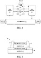
FIG. 4 illustrates, in block diagram form, a system for binding stacked die in accordance with another embodiment. -
FIG. 5 illustrates a cross-sectional view of a stacked die IC device in accordance with another embodiment. -
FIG. 6 illustrates a cross-sectional view of a stacked die IC device in accordance with another embodiment. -
FIG. 7 illustrates a top-down view of a stacked die IC device in accordance with another embodiment. - Generally, there is provided, an integrated circuit device having first and second semiconductor die, wherein the second semiconductor is stacked on the first semiconductor die. The second semiconductor die is attached, at least partially, to the first semiconductor die using a physically unclonable function (PUF). The PUF includes a plurality of conductive paths formed between the first semiconductor die and the second semiconductor die. A PUF controller is coupled to the PUF. The PUF controller generates a digital value based on an impedance of each of the plurality of conductive paths. The digital value is for binding the first semiconductor die to the second semiconductor die so that separating the first and second semiconductor die causes encrypted data stored on one of the die to become irretrievable.
- In one embodiment, there is provided, an integrated circuit device comprising: a first semiconductor die; a second semiconductor die attached, at least partially, to the first semiconductor die using a physically unclonable function (PUF) comprising a plurality of conductive paths formed between the first semiconductor die and the second semiconductor die; and a PUF controller, coupled to the PUF, for generating a digital value based on a characteristic of each conductor of the plurality of conductive paths, wherein the digital value is for binding the first semiconductor die to the second semiconductor die. The first semiconductor die may comprise a memory, and wherein the digital value may be characterized as being an encryption key for encoding data stored on the memory. The memory may be a nonvolatile memory used to provide a monotonic counter. The plurality of conductive paths may comprise a plurality of metal lines formed on a surface of the second semiconductor die, the plurality of metal lines being laid out to have substantially a same length. The integrated circuit device may further comprise: a plurality of line drivers coupled to a first end of the plurality of conductive paths; a plurality of line receivers coupled to a second end of the plurality of conductors; and a PUF controller coupled to the plurality of line drivers and to the plurality of line receivers, the PUF controller for measuring the characteristic of each of the plurality of conductive paths and calculating the digital value. Each conductor of the plurality of conductive paths may comprise a through silicon via (TSV) formed through the second semiconductor die. The integrated circuit device may further comprise a third semiconductor die. The characteristic may be an impedance of each conductor of the plurality of conductive paths. The plurality of conductive paths may further comprise a plurality of pads formed in a pattern on a surface of the first semiconductor die, and a plurality of pads formed in the pattern on a surface of the second semiconductor die so that the plurality of pads on both first and second semiconductor die align with each other and make electrical contact when the first semiconductor die is attached to the second semiconductor die, and wherein the first and second semiconductor die may be attached in misalignment to prevent electrical contact between at least some of the plurality of pads.
- In another embodiment, there is provided, an integrated circuit device comprising: a first semiconductor die comprising a nonvolatile memory; a second semiconductor die attached, at least partially, to the first semiconductor die using a physically unclonable function (PUF) comprising a plurality of conductive paths formed between the first semiconductor die and the second semiconductor die; and a PUF controller, coupled to the PUF, for generating an encryption key based on an impedance of each conductor of the plurality of conductive paths, wherein the encryption key is for encrypting data stored in the nonvolatile memory. The plurality of conductive paths may comprise one or more of a wire bond, through silicon via (TSV), or a solder ball. The first and second semiconductor die may be attached to each other in a stacked die arrangement. The integrated circuit device may further comprise a third semiconductor die. The plurality of conductive paths may further comprise a plurality of pads formed in a pattern on a surface of the first semiconductor die, and a plurality of pads formed in the pattern on a surface of the second semiconductor die so that the plurality of pads on both first and second semiconductor die align with each other and make electrical contact when the first semiconductor die is attached to the second semiconductor die, and wherein the first and second semiconductor die may be attached in misalignment to prevent electrical contact between at least some of the plurality of pads. The plurality of conductive paths may comprise a plurality of metal lines formed on a surface of the second semiconductor die, the plurality of metal lines being laid out to have substantially a same length.
- In yet another embodiment, there is provided, a method for logically binding first and second semiconductor die together for use in a security application, the method comprising: providing a plurality of first terminals on a surface of the first semiconductor die and a plurality of second terminals on a surface of the second semiconductor die; providing a plurality of conductors on the surface of the second semiconductor die, each end of the plurality of conductors coupled to a corresponding one of the plurality of second terminals; measuring a characteristic of each conductor of the plurality of conductors; and calculating a digital value based on the measured characteristics. The characteristic may be an impedance of each conductor. The first semiconductor die may comprise a nonvolatile memory and the digital value is an encryption key for encrypting data stored in the nonvolatile memory. All the plurality of conductors may be substantially the same length. Providing a plurality of first terminals may comprise forming the plurality of first terminals so that the plurality of first terminals aligns with the plurality of second terminals when the first and second semiconductor die are attached to each other. The method may further comprise misaligning the first and second semiconductor die to prevent electrical contact between at least some of the first plurality of terminals to corresponding terminals of the second plurality of terminals.
-
FIG. 1 illustrates a cross-sectional view of a stacked die integrated circuit (IC)device 10 in accordance with an embodiment.Integrated circuit device 10 includes semiconductor die 12 and semiconductor die 14. Semiconductor die 12 includes alayer 16 comprising active circuitry and interconnects.Layer 16 is formed in and onsemiconductor substrate 17. The active layer includes passive and active devices such as transistors, diodes, resistors, capacitors, and the like. The interconnects include alternating layers of patterned metal lines and insulating layers. The patterned metal lines are for conducting signals to components on and off the die. In one embodiment, thesemiconductor substrate 17 is formed from silicon and the active circuitry comprises non-volatile memory (NVM) cells formed in an array. In some embodiments, stacked die 12 and 14 may be packaged using an encapsulation material and conventional encapsulation techniques (not shown). Terminals may be provided for making electrical connections between semiconductor die 12 and 14 and other circuitry (not shown). The terminals may include, for example, an array of solder balls formed on pads, or leads from a lead frame. The NVM may include any type of NVM cell, such as for example, flash, EEPROM (electrically erasable programmable read only memory), MRAM (magnetic read only memory), and the like. The NVM may be used to store encrypted data, or may be used to provide a monotonic counter. Other circuitry may be formed in thelayer 16 from transistors formed using complementary metal-oxide semiconductor (CMOS) technology. In other embodiments, the technology and transistor types may be different. The interconnects include one or more layers comprising conductors formed from patterned metal such as copper and aluminum. The interconnects are for providing electrical communication of signals and power supply to the active circuitry and to communicate with other devices external to semiconductor die 12. Semiconductor die 14 includeslayer 20 comprising active circuitry and interconnects.Layer 20 is formed in and onsemiconductor substrate 22. In one embodiment, thesemiconductor substrate 17 is formed from silicon and the active circuitry comprises, for example, CMOS transistors for forming, for example, logic gates. In another embodiment, the transistor types may be different. Semiconductor die 12 and 14 are electrically connected using through silicon vias (TSVs) 18. The TSVs may be substituted for with wire bonds or solder balls in other embodiments. An embodiment having wire bonds is illustrated inFIG. 5 and will be discussed later. -
FIG. 2 illustrates a top down view of a surface of first semiconductor die 12 in accordance with an embodiment. A plurality ofterminals 24 are provided for electrically connecting the circuitry of active andmetal layers 16 to second semiconductor die 14. The plurality of terminals is formed on a surface ofsubstrate 17 on a side opposite active and metal layers 16. The plurality ofterminals 24 is connected to the active andmetal layers 16 byTSVs 18, illustrated inFIG. 1 , where oneTSV 18 corresponds to oneterminal 24. -
FIG. 3 illustrates a top-down view of a surface of semiconductor die 14 in accordance with an embodiment. A plurality ofterminals 26 is formed on a surface of active and metal layers 20. The plurality ofterminals 26 are positioned and arranged to correspond with the location and arrangement of plurality ofterminals 24 when semiconductor die 12 is stacked on semiconductor die 14. The plurality ofterminals 24 are then electrically connected with the plurality ofterminals 26. In one embodiment, solder or a conductive adhesive is used to make the electrical connections. A plurality ofmetal lines 28 are formed between pairs ofterminals 26. The plurality ofmetal lines 28 are laid out to have substantially the same lengths and widths. The plurality ofmetal lines 28 may be implemented in one of the interconnect layers of active andmetal lines 20 indie 14. Four metal lines are illustrated inFIG. 3 for purposes of simplicity and clarity. In one embodiment, the metal lines may be formed to provide an encryption key of 128 bits. Also, in another embodiment, the metal lines may be formed from another conductive material, such as for example, polysilicon. - When pluralities of
terminals metal layers 16 toterminal 24, to one end of aTSV 18, throughTSV 18 to a terminal 26 at theother end TSV 18 on semiconductor die 14. Then through ametal line 28 to another terminal 26, and through aTSV 18 to another terminal 24 on semiconductor die 12. - When the first and second semiconductor dies 12 and 14 are joined in a stacked die arrangement, the conductive paths together form a physically unclonable function (PUF). A physically unclonable function (PUF) is a physical system that will produce an unpredictable response when a stimulus is input. A PUF can be used to generate an encryption key because it is very difficult, or nearly impossible, to recreate. There are a number of ways to produce a PUF. One example uses the startup state of a static random access memory (SRAM). In the illustrated embodiment, the PUF includes a plurality of conductive paths having a plurality of parallel conductors. Each of the plurality of conductors has about the same laid out length and width. Even though the metal lines are substantially the same, impedance values for each of the lines will vary because of, for example, manufacturing variations and temperature changes. A characteristic of the plurality of metal lines, such as impedance, provides a digital value that can be used to generate, for example, an encryption key. In one embodiment, a relative impedance of each of the metal lines determines whether a logic one or a logic zero is provided by a metal line of the PUF. If the stacked die are separated, the impedance values of each of the plurality of conductive paths would be difficult to determine and reconstruct because the lines are laid out so that the differences in impedance values is relatively small and because the solder bonds in the conductive paths contribute to the difference in impedance. The solder bonds need to be destroyed to separate the dies and thus the contribution of the solder bonds to the total impedance of the conductive paths cannot be measured.
-
FIG. 4 illustrates, in block diagram form, a system for binding stacked die in accordance with another embodiment. The system includesline drivers 32 andline receivers 34 connected toPUF controller 30. In the illustrated embodiment, the system is implemented on semiconductor die 12. The conductive paths are illustrated connecting fromline drivers 32 to the plurality ofterminals 24,TSVs 18 and the plurality ofterminals 26,metal lines 28, plurality ofterminals 26, andline receivers 34. Only four conductive paths are illustrated for the purposes of simplicity and clarity. In an actual implementation, more conductive paths would be provided to create, for example, a 128-bit encryption key. Because the lines are laid out to be the same length and width, the impedances of the conductive paths between the two die will be relatively close to each other. If the two stacked die are separated, it would be unlikely an attacker could recreate the impedances of each of the metal lines so that the impedances would be the same as before being separated. - In one embodiment,
line drivers 32 provide a time varying signal at one end of themetal lines 28, andline receivers 34 comprise a termination circuit. A voltage or current, either measured over time or instantaneous and measured atline receivers 34, may be used to provide an impedance value for each metal line. The impedance would be compared to a reference impedance to determine if the metal line is providing a logic one or a logic zero. Alternately, a comparator or arbitration circuit coupled between two lines may be used to determine the logic states between two conductive paths. Also, the reference impedance may be provided by a selected one of the conductive paths in one embodiment. Alternately, the reference impedance may be provided by an adjacent conductive path, where an impedance of each conductive path is compared to an impedance of the adjacent conductive path. Other techniques for providing the reference may be used in other embodiments. Because the measured impedances may be different each time the device is powered up, helper data may be used to help recreate the cryptographic key from the PUF. The helper data may be stored in the NVM of semiconductor die 14 and is provided toPUF controller 30 to be used to generate the cryptographic key. The reconstructed cryptographic key is used to encrypt and decrypt data stored in the NVM. If the device is separated by an attacker, the helper data will be useless because the digital value from the PUF cannot be recreated. The algorithm used for the encryption can be any encryption algorithm, such as for example, advanced encryption standard (AES) or elliptic curve cryptography (ECC). -
FIG. 5 illustrates a cross-sectional view of stackeddie IC device 40 in accordance with another embodiment. Stackeddie IC device 40 includes semiconductor die 42 and semiconductor die 44. Semiconductor die 42 includes active andmetal layers 46 formed at a surface ofsubstrate 48, and semiconductor die 44 includes active andmetal layers 50 formed at a surface ofsubstrate 52. The active layers include passive and active devices such as transistors, diodes, resistors, capacitors, and the like. Stackeddie IC device 40 is the same as stackeddie IC device 10 except that TSVs 18 have been replaced with a plurality ofwire bonds 47 in the conductive paths that form the PUF. Preferably the bond wires are substantially the same length when attached to the dies 42 and 44. The use of wire bonds requires that wire bond pads be positioned on semiconductor die 44 so that they are exposed when semiconductor die 42 is attached to semiconductor die 44.Die FIG. 5 , the pads on semiconductor die 42 will not align with the pads of semiconductor die 44 as described in the embodiment ofFIG. 1 . -
FIG. 6 illustrates a cross-sectional view of a stackeddie IC device 60 in accordance with another embodiment. Stackeddie IC device 60 includes three semiconductor die. The three die may be encapsulated in accordance with known encapsulation techniques. As illustrated inFIG. 6 , semiconductor die 62 is the top die, semiconductor die 64 is the middle die, and semiconductor die 66 is the bottom die. Semiconductor die 62 includes active andmetal layers 64 formed onsubstrate 65. Semiconductor die 64 includes active andmetal layers 70 formed onsubstrate 72. Semiconductor die 66 includes active andmetal layers 74 formed onsubstrate 76. A plurality ofsolder balls 68 is used to electrically attach pads on the active surface ofdie 62 to pads on the active surface ofdie 64. A plurality ofTSVs 67 is used to route signals between the active surface ofdie 64 to the bottom surface ofdie 64. The plurality ofTSVs 67 may be used to electrically connect the active surface ofdie 64 to the active surface ofdie 66.Die 66 may include an NVM. In one embodiment, a PUF is formed having a plurality of conductive paths fromactive surface 70 throughTSVs 67 toactive layer 74 ofdie 66, where a plurality of metal lines is formed as shown inFIG. 3 , and the conductive path continues back throughTSVs 67 toactive surface 70 ofdie 64. Line drivers, line receivers, and a PUF controller, as illustrated inFIG. 4 , may be implemented onactive surface 70 ofdie 64. In another embodiment, the conductive paths for the PUF may extend through all three die. -
FIG. 7 illustrates a top-down view of astacked die IC 80 device in accordance with another embodiment.Stacked die IC 80 includes semiconductor die 81 attached to semiconductor die 82. Each die includes an array of pads or terminals on one surface that are at first positioned and sized to align with each other if the two die were to be stacked in alignment. In one embodiment, the pad arrangement may be in accordance with a Vernier scale. Generally, the conductive paths for forming the PUF are formed betweendie FIG. 7 , die 80 and 81 may be intentionally misaligned with each other to the extent that discontinuities are created between at least some of the pads in the PUF. Alternately, tiny misalignments due to the production process may be enough misalignment to create a wide variety of contact patterns over the array of pads. The pads can be very small and placed on the die with precision, limited only by the available lithographic patterning technology. It may be possible to detect very small misalignments in die placement. The misalignment is another physical characteristic which is difficult to recreate after the die are separated. However, the intentional misaligned for purposes of creating the PUF should not affect the connections between the die used for signaling and power distribution (not shown). This may be accomplished by making the PUF pads much smaller than the pads intended for signaling and power, so that a relatively small amount of misalignment of the die has the desired effect on the PUF without affecting functionality. The misalignment may include a rotational misalignment as illustrated inFIG. 7 , and a misalignment is the X and Y axis. The misalignment may prevent some of the pads on one die from contacting their counterpart pads on the other die. Also, the misalignment might reduce the area of the pads that contact with each other, thus introducing another variable for the resistance calculation in the corresponding conductive path. In addition, one pad on one die may touch two pads on the other die. Such effects may be accentuated with pad sizes and spacing that slightly violates the design rules for the given production process. As examples of the above cases,pads pads Pads Pads - Because the apparatus implementing the present invention is, for the most part, composed of electronic components and circuits known to those skilled in the art, circuit details will not be explained in any greater extent than that considered necessary as illustrated above, for the understanding and appreciation of the underlying concepts of the present invention and in order not to obfuscate or distract from the teachings of the present invention.
- Although the invention is described herein with reference to specific embodiments, various modifications and changes can be made without departing from the scope of the present invention as set forth in the claims below. Accordingly, the specification and figures are to be regarded in an illustrative rather than a restrictive sense, and all such modifications are intended to be included within the scope of the present invention. Any benefits, advantages, or solutions to problems that are described herein with regard to specific embodiments are not intended to be construed as a critical, required, or essential feature or element of any or all the claims. Generally, in the above described embodiment, a current electrode is a source or drain and a control electrode is a gate of a metal-oxide semiconductor (MOS) transistor. Other transistor types may be used in other embodiments.
- The term "coupled," as used herein, is not intended to be limited to a direct coupling or a mechanical coupling.
- Furthermore, the terms "a" or "an," as used herein, are defined as one or more than one. Also, the use of introductory phrases such as "at least one" and "one or more" in the claims should not be construed to imply that the introduction of another claim element by the indefinite articles "a" or "an" limits any particular claim containing such introduced claim element to inventions containing only one such element, even when the same claim includes the introductory phrases "one or more" or "at least one" and indefinite articles such as "a" or "an." The same holds true for the use of definite articles.
- Unless stated otherwise, terms such as "first" and "second" are used to arbitrarily distinguish between the elements such terms describe. Thus, these terms are not necessarily intended to indicate temporal or other prioritization of such elements.
Claims (14)
- An integrated circuit device comprising:a first semiconductor die;a second semiconductor die attached, at least partially, to the first semiconductor die using a physically unclonable function (PUF) comprising a plurality of conductive paths formed between the first semiconductor die and the second semiconductor die; anda PUF controller, coupled to the PUF, for generating a digital value based on a characteristic of each conductor of the plurality of conductive paths, wherein the digital value is for binding the first semiconductor die to the second semiconductor die.
- The integrated circuit device of claim 1, wherein the first semiconductor die comprises a memory, and wherein the digital value is characterized as being an encryption key for encrypting data stored on the memory.
- The integrated circuit device of claim 2, wherein the memory is a nonvolatile memory used to provide a monotonic counter.
- The integrated circuit device of any preceding claim, wherein the plurality of conductive paths comprises a plurality of metal lines formed on a surface of the second semiconductor die, the plurality of metal lines being laid out to have substantially a same length.
- The integrated circuit device of any preceding claim, further comprising:a plurality of line drivers coupled to a first end of the plurality of conductive paths;a plurality of line receivers coupled to a second end of the plurality of conductors; anda PUF controller coupled to the plurality of line drivers and to the plurality of line receivers, the PUF controller for measuring the characteristic of each of the plurality of conductive paths and calculating the digital value.
- The integrated circuit device of claim 5, wherein each conductor of the plurality of conductive paths comprises a through silicon via (TSV) formed through the second semiconductor die.
- The integrated circuit device of any preceding claim, further comprising a third semiconductor die.
- The integrated circuit device of any preceding claim, wherein the characteristic is an impedance of each conductor of the plurality of conductive paths.
- The integrated circuit device of any preceding claim, wherein the plurality of conductive paths further comprises a plurality of pads formed in a pattern on a surface of the first semiconductor die, and a plurality of pads formed in the pattern on a surface of the second semiconductor die so that the plurality of pads on both first and second semiconductor die align with each other and make electrical contact when the first semiconductor die is attached to the second semiconductor die, and wherein the first and second semiconductor die are attached in misalignment to prevent electrical contact between at least some of the plurality of pads.
- A method for logically binding first and second semiconductor die together for use in a security application, the method comprising:providing a plurality of first terminals on a surface of the first semiconductor die and a plurality of second terminals on a surface of the second semiconductor die;providing a plurality of conductors on the surface of the second semiconductor die, each end of the plurality of conductors coupled to a corresponding one of the plurality of second terminals;measuring a characteristic of each conductor of the plurality of conductors; andcalculating a digital value based on the measured characteristics.
- The method of claim 10, wherein the characteristic is an impedance of each conductor.
- The method of claim 10 or 11, wherein the first semiconductor die comprises a nonvolatile memory and the digital value is an encryption key for encrypting data stored in the nonvolatile memory.
- The method of any one of claims 10 to 12, wherein all the plurality of conductors is substantially the same length.
- The method of any one of claims 10 to 13, wherein providing a plurality of first terminals comprises forming the plurality of first terminals so that the plurality of first terminals aligns with the plurality of second terminals when the first and second semiconductor die are attached to each other, and wherein the method further comprising misaligning the first and second semiconductor die to prevent electrical contact between at least some of the first plurality of terminals to corresponding terminals of the second plurality of terminals.
Applications Claiming Priority (1)
| Application Number | Priority Date | Filing Date | Title |
|---|---|---|---|
| US15/451,589 US10547461B2 (en) | 2017-03-07 | 2017-03-07 | Method and apparatus for binding stacked die using a physically unclonable function |
Publications (1)
| Publication Number | Publication Date |
|---|---|
| EP3373511A1 true EP3373511A1 (en) | 2018-09-12 |
Family
ID=61132034
Family Applications (1)
| Application Number | Title | Priority Date | Filing Date |
|---|---|---|---|
| EP18154146.7A Withdrawn EP3373511A1 (en) | 2017-03-07 | 2018-01-30 | Method and apparatus for binding stacked die using a physically unclonable function |
Country Status (2)
| Country | Link |
|---|---|
| US (1) | US10547461B2 (en) |
| EP (1) | EP3373511A1 (en) |
Cited By (1)
| Publication number | Priority date | Publication date | Assignee | Title |
|---|---|---|---|---|
| US20240413099A1 (en) * | 2023-06-08 | 2024-12-12 | Xilinx, Inc. | Multi-die physically unclonable function entropy source |
Families Citing this family (6)
| Publication number | Priority date | Publication date | Assignee | Title |
|---|---|---|---|---|
| EP3690867B1 (en) * | 2019-01-30 | 2025-06-11 | Siemens Aktiengesellschaft | Fingerprinting of semiconductor die arrangements |
| US11239414B2 (en) | 2020-03-24 | 2022-02-01 | International Business Machines Corporation | Physical unclonable function for MRAM structures |
| CN112653696B (en) * | 2020-12-22 | 2023-10-10 | 深圳市国微电子有限公司 | A security authentication system and method for 3D stacked chips |
| CN112667990A (en) * | 2020-12-22 | 2021-04-16 | 深圳市国微电子有限公司 | 3D stacked chip PUF (physical unclonable function) safety authentication system and method based on TSV design |
| US12177343B2 (en) * | 2021-06-25 | 2024-12-24 | Intel Corporation | Methods and apparatuses to provide chiplet binding to a system on a chip platform having a disaggregated architecture |
| US12408265B2 (en) | 2023-06-26 | 2025-09-02 | Nxp B.V. | Integrated circuit and method for detecting tampering of a printed circuit board |
Citations (5)
| Publication number | Priority date | Publication date | Assignee | Title |
|---|---|---|---|---|
| US20020051401A1 (en) * | 2000-10-25 | 2002-05-02 | Samsung Electronics Co., Ltd. | Semiconductor memory architecture for minimizing input/output data paths |
| WO2007063475A2 (en) * | 2005-11-29 | 2007-06-07 | Koninklijke Philips Electronics N.V. | Proofs of vicinity using cpufs |
| US20110234241A1 (en) * | 2009-02-23 | 2011-09-29 | Lewis James M | Method and system for protecting products and technology from integrated circuits which have been subject to tampering, stressing and replacement as well as detecting integrated circuits that have been subject to tampering |
| US20130320560A1 (en) * | 2012-05-29 | 2013-12-05 | Rambus Inc. | Distributed on-chip decoupling apparatus and method using package interconnect |
| US20140157404A1 (en) * | 2012-11-30 | 2014-06-05 | Siddhartha Chhabra | Virtualizing a hardware monotonic counter |
Family Cites Families (23)
| Publication number | Priority date | Publication date | Assignee | Title |
|---|---|---|---|---|
| AT3919U3 (en) * | 2000-07-13 | 2001-08-27 | Plasser Bahnbaumasch Franz | MACHINE FOR DISMANTLING AN OLD AND LAYING A NEW TRACK |
| DE10044837C1 (en) | 2000-09-11 | 2001-09-13 | Infineon Technologies Ag | Circuit arrangement and method for detecting an unwanted attack on an integrated circuit |
| DE10223176B3 (en) | 2002-05-24 | 2004-01-22 | Infineon Technologies Ag | Integrated circuit with safety-critical circuit components |
| FR2864667B1 (en) | 2003-12-29 | 2006-02-24 | Commissariat Energie Atomique | PROTECTING AN INTEGRATED CIRCUIT CHIP CONTAINING CONFIDENTIAL DATA |
| EP1721231B1 (en) | 2004-02-24 | 2009-12-23 | Nxp B.V. | Method and apparatus for protecting an integrated circuit using an intrusion detection by Monte Carlo analysis |
| US8074082B2 (en) * | 2004-10-08 | 2011-12-06 | Aprolase Development Co., Llc | Anti-tamper module |
| EP2615641B1 (en) | 2006-01-24 | 2015-07-01 | Nds Limited | Chip attack protection |
| KR20080011829A (en) | 2006-07-31 | 2008-02-11 | 삼성전자주식회사 | Organic electroluminescent display and manufacturing method thereof |
| WO2008102282A2 (en) | 2007-02-20 | 2008-08-28 | Nxp B.V. | Semiconductor device with backside tamper protection |
| CN101772775B (en) | 2007-08-02 | 2013-07-10 | Nxp股份有限公司 | Tamper-resistant semiconductor device and method of manufacturing the tamper-resistant semiconductor device |
| CN101828261B (en) | 2007-10-18 | 2012-05-23 | Nxp股份有限公司 | Magnetic detection of the backside layer |
| KR101046388B1 (en) * | 2009-06-15 | 2011-07-05 | 주식회사 하이닉스반도체 | Semiconductor package |
| WO2011018414A2 (en) | 2009-08-14 | 2011-02-17 | Intrinsic Id B.V. | Physically unclonable function with tamper prevention and anti-aging system |
| US20130141137A1 (en) * | 2011-06-01 | 2013-06-06 | ISC8 Inc. | Stacked Physically Uncloneable Function Sense and Respond Module |
| EP2665094A1 (en) | 2012-05-15 | 2013-11-20 | Nxp B.V. | Tamper resistant IC |
| EP2875156A4 (en) * | 2012-07-19 | 2016-02-24 | Ariosa Diagnostics Inc | DETECTION BASED ON MULTIPLEX SEQUENTIAL LIGATION OF GENETIC VARIANTS |
| US8759976B2 (en) | 2012-08-09 | 2014-06-24 | International Business Machines Corporation | Structure with sub-lithographic random conductors as a physical unclonable function |
| US20140042627A1 (en) | 2012-08-09 | 2014-02-13 | International Business Machines Corporation | Electronic structure containing a via array as a physical unclonable function |
| KR20140034332A (en) | 2012-08-14 | 2014-03-20 | 삼성전자주식회사 | Security device and integrated circuit having the same |
| JP5954872B2 (en) | 2012-09-20 | 2016-07-20 | ルネサスエレクトロニクス株式会社 | Semiconductor integrated circuit |
| US9053317B2 (en) * | 2013-02-28 | 2015-06-09 | Winbond Electronics Corporation | Nonvolatile memory device having authentication, and methods of operation and manufacture thereof |
| DE102013205729A1 (en) * | 2013-03-28 | 2014-10-02 | Fraunhofer-Gesellschaft zur Förderung der angewandten Forschung e.V. | Device and method with a carrier with circuit structures |
| US10452872B2 (en) * | 2016-05-26 | 2019-10-22 | Raytheon Company | Detection system for detecting changes to circuitry and method of using the same |
-
2017
- 2017-03-07 US US15/451,589 patent/US10547461B2/en not_active Expired - Fee Related
-
2018
- 2018-01-30 EP EP18154146.7A patent/EP3373511A1/en not_active Withdrawn
Patent Citations (5)
| Publication number | Priority date | Publication date | Assignee | Title |
|---|---|---|---|---|
| US20020051401A1 (en) * | 2000-10-25 | 2002-05-02 | Samsung Electronics Co., Ltd. | Semiconductor memory architecture for minimizing input/output data paths |
| WO2007063475A2 (en) * | 2005-11-29 | 2007-06-07 | Koninklijke Philips Electronics N.V. | Proofs of vicinity using cpufs |
| US20110234241A1 (en) * | 2009-02-23 | 2011-09-29 | Lewis James M | Method and system for protecting products and technology from integrated circuits which have been subject to tampering, stressing and replacement as well as detecting integrated circuits that have been subject to tampering |
| US20130320560A1 (en) * | 2012-05-29 | 2013-12-05 | Rambus Inc. | Distributed on-chip decoupling apparatus and method using package interconnect |
| US20140157404A1 (en) * | 2012-11-30 | 2014-06-05 | Siddhartha Chhabra | Virtualizing a hardware monotonic counter |
Cited By (2)
| Publication number | Priority date | Publication date | Assignee | Title |
|---|---|---|---|---|
| US20240413099A1 (en) * | 2023-06-08 | 2024-12-12 | Xilinx, Inc. | Multi-die physically unclonable function entropy source |
| US12564062B2 (en) * | 2023-06-08 | 2026-02-24 | Xilinx, Inc. | Multi-die physically unclonable function entropy source |
Also Published As
| Publication number | Publication date |
|---|---|
| US20180262353A1 (en) | 2018-09-13 |
| US10547461B2 (en) | 2020-01-28 |
Similar Documents
| Publication | Publication Date | Title |
|---|---|---|
| US10547461B2 (en) | Method and apparatus for binding stacked die using a physically unclonable function | |
| TWI882813B (en) | Multichip package comprising a standard commodity fpga ic chip with cryptography circuits | |
| US20250316607A1 (en) | Logic drive based on multichip package comprising standard commodity fpga ic chip with cooperating or supporting circuits | |
| US20230137364A1 (en) | Packaging techniques for backside mesh connectivity | |
| US12482800B2 (en) | Semiconductor package including processor chip and memory chip | |
| TWI672787B (en) | Semiconductor packages with interposers and methods of manufacturing the same | |
| TW577152B (en) | Semiconductor integrated circuit device | |
| US20150129978A1 (en) | Semiconductor integrated circuit, method for fabricating the same, and semiconductor package | |
| CN107112301A (en) | Integration of electronic components on the backside of a semiconductor chip | |
| US20080272478A1 (en) | Circuit and method for interconnecting stacked integrated circuit dies | |
| US9667410B2 (en) | Semiconductor device | |
| KR102085973B1 (en) | Test circuit of semiconductor device and test method of semiconductor device | |
| EP2462614A4 (en) | ENCAPSULATED SEMICONDUCTOR DEVICE FOR MEMORY AND HIGH PERFORMANCE LOGIC | |
| WO2010104543A2 (en) | Integrated circuits secure from invasion and methods of manufacturing the same | |
| US7715227B2 (en) | Programmable ROM using two bonded strata | |
| TW201010034A (en) | Semiconductor memory device having pads | |
| CN106206557A (en) | Silicon Interposer | |
| CN114342074A (en) | Integrated circuit arrangement with a capacitor | |
| CN106098659B (en) | Semiconductor device | |
| US8754518B1 (en) | Devices and methods for configuring conductive elements for a semiconductor package | |
| TWI916212B (en) | Multichip package comprising a standard commodity fpga ic chip with cryptography circuits | |
| KR20230031713A (en) | Semiconductor package | |
| CN114078796A (en) | Semiconductor package including stacked semiconductor chips | |
| TW202610076A (en) | Semiconductor package | |
| CN108008933A (en) | A kind of circuit of random sequence number for being used to produce chip and the chip including the circuit |
Legal Events
| Date | Code | Title | Description |
|---|---|---|---|
| PUAI | Public reference made under article 153(3) epc to a published international application that has entered the european phase |
Free format text: ORIGINAL CODE: 0009012 |
|
| STAA | Information on the status of an ep patent application or granted ep patent |
Free format text: STATUS: THE APPLICATION HAS BEEN PUBLISHED |
|
| AK | Designated contracting states |
Kind code of ref document: A1 Designated state(s): AL AT BE BG CH CY CZ DE DK EE ES FI FR GB GR HR HU IE IS IT LI LT LU LV MC MK MT NL NO PL PT RO RS SE SI SK SM TR |
|
| AX | Request for extension of the european patent |
Extension state: BA ME |
|
| STAA | Information on the status of an ep patent application or granted ep patent |
Free format text: STATUS: REQUEST FOR EXAMINATION WAS MADE |
|
| 17P | Request for examination filed |
Effective date: 20190312 |
|
| RBV | Designated contracting states (corrected) |
Designated state(s): AL AT BE BG CH CY CZ DE DK EE ES FI FR GB GR HR HU IE IS IT LI LT LU LV MC MK MT NL NO PL PT RO RS SE SI SK SM TR |
|
| STAA | Information on the status of an ep patent application or granted ep patent |
Free format text: STATUS: EXAMINATION IS IN PROGRESS |
|
| 17Q | First examination report despatched |
Effective date: 20210406 |
|
| STAA | Information on the status of an ep patent application or granted ep patent |
Free format text: STATUS: THE APPLICATION IS DEEMED TO BE WITHDRAWN |
|
| 18D | Application deemed to be withdrawn |
Effective date: 20240801 |