EP3373448A1 - Radio frequency circuits and methods of processing radio frequency signals - Google Patents
Radio frequency circuits and methods of processing radio frequency signals Download PDFInfo
- Publication number
- EP3373448A1 EP3373448A1 EP17275035.8A EP17275035A EP3373448A1 EP 3373448 A1 EP3373448 A1 EP 3373448A1 EP 17275035 A EP17275035 A EP 17275035A EP 3373448 A1 EP3373448 A1 EP 3373448A1
- Authority
- EP
- European Patent Office
- Prior art keywords
- signal
- circuit
- phase noise
- output
- frequency oscillator
- Prior art date
- Legal status (The legal status is an assumption and is not a legal conclusion. Google has not performed a legal analysis and makes no representation as to the accuracy of the status listed.)
- Ceased
Links
Images


Classifications
-
- H—ELECTRICITY
- H03—ELECTRONIC CIRCUITRY
- H03D—DEMODULATION OR TRANSFERENCE OF MODULATION FROM ONE CARRIER TO ANOTHER
- H03D7/00—Transference of modulation from one carrier to another, e.g. frequency-changing
-
- H—ELECTRICITY
- H04—ELECTRIC COMMUNICATION TECHNIQUE
- H04B—TRANSMISSION
- H04B1/00—Details of transmission systems, not covered by a single one of groups H04B3/00 - H04B13/00; Details of transmission systems not characterised by the medium used for transmission
- H04B1/02—Transmitters
- H04B1/04—Circuits
- H04B1/0475—Circuits with means for limiting noise, interference or distortion
-
- H—ELECTRICITY
- H03—ELECTRONIC CIRCUITRY
- H03B—GENERATION OF OSCILLATIONS, DIRECTLY OR BY FREQUENCY-CHANGING, BY CIRCUITS EMPLOYING ACTIVE ELEMENTS WHICH OPERATE IN A NON-SWITCHING MANNER; GENERATION OF NOISE BY SUCH CIRCUITS
- H03B2200/00—Indexing scheme relating to details of oscillators covered by H03B
- H03B2200/006—Functional aspects of oscillators
- H03B2200/0088—Reduction of noise
- H03B2200/009—Reduction of phase noise
Definitions
- the present invention concerns radio frequency circuits and methods of processing radio frequency signals. More particularly, but not exclusively, the invention concerns radio receiver circuits, radio transmitter circuits and the like.
- variable frequency oscillator system In radio frequency circuits such as radio receivers and the like, a variable frequency oscillator system is often used to feed a frequency mixer or digitising component in order to process a radio frequency signal.
- variable frequency oscillator systems are prone to phase noise, which relates to the variable frequency oscillator system's short term frequency stability (i.e. fluctuation in the phase of the waveform of the oscillating signal produced by the variable frequency oscillator system).
- This phase noise can have a significant effect upon the operation of the radio receiver, as it is transferred to the product of the radio frequency signal and the variable frequency oscillator system (e.g. when the signals are combined by the frequency mixer).
- Figure 1 shows a circuit diagram of a part of a known radio frequency receiver circuit.
- the circuit comprises a mixer 4, a variable frequency oscillator system 2 and a filter 6.
- the variable frequency oscillator system 2 outputs an oscillating signal 3 to the mixer 4.
- the mixer 4 then combines the oscillating signal 3 with a received radio frequency signal 1 to generate a product signal 5.
- the product signal 5 is passed through a filter 6 (for example, a low pass filter) to produce a filtered signal 7, which continues to further stages 8 in the radio receiver where it is processed.
- the oscillating signal 3 of the variable frequency oscillator system 2 is prone to phase noise, which is carried through to the product signal 5. This product signal 5 can therefore result in degraded radio performance due to the contamination of the radio frequency signal.
- variable frequency oscillator system In order to reduce the disadvantageous effects of phase noise, high-specification components can be used to construct the variable frequency oscillator system. However, particularly at microwave and ultrahigh frequencies, such components can be very expensive and/or bulky. Techniques include the use of yttrium iron garnet (YIG) oscillators, switched banks of narrow-tuning-range oscillators, and the coherent summation of two or more oscillators.
- YIG yttrium iron garnet
- the present invention seeks to mitigate the above-mentioned problems. Alternatively and/or additionally, the present invention seeks to provide improved radio frequency circuits and methods of processing radio frequency signals.
- a radio frequency circuit for processing a radio frequency signal comprising:
- the processing of the output radio frequency signal can be done digitally, using any desired digital processing method. Further, by capturing the phase noise in the output of the variable frequency oscillator system and using this when digitally processing the digitised signal, the digital processing can be done to compensate for the effect of the phase noise. In this way, rather than minimising the phase noise present in the variable frequency oscillator system signal, which can require the use of expensive and/or bulky components, a "lower quality" variable frequency oscillator system can be used in which phase noise is present, and then any disadvantageous effects on the output radio frequency signal due to that phase noise can be removed (or at least mitigated) by the digital processing. Further, such digital processing method can be as complicated as desired in order to achieve the best possible result, without expensive and/or bulky components being required digitisers are commonly used for many applications and so are easily and cheaply available.
- the phase noise capture circuit comprises a fixed frequency oscillator.
- Fixed frequency oscillators are available that can generate an oscillating signal with very little phase noise, without expensive and/or bulky components being required.
- the variable frequency oscillator system may be arranged to use the output of the fixed frequency oscillator.
- the variable frequency oscillator system may use the output of the fixed frequency oscillator as a reference to generate the variable frequency signal, for example.
- the digitiser may be arranged to receive the output of the fixed frequency oscillator. The digitiser may use the output of the fixed frequency oscillator to generate its sampling clock, for example.
- the phase noise capture circuit may further comprise: a comb generator arranged to receive the output of the fixed frequency oscillator and generate a signal comprising harmonics of the output of the fixed frequency oscillator; a mixer arranged to mix the output of the comb generator with the output of the variable frequency oscillator system; and a low pass filter arranged to filter the output of the mixer.
- the phase noise is transferred to a low frequency signal, as the low pass filter will only pass the part of the output of the mixer that is generated by subtracting from the variable frequency oscillator system signal the closest harmonic of the fixed frequency oscillator signal from the comb generator, so that it is lower than the threshold of the low pass filter.
- phase noise capture circuit may be arranged to measure the phase noise in the output of the variable frequency oscillator system.
- the circuit may further comprise a second digitiser arranged to receive the output of the phase noise capture circuit and generate a digitised signal.
- the circuit is a radio receiver circuit.
- the radio receiver circuit may be a superheterodyne receiver circuit.
- the circuit is a radio transmitter circuit.
- the circuit could be any other type of radio frequency circuit.
- the radio frequency signal processing circuit may be the whole of the circuit, or only a part thereof with other processing stages following the digital processing to compensate for the effect of the phase noise.
- the radio frequency signal may be a microwave frequency signal.
- the phase noise is captured using a fixed frequency oscillator signal.
- the variable frequency oscillator system may use the fixed frequency oscillator signal.
- the fixed frequency oscillator signal may be used to generating the digitised signal from the processed radio frequency signal. Capturing the phase noise may comprise the steps of:
- capturing the phase noise may comprise measuring the phase noise.
- the method may further comprise the step of generating a digitised signal from the captured phase noise, using a second digitiser.
- the radio frequency signal may be a microwave frequency signal.
- FIG 2 is a circuit diagram of a part of a radio frequency receiver circuit in accordance with an embodiment of the invention.
- the radio frequency receiver circuit 100 comprises a mixer 104, a variable frequency oscillator system 102 and a filter 106.
- the variable frequency oscillator system 102 again outputs an oscillating signal 103 to the mixer 104.
- the mixer 104 combines the oscillating signal 103 with a received radio frequency signal 101 to again generate a product signal 105.
- the product signal 105 is passed through a filter 106 (configured to perform desirable filtering, for example a low pass filter), to produce a filtered signal 107.
- a filter 106 configured to perform desirable filtering, for example a low pass filter
- the filtered signal 107 is then passed to an analogue to digital converter 210, which converts it into a digitised signal 211.
- the radio frequency receiver circuit 100 further comprises a phase noise capture circuit 208.
- the oscillating signal 103 of the variable frequency oscillator system 102 is also passed to the phase noise capture circuit 208.
- the phase noise capture circuit 208 measures the phase noise in the oscillating signal 103, and generates a phase noise signal 209 indicative of the phase noise in the oscillating signal 103.
- phase noise capture circuits of different types could be used.
- the oscillating signal 103 could be digitised and then digitally processed to determine the phase noise in the oscillating signal 103, and the phase noise capture circuit could then generate a digital signal indicative of the phase noise as the phase noise signal 209.
- the phase noise could be measured by analogue means.
- the phase noise capture circuit transfers it to a low frequency signal.
- phase noise compensation circuit 212 digitally processes the digitised signal 211, using the information provided by the phase noise signal 209, to compensate for any undesirable effects of the phase noise. It will be appreciated that this compensation could be done using various different techniques, either alone or in combination. For example, in a calibration phase the circuit could be fed test signals, to allow the effects of phase noise and how they could be compensated for to be determined. In another example, statistical methods could be used. It will be appreciated that as the digitised signal 211 is being processed digitally, very complicated techniques could be used, individually or together, without complicated and/or circuitry being required.
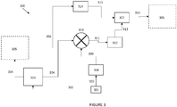
- FIG. 3 is a circuit diagram of a part of radio frequency receiver circuit including a phase noise capture circuit according to another embodiment of the invention.
- the radio frequency receiver circuit 300 comprises a fixed frequency oscillator 301, which generates a fixed frequency oscillating signal 302.
- the fixed frequency oscillator 301 may for example be a crystal oscillator, producing a signal at 100 MHz for example. Because only a fixed frequency oscillating signal is required, the fixed frequency oscillator 301 is able to generate an oscillating signal with very little phase noise, without expensive and/or bulky components being required.
- the fixed frequency oscillating signal 302 is passed to a variable frequency oscillator system circuit 303, which uses it to generate an oscillating signal 304 at the required frequency for a part 305 of the radio frequency receiver circuit 300 proper, for example an initial receiver stage that initially receives and processes the input radio frequency signal.
- the oscillating signal 304 from the variable frequency oscillator system circuit 303 will be prone to phase noise.
- the oscillating signal 304 is then passed to radio receiver circuitry 305, which uses it as required to generate an output signal 306.
- the radio receiver circuitry 305 may be the initial stage of a superhet receiver circuit, which takes an input radio frequency signal and generates an intermediate frequency signal as the output signal 306.
- the output signal 306 is then passed to an analogue to digital converter 210, which converts it into a digitised signal 315.
- the digitised signal 315 is then passed to a phase noise compensation circuit 307, which is discussed in more detail below.
- the radio frequency receiver circuit 300 also comprises a comb generator 308, which also receives the fixed frequency oscillating signal 302 from the fixed frequency oscillator 301.
- the comb generator 308 may for example comprise an amplifier and a fast non-linear device such as a step-recovery diode, though it will be appreciated that many ways of providing a comb generator will be known.
- the comb generator 308 generates a comb signal 309 comprising harmonics of the fixed frequency oscillating signal 302 (the harmonics providing the spikes in the "comb” seen in the frequency graph of the comb signal 309 generated by the comb generator 308). In other embodiments, other types of high-speed impulse generators may be used.
- the comb signal 309 from the comb generator 308 and the oscillating signal 304 from the variable frequency oscillator system 303 are then mixed by a frequency mixer 310, to produce a product signal 311.
- a sampling gate may be used.
- the product signal 311 is then passed to a low pass filter 312, which filters the product signal 311 to produce a filtered signal 313.
- the low pass filter 312 filters the product signal 311 so that the only part of the product signal 311 that remains is that produced by the oscillating signal 304 from which the closest frequency harmonic of the comb signal 309 has been subtracted.
- the filtered signal 313 comprises the phase noise in the oscillating signal 304 transferred to a low frequency signal.
- the fixed frequency oscillator 301, comb generator 308, frequency mixer 310 and low pass filter 312 provide a phase noise capture circuit that captures the phase noise in the oscillating signal 304.
- the filtered signal 313 is then passed to the phase noise compensation circuit 307, which uses the filtered signal 313 to digitally process the digitised signal 315 produced by digitising the output signal 307 from the radio receiver circuitry 305, to compensate for any undesirable effects of the phase noise.
- the compensation is done using the filtered signal 313 in which the phase noise in the oscillating signal 304 has been captured. As with the previous embodiment, this compensation could be done using various different techniques, either alone or in combination, and may involve the filtered signal 313 also being digitised.
- radio frequency receiver circuits While the above-described embodiments are radio frequency receiver circuits, it will be appreciated that the invention could be applied to other types of radio frequency circuits that use an oscillating signal that includes phase noise, for example a radio frequency transmitter circuit.
- the extraction of the phase noise from the oscillating signal requires a delay in processing. This is not a problem in a digital receiver, as there is also a delay in the receiver processing. It can be ensured that the measured noise is used to compensate the correct part of the received signal by equalising the delays, which is easily done in digitised signals. In other types of circuit such as a transmitter, it again is necessary to ensure that the measured noise is used to correct the correct part of circuit signal. In a transmitter this may be done, for example, by delaying the oscillating signal from the variable frequency oscillator system after the phase noise has been captured but before it is mixed with a signal.
Landscapes
- Engineering & Computer Science (AREA)
- Power Engineering (AREA)
- Computer Networks & Wireless Communication (AREA)
- Signal Processing (AREA)
- Noise Elimination (AREA)
Abstract
A radio frequency circuit for processing a radio frequency signal. The circuit comprises a variable frequency oscillator system and a radio frequency signal processing circuit arranged to process a radio frequency signal using the output of the variable frequency oscillator system. A digitiser is arranged to receive the output of the radio frequency signal processing circuit and generate a digitised signal. A phase noise capture circuit is arranged to capture the phase noise in the output of the variable frequency oscillator system. The radio frequency circuit is arranged to compensate for the effect of the phase noise in the output of the variable frequency oscillator system on the output of the radio frequency signal processing circuit, by digitally processing the digitised signal generated by the digitiser using the output of the phase noise capture circuit.
Description
- The present invention concerns radio frequency circuits and methods of processing radio frequency signals. More particularly, but not exclusively, the invention concerns radio receiver circuits, radio transmitter circuits and the like.
- In radio frequency circuits such as radio receivers and the like, a variable frequency oscillator system is often used to feed a frequency mixer or digitising component in order to process a radio frequency signal. However, variable frequency oscillator systems are prone to phase noise, which relates to the variable frequency oscillator system's short term frequency stability (i.e. fluctuation in the phase of the waveform of the oscillating signal produced by the variable frequency oscillator system). This phase noise can have a significant effect upon the operation of the radio receiver, as it is transferred to the product of the radio frequency signal and the variable frequency oscillator system (e.g. when the signals are combined by the frequency mixer).
-
Figure 1 shows a circuit diagram of a part of a known radio frequency receiver circuit. The circuit comprises a mixer 4, a variablefrequency oscillator system 2 and afilter 6. In operation, the variablefrequency oscillator system 2 outputs anoscillating signal 3 to the mixer 4. The mixer 4 then combines the oscillatingsignal 3 with a receivedradio frequency signal 1 to generate aproduct signal 5. Theproduct signal 5 is passed through a filter 6 (for example, a low pass filter) to produce a filteredsignal 7, which continues to furtherstages 8 in the radio receiver where it is processed. In such a circuit, the oscillatingsignal 3 of the variablefrequency oscillator system 2 is prone to phase noise, which is carried through to theproduct signal 5. Thisproduct signal 5 can therefore result in degraded radio performance due to the contamination of the radio frequency signal. - In order to reduce the disadvantageous effects of phase noise, high-specification components can be used to construct the variable frequency oscillator system. However, particularly at microwave and ultrahigh frequencies, such components can be very expensive and/or bulky. Techniques include the use of yttrium iron garnet (YIG) oscillators, switched banks of narrow-tuning-range oscillators, and the coherent summation of two or more oscillators.
- The present invention seeks to mitigate the above-mentioned problems. Alternatively and/or additionally, the present invention seeks to provide improved radio frequency circuits and methods of processing radio frequency signals.
- In accordance with a first aspect of the invention there is provided a radio frequency circuit for processing a radio frequency signal, comprising:
- a variable frequency oscillator system;
- a radio frequency signal processing circuit arranged to process a radio frequency signal using the output of the variable frequency oscillator system;
- a digitiser arranged to receive the output of the radio frequency signal processing circuit and generate a digitised signal;
- a phase noise capture circuit arranged to capture the phase noise in the output of the variable frequency oscillator system;
- wherein the radio frequency circuit is arranged to compensate for the effect of the phase noise in the output of the variable frequency oscillator system on the output of the radio frequency signal processing circuit, by digitally processing the digitised signal generated by the digitiser using the output of the phase noise capture circuit.
- By using a digitiser to generate a digitised signal from the output of the radio frequency signal processing circuit, the processing of the output radio frequency signal can be done digitally, using any desired digital processing method. Further, by capturing the phase noise in the output of the variable frequency oscillator system and using this when digitally processing the digitised signal, the digital processing can be done to compensate for the effect of the phase noise. In this way, rather than minimising the phase noise present in the variable frequency oscillator system signal, which can require the use of expensive and/or bulky components, a "lower quality" variable frequency oscillator system can be used in which phase noise is present, and then any disadvantageous effects on the output radio frequency signal due to that phase noise can be removed (or at least mitigated) by the digital processing. Further, such digital processing method can be as complicated as desired in order to achieve the best possible result, without expensive and/or bulky components being required digitisers are commonly used for many applications and so are easily and cheaply available.
- Preferably, the phase noise capture circuit comprises a fixed frequency oscillator. Fixed frequency oscillators are available that can generate an oscillating signal with very little phase noise, without expensive and/or bulky components being required. In the case the phase noise capture circuit comprises a fixed frequency oscillator, the variable frequency oscillator system may be arranged to use the output of the fixed frequency oscillator. The variable frequency oscillator system may use the output of the fixed frequency oscillator as a reference to generate the variable frequency signal, for example. Similarly, the digitiser may be arranged to receive the output of the fixed frequency oscillator. The digitiser may use the output of the fixed frequency oscillator to generate its sampling clock, for example.
- When the phase noise capture circuit comprises a fixed frequency oscillator, the phase noise capture circuit may further comprise: a comb generator arranged to receive the output of the fixed frequency oscillator and generate a signal comprising harmonics of the output of the fixed frequency oscillator; a mixer arranged to mix the output of the comb generator with the output of the variable frequency oscillator system; and a low pass filter arranged to filter the output of the mixer. In this way, the phase noise is transferred to a low frequency signal, as the low pass filter will only pass the part of the output of the mixer that is generated by subtracting from the variable frequency oscillator system signal the closest harmonic of the fixed frequency oscillator signal from the comb generator, so that it is lower than the threshold of the low pass filter.
- Alternatively, the phase noise capture circuit may be arranged to measure the phase noise in the output of the variable frequency oscillator system.
- The circuit may further comprise a second digitiser arranged to receive the output of the phase noise capture circuit and generate a digitised signal.
- Advantageously, the circuit is a radio receiver circuit. In this case, the radio receiver circuit may be a superheterodyne receiver circuit. Alternatively, the circuit is a radio transmitter circuit. However, it will be appreciated that the circuit could be any other type of radio frequency circuit. The radio frequency signal processing circuit may be the whole of the circuit, or only a part thereof with other processing stages following the digital processing to compensate for the effect of the phase noise.
- The radio frequency signal may be a microwave frequency signal.
- In accordance with a second aspect of the invention there is provided a method of processing a radio frequency signal, comprising the steps of:
- processing a radio frequency signal using the output of a variable frequency oscillator system;
- generating a digitised signal from the processed radio frequency signal, using a digitiser;
- capturing the phase noise in the output of the variable frequency oscillator system;
- digitally processing the digitised signal generated by the digitiser to compensate for the effect of the phase noise in the output of the variable frequency oscillator system, using the captured phase noise.
- Preferably, the phase noise is captured using a fixed frequency oscillator signal. In this case, the variable frequency oscillator system may use the fixed frequency oscillator signal. Similarly, the fixed frequency oscillator signal may be used to generating the digitised signal from the processed radio frequency signal. Capturing the phase noise may comprise the steps of:
- generating from the fixed frequency oscillator signal a signal comprising harmonics of the fixed frequency oscillator signal;
- mixing the generated signal with the output of the variable frequency oscillator system; and
- filtering the mixed signal using a low pass filter.
- Alternatively, capturing the phase noise may comprise measuring the phase noise.
- The method may further comprise the step of generating a digitised signal from the captured phase noise, using a second digitiser.
- The radio frequency signal may be a microwave frequency signal.
- It will of course be appreciated that features described in relation to one aspect of the present invention may be incorporated into other aspects of the present invention. For example, the method of the invention may incorporate any of the features described with reference to the apparatus of the invention and vice versa.
- Embodiments of the present invention will now be described by way of example only with reference to the accompanying schematic drawings of which:
-
Figure 1 is a circuit diagram of a part of a known radio frequency receiver circuit; -
Figures 2 is a circuit diagram of a part of a radio frequency receiver circuit according to an embodiment of the invention; and -
Figure 3 is a circuit diagram of a part of a radio frequency circuit including a phase noise capture circuit according to another embodiment of the invention. -
Figure 2 is a circuit diagram of a part of a radio frequency receiver circuit in accordance with an embodiment of the invention. As in the known radiofrequency receiver circuit 10 ofFigure 1 , the radiofrequency receiver circuit 100 comprises amixer 104, a variablefrequency oscillator system 102 and afilter 106. In operation, the variablefrequency oscillator system 102 again outputs anoscillating signal 103 to themixer 104. Themixer 104 combines theoscillating signal 103 with a receivedradio frequency signal 101 to again generate aproduct signal 105. Theproduct signal 105 is passed through a filter 106 (configured to perform desirable filtering, for example a low pass filter), to produce afiltered signal 107. - The filtered
signal 107 is then passed to an analogue todigital converter 210, which converts it into a digitisedsignal 211. - The radio
frequency receiver circuit 100 further comprises a phasenoise capture circuit 208. Theoscillating signal 103 of the variablefrequency oscillator system 102 is also passed to the phasenoise capture circuit 208. The phasenoise capture circuit 208 measures the phase noise in theoscillating signal 103, and generates aphase noise signal 209 indicative of the phase noise in theoscillating signal 103. - It will be appreciated that phase noise capture circuits of different types could be used. For example, the
oscillating signal 103 could be digitised and then digitally processed to determine the phase noise in theoscillating signal 103, and the phase noise capture circuit could then generate a digital signal indicative of the phase noise as thephase noise signal 209. Alternatively, the phase noise could be measured by analogue means. In another embodiment described in more detail below, rather than explicitly measuring the phase noise the phase noise capture circuit transfers it to a low frequency signal. - Both the digitised
signal 211 andphase noise signal 209 are passed to a phasenoise compensation circuit 212. The phasenoise compensation circuit 212 digitally processes the digitisedsignal 211, using the information provided by thephase noise signal 209, to compensate for any undesirable effects of the phase noise. It will be appreciated that this compensation could be done using various different techniques, either alone or in combination. For example, in a calibration phase the circuit could be fed test signals, to allow the effects of phase noise and how they could be compensated for to be determined. In another example, statistical methods could be used. It will be appreciated that as the digitisedsignal 211 is being processed digitally, very complicated techniques could be used, individually or together, without complicated and/or circuitry being required. - As in the
circuit 10, following the digitisedsignal 211 being digitally processed to compensate for the effects of phase noise, it continues to furtherstages 108 of thecircuit 100. -
Figure 3 is a circuit diagram of a part of radio frequency receiver circuit including a phase noise capture circuit according to another embodiment of the invention. The radiofrequency receiver circuit 300 comprises a fixedfrequency oscillator 301, which generates a fixedfrequency oscillating signal 302. The fixedfrequency oscillator 301 may for example be a crystal oscillator, producing a signal at 100 MHz for example. Because only a fixed frequency oscillating signal is required, the fixedfrequency oscillator 301 is able to generate an oscillating signal with very little phase noise, without expensive and/or bulky components being required. - The fixed
frequency oscillating signal 302 is passed to a variable frequencyoscillator system circuit 303, which uses it to generate anoscillating signal 304 at the required frequency for apart 305 of the radiofrequency receiver circuit 300 proper, for example an initial receiver stage that initially receives and processes the input radio frequency signal. As discussed above, theoscillating signal 304 from the variable frequencyoscillator system circuit 303 will be prone to phase noise. - The
oscillating signal 304 is then passed toradio receiver circuitry 305, which uses it as required to generate anoutput signal 306. For example, theradio receiver circuitry 305 may be the initial stage of a superhet receiver circuit, which takes an input radio frequency signal and generates an intermediate frequency signal as theoutput signal 306. Theoutput signal 306 is then passed to an analogue todigital converter 210, which converts it into a digitisedsignal 315. The digitisedsignal 315 is then passed to a phasenoise compensation circuit 307, which is discussed in more detail below. - The radio
frequency receiver circuit 300 also comprises acomb generator 308, which also receives the fixedfrequency oscillating signal 302 from the fixedfrequency oscillator 301. Thecomb generator 308 may for example comprise an amplifier and a fast non-linear device such as a step-recovery diode, though it will be appreciated that many ways of providing a comb generator will be known. Thecomb generator 308 generates acomb signal 309 comprising harmonics of the fixed frequency oscillating signal 302 (the harmonics providing the spikes in the "comb" seen in the frequency graph of thecomb signal 309 generated by the comb generator 308). In other embodiments, other types of high-speed impulse generators may be used. - The
comb signal 309 from thecomb generator 308 and theoscillating signal 304 from the variablefrequency oscillator system 303 are then mixed by afrequency mixer 310, to produce aproduct signal 311. In other embodiments, a sampling gate may be used. Theproduct signal 311 is then passed to alow pass filter 312, which filters theproduct signal 311 to produce afiltered signal 313. In particular, thelow pass filter 312 filters theproduct signal 311 so that the only part of theproduct signal 311 that remains is that produced by theoscillating signal 304 from which the closest frequency harmonic of thecomb signal 309 has been subtracted. (This is because the addition or negation of any other harmonics will result in a higher frequency signal, as the other harmonics are further away in frequency from the frequency of theoscillating signal 304, and then those higher frequency signal will be filtered out by thelow pass filter 312.) In this way, the filteredsignal 313 comprises the phase noise in theoscillating signal 304 transferred to a low frequency signal. Thus, the fixedfrequency oscillator 301,comb generator 308,frequency mixer 310 andlow pass filter 312 provide a phase noise capture circuit that captures the phase noise in theoscillating signal 304. - The filtered
signal 313 is then passed to the phasenoise compensation circuit 307, which uses the filteredsignal 313 to digitally process the digitisedsignal 315 produced by digitising theoutput signal 307 from theradio receiver circuitry 305, to compensate for any undesirable effects of the phase noise. The compensation is done using the filteredsignal 313 in which the phase noise in theoscillating signal 304 has been captured. As with the previous embodiment, this compensation could be done using various different techniques, either alone or in combination, and may involve the filteredsignal 313 also being digitised. - Similarly to the previous embodiment, following the digitised
signal 315 being digitally processed to compensate for the effects of phase noise, it is passed tofurther stages 305 of thecircuit 300. - While the present invention has been described and illustrated with reference to particular embodiments, it will be appreciated by those of ordinary skill in the art that the invention lends itself to many different variations not specifically illustrated herein.
- While the above-described embodiments are radio frequency receiver circuits, it will be appreciated that the invention could be applied to other types of radio frequency circuits that use an oscillating signal that includes phase noise, for example a radio frequency transmitter circuit.
- The extraction of the phase noise from the oscillating signal requires a delay in processing. This is not a problem in a digital receiver, as there is also a delay in the receiver processing. It can be ensured that the measured noise is used to compensate the correct part of the received signal by equalising the delays, which is easily done in digitised signals. In other types of circuit such as a transmitter, it again is necessary to ensure that the measured noise is used to correct the correct part of circuit signal. In a transmitter this may be done, for example, by delaying the oscillating signal from the variable frequency oscillator system after the phase noise has been captured but before it is mixed with a signal.
- It will also be appreciated that the compensation to remove the effects of phase noise could be performed at different stages in a circuit, including after a first stage of a circuit after the oscillating signal has been used but when there are later processing stages, or after any of those later processing stages, or the compensation could be performed on the final output of the circuit after all stages of processing had occurred.
Where in the foregoing description, integers or elements are mentioned which have known, obvious or foreseeable equivalents, then such equivalents are herein incorporated as if individually set forth. Reference should be made to the claims for determining the true scope of the present invention, which should be construed so as to encompass any such equivalents. It will also be appreciated by the reader that integers or features of the invention that are described as preferable, advantageous, convenient or the like are optional and do not limit the scope of the independent claims. Moreover, it is to be understood that such optional integers or features, whilst of possible benefit in some embodiments of the invention, may not be desirable, and may therefore be absent, in other embodiments.
Claims (15)
- A radio frequency circuit for processing a radio frequency signal, comprising:a variable frequency oscillator system;a radio frequency signal processing circuit arranged to process a radio frequency signal using the output of the variable frequency oscillator system;a digitiser arranged to receive the output of the radio frequency signal processing circuit and generate a digitised signal;a phase noise capture circuit arranged to capture the phase noise in the output of the variable frequency oscillator system;wherein the radio frequency circuit is arranged to compensate for the effect of the phase noise in the output of the variable frequency oscillator system on the output of the radio frequency signal processing circuit, by digitally processing the digitised signal generated by the digitiser using the output of the phase noise capture circuit.
- A circuit as claimed in claim 1, wherein the phase noise capture circuit comprises a fixed frequency oscillator.
- A circuit as claimed in claim 2, wherein the variable frequency oscillator system is arranged to use the output of the fixed frequency oscillator.
- A circuit as claimed in claim 2 or 3, wherein the digitiser is arranged to receive the output of the fixed frequency oscillator.
- A circuit as claimed in any of claims 2 to 4, wherein the phase noise capture circuit further comprises:a comb generator arranged to receive the output of the fixed frequency oscillator and generate a signal comprising harmonics of the output of the fixed frequency oscillator;a mixer arranged to mix the output of the comb generator with the output of the variable frequency oscillator system; anda low pass filter arranged to filter the output of the mixer.
- A circuit as claimed in any of claims 1 to 4, wherein the phase noise capture circuit is arranged to measure the phase noise in the output of the variable frequency oscillator system.
- A circuit as claimed in any preceding claim, further comprising a second digitiser arranged to receive the output of the phase noise capture circuit and generate a digitised signal.
- A circuit as claimed in any preceding claim, wherein the circuit is a radio receiver circuit.
- A method of processing a radio frequency signal, comprising the steps of:processing a radio frequency signal using the output of a variable frequency oscillator system;generating a digitised signal from the processed radio frequency signal, using a digitiser;capturing the phase noise in the output of the variable frequency oscillator system;digitally processing the digitised signal generated by the digitiser to compensate for the effect of the phase noise in the output of the variable frequency oscillator system, using the captured phase noise.
- A method as claimed in claim 9, wherein the phase noise is captured using a fixed frequency oscillator signal.
- A method as claimed in claim 10, wherein the variable frequency oscillator system uses the fixed frequency oscillator signal.
- A method as claimed in claim 10 or 11, wherein the fixed frequency oscillator signal is used to generating the digitised signal from the processed radio frequency signal.
- A method as claimed in any of claims 10 to 12, wherein capturing the phase noise comprises the steps of:generating from the fixed frequency oscillator signal a signal comprising harmonics of the fixed frequency oscillator signal;mixing the generated signal with the output of the variable frequency oscillator system; andfiltering the mixed signal using a low pass filter.
- A method as claimed in any of claims 9 to 12, wherein capturing the phase noise comprises measuring the phase noise.
- A method as claimed in any of claims 9 to 14, further comprising the step of generating a digitised signal from the captured phase noise, using a second digitiser.
Priority Applications (4)
| Application Number | Priority Date | Filing Date | Title |
|---|---|---|---|
| EP17275035.8A EP3373448A1 (en) | 2017-03-09 | 2017-03-09 | Radio frequency circuits and methods of processing radio frequency signals |
| US16/492,314 US11177846B2 (en) | 2017-03-09 | 2018-03-09 | Radio frequency circuits and methods of processing radio frequency signals |
| EP18709760.5A EP3593451A1 (en) | 2017-03-09 | 2018-03-09 | Radio frequency circuits and methods of processing radio frequency signals |
| PCT/GB2018/050600 WO2018162918A1 (en) | 2017-03-09 | 2018-03-09 | Radio frequency circuits and methods of processing radio frequency signals |
Applications Claiming Priority (1)
| Application Number | Priority Date | Filing Date | Title |
|---|---|---|---|
| EP17275035.8A EP3373448A1 (en) | 2017-03-09 | 2017-03-09 | Radio frequency circuits and methods of processing radio frequency signals |
Publications (1)
| Publication Number | Publication Date |
|---|---|
| EP3373448A1 true EP3373448A1 (en) | 2018-09-12 |
Family
ID=58428221
Family Applications (1)
| Application Number | Title | Priority Date | Filing Date |
|---|---|---|---|
| EP17275035.8A Ceased EP3373448A1 (en) | 2017-03-09 | 2017-03-09 | Radio frequency circuits and methods of processing radio frequency signals |
Country Status (1)
| Country | Link |
|---|---|
| EP (1) | EP3373448A1 (en) |
Citations (3)
| Publication number | Priority date | Publication date | Assignee | Title |
|---|---|---|---|---|
| EP1443640A1 (en) * | 2003-01-29 | 2004-08-04 | Siemens Mobile Communications S.p.A. | Reference oscillator phase noise compensation circuitry |
| EP2120347A1 (en) * | 2007-02-14 | 2009-11-18 | NEC Corporation | Phase noise correction device and its method |
| EP2860876A1 (en) * | 2013-10-11 | 2015-04-15 | Alcatel Lucent | Local oscillator phase noise compensation |
-
2017
- 2017-03-09 EP EP17275035.8A patent/EP3373448A1/en not_active Ceased
Patent Citations (3)
| Publication number | Priority date | Publication date | Assignee | Title |
|---|---|---|---|---|
| EP1443640A1 (en) * | 2003-01-29 | 2004-08-04 | Siemens Mobile Communications S.p.A. | Reference oscillator phase noise compensation circuitry |
| EP2120347A1 (en) * | 2007-02-14 | 2009-11-18 | NEC Corporation | Phase noise correction device and its method |
| EP2860876A1 (en) * | 2013-10-11 | 2015-04-15 | Alcatel Lucent | Local oscillator phase noise compensation |
Similar Documents
| Publication | Publication Date | Title |
|---|---|---|
| JP5631628B2 (en) | Multi-rate processing for plasma RF source measurement | |
| US10236923B2 (en) | Method of processing a digital signal derived from an analog input signal of a GNSS receiver, a GNSS receiver base band circuit for carrying out the method and a GNSS receiver | |
| CN105203860B (en) | Phase noise correction system for discrete time signal processing | |
| US11177846B2 (en) | Radio frequency circuits and methods of processing radio frequency signals | |
| EP2725726A1 (en) | Method and apparatus for magnitude and phase response calibration of receivers | |
| JP6110141B2 (en) | Method for determining offset time of fractional frequency division PLL synthesizer signal, and synthesizer, signal processing apparatus and GNSS receiver for executing the method | |
| EP2860876A1 (en) | Local oscillator phase noise compensation | |
| US10135477B2 (en) | Signal cancellation of amplitude/angle modulation noise using feedforward and feedback topologies | |
| CN107479089B (en) | a power detector | |
| CN107657301A (en) | Method for the carrier signal generative circuit of radio-frequency identification transponder equipment and for generating carrier signal | |
| CN1250254A (en) | Scanning pilot technology using for distorted control system generated by reducing circuit | |
| JP2002026750A (en) | Receiver | |
| US11206090B2 (en) | Error measurement method using a time-variant stopband test signal | |
| GB2562357A (en) | Radio frequency circuits and methods of processing radio frequency signals | |
| US7747403B2 (en) | Method for measuring the phase jitter of a high-frequency signal and a measuring device for the implementation of this method | |
| LU101013B1 (en) | A double frequency continuous wave doppler radar circuit structure for suppressing DC bias | |
| DE102007014965A1 (en) | Concept for reducing phase noise | |
| JP2012098277A (en) | Test measuring apparatus and method | |
| JPH11109021A (en) | Radar receiver and phase error correction circuit | |
| EP4050800A1 (en) | Phase coherent synthesizer | |
| US20100121596A1 (en) | Methods and systems for frequency estimation for accelerometers | |
| CN105372512A (en) | RF measuring device with phase fixation function | |
| WO2016113052A1 (en) | Fill level measurement device | |
| EP3349362A1 (en) | Radio receiver circuits and methods of receiving a radio signal | |
| EP2056175B1 (en) | Receiving circuit and timepiece |
Legal Events
| Date | Code | Title | Description |
|---|---|---|---|
| PUAI | Public reference made under article 153(3) epc to a published international application that has entered the european phase |
Free format text: ORIGINAL CODE: 0009012 |
|
| AK | Designated contracting states |
Kind code of ref document: A1 Designated state(s): AL AT BE BG CH CY CZ DE DK EE ES FI FR GB GR HR HU IE IS IT LI LT LU LV MC MK MT NL NO PL PT RO RS SE SI SK SM TR |
|
| AX | Request for extension of the european patent |
Extension state: BA ME |
|
| 18R | Application refused |
Effective date: 20181003 |