EP3373346A1 - Light emitting package and vehicle lighting device comprising same - Google Patents
Light emitting package and vehicle lighting device comprising same Download PDFInfo
- Publication number
- EP3373346A1 EP3373346A1 EP16862489.8A EP16862489A EP3373346A1 EP 3373346 A1 EP3373346 A1 EP 3373346A1 EP 16862489 A EP16862489 A EP 16862489A EP 3373346 A1 EP3373346 A1 EP 3373346A1
- Authority
- EP
- European Patent Office
- Prior art keywords
- light
- adhesive member
- photo
- emitting
- emitting unit
- Prior art date
- Legal status (The legal status is an assumption and is not a legal conclusion. Google has not performed a legal analysis and makes no representation as to the accuracy of the status listed.)
- Granted
Links
Images


Classifications
-
- F—MECHANICAL ENGINEERING; LIGHTING; HEATING; WEAPONS; BLASTING
- F21—LIGHTING
- F21S—NON-PORTABLE LIGHTING DEVICES; SYSTEMS THEREOF; VEHICLE LIGHTING DEVICES SPECIALLY ADAPTED FOR VEHICLE EXTERIORS
- F21S41/00—Illuminating devices specially adapted for vehicle exteriors, e.g. headlamps
- F21S41/10—Illuminating devices specially adapted for vehicle exteriors, e.g. headlamps characterised by the light source
- F21S41/14—Illuminating devices specially adapted for vehicle exteriors, e.g. headlamps characterised by the light source characterised by the type of light source
- F21S41/141—Light emitting diodes [LED]
- F21S41/147—Light emitting diodes [LED] the main emission direction of the LED being angled to the optical axis of the illuminating device
- F21S41/148—Light emitting diodes [LED] the main emission direction of the LED being angled to the optical axis of the illuminating device the main emission direction of the LED being perpendicular to the optical axis
-
- F—MECHANICAL ENGINEERING; LIGHTING; HEATING; WEAPONS; BLASTING
- F21—LIGHTING
- F21K—NON-ELECTRIC LIGHT SOURCES USING LUMINESCENCE; LIGHT SOURCES USING ELECTROCHEMILUMINESCENCE; LIGHT SOURCES USING CHARGES OF COMBUSTIBLE MATERIAL; LIGHT SOURCES USING SEMICONDUCTOR DEVICES AS LIGHT-GENERATING ELEMENTS; LIGHT SOURCES NOT OTHERWISE PROVIDED FOR
- F21K9/00—Light sources using semiconductor devices as light-generating elements, e.g. using light-emitting diodes [LED] or lasers
- F21K9/20—Light sources comprising attachment means
-
- F—MECHANICAL ENGINEERING; LIGHTING; HEATING; WEAPONS; BLASTING
- F21—LIGHTING
- F21S—NON-PORTABLE LIGHTING DEVICES; SYSTEMS THEREOF; VEHICLE LIGHTING DEVICES SPECIALLY ADAPTED FOR VEHICLE EXTERIORS
- F21S41/00—Illuminating devices specially adapted for vehicle exteriors, e.g. headlamps
- F21S41/10—Illuminating devices specially adapted for vehicle exteriors, e.g. headlamps characterised by the light source
- F21S41/14—Illuminating devices specially adapted for vehicle exteriors, e.g. headlamps characterised by the light source characterised by the type of light source
- F21S41/141—Light emitting diodes [LED]
- F21S41/151—Light emitting diodes [LED] arranged in one or more lines
-
- F—MECHANICAL ENGINEERING; LIGHTING; HEATING; WEAPONS; BLASTING
- F21—LIGHTING
- F21S—NON-PORTABLE LIGHTING DEVICES; SYSTEMS THEREOF; VEHICLE LIGHTING DEVICES SPECIALLY ADAPTED FOR VEHICLE EXTERIORS
- F21S41/00—Illuminating devices specially adapted for vehicle exteriors, e.g. headlamps
- F21S41/10—Illuminating devices specially adapted for vehicle exteriors, e.g. headlamps characterised by the light source
- F21S41/14—Illuminating devices specially adapted for vehicle exteriors, e.g. headlamps characterised by the light source characterised by the type of light source
- F21S41/176—Light sources where the light is generated by photoluminescent material spaced from a primary light generating element
-
- F—MECHANICAL ENGINEERING; LIGHTING; HEATING; WEAPONS; BLASTING
- F21—LIGHTING
- F21S—NON-PORTABLE LIGHTING DEVICES; SYSTEMS THEREOF; VEHICLE LIGHTING DEVICES SPECIALLY ADAPTED FOR VEHICLE EXTERIORS
- F21S43/00—Signalling devices specially adapted for vehicle exteriors, e.g. brake lamps, direction indicator lights or reversing lights
- F21S43/10—Signalling devices specially adapted for vehicle exteriors, e.g. brake lamps, direction indicator lights or reversing lights characterised by the light source
- F21S43/13—Signalling devices specially adapted for vehicle exteriors, e.g. brake lamps, direction indicator lights or reversing lights characterised by the light source characterised by the type of light source
- F21S43/14—Light emitting diodes [LED]
- F21S43/145—Surface emitters, e.g. organic light emitting diodes [OLED]
-
- F—MECHANICAL ENGINEERING; LIGHTING; HEATING; WEAPONS; BLASTING
- F21—LIGHTING
- F21S—NON-PORTABLE LIGHTING DEVICES; SYSTEMS THEREOF; VEHICLE LIGHTING DEVICES SPECIALLY ADAPTED FOR VEHICLE EXTERIORS
- F21S43/00—Signalling devices specially adapted for vehicle exteriors, e.g. brake lamps, direction indicator lights or reversing lights
- F21S43/30—Signalling devices specially adapted for vehicle exteriors, e.g. brake lamps, direction indicator lights or reversing lights characterised by reflectors
-
- H—ELECTRICITY
- H10—SEMICONDUCTOR DEVICES; ELECTRIC SOLID-STATE DEVICES NOT OTHERWISE PROVIDED FOR
- H10H—INORGANIC LIGHT-EMITTING SEMICONDUCTOR DEVICES HAVING POTENTIAL BARRIERS
- H10H20/00—Individual inorganic light-emitting semiconductor devices having potential barriers, e.g. light-emitting diodes [LED]
- H10H20/80—Constructional details
- H10H20/85—Packages
- H10H20/851—Wavelength conversion means
-
- H—ELECTRICITY
- H10—SEMICONDUCTOR DEVICES; ELECTRIC SOLID-STATE DEVICES NOT OTHERWISE PROVIDED FOR
- H10H—INORGANIC LIGHT-EMITTING SEMICONDUCTOR DEVICES HAVING POTENTIAL BARRIERS
- H10H20/00—Individual inorganic light-emitting semiconductor devices having potential barriers, e.g. light-emitting diodes [LED]
- H10H20/80—Constructional details
- H10H20/85—Packages
- H10H20/852—Encapsulations
- H10H20/854—Encapsulations characterised by their material, e.g. epoxy or silicone resins
-
- H—ELECTRICITY
- H10—SEMICONDUCTOR DEVICES; ELECTRIC SOLID-STATE DEVICES NOT OTHERWISE PROVIDED FOR
- H10H—INORGANIC LIGHT-EMITTING SEMICONDUCTOR DEVICES HAVING POTENTIAL BARRIERS
- H10H20/00—Individual inorganic light-emitting semiconductor devices having potential barriers, e.g. light-emitting diodes [LED]
- H10H20/80—Constructional details
- H10H20/85—Packages
- H10H20/855—Optical field-shaping means, e.g. lenses
- H10H20/856—Reflecting means
-
- F—MECHANICAL ENGINEERING; LIGHTING; HEATING; WEAPONS; BLASTING
- F21—LIGHTING
- F21Y—INDEXING SCHEME ASSOCIATED WITH SUBCLASSES F21K, F21L, F21S and F21V, RELATING TO THE FORM OR THE KIND OF THE LIGHT SOURCES OR OF THE COLOUR OF THE LIGHT EMITTED
- F21Y2115/00—Light-generating elements of semiconductor light sources
- F21Y2115/10—Light-emitting diodes [LED]
- F21Y2115/15—Organic light-emitting diodes [OLED]
-
- H—ELECTRICITY
- H10—SEMICONDUCTOR DEVICES; ELECTRIC SOLID-STATE DEVICES NOT OTHERWISE PROVIDED FOR
- H10H—INORGANIC LIGHT-EMITTING SEMICONDUCTOR DEVICES HAVING POTENTIAL BARRIERS
- H10H20/00—Individual inorganic light-emitting semiconductor devices having potential barriers, e.g. light-emitting diodes [LED]
- H10H20/80—Constructional details
- H10H20/85—Packages
- H10H20/851—Wavelength conversion means
- H10H20/8514—Wavelength conversion means characterised by their shape, e.g. plate or foil
-
- H—ELECTRICITY
- H10—SEMICONDUCTOR DEVICES; ELECTRIC SOLID-STATE DEVICES NOT OTHERWISE PROVIDED FOR
- H10H—INORGANIC LIGHT-EMITTING SEMICONDUCTOR DEVICES HAVING POTENTIAL BARRIERS
- H10H20/00—Individual inorganic light-emitting semiconductor devices having potential barriers, e.g. light-emitting diodes [LED]
- H10H20/80—Constructional details
- H10H20/882—Scattering means
-
- H—ELECTRICITY
- H10—SEMICONDUCTOR DEVICES; ELECTRIC SOLID-STATE DEVICES NOT OTHERWISE PROVIDED FOR
- H10W—GENERIC PACKAGES, INTERCONNECTIONS, CONNECTORS OR OTHER CONSTRUCTIONAL DETAILS OF DEVICES COVERED BY CLASS H10
- H10W72/00—Interconnections or connectors in packages
- H10W72/50—Bond wires
- H10W72/541—Dispositions of bond wires
- H10W72/5445—Dispositions of bond wires being orthogonal to a side surface of the chip, e.g. parallel arrangements
-
- H—ELECTRICITY
- H10—SEMICONDUCTOR DEVICES; ELECTRIC SOLID-STATE DEVICES NOT OTHERWISE PROVIDED FOR
- H10W—GENERIC PACKAGES, INTERCONNECTIONS, CONNECTORS OR OTHER CONSTRUCTIONAL DETAILS OF DEVICES COVERED BY CLASS H10
- H10W72/00—Interconnections or connectors in packages
- H10W72/50—Bond wires
- H10W72/541—Dispositions of bond wires
- H10W72/547—Dispositions of multiple bond wires
- H10W72/5473—Dispositions of multiple bond wires multiple bond wires connected to a common bond pad
Definitions
- the present invention relates to a light-emitting package having improved light extraction efficiency and a vehicle lighting device including the same.
- light-emitting devices e.g., light-emitting diodes (LEDs) used recently
- LEDs light-emitting diodes
- an energy conversion ratio in LED chips is about 15% or less, and the remaining 85% of electric energy is converted into thermal energy and consumed, so heat dissipation is very significant.
- Embodiments of the present invention are devised to solve the above-described problems and provide a light-emitting package having improved light extraction efficiency and a vehicle lighting device including the same.
- Embodiments of the present invention provide a light-emitting package including a light-emitting unit; a photo-conversion substrate disposed on one surface of the light-emitting unit; and an adhesive member disposed between the light-emitting unit and the photo-conversion substrate and including inorganic nanoparticles dispersed in a silicone-based resin.
- inorganic nanoparticles dispersed in a silicone-based resin are applied to a light-emitting package of the present invention and a vehicle lighting device including the light-emitting package to improve a refractive index of an adhesive member.
- a luminous flux of the entire light-emitting package is increased, and thermal stability thereof is improved.
- a light-emitting package 100 may have a structure in which a light-emitting unit 200, an adhesive member 300, and a photo-conversion substrate 400 are sequentially stacked.
- the light-emitting unit 200 may be any one selected from a light-emitting diode (LED), an organic LED (OLED), a laser diode (LD), a laser, and a vertical-cavity surface-emitting laser (VCSEL). Effects of high light extraction efficiency and thermal stability according to the present invention are more suitable for LEDs.
- the adhesive member 300 may be interposed and formed between the light-emitting unit 200 and the photo-conversion substrate 400.
- the adhesive member 300 may include inorganic nanoparticles 301 dispersed in a silicone-based resin.
- An ethyl-based, butyl-based, or methyl-based resin or a phenyl-based silicone-based resin may be used as the silicone-based resin.
- a metal silicone may maintain a high refractive index and thermal stability.
- Inorganic nanoparticles which are dispersed in a silicone-based resin, and particularly, a methyl silicone resin to maintain thermal stability and have a high refractive index, may be used as the inorganic nanoparticles 301 capable of maintaining thermal stability and having a high refractive index.
- Test results according to an embodiment of the present invention revealed that TiO 2 or ZrO 2 inorganic nanoparticles and inorganic nanoparticles including TiO 2 or ZrO 2 maintained high thermal stability and exhibited excellent light extraction effects.
- the adhesive member 300 may be formed to have a high refractive index of nearly 1.6 by dispersing TiO 2 or ZrO 2 inorganic nanoparticles 301 in the silicone-based resin. Due to the high refractive index, the adhesive member 300 may effectively improve light extraction without optical loss between the light-emitting unit 200 having a refractive index of about 2.4 and being disposed under the adhesive member 300 and the photo-conversion substrate 400 having a refractive index of about 1.6 and being stacked on the adhesive member 300.
- the adhesive member 300 has a refractive index of about 2.0, which is intermediate between 1.6 and 2.4, it would be ideal for light extraction. However, when a resin adhesive member is used, it is practically impossible to achieve a refractive index as high as 2.0.
- a resin adhesive having a high refractive index from among presently known resin adhesives, has a refractive index of about 1.4.
- a polymer resin that may simultaneously satisfy both a high refractive index and thermal stability may be a silicone-based resin, and particularly, a methyl silicone resin, which is an embodiment of the present invention.
- the methyl silicone resin also has a refractive index of about 1.41, there is a limit to improving light extraction efficiency only by using a methyl silicone itself.
- a refractive index of the adhesive member 300 may be increased and thermal stability and a high refractive index may be obtained.
- the inorganic nanoparticles 301 included in the adhesive member 300 may include, for example, at least one material selected from the group consisting of titanium dioxide (TiO 2 ) sol, strontium titanate (SrTiO 3 ) sol, zinc sulfide (ZnS), selenium sulfide (ZnSe), potassium bromide (KBr), silver chloride (AgCl), magnesium oxide (MgO), cerium iodide (CeI), cerium bromide (CsBr), calcium carbonate (CaCO 3 ), phosphorus tribromide (PBr 3 ), trichlorobenzene (C 6 H 3 Cl 3 ), naphthalene (C 18 H 15 Cl), triochroman-4-one, thionyl bromide (SOBr 2 ), zinc oxide (ZnO 2 ), cerium oxide (CeO 2 ), indium tin oxide (ITO) sol, tantalum oxide (Ta 2 O 5 ), titanium
- TiO 2 preferably has a particle size of 50 nm to 200 nm, and ZrO 2 preferably has a particle size of 10 nm to 150 nm.
- the particle sizes of TiO 2 and ZrO 2 were less than the above-mentioned ranges, the inorganic particles were not properly dispersed due to severe agglomeration of the inorganic particles.
- the particle sizes of TiO 2 and ZrO 2 exceeded the above-mentioned ranges, refractive-index increasing effects were insufficient.
- Table 1 shows results obtained by testing light extraction (luminous flux) effects using TiO 2 having a particle size of 100 nm.
- An adhesive member was prepared by dispersing TiO 2 in a methyl silicone resin according to content of Table 1.
- a light-emitting package was manufactured by interposing the adhesive member between an LED light-emitting unit and a photo-conversion substrate including yttrium aluminum garnet (YAG) phosphor. Thus, the light-emitting package was tested.
- YAG yttrium aluminum garnet
- Table 2 shows results obtained by testing luminous fluxes using ZrO 2 having a particle size of 50 nm under the same experimental conditions as those of TiO 2 .
- ZrO 2 content No. Luminous flux [1m] Cx Cy CCT [K] 0 wt% 1 297.8 0.320 0.331 6107 2 291.9 0.319 0.329 6194 3 293.3 0.319 0.331 6149 4 295.2 0.321 0.333 6042 Average 294.6 0.320 0.331 6123 4.5 wt% 1 287.6 0.313 0.322 6552 2 292.2 0.319 0.329 6188 3 291.5 0.319 0.329 6178 4 293.0 0.318 0.328 6211 Average 291.1 0.317 0.327 6282 9 wt% 1 293.1 0.320 0.335 6090 2 296.1 0.323 0.340 5946 3 301.6 0.325 0.341 5829 4 313.7 0.325 0.332 5856 Average 301.1 0.323 0.337 5930 1
- a rise in the luminous flux of the light-emitting package 100 was a result of an increase in the refractive index of the adhesive member 300.
- a refractive index of the adhesive member alone was measured to be about 1.58 to 1.62.
- the refractive index of the adhesive member was equal to or higher than a refractive index of a photo-conversion substrate including inorganic phosphor.
- the photo-conversion substrate 400 may include a fluorescent material. Although a substrate formed of various light-transmissive materials may be applied to the photo-conversion substrate 400, a ceramic substrate may be applied to the photo-conversion substrate 400 in an exemplary embodiment of the present invention.
- the fluorescent material included in the photo-conversion substrate 400 may include phosphorus (P) capable of converting excitation light of various light-emitting units 200 into converted light through the medium of phosphor, and the phosphor.
- the fluorescent material may include at least one of yellow phosphor, green phosphor, and red phosphor.
- the yellow phosphor emits light having a main wavelength in the range of 540 nm to 585 nm in response to blue light (430 nm to 480 nm)
- the green phosphor emits light having a main wavelength in the range of 510 nm to 535 nm in response to blue light (430 nm to 480 nm).
- the red phosphor emits light having a main wavelength in the range of 600 nm to 650 nm in response to blue light (430 nm to 480 nm).
- the yellow phosphor may be silicate-based or YAG-based phosphor
- the green phosphor may be silicate-based, nitride-based, or sulfide-based phosphor
- the red phosphor may be nitride-based or sulfide-based phosphor.
- FIG. 4A is a conceptual diagram of a light-emitting package 100 according to an embodiment of the present invention
- FIG. 4B is a conceptual diagram of the light-emitting package 100 before the light-emitting package 100 is mounted on a printed circuit board (PCB) P.
- FIG. 5 shows a state in which the light-emitting package is mounted on a PCB.
- the light-emitting package 100 may be configured such that an adhesive member 300 is disposed between a light-emitting unit 200 and a photo-conversion substrate 400. Groove units 401 serving as paths for wires configured to electrically connect the PCB P with the light-emitting unit 200 may be formed in the photo-conversion substrate 400 and the adhesive member 300.
- the light-emitting unit 200 may be any one selected from an LED, an OLED, an LD, a laser, and a VCSEL.
- the light-emitting package 100 manufactured according to the present invention may achieve high thermal stability and light extraction efficiency when an LED light source is used.
- FIG. 6 is a conceptual diagram of a vehicle lighting device to which a light-emitting package 100 according to an embodiment of the present invention is applied.
- Light converted by a photo-conversion substrate of the light-emitting package 100 proceeds to a reflector 500 and is emitted in an X direction.
- a reflective member (not shown) is disposed on a rear surface of the light-emitting package 100 so that converted light proceeding to the light-emitting package 100 may be partially reflected, return to the reflector 500, and be emitted.
- a light-emitting unit may be disposed on a PCB.
- a photo-conversion substrate may be disposed on the light-emitting unit.
- An adhesive member may be disposed between the light-emitting unit and the photo-conversion substrate.
- a transparent substrate may be disposed between the light-emitting unit and the adhesive member.
- the light-emitting unit may be in contact with or spaced apart from the transparent substrate.
- the transparent substrate may be a metal oxide substrate, a sapphire substrate, or a plastic substrate.
- the light-emitting unit may be used interchangeably with a concept including a transparent substrate.
- a plurality of light-emitting units may be provided.
- the light-emitting unit may include a light source mounted on a substrate, and a plurality of light sources may be provided.
- the plurality of light sources may be disposed on a plurality of photo-conversion substrates or a single photo-conversion substrate.
- the adhesive member disposed between the light-emitting unit and the photo-conversion substrate may be also disposed between the photo-conversion substrate and the photo-conversion substrate.
- the photo-conversion substrate may be in contact with the light-emitting unit or spaced apart from the light-emitting unit.
- light-emitting package 200 light-emitting unit 300: adhesive member 301: inorganic nanoparticles 400: photo-conversion substrate 500: reflector
Landscapes
- Engineering & Computer Science (AREA)
- General Engineering & Computer Science (AREA)
- Physics & Mathematics (AREA)
- Microelectronics & Electronic Packaging (AREA)
- Optics & Photonics (AREA)
- Led Device Packages (AREA)
- Non-Portable Lighting Devices Or Systems Thereof (AREA)
Abstract
Description
- The present invention relates to a light-emitting package having improved light extraction efficiency and a vehicle lighting device including the same.
- In light-emitting devices (e.g., light-emitting diodes (LEDs) used recently, light extraction efficiency has become an important research issue in terms of energy efficiency.
- Further, an energy conversion ratio in LED chips is about 15% or less, and the remaining 85% of electric energy is converted into thermal energy and consumed, so heat dissipation is very significant.
- In order to solve a problem of heat dissipation, a thickness of a phosphor plate has been increased, thereby lowering light extraction efficiency.
- Embodiments of the present invention are devised to solve the above-described problems and provide a light-emitting package having improved light extraction efficiency and a vehicle lighting device including the same.
- Embodiments of the present invention provide a light-emitting package including a light-emitting unit; a photo-conversion substrate disposed on one surface of the light-emitting unit; and an adhesive member disposed between the light-emitting unit and the photo-conversion substrate and including inorganic nanoparticles dispersed in a silicone-based resin.
- According to an embodiment of the present invention, inorganic nanoparticles dispersed in a silicone-based resin are applied to a light-emitting package of the present invention and a vehicle lighting device including the light-emitting package to improve a refractive index of an adhesive member. Thus, a luminous flux of the entire light-emitting package is increased, and thermal stability thereof is improved.
-
-
FIG. 1 is a cross-sectional view of a light-emitting package manufactured according to an exemplary embodiment of the present invention. -
FIG. 2 is a graph showing a variation in luminous flux of a light-emitting package relative to a TiO2 content according to an embodiment of the present invention. -
FIG. 3 is a graph showing a variation in luminous flux of a light-emitting package relative to a ZrO2 content according to an embodiment of the present invention. -
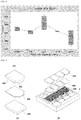
FIGS. 4 and5 are conceptual diagrams of a light-emitting package manufactured according to an embodiment of the present invention and a printed circuit board (PCB) to which the light-emitting package is applied. -
FIG. 6 is a conceptual diagram of a vehicle lighting device to which a light-emitting package manufactured according to an embodiment of the present invention is applied. - Exemplary embodiments of the present invention that can be easily implemented by one skilled in the art will now be described more fully with reference to the accompanying drawings in which the exemplary embodiments of the invention are shown. However, an embodiment described herein and components shown in the drawings are only an exemplary embodiment of the present invention, and it should be understood that various equivalents and modifications could be made thereto at the time of filing of the present application. Further, in the following detailed description of operating principles of exemplary embodiments of the present invention, a detailed description of known functions and configurations incorporated therein will be omitted so as not to unnecessarily obscure embodiments of the present invention. The following terms are defined in consideration of functions in the present invention, and the meanings of the respective terms should be interpreted based on contents of the entire present specification.
- As shown in
FIG. 1 , a light-emitting package 100 according to an embodiment of the present invention may have a structure in which a light-emittingunit 200, anadhesive member 300, and a photo-conversion substrate 400 are sequentially stacked. The light-emittingunit 200 may be any one selected from a light-emitting diode (LED), an organic LED (OLED), a laser diode (LD), a laser, and a vertical-cavity surface-emitting laser (VCSEL). Effects of high light extraction efficiency and thermal stability according to the present invention are more suitable for LEDs. - The
adhesive member 300 may be interposed and formed between the light-emittingunit 200 and the photo-conversion substrate 400. Theadhesive member 300 may includeinorganic nanoparticles 301 dispersed in a silicone-based resin. An ethyl-based, butyl-based, or methyl-based resin or a phenyl-based silicone-based resin may be used as the silicone-based resin. A metal silicone may maintain a high refractive index and thermal stability. - Inorganic nanoparticles, which are dispersed in a silicone-based resin, and particularly, a methyl silicone resin to maintain thermal stability and have a high refractive index, may be used as the
inorganic nanoparticles 301 capable of maintaining thermal stability and having a high refractive index. Test results according to an embodiment of the present invention revealed that TiO2 or ZrO2 inorganic nanoparticles and inorganic nanoparticles including TiO2 or ZrO2 maintained high thermal stability and exhibited excellent light extraction effects. - The
adhesive member 300 may be formed to have a high refractive index of nearly 1.6 by dispersing TiO2 or ZrO2inorganic nanoparticles 301 in the silicone-based resin. Due to the high refractive index, theadhesive member 300 may effectively improve light extraction without optical loss between the light-emittingunit 200 having a refractive index of about 2.4 and being disposed under theadhesive member 300 and the photo-conversion substrate 400 having a refractive index of about 1.6 and being stacked on theadhesive member 300. When theadhesive member 300 has a refractive index of about 2.0, which is intermediate between 1.6 and 2.4, it would be ideal for light extraction. However, when a resin adhesive member is used, it is practically impossible to achieve a refractive index as high as 2.0. This is because even a resin adhesive having a high refractive index, from among presently known resin adhesives, has a refractive index of about 1.4. In addition, even if a resin adhesive has a high refractive index, since the resin adhesive needs attendant thermal stability, a polymer resin that may simultaneously satisfy both a high refractive index and thermal stability may be a silicone-based resin, and particularly, a methyl silicone resin, which is an embodiment of the present invention. - However, since the methyl silicone resin also has a refractive index of about 1.41, there is a limit to improving light extraction efficiency only by using a methyl silicone itself. Thus, according to an embodiment of the present invention, when
inorganic nanoparticles 301 are used in a certain amount, a refractive index of theadhesive member 300 may be increased and thermal stability and a high refractive index may be obtained. To this end, theinorganic nanoparticles 301 included in theadhesive member 300 may include, for example, at least one material selected from the group consisting of titanium dioxide (TiO2) sol, strontium titanate (SrTiO3) sol, zinc sulfide (ZnS), selenium sulfide (ZnSe), potassium bromide (KBr), silver chloride (AgCl), magnesium oxide (MgO), cerium iodide (CeI), cerium bromide (CsBr), calcium carbonate (CaCO3), phosphorus tribromide (PBr3), trichlorobenzene (C6H3Cl3), naphthalene (C18H15Cl), triochroman-4-one, thionyl bromide (SOBr2), zinc oxide (ZnO2), cerium oxide (CeO2), indium tin oxide (ITO) sol, tantalum oxide (Ta2O5), titanium peroxide (Ti2O5), titanium suboxide (Ti2O3), zirconium oxide (ZrO2), bromine (Br2), carbon disulfide (CS2), ZrO2-TiO2-based sol, and a SiO2-Fe2O3-based compound. Particularly, theinorganic nanoparticles 301 included in theadhesive member 300 may include nanoscale TiO2 and nanoscale zirconium oxide, that is, zirconia (ZrO2). - TiO2 preferably has a particle size of 50 nm to 200 nm, and ZrO2 preferably has a particle size of 10 nm to 150 nm. When the particle sizes of TiO2 and ZrO2 were less than the above-mentioned ranges, the inorganic particles were not properly dispersed due to severe agglomeration of the inorganic particles. When the particle sizes of TiO2 and ZrO2 exceeded the above-mentioned ranges, refractive-index increasing effects were insufficient. Table 1 shows results obtained by testing light extraction (luminous flux) effects using TiO2 having a particle size of 100 nm. An adhesive member was prepared by dispersing TiO2 in a methyl silicone resin according to content of Table 1. Thereafter, a light-emitting package was manufactured by interposing the adhesive member between an LED light-emitting unit and a photo-conversion substrate including yttrium aluminum garnet (YAG) phosphor. Thus, the light-emitting package was tested.
[Table 1] TiO2 content No. Luminous flux [1m] Cx Cy CCT [K] 0 wt% 1 281.32 0.3039 0.2977 7466 2 286.35 0.3041 0.2957 7490 3 290.18 0.3091 0.3052 6962 4 291.75 0.308 0.3007 7104 Average 287.4 0.3063 0.2998 7256 0.05 wt% 1 290.62 0.3073 0.3048 7093 2 294.59 0.3089 0.3075 6946 3 290.32 0.3119 0.3115 6703 4 288.81 0.3099 0.3053 6906 Average 291.1 0.3095 0.3073 6912 0.1 wt% 1 281.71 0.31 0.3052 6900 2 276.14 0.3058 0.2987 7301 3 295.95 0.3076 0.3062 7052 4 289.96 0.313 0.3136 6613 Average 285.9 0.3091 0.3059 6967 0.3 wt% 1 289.04 0.3083 0.3064 7001 2 285.7 0.3099 0.3062 6894 3 279.67 0.3076 0.3039 7085 4 279.83 0.3074 0.3041 7097 Average 283.6 0.3083 0.3052 7019 - Referring to Table 1 and
FIG. 2 , it can be seen that when a TiO2 content was 0.05 wt%, a luminous flux was highest and increased 1.3% to 2.6% compared to other test conditions. Further, it can be seen that when the TiO2 content exceeded 0.05 w%, the luminous flux sharply dropped. These results show that the nanoscale TiO2 content percentage affects the luminous flux of the light-emitting package at a trace level. - Table 2 shows results obtained by testing luminous fluxes using ZrO2 having a particle size of 50 nm under the same experimental conditions as those of TiO2.
[Table 2] ZrO2 content No. Luminous flux [1m] Cx Cy CCT [K] 0 wt% 1 297.8 0.320 0.331 6107 2 291.9 0.319 0.329 6194 3 293.3 0.319 0.331 6149 4 295.2 0.321 0.333 6042 Average 294.6 0.320 0.331 6123 4.5 wt% 1 287.6 0.313 0.322 6552 2 292.2 0.319 0.329 6188 3 291.5 0.319 0.329 6178 4 293.0 0.318 0.328 6211 Average 291.1 0.317 0.327 6282 9 wt% 1 293.1 0.320 0.335 6090 2 296.1 0.323 0.340 5946 3 301.6 0.325 0.341 5829 4 313.7 0.325 0.332 5856 Average 301.1 0.323 0.337 5930 13.5wt% 1 291.4 0.316 0.320 6414 2 292.0 0.316 0.320 6392 3 291.6 0.316 0.320 6399 4 291.7 0.316 0.320 6398 Average 291.7 0.316 0.320 6401 18wt% 1 284.8 0.322 0.335 6015 2 291.4 0.322 0.330 6034 3 272.0 0.315 0.323 6422 4 293.3 0.319 0.328 6188 Average 285.4 0.319 0.329 6165 - Referring to Table 2 and
FIG. 3 , it can be seen that when a ZrO2 content was 9 wt%, a luminous flux was highest and increased 2.1% to 5.2% compared to other test conditions. Further, it can be seen that when the ZrO2 content was less than or exceeded 9 wt%, the luminous flux rapidly dropped. These results show that the nanoscale ZrO2 content affects the luminous flux of the light-emitting package. - Referring to color temperatures of Table 2, it can be seen that when the ZrO2 content was 9 wt%, the color temperature was 5930 K, which was the result closest to 5700 K which is a color temperature of natural light (sunlight). For light, being similar to a color temperature of natural light signifies being easier for the naked human eye to recognize and to reduce eye fatigue.
- It was determined that a rise in the luminous flux of the light-
emitting package 100 was a result of an increase in the refractive index of theadhesive member 300. Thus, a refractive index of the adhesive member alone was measured to be about 1.58 to 1.62. Thus, it can be inferred that the refractive index of the adhesive member was equal to or higher than a refractive index of a photo-conversion substrate including inorganic phosphor. - The photo-
conversion substrate 400 according to the embodiment of the present invention may include a fluorescent material. Although a substrate formed of various light-transmissive materials may be applied to the photo-conversion substrate 400, a ceramic substrate may be applied to the photo-conversion substrate 400 in an exemplary embodiment of the present invention. - The fluorescent material included in the photo-
conversion substrate 400 may include phosphorus (P) capable of converting excitation light of various light-emittingunits 200 into converted light through the medium of phosphor, and the phosphor. Specifically, the fluorescent material may include at least one of yellow phosphor, green phosphor, and red phosphor. The yellow phosphor emits light having a main wavelength in the range of 540 nm to 585 nm in response to blue light (430 nm to 480 nm), and the green phosphor emits light having a main wavelength in the range of 510 nm to 535 nm in response to blue light (430 nm to 480 nm). The red phosphor emits light having a main wavelength in the range of 600 nm to 650 nm in response to blue light (430 nm to 480 nm). The yellow phosphor may be silicate-based or YAG-based phosphor, the green phosphor may be silicate-based, nitride-based, or sulfide-based phosphor, and the red phosphor may be nitride-based or sulfide-based phosphor.FIG. 4A is a conceptual diagram of a light-emittingpackage 100 according to an embodiment of the present invention, andFIG. 4B is a conceptual diagram of the light-emittingpackage 100 before the light-emittingpackage 100 is mounted on a printed circuit board (PCB) P.FIG. 5 shows a state in which the light-emitting package is mounted on a PCB. - As can be seen from
FIG. 4A , the light-emittingpackage 100 may be configured such that anadhesive member 300 is disposed between a light-emittingunit 200 and a photo-conversion substrate 400.Groove units 401 serving as paths for wires configured to electrically connect the PCB P with the light-emittingunit 200 may be formed in the photo-conversion substrate 400 and theadhesive member 300. The light-emittingunit 200 may be any one selected from an LED, an OLED, an LD, a laser, and a VCSEL. Particularly, the light-emittingpackage 100 manufactured according to the present invention may achieve high thermal stability and light extraction efficiency when an LED light source is used. -
FIG. 6 is a conceptual diagram of a vehicle lighting device to which a light-emittingpackage 100 according to an embodiment of the present invention is applied. Light converted by a photo-conversion substrate of the light-emittingpackage 100 proceeds to areflector 500 and is emitted in an X direction. A reflective member (not shown) is disposed on a rear surface of the light-emittingpackage 100 so that converted light proceeding to the light-emittingpackage 100 may be partially reflected, return to thereflector 500, and be emitted. - Further, in the present invention, a light-emitting unit may be disposed on a PCB. A photo-conversion substrate may be disposed on the light-emitting unit. An adhesive member may be disposed between the light-emitting unit and the photo-conversion substrate. Although not shown in the present invention, a transparent substrate may be disposed between the light-emitting unit and the adhesive member. The light-emitting unit may be in contact with or spaced apart from the transparent substrate. The transparent substrate may be a metal oxide substrate, a sapphire substrate, or a plastic substrate. In the present invention, the light-emitting unit may be used interchangeably with a concept including a transparent substrate.
- A plurality of light-emitting units may be provided. The light-emitting unit may include a light source mounted on a substrate, and a plurality of light sources may be provided. The plurality of light sources may be disposed on a plurality of photo-conversion substrates or a single photo-conversion substrate. Further, the adhesive member disposed between the light-emitting unit and the photo-conversion substrate may be also disposed between the photo-conversion substrate and the photo-conversion substrate.
- The photo-conversion substrate may be in contact with the light-emitting unit or spaced apart from the light-emitting unit.
- While specific embodiments have been described in the above detailed description of the present invention, various changes in form and details may be made to the embodiments without departing from the spirit and scope of the present invention. The technical spirit of the present invention should not be limited to the above-described embodiments of the present invention but should be defined by the following claims and the equivalents thereof.
-
100: light-emitting package 200: light-emitting unit 300: adhesive member 301: inorganic nanoparticles 400: photo-conversion substrate 500: reflector
Claims (20)
- A light-emitting package comprising:a light-emitting unit;a photo-conversion substrate disposed on one surface of the light-emitting unit; andan adhesive member disposed between the light-emitting unit and the photo-conversion substrate, the adhesive member comprising inorganic nanoparticles dispersed in a silicone-based resin.
- The light-emitting package of claim 1, wherein a refractive index of the adhesive member is higher than a refractive index of the photo-conversion substrate.
- The light-emitting package of claim 2, wherein a refractive index of the adhesive member ranges from 1.58 to 1.62.
- The light-emitting package of claim 1, wherein a difference in refractive index between the adhesive member and the photo-conversion substrate is 0.8 or less.
- The light-emitting package of claim 1, wherein the inorganic nanoparticles comprise at least one material selected from ZrO2-TiO2-based sol and a SiO2- Fe2O3-based compound or at least one material selected from titanium dioxide (TiO2) and zirconia (or zirconium oxide) (ZrO2).
- The light-emitting package of claim 1, wherein the silicone-based resin is a methyl silicone resin.
- The light-emitting package of claim 1, wherein the silicone-based resin is a phenyl silicone resin.
- The light-emitting package of claim 5, wherein the inorganic nanoparticles are TiO2.
- The light-emitting package of claim 8, wherein TiO2 has a particle size of 50 nm to 200 nm and is contained at a content of 0.04 to 0.06% by weight in the adhesive member.
- The light-emitting package of claim 9, wherein the adhesive member has a luminous flux of 290 lm or higher.
- The light-emitting package of claim 5, wherein the inorganic nanoparticles are ZrO2.
- The light-emitting package of claim 11, wherein ZrO2 has a particle size of 10 nm to 150 nm and is contained at a content of 7 to 11.5% by weight in the adhesive member.
- The light-emitting package of claim 12, wherein the adhesive member has a luminous flux of 300 lm or higher.
- A vehicle lighting device comprising:a light-emitting package comprising a light-emitting unit, a photo-conversion substrate disposed on one surface of the light-emitting unit, and an adhesive member disposed between the light-emitting unit and the photo-conversion substrate, the adhesive member comprising inorganic nanoparticles dispersed in a silicone-based resin; anda reflector configured to reflect converted light emitted by the light-emitting package.
- The vehicle lighting device of claim 14, wherein a refractive index of the adhesive member is higher than a refractive index of the photo-conversion substrate.
- The vehicle lighting device of claim 15, wherein a difference in refractive index between the adhesive member and the photo-conversion substrate is 0.8 or less.
- The vehicle lighting device of claim 14, further comprising a transparent substrate disposed between the light-emitting unit and the adhesive member.
- The vehicle lighting device of claim 14, further comprising a support substrate disposed to be in contact with one surface of the photo-conversion substrate, the support substrate having a groove in which the photo-conversion substrate is disposed, the support substrate being in contact with the reflector.
- A vehicle lighting device comprising:a light-emitting unit;a photo-conversion substrate disposed on one surface of the light-emitting unit;an adhesive member disposed between the light-emitting unit and the photo-conversion substrate, the adhesive member comprising inorganic nanoparticles dispersed in a silicone-based resin;a transparent substrate disposed between the light-emitting unit and the adhesive member, wherein the light-emitting unit is spaced apart from the transparent substrate; anda support substrate comprising a groove in which the photo-conversion substrate is disposed, the support substrate being in contact with a reflector.
- The vehicle lighting device of claim 19, wherein a difference in refractive index between the adhesive member and the photo-conversion substrate is 0.8 or less.
Applications Claiming Priority (2)
| Application Number | Priority Date | Filing Date | Title |
|---|---|---|---|
| KR1020150155764A KR102499548B1 (en) | 2015-11-06 | 2015-11-06 | light emitting Package and automobile lamp using the same |
| PCT/KR2016/012683 WO2017078474A1 (en) | 2015-11-06 | 2016-11-04 | Light emitting package and vehicle lighting device comprising same |
Publications (3)
| Publication Number | Publication Date |
|---|---|
| EP3373346A1 true EP3373346A1 (en) | 2018-09-12 |
| EP3373346A4 EP3373346A4 (en) | 2019-04-24 |
| EP3373346B1 EP3373346B1 (en) | 2020-10-28 |
Family
ID=58662401
Family Applications (1)
| Application Number | Title | Priority Date | Filing Date |
|---|---|---|---|
| EP16862489.8A Active EP3373346B1 (en) | 2015-11-06 | 2016-11-04 | Light emitting package and vehicle lighting device comprising same |
Country Status (6)
| Country | Link |
|---|---|
| US (1) | US10527231B2 (en) |
| EP (1) | EP3373346B1 (en) |
| JP (1) | JP2018534780A (en) |
| KR (1) | KR102499548B1 (en) |
| CN (1) | CN108323216A (en) |
| WO (1) | WO2017078474A1 (en) |
Families Citing this family (2)
| Publication number | Priority date | Publication date | Assignee | Title |
|---|---|---|---|---|
| US10128419B1 (en) * | 2017-08-03 | 2018-11-13 | Lumileds Llc | Method of manufacturing a light emitting device |
| CN112456552A (en) * | 2020-12-14 | 2021-03-09 | 新沂市锡沂高新材料产业技术研究院有限公司 | Pretreatment method and application of nano zirconia |
Family Cites Families (25)
| Publication number | Priority date | Publication date | Assignee | Title |
|---|---|---|---|---|
| US7160972B2 (en) * | 2003-02-19 | 2007-01-09 | Nusil Technology Llc | Optically clear high temperature resistant silicone polymers of high refractive index |
| US20070001182A1 (en) * | 2005-06-30 | 2007-01-04 | 3M Innovative Properties Company | Structured phosphor tape article |
| WO2007018039A1 (en) * | 2005-08-05 | 2007-02-15 | Matsushita Electric Industrial Co., Ltd. | Semiconductor light-emitting device |
| JP2009538955A (en) | 2006-05-29 | 2009-11-12 | コーニンクレッカ フィリップス エレクトロニクス エヌ ヴィ | Inorganic phosphors for light-emitting diodes |
| US7521862B2 (en) | 2006-11-20 | 2009-04-21 | Philips Lumileds Lighting Co., Llc | Light emitting device including luminescent ceramic and light-scattering material |
| JP5012230B2 (en) * | 2007-06-07 | 2012-08-29 | 住友大阪セメント株式会社 | Zirconia-containing silicone resin composition |
| JP4796031B2 (en) * | 2007-09-28 | 2011-10-19 | パナソニック株式会社 | Vehicle headlight light source and vehicle headlight |
| JPWO2010044239A1 (en) * | 2008-10-17 | 2012-03-15 | 株式会社小糸製作所 | Light emitting module, method for manufacturing light emitting module, and lamp unit |
| JP5434045B2 (en) * | 2008-10-21 | 2014-03-05 | Jsr株式会社 | Photoelectric conversion element and composition for coating optical semiconductor element |
| JP5552243B2 (en) * | 2009-02-26 | 2014-07-16 | 日東電工株式会社 | Metal oxide fine particles |
| EP2464685A1 (en) * | 2009-08-12 | 2012-06-20 | Koninklijke Philips Electronics N.V. | Optical composition |
| JP5463901B2 (en) * | 2009-12-24 | 2014-04-09 | 日亜化学工業株式会社 | Light emitting device |
| US8771577B2 (en) * | 2010-02-16 | 2014-07-08 | Koninklijke Philips N.V. | Light emitting device with molded wavelength converting layer |
| JP4875185B2 (en) * | 2010-06-07 | 2012-02-15 | 株式会社東芝 | Optical semiconductor device |
| KR101719655B1 (en) | 2010-09-29 | 2017-03-24 | 서울반도체 주식회사 | Phosphor sheet, light-emitting device having the phosphor sheet and method of manufacturing the same |
| WO2012050199A1 (en) * | 2010-10-15 | 2012-04-19 | 三菱化学株式会社 | White light emitting device and lighting device |
| EP2641277A4 (en) | 2010-11-18 | 2016-06-15 | 3M Innovative Properties Co | LIGHT EMITTING DIODE COMPONENT COMPRISING A POLYSILAZANE BONDING LAYER |
| KR101539486B1 (en) * | 2011-01-06 | 2015-07-24 | 주식회사 엘지화학 | Curable composition |
| JP5707618B2 (en) * | 2011-06-30 | 2015-04-30 | シャープ株式会社 | Light emitting device |
| JP6125776B2 (en) * | 2012-09-03 | 2017-05-10 | シャープ株式会社 | Floodlight device |
| JP6040019B2 (en) * | 2012-12-10 | 2016-12-07 | スタンレー電気株式会社 | Semiconductor light emitting device |
| TWI531094B (en) * | 2013-05-17 | 2016-04-21 | Daxin Materials Corp | And a light-emitting device for a light-emitting device |
| JP5935067B2 (en) * | 2013-10-10 | 2016-06-15 | パナソニックIpマネジメント株式会社 | Wavelength conversion plate and lighting device using the same |
| JP2015149172A (en) * | 2014-02-06 | 2015-08-20 | 東レ株式会社 | Composite sheet, led package prepared using the same, and method of producing the same |
| KR102231580B1 (en) * | 2014-02-14 | 2021-03-24 | 엘지이노텍 주식회사 | Light conversion element, Lamp package and automobile lamp using the same |
-
2015
- 2015-11-06 KR KR1020150155764A patent/KR102499548B1/en active Active
-
2016
- 2016-11-04 US US15/773,909 patent/US10527231B2/en active Active
- 2016-11-04 EP EP16862489.8A patent/EP3373346B1/en active Active
- 2016-11-04 JP JP2018522679A patent/JP2018534780A/en active Pending
- 2016-11-04 WO PCT/KR2016/012683 patent/WO2017078474A1/en not_active Ceased
- 2016-11-04 CN CN201680064954.6A patent/CN108323216A/en active Pending
Also Published As
| Publication number | Publication date |
|---|---|
| EP3373346B1 (en) | 2020-10-28 |
| EP3373346A4 (en) | 2019-04-24 |
| US10527231B2 (en) | 2020-01-07 |
| JP2018534780A (en) | 2018-11-22 |
| WO2017078474A1 (en) | 2017-05-11 |
| US20180335182A1 (en) | 2018-11-22 |
| KR102499548B1 (en) | 2023-03-03 |
| KR20170053357A (en) | 2017-05-16 |
| CN108323216A (en) | 2018-07-24 |
Similar Documents
| Publication | Publication Date | Title |
|---|---|---|
| KR101798216B1 (en) | Illumination device with remote luminescent material | |
| KR101363116B1 (en) | Planar light-emitting module | |
| KR102737501B1 (en) | Led device and led lamp using the same | |
| JP5654378B2 (en) | Light emitting device | |
| CN106030835A (en) | Wavelength conversion member and light emitting device using same | |
| KR20140113850A (en) | Semiconductor light emitting device package | |
| CN101621054A (en) | LED light source device | |
| US20180358520A1 (en) | Light emitting device package and lighting system comprising same | |
| TW201806189A (en) | Wafer-level package light-emitting device with moisture barrier structure | |
| KR102648863B1 (en) | Light emitting diode package | |
| KR102550415B1 (en) | Led device and led lamp using the same | |
| US9989197B2 (en) | Optical device and light source module including the same | |
| US10527231B2 (en) | Light emitting package and vehicle lighting device comprising same | |
| EP3396230B1 (en) | Phosphor plate package, light-emitting package, and vehicle head lamp comprising same | |
| US20170040506A1 (en) | Light-emitting apparatus and illumination apparatus | |
| JP2008244468A (en) | Light emitting device | |
| JP2020061521A (en) | Light-emitting device | |
| KR102397909B1 (en) | Board and light source module having the same | |
| JP6203089B2 (en) | Semiconductor light emitting device | |
| JP6803539B2 (en) | Light emitting device and lighting device | |
| TWI362746B (en) | Light emitting diode lighting device | |
| KR102378761B1 (en) | Unified light emitting Package and automobile lamp using the same | |
| CN110391217B (en) | Light-emitting devices, lighting devices and silicone resins | |
| JP2017171706A (en) | Red phosphor and light emitting module | |
| KR102541459B1 (en) | Glass composition for phosphor plate and phosphor plate using the same |
Legal Events
| Date | Code | Title | Description |
|---|---|---|---|
| STAA | Information on the status of an ep patent application or granted ep patent |
Free format text: STATUS: THE INTERNATIONAL PUBLICATION HAS BEEN MADE |
|
| PUAI | Public reference made under article 153(3) epc to a published international application that has entered the european phase |
Free format text: ORIGINAL CODE: 0009012 |
|
| STAA | Information on the status of an ep patent application or granted ep patent |
Free format text: STATUS: REQUEST FOR EXAMINATION WAS MADE |
|
| 17P | Request for examination filed |
Effective date: 20180601 |
|
| AK | Designated contracting states |
Kind code of ref document: A1 Designated state(s): AL AT BE BG CH CY CZ DE DK EE ES FI FR GB GR HR HU IE IS IT LI LT LU LV MC MK MT NL NO PL PT RO RS SE SI SK SM TR |
|
| AX | Request for extension of the european patent |
Extension state: BA ME |
|
| RIC1 | Information provided on ipc code assigned before grant |
Ipc: F21K 9/20 20160101ALI20181210BHEP Ipc: H01L 33/50 20100101ALI20181210BHEP Ipc: H01L 33/60 20100101ALI20181210BHEP Ipc: F21S 43/14 20180101ALI20181210BHEP Ipc: H01L 33/56 20100101ALI20181210BHEP Ipc: H01L 33/48 20100101AFI20181210BHEP Ipc: F21Y 101/00 20160101ALI20181210BHEP |
|
| DAV | Request for validation of the european patent (deleted) | ||
| DAX | Request for extension of the european patent (deleted) | ||
| A4 | Supplementary search report drawn up and despatched |
Effective date: 20190327 |
|
| RIC1 | Information provided on ipc code assigned before grant |
Ipc: F21S 43/14 20180101ALI20190321BHEP Ipc: F21K 9/20 20160101ALI20190321BHEP Ipc: F21Y 101/00 20160101ALI20190321BHEP Ipc: H01L 33/60 20100101ALI20190321BHEP Ipc: H01L 33/50 20100101ALI20190321BHEP Ipc: H01L 33/56 20100101ALI20190321BHEP Ipc: H01L 33/48 20100101AFI20190321BHEP |
|
| GRAP | Despatch of communication of intention to grant a patent |
Free format text: ORIGINAL CODE: EPIDOSNIGR1 |
|
| STAA | Information on the status of an ep patent application or granted ep patent |
Free format text: STATUS: GRANT OF PATENT IS INTENDED |
|
| INTG | Intention to grant announced |
Effective date: 20200526 |
|
| GRAS | Grant fee paid |
Free format text: ORIGINAL CODE: EPIDOSNIGR3 |
|
| GRAA | (expected) grant |
Free format text: ORIGINAL CODE: 0009210 |
|
| STAA | Information on the status of an ep patent application or granted ep patent |
Free format text: STATUS: THE PATENT HAS BEEN GRANTED |
|
| AK | Designated contracting states |
Kind code of ref document: B1 Designated state(s): AL AT BE BG CH CY CZ DE DK EE ES FI FR GB GR HR HU IE IS IT LI LT LU LV MC MK MT NL NO PL PT RO RS SE SI SK SM TR |
|
| REG | Reference to a national code |
Ref country code: GB Ref legal event code: FG4D |
|
| REG | Reference to a national code |
Ref country code: CH Ref legal event code: EP |
|
| REG | Reference to a national code |
Ref country code: AT Ref legal event code: REF Ref document number: 1329108 Country of ref document: AT Kind code of ref document: T Effective date: 20201115 |
|
| REG | Reference to a national code |
Ref country code: DE Ref legal event code: R096 Ref document number: 602016046889 Country of ref document: DE |
|
| REG | Reference to a national code |
Ref country code: IE Ref legal event code: FG4D |
|
| REG | Reference to a national code |
Ref country code: AT Ref legal event code: MK05 Ref document number: 1329108 Country of ref document: AT Kind code of ref document: T Effective date: 20201028 |
|
| REG | Reference to a national code |
Ref country code: NL Ref legal event code: MP Effective date: 20201028 |
|
| PG25 | Lapsed in a contracting state [announced via postgrant information from national office to epo] |
Ref country code: GR Free format text: LAPSE BECAUSE OF FAILURE TO SUBMIT A TRANSLATION OF THE DESCRIPTION OR TO PAY THE FEE WITHIN THE PRESCRIBED TIME-LIMIT Effective date: 20210129 Ref country code: FI Free format text: LAPSE BECAUSE OF FAILURE TO SUBMIT A TRANSLATION OF THE DESCRIPTION OR TO PAY THE FEE WITHIN THE PRESCRIBED TIME-LIMIT Effective date: 20201028 Ref country code: NO Free format text: LAPSE BECAUSE OF FAILURE TO SUBMIT A TRANSLATION OF THE DESCRIPTION OR TO PAY THE FEE WITHIN THE PRESCRIBED TIME-LIMIT Effective date: 20210128 Ref country code: PT Free format text: LAPSE BECAUSE OF FAILURE TO SUBMIT A TRANSLATION OF THE DESCRIPTION OR TO PAY THE FEE WITHIN THE PRESCRIBED TIME-LIMIT Effective date: 20210301 Ref country code: RS Free format text: LAPSE BECAUSE OF FAILURE TO SUBMIT A TRANSLATION OF THE DESCRIPTION OR TO PAY THE FEE WITHIN THE PRESCRIBED TIME-LIMIT Effective date: 20201028 |
|
| REG | Reference to a national code |
Ref country code: LT Ref legal event code: MG4D |
|
| PG25 | Lapsed in a contracting state [announced via postgrant information from national office to epo] |
Ref country code: ES Free format text: LAPSE BECAUSE OF FAILURE TO SUBMIT A TRANSLATION OF THE DESCRIPTION OR TO PAY THE FEE WITHIN THE PRESCRIBED TIME-LIMIT Effective date: 20201028 Ref country code: AT Free format text: LAPSE BECAUSE OF FAILURE TO SUBMIT A TRANSLATION OF THE DESCRIPTION OR TO PAY THE FEE WITHIN THE PRESCRIBED TIME-LIMIT Effective date: 20201028 Ref country code: IS Free format text: LAPSE BECAUSE OF FAILURE TO SUBMIT A TRANSLATION OF THE DESCRIPTION OR TO PAY THE FEE WITHIN THE PRESCRIBED TIME-LIMIT Effective date: 20210228 Ref country code: PL Free format text: LAPSE BECAUSE OF FAILURE TO SUBMIT A TRANSLATION OF THE DESCRIPTION OR TO PAY THE FEE WITHIN THE PRESCRIBED TIME-LIMIT Effective date: 20201028 Ref country code: LV Free format text: LAPSE BECAUSE OF FAILURE TO SUBMIT A TRANSLATION OF THE DESCRIPTION OR TO PAY THE FEE WITHIN THE PRESCRIBED TIME-LIMIT Effective date: 20201028 Ref country code: BG Free format text: LAPSE BECAUSE OF FAILURE TO SUBMIT A TRANSLATION OF THE DESCRIPTION OR TO PAY THE FEE WITHIN THE PRESCRIBED TIME-LIMIT Effective date: 20210128 Ref country code: SE Free format text: LAPSE BECAUSE OF FAILURE TO SUBMIT A TRANSLATION OF THE DESCRIPTION OR TO PAY THE FEE WITHIN THE PRESCRIBED TIME-LIMIT Effective date: 20201028 |
|
| PG25 | Lapsed in a contracting state [announced via postgrant information from national office to epo] |
Ref country code: HR Free format text: LAPSE BECAUSE OF FAILURE TO SUBMIT A TRANSLATION OF THE DESCRIPTION OR TO PAY THE FEE WITHIN THE PRESCRIBED TIME-LIMIT Effective date: 20201028 Ref country code: NL Free format text: LAPSE BECAUSE OF FAILURE TO SUBMIT A TRANSLATION OF THE DESCRIPTION OR TO PAY THE FEE WITHIN THE PRESCRIBED TIME-LIMIT Effective date: 20201028 |
|
| REG | Reference to a national code |
Ref country code: CH Ref legal event code: PL |
|
| REG | Reference to a national code |
Ref country code: DE Ref legal event code: R097 Ref document number: 602016046889 Country of ref document: DE |
|
| PG25 | Lapsed in a contracting state [announced via postgrant information from national office to epo] |
Ref country code: MC Free format text: LAPSE BECAUSE OF FAILURE TO SUBMIT A TRANSLATION OF THE DESCRIPTION OR TO PAY THE FEE WITHIN THE PRESCRIBED TIME-LIMIT Effective date: 20201028 Ref country code: LU Free format text: LAPSE BECAUSE OF NON-PAYMENT OF DUE FEES Effective date: 20201104 Ref country code: LT Free format text: LAPSE BECAUSE OF FAILURE TO SUBMIT A TRANSLATION OF THE DESCRIPTION OR TO PAY THE FEE WITHIN THE PRESCRIBED TIME-LIMIT Effective date: 20201028 Ref country code: SM Free format text: LAPSE BECAUSE OF FAILURE TO SUBMIT A TRANSLATION OF THE DESCRIPTION OR TO PAY THE FEE WITHIN THE PRESCRIBED TIME-LIMIT Effective date: 20201028 Ref country code: CZ Free format text: LAPSE BECAUSE OF FAILURE TO SUBMIT A TRANSLATION OF THE DESCRIPTION OR TO PAY THE FEE WITHIN THE PRESCRIBED TIME-LIMIT Effective date: 20201028 Ref country code: EE Free format text: LAPSE BECAUSE OF FAILURE TO SUBMIT A TRANSLATION OF THE DESCRIPTION OR TO PAY THE FEE WITHIN THE PRESCRIBED TIME-LIMIT Effective date: 20201028 Ref country code: SK Free format text: LAPSE BECAUSE OF FAILURE TO SUBMIT A TRANSLATION OF THE DESCRIPTION OR TO PAY THE FEE WITHIN THE PRESCRIBED TIME-LIMIT Effective date: 20201028 Ref country code: RO Free format text: LAPSE BECAUSE OF FAILURE TO SUBMIT A TRANSLATION OF THE DESCRIPTION OR TO PAY THE FEE WITHIN THE PRESCRIBED TIME-LIMIT Effective date: 20201028 |
|
| REG | Reference to a national code |
Ref country code: BE Ref legal event code: MM Effective date: 20201130 |
|
| PG25 | Lapsed in a contracting state [announced via postgrant information from national office to epo] |
Ref country code: CH Free format text: LAPSE BECAUSE OF NON-PAYMENT OF DUE FEES Effective date: 20201130 Ref country code: DK Free format text: LAPSE BECAUSE OF FAILURE TO SUBMIT A TRANSLATION OF THE DESCRIPTION OR TO PAY THE FEE WITHIN THE PRESCRIBED TIME-LIMIT Effective date: 20201028 Ref country code: LI Free format text: LAPSE BECAUSE OF NON-PAYMENT OF DUE FEES Effective date: 20201130 |
|
| PLBE | No opposition filed within time limit |
Free format text: ORIGINAL CODE: 0009261 |
|
| STAA | Information on the status of an ep patent application or granted ep patent |
Free format text: STATUS: NO OPPOSITION FILED WITHIN TIME LIMIT |
|
| 26N | No opposition filed |
Effective date: 20210729 |
|
| PG25 | Lapsed in a contracting state [announced via postgrant information from national office to epo] |
Ref country code: IT Free format text: LAPSE BECAUSE OF FAILURE TO SUBMIT A TRANSLATION OF THE DESCRIPTION OR TO PAY THE FEE WITHIN THE PRESCRIBED TIME-LIMIT Effective date: 20201028 Ref country code: FR Free format text: LAPSE BECAUSE OF NON-PAYMENT OF DUE FEES Effective date: 20201228 Ref country code: AL Free format text: LAPSE BECAUSE OF FAILURE TO SUBMIT A TRANSLATION OF THE DESCRIPTION OR TO PAY THE FEE WITHIN THE PRESCRIBED TIME-LIMIT Effective date: 20201028 Ref country code: IE Free format text: LAPSE BECAUSE OF NON-PAYMENT OF DUE FEES Effective date: 20201104 |
|
| PG25 | Lapsed in a contracting state [announced via postgrant information from national office to epo] |
Ref country code: SI Free format text: LAPSE BECAUSE OF FAILURE TO SUBMIT A TRANSLATION OF THE DESCRIPTION OR TO PAY THE FEE WITHIN THE PRESCRIBED TIME-LIMIT Effective date: 20201028 |
|
| PG25 | Lapsed in a contracting state [announced via postgrant information from national office to epo] |
Ref country code: IS Free format text: LAPSE BECAUSE OF FAILURE TO SUBMIT A TRANSLATION OF THE DESCRIPTION OR TO PAY THE FEE WITHIN THE PRESCRIBED TIME-LIMIT Effective date: 20210228 Ref country code: TR Free format text: LAPSE BECAUSE OF FAILURE TO SUBMIT A TRANSLATION OF THE DESCRIPTION OR TO PAY THE FEE WITHIN THE PRESCRIBED TIME-LIMIT Effective date: 20201028 Ref country code: MT Free format text: LAPSE BECAUSE OF FAILURE TO SUBMIT A TRANSLATION OF THE DESCRIPTION OR TO PAY THE FEE WITHIN THE PRESCRIBED TIME-LIMIT Effective date: 20201028 Ref country code: CY Free format text: LAPSE BECAUSE OF FAILURE TO SUBMIT A TRANSLATION OF THE DESCRIPTION OR TO PAY THE FEE WITHIN THE PRESCRIBED TIME-LIMIT Effective date: 20201028 |
|
| PG25 | Lapsed in a contracting state [announced via postgrant information from national office to epo] |
Ref country code: MK Free format text: LAPSE BECAUSE OF FAILURE TO SUBMIT A TRANSLATION OF THE DESCRIPTION OR TO PAY THE FEE WITHIN THE PRESCRIBED TIME-LIMIT Effective date: 20201028 |
|
| PG25 | Lapsed in a contracting state [announced via postgrant information from national office to epo] |
Ref country code: BE Free format text: LAPSE BECAUSE OF NON-PAYMENT OF DUE FEES Effective date: 20201130 |
|
| PGFP | Annual fee paid to national office [announced via postgrant information from national office to epo] |
Ref country code: GB Payment date: 20221020 Year of fee payment: 7 Ref country code: DE Payment date: 20221020 Year of fee payment: 7 |
|
| REG | Reference to a national code |
Ref country code: DE Ref legal event code: R119 Ref document number: 602016046889 Country of ref document: DE |
|
| GBPC | Gb: european patent ceased through non-payment of renewal fee |
Effective date: 20231104 |
|
| PG25 | Lapsed in a contracting state [announced via postgrant information from national office to epo] |
Ref country code: DE Free format text: LAPSE BECAUSE OF NON-PAYMENT OF DUE FEES Effective date: 20240601 |
|
| PG25 | Lapsed in a contracting state [announced via postgrant information from national office to epo] |
Ref country code: GB Free format text: LAPSE BECAUSE OF NON-PAYMENT OF DUE FEES Effective date: 20231104 |
|
| PG25 | Lapsed in a contracting state [announced via postgrant information from national office to epo] |
Ref country code: GB Free format text: LAPSE BECAUSE OF NON-PAYMENT OF DUE FEES Effective date: 20231104 Ref country code: DE Free format text: LAPSE BECAUSE OF NON-PAYMENT OF DUE FEES Effective date: 20240601 |