EP3370377A1 - Paketweiterleitung - Google Patents
Paketweiterleitung Download PDFInfo
- Publication number
- EP3370377A1 EP3370377A1 EP16859102.2A EP16859102A EP3370377A1 EP 3370377 A1 EP3370377 A1 EP 3370377A1 EP 16859102 A EP16859102 A EP 16859102A EP 3370377 A1 EP3370377 A1 EP 3370377A1
- Authority
- EP
- European Patent Office
- Prior art keywords
- board
- pci
- packet
- data packet
- interface board
- Prior art date
- Legal status (The legal status is an assumption and is not a legal conclusion. Google has not performed a legal analysis and makes no representation as to the accuracy of the status listed.)
- Granted
Links
Images






Classifications
-
- H—ELECTRICITY
- H04—ELECTRIC COMMUNICATION TECHNIQUE
- H04L—TRANSMISSION OF DIGITAL INFORMATION, e.g. TELEGRAPHIC COMMUNICATION
- H04L49/00—Packet switching elements
- H04L49/40—Constructional details, e.g. power supply, mechanical construction or backplane
-
- G—PHYSICS
- G06—COMPUTING OR CALCULATING; COUNTING
- G06F—ELECTRIC DIGITAL DATA PROCESSING
- G06F13/00—Interconnection of, or transfer of information or other signals between, memories, input/output devices or central processing units
- G06F13/38—Information transfer, e.g. on bus
- G06F13/40—Bus structure
- G06F13/4004—Coupling between buses
- G06F13/4027—Coupling between buses using bus bridges
-
- G—PHYSICS
- G06—COMPUTING OR CALCULATING; COUNTING
- G06F—ELECTRIC DIGITAL DATA PROCESSING
- G06F13/00—Interconnection of, or transfer of information or other signals between, memories, input/output devices or central processing units
- G06F13/38—Information transfer, e.g. on bus
- G06F13/42—Bus transfer protocol, e.g. handshake; Synchronisation
- G06F13/4282—Bus transfer protocol, e.g. handshake; Synchronisation on a serial bus, e.g. I2C bus, SPI bus
-
- H—ELECTRICITY
- H04—ELECTRIC COMMUNICATION TECHNIQUE
- H04L—TRANSMISSION OF DIGITAL INFORMATION, e.g. TELEGRAPHIC COMMUNICATION
- H04L45/00—Routing or path finding of packets in data switching networks
- H04L45/74—Address processing for routing
-
- H—ELECTRICITY
- H04—ELECTRIC COMMUNICATION TECHNIQUE
- H04L—TRANSMISSION OF DIGITAL INFORMATION, e.g. TELEGRAPHIC COMMUNICATION
- H04L49/00—Packet switching elements
- H04L49/35—Switches specially adapted for specific applications
- H04L49/351—Switches specially adapted for specific applications for local area network [LAN], e.g. Ethernet switches
-
- G—PHYSICS
- G06—COMPUTING OR CALCULATING; COUNTING
- G06F—ELECTRIC DIGITAL DATA PROCESSING
- G06F2213/00—Indexing scheme relating to interconnection of, or transfer of information or other signals between, memories, input/output devices or central processing units
- G06F2213/0026—PCI express
-
- H—ELECTRICITY
- H04—ELECTRIC COMMUNICATION TECHNIQUE
- H04L—TRANSMISSION OF DIGITAL INFORMATION, e.g. TELEGRAPHIC COMMUNICATION
- H04L49/00—Packet switching elements
- H04L49/70—Virtual switches
Definitions
- a network device may include a forwarding board and at least two interface boards.
- the forwarding board is one board, which takes charge of forwarding and processing network packets.
- the interface board possesses an out interface of a physical network, which is in charge of transmitting and receiving network packets.
- a forwarding board may be connected with each interface board, by using a Peripheral Component Interconnect Express (PCI-E) bus.
- PCI-E Peripheral Component Interconnect Express
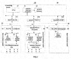
- a network device 10 may include a forwarding board 20, a first interface board 30 and a second interface board 40.
- the forwarding board 20 may include a CPU 21, a system memory 22, a system memory controller 23, a first PCI-E root complex (RC) 241 and a second PCI-E RC 242.
- the CPU 21, the system memory controller 23, the first PCI-E RC 241 and the second PCI-E RC 242 are connected with each other.
- the system memory 22 is connected with the system memory controller 23.
- the CPU 21, the system memory controller 23, the first PCI-E RC 241 and the second PCI-E RC 242 of the forwarding board may be integrated into a system-on-a-chip (SOC) CPU.
- the system memory controller 23 of the forwarding board may be integrated into the CPU 21.
- the first PCI-E RC 241 and the second PCI-E RC 242 of the forwarding board may be integrated into a platform controller hub (PCH) independent of the CPU 21.
- PCH platform controller hub
- first PCI-E RC 241 and the second PCI-E RC 242 in FIG.1 are independent of each other, which does not mean that the first PCI-E RC 241 and the second PCI-E RC 242 are two independent entities definitely. That is, the first PCI-E RC 241 and second PCI-E RC 242 in FIG.1 may be two equivalent PCI-E RCs, which are formed logically, by connecting an entity possessing functions of PCI-E RC to a PCI-E Switch externally.
- first PCI-E RC 241 and the second PCI-E RC 242 are two independent entities, either of the first PCI-E RC 241 and the second PCI-E RC 242 may be connected with the PCI-E switch externally.
- the first interface board 30 may include a first Ethernet switch chip 31, a first logical device 32, a first board memory 33, and a first PCI-E Endpoint 34 connecting with the first PCI-E RC 241 via a first PCI-E bus 11.
- the first Ethernet switch chip 31 and the first logical device 32 may be connected with each other (e.g., via an Ethernet bus).
- the first logical device 32, the first board memory 33 and the first PCI-E Endpoint 34 may be connected with each other.
- the second interface board 40 may include a second Ethernet switch chip 41, a second logical device 42, a second board memory 43, and a second PCI-E Enpoint 44 connecting with the second PCI-E RC 242 via a second PCI-E bus 12.
- the second Ethernet switch chip 41 and the second logical device 42 may be connected with each other (e.g., via the Ethernet bus).
- the second logical device 42, the second board memory 43 and the second PCI-E Endpoint 44 may be connected with each other.
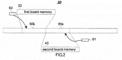
- a first board memory 33 and a second board memory 43 both map to PCI-E memory space 60 of the network device 10.
- an address range 60b in the PCI-E memory space 60 mapped by the first board memory 33 may be different from an address range 60a, which is also in the PCI-E memory space 60 mapped by the second board memory 43.
- the first PCI-E RC 241, the second PCI-E RC 242, the first PCI-E Endpoint 34 and the second PCI-E Endpoint 44, the first board memory 33 and the second board memory 43 are not transparent.
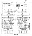
- the first logical device 32 in the first interface board 30 may determine the destination board of the Ethernet data packet 51.
- the Ethernet data packet 51 may be received from an exterior of the network device 10, by using the first Ethernet switch chip 31.
- the first logical device 32 may determine the destination board of the Ethernet data packet 51, based on a maintained a mapping table between an Ethernet media access control (MAC) address and a board identity (ID).
- MAC media access control
- ID board identity
- the Ethernet data packet 51 may be forwarded to the system memory 22 of the forwarding board 20 in PCI-E format, and then be read by the CPU 21 from the system memory 22 to be processed.
- the first logical device 32 may encapsulate the Ethernet data packet 51 into a PCI-E packet 61 (a PCI-E write packet in the application may be referred to as "the PCI-E packet" for short), which takes the PCI-E memory space address (that is, address within the address range 60a in FIG.2 ) of the second board memory 43 as the destination address, such that the first PCI-E Endpoint 34 may forward the PCI-E packet 61 to the forwarding board 20, and enable the forwarding board 20 to forward the PCI-E packet 61 to the second board memory 43 of the second interface board 40, which is taken as the destination board, by using the destination address of the PCI-E packet 61.
- the PCI-E packet takes the PCI-E memory space address (that is, address within the address range 60a in FIG.2 ) of the second board memory 43 as the destination address, such that the first PCI-E Endpoint 34 may forward the PCI-E packet 61 to the forwarding board 20, and enable the forwarding board 20 to forward the
- the first PCI-E Endpoint 34 may transmit the PCI-E packet 61 to the first PCI-E RC 241. And then, the first PCI-E RC 241 may forward the PCI-E packet 61 to the second PCI-E RC 242, based on the destination address of the PCI-E packet 61.
- the PCI-E packet 61 encapsulated with the Ethernet data packet 51 may be forwarded to the second PCI-E Endpoint 44 by the second PCI-E RC 242, and may be written into the second board memory 43 by the second PCI-E Endpoint 44.
- the second logical device 42 may obtain the PCI-E packet 61 from the second board memory 43, analyze the Ethernet data packet 51 from the PCI-E packet 61, and transmit the Ethernet data packet 51 to the second Ethernet switch chip 41, such that the second Ethernet switch chip 41 may transmit the Ethernet data packet 51 to the exterior of the network device 10.
- FIG.3b Similar to the forwarding from the first interface board 30 to the second interface board 40, in a case where forwarding is performed from the second interface board 40 to the first interface board 30: when the second logical device 42 of the second interface board 40 receives an Ethernet data packet 52 from the second Ethernet switch chip 41, the second logical device 42 may determine the destination board of the Ethernet data packet 52.
- the Ethernet data packet 52 may be received from the exterior of the network device 10, by using the second Ethernet switch chip 41.
- the second logical device 42 may encapsulate the Ethernet data packet 52 into a PCI-E packet 62, which takes the PCI-E memory space address (that is, address within address range 60b in FIG.2 ) of the first board memory 33 as the destination address, such that the second PCI-E Endpoint 44 may forward the PCI-E packet 62 to the forwarding board 20, and enable the forwarding board 20 to forward the PCI-E packet 62 to the first board memory 33 of the first interface board 30, which is taken as the destination board, by using the destination address of the PCI-E packet 62.
- PCI-E memory space address that is, address within address range 60b in FIG.2
- the second PCI-E Endpoint 44 may transmit the PCI-E packet 62 to the second PCI-E RC 242. And then, the second PCI-E RC 242 may forward the PCI-E packet 62 to the first PCI-E RC 241, based on the destination address of the PCI-E packet 62.
- the PCI-E packet 62 encapsulated with the Ethernet data packet 52 may be forwarded by the first PCI-E RC 241 to the first PCI-E Endpoint 34, and then be written by the first PCI-E Endpoint 34 into the first board memory 33.
- the first logical device 32 may obtain the PCI-E packet 62 from the first board memory 33, analyze the Ethernet data packet 52 from the PCI-E packet 62, and forward the Ethernet data packet 52 to the first Ethernet switch chip 31, such that the first Ethernet switch chip 31 may transmit the Ethernet data packet 52 to the exterior of the network device 10.
- the system memory 22 of the forwarding board 20 may be mapped to the PCI-E memory space 60 of the network device 10. That is, for the first PCI-E RC 241, the second PCI-E RC 242, the first PCI-E Endpoint 34 and the second PCI-E Endpoint 44, the memory space 60 is not transparent.
- an address range 60c in the PCI-E memory space mapped by the system memory 22 may be different from address range 60b and address range 60 a.
- the address range 60b is in the PCI-E memory space 60, which is mapped by the first board memory 33.
- the address range 60a is also in the PCI-E memory space 60, which is mapped by the second board memory 43.
- the system memory 22, which may refer to all the memory space or some memory space of the system memory 22, may be mapped to the PCI-E memory space 60.
- the first logical device 32 of the first interface board 30 may determine the destination board of the Ethernet data packet 53.
- the first logical device 32 may determine the destination board of the Ethernet data packet 53, based on an entry in a mapping table between an Ethernet MAC address and a board ID, which is configured by the CPU 21 of the forwarding board 20.
- the first logical device 32 may encapsulate the Etherent data packet 53 into a PCI-E packet 63, which takes the PCI-E memory space address (that is, address within address range 60c in FIG.4 ) of system memory 22 as the destination address, such that the first PCI-E Endpoint 34 may transmit the PCI-E packet 63 to the first PCI-E RC 241. And then, the first PCI-E RC 241 may write the PCI-E packet 63 into the system memory 22, based on the destination address of the PCI-E packet 63.
- the CPU 21 may read the PCI-E packet 63, and analyze the Ethernet data packet 53 from the PCI-E packet 63.
- FIG.5b Please refer to FIG.5b and take into account FIG.4 , simiar to the forwarding from the first interface board 30 to the forwarding board 20, in a case where forwarding is performed from the second interface board 40 to the forwarding board 20:
- the second logical device 42 of the second interface board 40 receives an Ethernet data packet 54 from the second Ethernet switch chip 41, the second logical device 42 may determine the destination board of the Ethernet data packet 54.
- the second logical device 42 may encapsulate the Ethernet data packet 54 into a PCI-E packet 64, which takes the PCI-E memory space address (that is, address within address range 60c in FIG.4 ) of system memory 22 as the destination address, such that the second PCI-E Endpoint 44 may transmit the PCI-E packet 64 to the second PCI-E RC 242. And then, the second PCI-E RC 242 may write the PCI-E packet 64 into the system memory 22, based on the destination address of the PCI-E packet 64.
- the CPU 21 may read the PCI-E packet 64, and analyze the Ethernet data packet 54 from the PCI-E packet 64.
- the forwarding between the first interface board 30 and the forwarding board 20 will not be affected, by using the forwarding between the first interface board 30 and the second interface board 40 in the example.
- the forwarding between the second interface board 40 and the forwarding board 20 is also in the similar case.
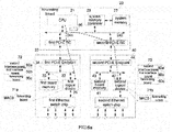
- the first logical device 32 may maintain a mapping table 71a, which is between an Ethernet MAC address and a board ID.
- the second logical device 42 may maintain a mapping table 71b, which is between an Ethernet MAC address and a board ID. Subsequently, the first logical device 32 and the second logical device 42 may determine the destination board of Ethernet data packet 51, or 52, or 53, or 54, based on the destination MAC address of the Ethernet data packet 51, or 52, or 53, or 54.
- the first logical device 32 and the second logical device 42 may also maintain a mapping table 72, which is between a board ID and a PCI-E memory space address, so as to determine the destination address of PCI-E packet 61, or 62, or 63, or 64 encapsulated with the Ethernet data packet 51, or 52, or 53, or 54, based on the destination board of the Ethernet data packet 51, or 52, or 53, or 54.
- a mapping table 72 which is between a board ID and a PCI-E memory space address, so as to determine the destination address of PCI-E packet 61, or 62, or 63, or 64 encapsulated with the Ethernet data packet 51, or 52, or 53, or 54, based on the destination board of the Ethernet data packet 51, or 52, or 53, or 54.
- FIG.6a illustrates the states of mapping tables 71a, 71b and 72, after initializing the network device 10.
- entries in the mapping tables 71a and 71b corresponding to the forwarding board 20, and all the entries in the mapping table 72 may be issued by the CPU 21, by using the PCI-E packet 60, when initializing the network device 10.
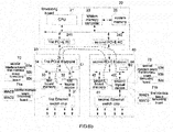
- "MAC0" shown in FIG.6a and FIG.6b represents the MAC address of the forwarding board 20.
- the PCI-E packet 60 for issuing an entry by the CPU 21 may be forwarded, by using the first PCI-E bus 11 and the second PCI-E bus 12. That is, the CPU 21 may reuse the first PCI-E bus 11 and the second PCI-E bus 12 to be a management bus, which is configured to issue an entry. It may be understood that, the management bus dedicated for issuing an entry, which is independent of the first PCI-E bus 11 and the second PCI-E bus 12, may be set within the network device 10. At this time, the issued entry may be carried by a protocol packet of an independent management bus.
- the entry in the mapping table 71a corresponding to the second interface board 40 may be learn by the first logical device 32 from the Ethernet data packet 52, which is encapsulated into the PCI-E packet 62 coming from the second interface board 40.
- "MAC2" in FIG.6b may represent the source MAC address of the Ethernet data packet 52.
- the entry in the mapping table 71b corresponding to the first interface board 30 may be learned by the second logical device 42 from the Ethernet data packet 51, which is encapsulated into the PCI-E packet 61 coming from the first interface board 30.
- "MAC1" in FIG.6b may represent the source MAC address of the Ethernet data packet 51.
- the first logical device 32 may obtain the PCI-E packet 62 from the first board memory 33.
- the PCI-E packet 62 may be encapsulated with the Ethernet data packet 52, which is received by the second logical device 42 through the second Ethernet switch chip 41.
- the PCI-E packet 62 may further carry the board ID of the second interface board 40.
- the first logical device 32 may create an entry corresponding to the second interface board 40 in the mapping table 71a, based on the source MAC address of the Ethernet data packet 52 analyzed from the PCI-E packet 62 and the board ID carried by the PCI-E packet 62.
- the second logical device 42 may obtain the PCI-E packet 61 from the second board memory 43.
- the PCI-E packet 61 may be encapsulated with the Ethernet data packet 51, which is received by the first logical device 32 from the first Ethernet switch chip 31.
- the PCI-E packet 61 may further carry the board ID of the first interface board 30.
- the second logical device 42 may create an entry corresponding to the first interface board 30 in the mapping table 71b, based on the source MAC address of the Ethernet data packet 51 analyzed from the PCI-E packet 61 and the board ID carried by the PCI-E packet 61.
- the first logical device 32 or the second logical device 42 may not search out a destination board of an Ethernet data packet, based on the mapping table between an Ethernet MAC address and a board ID.
- the destination board of the Ethernet data packet 51 may not be determined, by using the mapping table between the Ethernet MAC address and board ID. Subsequently, query the destination board for the Ethernet data packet 51 may be failed.
- the PCI-E packet may be forwarded one by one to the other interface boards except for the interface board.
- ID "51" may be different from foregoing Ethernet data packet 51.
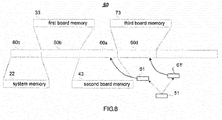
- a network device 10' may further include a third interface board 80.
- the third interface board 80 may include a third PCI-E Endpoint 84 and a third board memory 83.
- a forwarding board 20' may further include a third PCI-E RC 243.
- the third PCI-E RC 243 may be connected with the third PCI-E Endpoint 84 through a third PCI-E bus 13. Similar to the first PCI-E RC 241 and second PCI-E RC 242, the third PCI-E RC 243 may be an independent entity with PCI-E RC, which may also be an equivalent PCI-E RC formed logically.
- the third board memory 83 may map to the PCI-E memory space 60.
- an address range 60d in the PCI-E memory space 60 mapped by the third board memory 83 may be different from address ranges 60c, 60b and 60a in the PCI-E memory space, which are respectively mapped by the system memory 22, the first board memory 33 and the second board memory 43.
- the board ID issued by the CPU 21 when being initialized, and all the entries in the mapping table 72, which is between a PCI-E memory space address and a board ID, may further include an entry corresponding to the third interface board 80.
- the third PCI-E RC 243 and the third PCI-E Endpoint 84 may also be mapped to the PCI-E memory space 60.
- FIG.9 Please refer to FIG.9 and take into account FIG.8 :
- the first logical device 32 may determine the destination board of the Ethernet data packet 51, by matching an entry in the mapping table 71a; when not matching an entry in the mapping table 71a, that is, the first logical device 32 may determine that the forwarding board 20 is not the destination board of the Ethernet data packet 51 (for example, the mapping table 71a has an initial entry of MAC0 corresponding to the forwarding board 20), at this time, the destination MAC of the Ethernet data packet 51 may be a boardcast address.
- the first logical device 32 may encapsulate the Ethernet data packet 51 into PCI-E packets 61 and 61', which respectively take the PCI-E memory space address of the second board memory 43 (that is, address within the address range 60a shown in FIG.8 ) and the PCI-E memory space address of the third board memory 83 (that is, address within the address range 60d shown in FIG.8 ), based on the mapping table 72, such that the first PCI-E Endpoint 34 may transmit the PCI-E packets 61 and 61' to the first PCI-E RC 241, and enable the first PCI-E RC 241 to respectively forward the PCI-E packets 61 and 61' to the second PCI-E RC 242 and the third PCI-E RC 243, based on the destination addresses of the PCI-E packets 61 and 61'.
- the PCI-E packet 61 encapsulated with the Ethernet data packet 51 may arrive at the second interface board 40, and enable the second logical device 42 in the second interface board 40 to create an entry corresponding to the first interface board in the mapping table 71b.
- the PCI-E packet 61' may arrive at the third interface board 80.
- the third interface board 80 may possess a device similar to the first logical device 32 or the second logical device 42 (not shown in FIG.7 and FIG.9 ). The device may analyze the Ethernet data packet 51, and create an entry corresponding to the first interface board 30 in the mapping table between an Ethernet MAC address and a board ID.
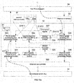
- the first logical device 32 may include an Ethernet bus controller 320, an Ethernet packet receiving and processing module 321, a first-mapping-table maintaining module 322, a PCI-E packet transmitting and processing module 323, a second-mapping-table maintaining module 324, a PCI-E packet receiving and processing module 325, an Ethernet packet transmitting and processing module 326 and a CPU switch register 327.
- working principle of the first logical device 32 may be as follows (since processing methods for the Ethernet data packets 51 and 53 in the first logical device 32 are basically the same, and processing methods for the PCI-E packets 61 and 63 in the first logical device 32 are basically the same, to simplify the view, the Ethernet data packet 53 and the PCI-E packet 63 are omitted in FIG.11 ):
- the Ethernet bus controller 320 may be connected with the first Ethernet switch chip 31 of the interface board, such that Ethernet data packets 51 and 52 may be interacted bewteen the first logical device 32 and the first Ethernet switch chip 31.
- the Ethernet packet receiving and processing module 321 may receive the Ethernet data packet 51 from the first Ethernet switch chip 31 via the Ethernet bus controller 320.
- the first-mapping-table maintaining module 322 may maintain a mapping table 71a, which is between an Ethernet MAC address and a board ID, such that the Ethernet packet receiving and processing module 321 may determine the destination board of the Ethernet data packet 51, by matching an entry in the mapping table 71a.
- the Ethernet packet receiving and processing module 321 may transmit the Ethernet data packet 51 and a matching result to the PCI-E packet transmitting and processing module 323.
- the matching result here may be a board ID of a destination board matched successfully, or a failed matching.
- the matching result may be the board ID of the matched second interface board 40 (denoted with S1111 in FIG.11 ).
- the PCI-E packet transmitting and processing module 323 may encapsulate the received Ethernet data packet 51.
- the second-mapping-table maintaining module 324 may maintain a mapping table 72, which is between a board ID and a PCI-E memory space address, such that the PCI-E packet transmitting and processing module 323 may determine the destination address of the encapsulated PCI-E packet 61, by matching an entry in the mapping table 72.
- the PCI-E packet transmitting and processing module 323 may encapsulate the Ethernet data packet 51 into the PCI-E packet 61, determine the destination address of the PCI-E packet 61 based on the matching result, and then, provide the PCI-E packet 61 to the first PCI-E Endpoint 34.
- the matching result here may be a board ID of a determined destination board, or board IDs of all the remaining interface boards (when not determining the destination board), in the example illustrated with FIG.11 , the address range of the matched second board memory 43 is 60a (denoted with S1112 and S1113 in FIG.11 ).
- the first-mapping-table maintaining module 322 may maintain entries corresponding to all the other interface boards (that is, the second interface board 40 and the third interface board 80) except for the first interface board 30 in the network device 10; the Ethernet packet receiving and processing module 321 may report all the other interface boards except for the first interface board 30 in the network device 10 to the PCI-E packet transmitting and processing module 323, such that the PCI-E packet transmitting and processing module 323 may match all the entries of the other interface boards except for the first interface board 30 one by one; in another example, the Ethernet packet receiving and processing module 321 may report a notification about failed matching to the PCI-E packet transmitting and processing module 323, such that the PCI-E packet transmitting and processing module 323 may poll entries of all the other interface boards except for the first interface board 30.
- the CPU switch register 327 may store the board ID of the first interface board, which is issued by the CPU 21.
- the PCI-E packet transmitting and processing module 323 may encapsulate the board ID of the first interface board into the PCI-E packet 61 (denoted with S1114 in FIG.11 ), such that another interface board (includes, but is not limited to, the second interface board 40) receiving the PCI-E packet 61 may learn a mapping entry corresponding to the first interface board, which is between an Ethernet MAC address and a board ID, by using the board ID of the first interface board and the source MAC address of the Ethernet data packet 51.
- the PCI-E packet receiving and processing module 325 may read PCI-E packets 60 and 62 from the first board memory 33, in which the PCI-E packets 60 and 62 respectively take the first interface board as the destination board.
- the PCI-E packet receiving and processing module 325 may analyze entries from the PCI-E packet 60, which are issued by the CPU 21 when initializing the network device 10, and write the entries into the first-mapping-table maintaining module 322 and the second-mapping-table maintaining module 324 (denoted with S1121 in FIG.11 ). Besides, the PCI-E packet receiving and processing module 325 may analyze the board ID of the first interface board from the PCI-E packet 60, which is issued by the CPU 21 when initializing the network device 10, and write the board ID of the first interface board into the CPU switch register 327 (denoted with S1122 in FIG.11 ).
- the PCI-E packet receiving and processing module 325 may analyze the PCI-E packet 62, and obtain the Ethernet data packet 52 coming from the second interface board 40 and the board ID of the second interface board 40, forward the obtained Ethernet data packet 52 and the board ID of the second interface board 40 to the Ethernet packet transmitting and processing module 326.
- the Ethernet packet transmitting and processing module 326 may extract the source MAC address from the received Ethernet data packet 52, and create an entry corresponding to the second interface board 40 in the first-mapping-table maintaining module 322, by using the extracted source MAC address and the received board ID of the second interface board 40.
- the Ethernet packet transmitting and processing module 326 may also transmit the received Ethernet data packet 52 to the Ethernet bus controller 320.
- the second logical device 42 may possess a structure simiar to that of the first logical device 32.
- the address range 60a in the PCI-E memory space 60 mapped by the second board memory 43 may include multiple data packet buffers 60a_1 ⁇ 60a_m (m is a positive integer greater than 1), and at least one control packet buffer 60a_ctr.
- the address range 60b in the PCI-E memory space 60 mapped by the first board memory 33 may include multiple data packet buffers 60b_1 ⁇ 60b_n (n is a positive integer greater than 1), and at least one control packet buffer 60b_ctr.
- the mapping table 72 between a board ID and a PCI-E memory space address, which is maintained by the first logical device 32, may include an entry 91 corresponding to the second interface board 40.
- the entry 91 may be divided into various sub-entries corresponding to multiple data packet buffers 60a_1 ⁇ 60a_m.
- each sub-entry may possess a Flag, which may represent whether state of a data packet buffer 60a_i (i is a positive integer greater than or equal to 1, meanwhile i is less than or equal to m) corresponding to the sub-entry is occupied or idle.
- the mapping table 72 between a board ID and a PCI-E memory space address, which is maintained by the second logical device 42, may include an entry 92 corresponding to the first interface board 30.
- the entry 92 may be divided into multiple sub-entries, which may respectively correspond to multiple data packet buffers 60b_1 ⁇ 60b_n.
- each sub-entry may possess a Flag, which may represent whether state of a data packet buffer 60b_j(j is a positive integer greater than or equal to 1, meanwhile j is less than or equal to n) corresponding to the sub-entry is occupied or idle.
- control packet buffers 60a_ctr and 60b_ctr may be taken as sub-entries without Flag in the mapping table 72, or, may be stored independent of the mapping table 72.
- FIG.13a in a case where forwarding is performed from the first interface board 30 to the second interface board 40: when the first logical device 32 in the first interface board 30 receives the Ethernet data packet 51 from the first Ethernet switch chip 31, the first logical device 32 may determine the destination board of the Ethernet data packet 51.
- the first logical device 32 may select an idle data packet buffer 60a_i from multiple data packet buffers 60a_1 ⁇ 60a_m, which are in the PCI-E memory space 60 mapped by the second board memory 43, and set Flag of a sub-entry corresponding to the data packet buffer 60a_i to be occupied, and then, encapsulate the Ethernet data packet 51 into a PCI-E packet 61, which takes the PCI-E memory space address of the data packet buffer 60a_i as destination address, such that the first PCI-E Endpoint 34 may transmit the PCI-E packet 61 to the first PCI-E RC 241, and the first PCI-E RC 241 may forward the PCI-E packet 61 to the second PCI-E RC 242, based on the destination address of the PCI-E packet 61.
- the destination address of the PCI-E packet 61 which is set by the first logical device 32, may be the PCI-E memory space address of the idle data packet buffer 60a_i mapped by the second board memory 43.
- the second logical device 42 may obtain the PCI-E packet 61 from the second board memory 43, analyze the Ethernet data packet 51 from the PCI-E packet 61, and transmit the Ethernet data packet 51 to the second Ethernet switch chip 41, such that the second Ethernet switch chip 41 may forward the Ethernet data packet 51 to the exterior of the network device 10.
- the second logical device 42 may also create a PCI-E packet 65, which takes the control packet buffer 60b_ctr as the destination address, such that the second PCI-E Endpoint 44 may transmit the PCI-E packet 65 to the second PCI-E RC 242. And then, the second PCI-E RC 242 may forward the PCI-E packet 65 to the first PCI-E RC 241, based on the destination address of the PCI-E packet 65.
- the PCI-E packet 65 may also carry release information of data packet buffer, which indicates to release the data packet buffer 60a_i.
- the first logical device 32 may obtain the PCI-E packet 65 from the first board memory 33, analyze the release information of data packet buffer from the PCI-E packet 65, so as to set Flag of the sub-entry corresponding to the data packet buffer 60a_i to be idle, based on the release information of data packet buffer.
- the destination address of the PCI-E packet 62 which is set by the second logical device 42, may be PCI-E memory space address of an idle data packet buffer 60b_j mapped by the first board memory 33.
- the second logical device 42 may set the Flag of the sub-entry corresponding to the data packet buffer 60b_j to be occupied.
- the first logical device 32 may also create a PCI-E packet 66, which takes the control packet buffer 60a_ctr as the destination address, such that the second logical device 42 may set the Flag of the sub-entry corresponding to the control mapped buffer 60a_ctr to be idle.
- an anti-pressure flow control may be performed to the forwarding of an Ethernet data packet between the first interface board 30 and the second interface board 40.
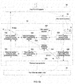
- the first logical device 32 may further include a release executing module 328 and a release informing module 329.
- the PCI-E packet transmitting and processing module 323 may set the Flag of a sub-entry corresponding to the data packet buffer 60a_i to be occupied (denoted with S1411 in FIG.15a ).
- the PCI-E packet receiving and processing module 325 may analyze the release information of data packet buffer from the PCI-E packet 65, and provide for the release executing module 328.
- the release executing module 328 may set the Flag of the sub-entry corresponding to the data packet buffer 60a_i to be idle (denoted with S1412 in FIG.15a ), based on the release information of data packet buffer provided by the PCI-E packet receiving and processing module 325.
- the PCI-E packet receiving and processing module 325 may analyze the Ethernet data packet 52 from the PCI-E packet 62, extract the destination address of the PCI-E packet 62 and carried board ID of the second interface board 40, and provide for the Ethernet packet transmitting and processing module 326. Subsequently, when transmitting the Ethernet data packet 52, the Ethernet packet transmitting and processing module 326 may provide the destination address of the PCI-E packet 62 and the board ID of the second interface board 40 to the release informing module 329.
- the release informing module 329 may inform the PCI-E packet transmitting and processing module 323 to create a PCI-E packet 66, which corresponds to the control packet buffer 60a_ctr of the second interface board 40, based on the destination address of the PCI-E packet 62 and board ID of the second interface board 40, and enable the PCI-E packet 66 to carry the destination address of the PCI-E packet 62 (that is, the PCI-E memory space address of the data packet buffer 60b_j), which is taken as the release information of data packet buffer.
- the method for forwarding packets may include the following blocks, which are executed by the first logical device 32 or the second logical device 42.
- the method may further include: encapsulate the Ethernet data packet into the PCI-E packet, which takes the PCI-E memory space address of the system memory as the destination address, such that the PCI-E Endpoint may forward the PCI-E packet to the forwarding board, and write the PCI-E packet into the system memory of the forwarding board.
- the method may further maintain a mapping table between a board ID and a PCI-E memory space address, so as to dertermine the destination address of the PCI-E packet encapsulated with the Ethernet data packet, based on the destination board of the Ethernet data packet received from the Ethernet switch chip; besides, create an entry in the second mapping table, based on configurations of the CPU in the forwarding board.
- the method may further maintain a mapping table between an Ethernet MAC address and a board ID.
- the method may analyze the Ethernet data packet (received from exterior of the network device) from the PCI-E packet received from another interface board, and board ID of the another interface board, and create an entry corresponding to the another interface board in the second mapping table, based on source MAC address of the analyzed Ethernet data packet and board ID carried by the PCI-E packet.
- the method further match an entry corresponding to the forwarding board in a first mapping table, which is between an Ethernet MAC address and a board ID, based on configurations of the CPU when initializing the network device.
- a first mapping table which is between an Ethernet MAC address and a board ID
- the method may further include: encapsulate the Ethernet data packet into at least two PCI-E packets, which respectively take PCI-E memory space address of board memory of each remaining interface board in the network device as destination address, such that the PCI-E Endpoint may forward the at least two PCI-E packets to the forwarding board, and enable the forwarding board to respectively forward the at least two PCI-E packets to corresponding other interface boards, based on the destination addresses of the at least two PCI-E packets.
- an anti-pressure flow control mechanism simitar with the principle of FIG.12 may also be applied, correspondingly:
- the address range in the PCI-E memory space mapped by board memory of each interface board may include multiple data packet buffers, and at least one control packet buffer. Besides, the method may further include:
- the destination board of the Ethernet data packet received from the Ethernet switch chip is another interface board (such as the second interface board)
- create a third PCI-E packet carrying release information of a data packet buffer may take the control packet buffer mapped by board memory of the third interface board as destination address, such that the PCI-E Endpoint may forward the created third PCI-E packet to the forwarding board, and enable the forwarding board to forward the third PCI-E packet to the third interface board, based on destination address of the created third PCI-E packet.
- the logical device of the interface board may encapsulate the Ethernet data packet into a PCI-E packet, which takes PCI-E memory space address of board memory of the another interface board as destination address, such that the PCI-E packet may be forwarded by the forwarding board to the board memory of the another interface board.
- the logical device in the interface board may analyze the Ethernet data packet from the PCI-E packet, and forward the Ethernet data packet. Subsequently, it is not necessary for the CPU to participate in the forwarding of the Ethernet data packet between interface boards, thereby improving forwarding performance.
Landscapes
- Engineering & Computer Science (AREA)
- Theoretical Computer Science (AREA)
- General Engineering & Computer Science (AREA)
- Physics & Mathematics (AREA)
- General Physics & Mathematics (AREA)
- Computer Networks & Wireless Communication (AREA)
- Signal Processing (AREA)
- Computer Hardware Design (AREA)
- Data Exchanges In Wide-Area Networks (AREA)
- Information Transfer Systems (AREA)
- Small-Scale Networks (AREA)
Applications Claiming Priority (2)
| Application Number | Priority Date | Filing Date | Title |
|---|---|---|---|
| CN201510721081.9A CN106713183B (zh) | 2015-10-30 | 2015-10-30 | 网络设备的接口板以及该网络设备和报文转发方法 |
| PCT/CN2016/103943 WO2017071667A1 (zh) | 2015-10-30 | 2016-10-31 | 报文转发 |
Publications (3)
| Publication Number | Publication Date |
|---|---|
| EP3370377A1 true EP3370377A1 (de) | 2018-09-05 |
| EP3370377A4 EP3370377A4 (de) | 2018-11-07 |
| EP3370377B1 EP3370377B1 (de) | 2019-11-27 |
Family
ID=58631397
Family Applications (1)
| Application Number | Title | Priority Date | Filing Date |
|---|---|---|---|
| EP16859102.2A Active EP3370377B1 (de) | 2015-10-30 | 2016-10-31 | Paketweiterleitung |
Country Status (5)
| Country | Link |
|---|---|
| US (1) | US10430364B2 (de) |
| EP (1) | EP3370377B1 (de) |
| JP (1) | JP6592599B2 (de) |
| CN (1) | CN106713183B (de) |
| WO (1) | WO2017071667A1 (de) |
Families Citing this family (5)
| Publication number | Priority date | Publication date | Assignee | Title |
|---|---|---|---|---|
| CN108737296B (zh) | 2017-09-27 | 2020-12-04 | 新华三技术有限公司 | 一种数据传输方法、装置和网络设备 |
| CN112910783B (zh) * | 2019-11-19 | 2024-02-27 | 中兴通讯股份有限公司 | 一种报文转发方法、装置及分布式设备 |
| US11803503B2 (en) | 2021-07-08 | 2023-10-31 | Mediatek Inc. | Chip having dual-mode device that switches between root complex mode and endpoint mode in different system stages and associated computer system |
| CN114553797B (zh) * | 2022-02-25 | 2023-05-09 | 星宸科技股份有限公司 | 具有命令转发机制的多芯片系统及地址产生方法 |
| CN117499346B (zh) * | 2023-12-28 | 2024-03-01 | 苏州元脑智能科技有限公司 | 访问控制信息的下发方法及装置 |
Family Cites Families (22)
| Publication number | Priority date | Publication date | Assignee | Title |
|---|---|---|---|---|
| US5566170A (en) * | 1994-12-29 | 1996-10-15 | Storage Technology Corporation | Method and apparatus for accelerated packet forwarding |
| US7830882B2 (en) * | 2006-11-17 | 2010-11-09 | Intel Corporation | Switch scaling for virtualized network interface controllers |
| CN101277195B (zh) * | 2007-03-30 | 2011-12-07 | 杭州华三通信技术有限公司 | 一种交换网通信系统、实现方法及交换装置 |
| US8503468B2 (en) * | 2008-11-05 | 2013-08-06 | Fusion-Io, Inc. | PCI express load sharing network interface controller cluster |
| US9306849B2 (en) * | 2010-05-03 | 2016-04-05 | Pluribus Networks, Inc. | Methods and systems for managing distribute media access control address tables |
| JP5613517B2 (ja) | 2010-09-30 | 2014-10-22 | 京セラドキュメントソリューションズ株式会社 | 情報処理装置 |
| CN102393838B (zh) * | 2011-07-04 | 2015-03-11 | 华为技术有限公司 | 数据处理方法及装置、pci-e总线系统、服务器 |
| US8661178B2 (en) | 2011-07-27 | 2014-02-25 | Agilent Technologies, Inc. | PCI-E system having reconfigurable link architecture |
| JP2013088879A (ja) | 2011-10-13 | 2013-05-13 | Kyocera Document Solutions Inc | 情報処理装置 |
| WO2013157256A1 (ja) | 2012-04-18 | 2013-10-24 | 日本電気株式会社 | インターワーク装置、方法、及びプログラムを格納した非一時的なコンピュータ可読媒体 |
| US9178815B2 (en) * | 2013-03-05 | 2015-11-03 | Intel Corporation | NIC flow switching |
| JP6070357B2 (ja) * | 2013-03-28 | 2017-02-01 | 富士通株式会社 | ストレージ装置 |
| US9244874B2 (en) * | 2013-06-14 | 2016-01-26 | National Instruments Corporation | Selectively transparent bridge for peripheral component interconnect express bus systems |
| US9135200B2 (en) * | 2013-06-28 | 2015-09-15 | Futurewei Technologies, Inc. | System and method for extended peripheral component interconnect express fabrics |
| US10684973B2 (en) * | 2013-08-30 | 2020-06-16 | Intel Corporation | NUMA node peripheral switch |
| CN103490961B (zh) * | 2013-09-05 | 2017-05-10 | 新华三技术有限公司 | 一种网络设备 |
| KR101670342B1 (ko) * | 2013-10-29 | 2016-10-28 | 후아웨이 테크놀러지 컴퍼니 리미티드 | 데이터 처리 시스템 및 데이터 처리 방법 |
| JP6197674B2 (ja) | 2014-01-31 | 2017-09-20 | 富士通株式会社 | 通信方法、中継装置、および、通信プログラム |
| US9753883B2 (en) * | 2014-02-04 | 2017-09-05 | Netronome Systems, Inc. | Network interface device that maps host bus writes of configuration information for virtual NIDs into a small transactional memory |
| US9886410B1 (en) * | 2015-02-04 | 2018-02-06 | Amazon Technologies, Inc. | Dynamic function assignment to I/O device interface port |
| CN107241913B (zh) * | 2015-02-25 | 2020-06-19 | 株式会社日立制作所 | 信息处理装置 |
| US10073805B2 (en) * | 2015-09-03 | 2018-09-11 | Avago Technologies General Ip (Singapore) Pte. Ltd. | Virtual expansion ROM in a PCIe environment |
-
2015
- 2015-10-30 CN CN201510721081.9A patent/CN106713183B/zh active Active
-
2016
- 2016-10-31 EP EP16859102.2A patent/EP3370377B1/de active Active
- 2016-10-31 JP JP2018521989A patent/JP6592599B2/ja active Active
- 2016-10-31 WO PCT/CN2016/103943 patent/WO2017071667A1/zh not_active Ceased
- 2016-10-31 US US15/771,963 patent/US10430364B2/en active Active
Also Published As
| Publication number | Publication date |
|---|---|
| EP3370377B1 (de) | 2019-11-27 |
| CN106713183B (zh) | 2020-03-17 |
| US10430364B2 (en) | 2019-10-01 |
| CN106713183A (zh) | 2017-05-24 |
| JP6592599B2 (ja) | 2019-10-16 |
| JP2018533794A (ja) | 2018-11-15 |
| EP3370377A4 (de) | 2018-11-07 |
| US20180225247A1 (en) | 2018-08-09 |
| WO2017071667A1 (zh) | 2017-05-04 |
Similar Documents
| Publication | Publication Date | Title |
|---|---|---|
| US12341686B2 (en) | System and method for facilitating efficient utilization of an output buffer in a network interface controller (NIC) | |
| EP3370377B1 (de) | Paketweiterleitung | |
| CN104424105B (zh) | 一种内存数据的读写处理方法和装置 | |
| US10333845B2 (en) | Forwarding data packets | |
| CN103828332B (zh) | 数据处理方法、装置、存储控制器和机柜 | |
| WO2018192587A1 (zh) | 一种查表方法及装置、计算机存储介质 | |
| US8472420B2 (en) | Gateway device | |
| US20150242535A1 (en) | Content Searching Chip and System Based on Peripheral Component Interconnect Bus | |
| WO2015184706A1 (zh) | 统计计数设备及其实现方法、具有统计计数设备的系统 | |
| CN101895397A (zh) | 一种基于dsp的工业以太网串口服务器及其控制方法 | |
| CN105099959A (zh) | 一种多播包的转发方法、设备和系统 | |
| US20260121999A1 (en) | Network interface card device, network data transmission method, apparatus, and system, device, and medium | |
| CN113746692A (zh) | 网络流量统计的方法、电子设备及存储介质 | |
| CN104584492B (zh) | 报文处理方法、设备及系统 | |
| CN108667732A (zh) | 一种报文转发方法及装置 | |
| CN113328870B (zh) | 一种多协议混合网络的多节点并行工作方法 | |
| CN116545932A (zh) | 网卡的报文传输方法、装置、计算机设备及存储介质 | |
| CN101478462B (zh) | 存储数据读取和写入的装置和方法及固态硬盘 | |
| CN113014510A (zh) | 惯导系统分布式测试中数据缓存方法及装置 | |
| CN105592169B (zh) | 终端识别方法及装置 | |
| CN108259348A (zh) | 一种报文传输方法和装置 | |
| CN112637322B (zh) | 一种服务器与交换机端口连接信息的查询系统及方法 | |
| CN116320079A (zh) | 报文传输方法、装置、电子设备和存储介质 | |
| CN113328926A (zh) | 一种fc-ae-1553和fc-ae-asm的混合网络系统 | |
| CN105515856B (zh) | 基于通道的fc网络余度设计方法 |
Legal Events
| Date | Code | Title | Description |
|---|---|---|---|
| STAA | Information on the status of an ep patent application or granted ep patent |
Free format text: STATUS: THE INTERNATIONAL PUBLICATION HAS BEEN MADE |
|
| PUAI | Public reference made under article 153(3) epc to a published international application that has entered the european phase |
Free format text: ORIGINAL CODE: 0009012 |
|
| STAA | Information on the status of an ep patent application or granted ep patent |
Free format text: STATUS: REQUEST FOR EXAMINATION WAS MADE |
|
| 17P | Request for examination filed |
Effective date: 20180503 |
|
| AK | Designated contracting states |
Kind code of ref document: A1 Designated state(s): AL AT BE BG CH CY CZ DE DK EE ES FI FR GB GR HR HU IE IS IT LI LT LU LV MC MK MT NL NO PL PT RO RS SE SI SK SM TR |
|
| AX | Request for extension of the european patent |
Extension state: BA ME |
|
| A4 | Supplementary search report drawn up and despatched |
Effective date: 20181005 |
|
| RIC1 | Information provided on ipc code assigned before grant |
Ipc: G06F 13/40 20060101ALI20180929BHEP Ipc: H04L 12/931 20130101AFI20180929BHEP Ipc: G06F 13/42 20060101ALI20180929BHEP |
|
| DAV | Request for validation of the european patent (deleted) | ||
| DAX | Request for extension of the european patent (deleted) | ||
| GRAP | Despatch of communication of intention to grant a patent |
Free format text: ORIGINAL CODE: EPIDOSNIGR1 |
|
| STAA | Information on the status of an ep patent application or granted ep patent |
Free format text: STATUS: GRANT OF PATENT IS INTENDED |
|
| INTG | Intention to grant announced |
Effective date: 20190717 |
|
| GRAS | Grant fee paid |
Free format text: ORIGINAL CODE: EPIDOSNIGR3 |
|
| GRAA | (expected) grant |
Free format text: ORIGINAL CODE: 0009210 |
|
| STAA | Information on the status of an ep patent application or granted ep patent |
Free format text: STATUS: THE PATENT HAS BEEN GRANTED |
|
| AK | Designated contracting states |
Kind code of ref document: B1 Designated state(s): AL AT BE BG CH CY CZ DE DK EE ES FI FR GB GR HR HU IE IS IT LI LT LU LV MC MK MT NL NO PL PT RO RS SE SI SK SM TR |
|
| REG | Reference to a national code |
Ref country code: GB Ref legal event code: FG4D |
|
| REG | Reference to a national code |
Ref country code: CH Ref legal event code: EP |
|
| REG | Reference to a national code |
Ref country code: AT Ref legal event code: REF Ref document number: 1207978 Country of ref document: AT Kind code of ref document: T Effective date: 20191215 |
|
| REG | Reference to a national code |
Ref country code: DE Ref legal event code: R096 Ref document number: 602016025305 Country of ref document: DE |
|
| REG | Reference to a national code |
Ref country code: IE Ref legal event code: FG4D |
|
| REG | Reference to a national code |
Ref country code: NL Ref legal event code: MP Effective date: 20191127 |
|
| REG | Reference to a national code |
Ref country code: LT Ref legal event code: MG4D |
|
| PG25 | Lapsed in a contracting state [announced via postgrant information from national office to epo] |
Ref country code: NO Free format text: LAPSE BECAUSE OF FAILURE TO SUBMIT A TRANSLATION OF THE DESCRIPTION OR TO PAY THE FEE WITHIN THE PRESCRIBED TIME-LIMIT Effective date: 20200227 Ref country code: GR Free format text: LAPSE BECAUSE OF FAILURE TO SUBMIT A TRANSLATION OF THE DESCRIPTION OR TO PAY THE FEE WITHIN THE PRESCRIBED TIME-LIMIT Effective date: 20200228 Ref country code: NL Free format text: LAPSE BECAUSE OF FAILURE TO SUBMIT A TRANSLATION OF THE DESCRIPTION OR TO PAY THE FEE WITHIN THE PRESCRIBED TIME-LIMIT Effective date: 20191127 Ref country code: LT Free format text: LAPSE BECAUSE OF FAILURE TO SUBMIT A TRANSLATION OF THE DESCRIPTION OR TO PAY THE FEE WITHIN THE PRESCRIBED TIME-LIMIT Effective date: 20191127 Ref country code: LV Free format text: LAPSE BECAUSE OF FAILURE TO SUBMIT A TRANSLATION OF THE DESCRIPTION OR TO PAY THE FEE WITHIN THE PRESCRIBED TIME-LIMIT Effective date: 20191127 Ref country code: SE Free format text: LAPSE BECAUSE OF FAILURE TO SUBMIT A TRANSLATION OF THE DESCRIPTION OR TO PAY THE FEE WITHIN THE PRESCRIBED TIME-LIMIT Effective date: 20191127 Ref country code: BG Free format text: LAPSE BECAUSE OF FAILURE TO SUBMIT A TRANSLATION OF THE DESCRIPTION OR TO PAY THE FEE WITHIN THE PRESCRIBED TIME-LIMIT Effective date: 20200227 Ref country code: FI Free format text: LAPSE BECAUSE OF FAILURE TO SUBMIT A TRANSLATION OF THE DESCRIPTION OR TO PAY THE FEE WITHIN THE PRESCRIBED TIME-LIMIT Effective date: 20191127 |
|
| PG25 | Lapsed in a contracting state [announced via postgrant information from national office to epo] |
Ref country code: RS Free format text: LAPSE BECAUSE OF FAILURE TO SUBMIT A TRANSLATION OF THE DESCRIPTION OR TO PAY THE FEE WITHIN THE PRESCRIBED TIME-LIMIT Effective date: 20191127 Ref country code: HR Free format text: LAPSE BECAUSE OF FAILURE TO SUBMIT A TRANSLATION OF THE DESCRIPTION OR TO PAY THE FEE WITHIN THE PRESCRIBED TIME-LIMIT Effective date: 20191127 Ref country code: IS Free format text: LAPSE BECAUSE OF FAILURE TO SUBMIT A TRANSLATION OF THE DESCRIPTION OR TO PAY THE FEE WITHIN THE PRESCRIBED TIME-LIMIT Effective date: 20200327 |
|
| PG25 | Lapsed in a contracting state [announced via postgrant information from national office to epo] |
Ref country code: AL Free format text: LAPSE BECAUSE OF FAILURE TO SUBMIT A TRANSLATION OF THE DESCRIPTION OR TO PAY THE FEE WITHIN THE PRESCRIBED TIME-LIMIT Effective date: 20191127 |
|
| PG25 | Lapsed in a contracting state [announced via postgrant information from national office to epo] |
Ref country code: DK Free format text: LAPSE BECAUSE OF FAILURE TO SUBMIT A TRANSLATION OF THE DESCRIPTION OR TO PAY THE FEE WITHIN THE PRESCRIBED TIME-LIMIT Effective date: 20191127 Ref country code: PT Free format text: LAPSE BECAUSE OF FAILURE TO SUBMIT A TRANSLATION OF THE DESCRIPTION OR TO PAY THE FEE WITHIN THE PRESCRIBED TIME-LIMIT Effective date: 20200419 Ref country code: EE Free format text: LAPSE BECAUSE OF FAILURE TO SUBMIT A TRANSLATION OF THE DESCRIPTION OR TO PAY THE FEE WITHIN THE PRESCRIBED TIME-LIMIT Effective date: 20191127 Ref country code: RO Free format text: LAPSE BECAUSE OF FAILURE TO SUBMIT A TRANSLATION OF THE DESCRIPTION OR TO PAY THE FEE WITHIN THE PRESCRIBED TIME-LIMIT Effective date: 20191127 Ref country code: CZ Free format text: LAPSE BECAUSE OF FAILURE TO SUBMIT A TRANSLATION OF THE DESCRIPTION OR TO PAY THE FEE WITHIN THE PRESCRIBED TIME-LIMIT Effective date: 20191127 Ref country code: ES Free format text: LAPSE BECAUSE OF FAILURE TO SUBMIT A TRANSLATION OF THE DESCRIPTION OR TO PAY THE FEE WITHIN THE PRESCRIBED TIME-LIMIT Effective date: 20191127 |
|
| REG | Reference to a national code |
Ref country code: DE Ref legal event code: R097 Ref document number: 602016025305 Country of ref document: DE |
|
| PG25 | Lapsed in a contracting state [announced via postgrant information from national office to epo] |
Ref country code: SM Free format text: LAPSE BECAUSE OF FAILURE TO SUBMIT A TRANSLATION OF THE DESCRIPTION OR TO PAY THE FEE WITHIN THE PRESCRIBED TIME-LIMIT Effective date: 20191127 Ref country code: SK Free format text: LAPSE BECAUSE OF FAILURE TO SUBMIT A TRANSLATION OF THE DESCRIPTION OR TO PAY THE FEE WITHIN THE PRESCRIBED TIME-LIMIT Effective date: 20191127 |
|
| REG | Reference to a national code |
Ref country code: AT Ref legal event code: MK05 Ref document number: 1207978 Country of ref document: AT Kind code of ref document: T Effective date: 20191127 |
|
| PLBE | No opposition filed within time limit |
Free format text: ORIGINAL CODE: 0009261 |
|
| STAA | Information on the status of an ep patent application or granted ep patent |
Free format text: STATUS: NO OPPOSITION FILED WITHIN TIME LIMIT |
|
| 26N | No opposition filed |
Effective date: 20200828 |
|
| PG25 | Lapsed in a contracting state [announced via postgrant information from national office to epo] |
Ref country code: PL Free format text: LAPSE BECAUSE OF FAILURE TO SUBMIT A TRANSLATION OF THE DESCRIPTION OR TO PAY THE FEE WITHIN THE PRESCRIBED TIME-LIMIT Effective date: 20191127 Ref country code: SI Free format text: LAPSE BECAUSE OF FAILURE TO SUBMIT A TRANSLATION OF THE DESCRIPTION OR TO PAY THE FEE WITHIN THE PRESCRIBED TIME-LIMIT Effective date: 20191127 Ref country code: AT Free format text: LAPSE BECAUSE OF FAILURE TO SUBMIT A TRANSLATION OF THE DESCRIPTION OR TO PAY THE FEE WITHIN THE PRESCRIBED TIME-LIMIT Effective date: 20191127 |
|
| PG25 | Lapsed in a contracting state [announced via postgrant information from national office to epo] |
Ref country code: IT Free format text: LAPSE BECAUSE OF FAILURE TO SUBMIT A TRANSLATION OF THE DESCRIPTION OR TO PAY THE FEE WITHIN THE PRESCRIBED TIME-LIMIT Effective date: 20191127 |
|
| REG | Reference to a national code |
Ref country code: CH Ref legal event code: PL |
|
| PG25 | Lapsed in a contracting state [announced via postgrant information from national office to epo] |
Ref country code: MC Free format text: LAPSE BECAUSE OF FAILURE TO SUBMIT A TRANSLATION OF THE DESCRIPTION OR TO PAY THE FEE WITHIN THE PRESCRIBED TIME-LIMIT Effective date: 20191127 Ref country code: LU Free format text: LAPSE BECAUSE OF NON-PAYMENT OF DUE FEES Effective date: 20201031 |
|
| REG | Reference to a national code |
Ref country code: BE Ref legal event code: MM Effective date: 20201031 |
|
| PG25 | Lapsed in a contracting state [announced via postgrant information from national office to epo] |
Ref country code: BE Free format text: LAPSE BECAUSE OF NON-PAYMENT OF DUE FEES Effective date: 20201031 Ref country code: CH Free format text: LAPSE BECAUSE OF NON-PAYMENT OF DUE FEES Effective date: 20201031 Ref country code: LI Free format text: LAPSE BECAUSE OF NON-PAYMENT OF DUE FEES Effective date: 20201031 |
|
| PG25 | Lapsed in a contracting state [announced via postgrant information from national office to epo] |
Ref country code: IE Free format text: LAPSE BECAUSE OF NON-PAYMENT OF DUE FEES Effective date: 20201031 |
|
| REG | Reference to a national code |
Ref country code: DE Ref legal event code: R079 Ref document number: 602016025305 Country of ref document: DE Free format text: PREVIOUS MAIN CLASS: H04L0012931000 Ipc: H04L0049100000 |
|
| PG25 | Lapsed in a contracting state [announced via postgrant information from national office to epo] |
Ref country code: TR Free format text: LAPSE BECAUSE OF FAILURE TO SUBMIT A TRANSLATION OF THE DESCRIPTION OR TO PAY THE FEE WITHIN THE PRESCRIBED TIME-LIMIT Effective date: 20191127 Ref country code: MT Free format text: LAPSE BECAUSE OF FAILURE TO SUBMIT A TRANSLATION OF THE DESCRIPTION OR TO PAY THE FEE WITHIN THE PRESCRIBED TIME-LIMIT Effective date: 20191127 Ref country code: CY Free format text: LAPSE BECAUSE OF FAILURE TO SUBMIT A TRANSLATION OF THE DESCRIPTION OR TO PAY THE FEE WITHIN THE PRESCRIBED TIME-LIMIT Effective date: 20191127 |
|
| PG25 | Lapsed in a contracting state [announced via postgrant information from national office to epo] |
Ref country code: MK Free format text: LAPSE BECAUSE OF FAILURE TO SUBMIT A TRANSLATION OF THE DESCRIPTION OR TO PAY THE FEE WITHIN THE PRESCRIBED TIME-LIMIT Effective date: 20191127 |
|
| P01 | Opt-out of the competence of the unified patent court (upc) registered |
Effective date: 20230424 |
|
| PGFP | Annual fee paid to national office [announced via postgrant information from national office to epo] |
Ref country code: GB Payment date: 20250922 Year of fee payment: 10 |
|
| PGFP | Annual fee paid to national office [announced via postgrant information from national office to epo] |
Ref country code: FR Payment date: 20250916 Year of fee payment: 10 |
|
| PGFP | Annual fee paid to national office [announced via postgrant information from national office to epo] |
Ref country code: DE Payment date: 20250122 Year of fee payment: 10 |