EP3370250A1 - Film mold and imprinting method - Google Patents
Film mold and imprinting method Download PDFInfo
- Publication number
- EP3370250A1 EP3370250A1 EP16859600.5A EP16859600A EP3370250A1 EP 3370250 A1 EP3370250 A1 EP 3370250A1 EP 16859600 A EP16859600 A EP 16859600A EP 3370250 A1 EP3370250 A1 EP 3370250A1
- Authority
- EP
- European Patent Office
- Prior art keywords
- layer
- film mold
- glass substrate
- resin composition
- pattern
- Prior art date
- Legal status (The legal status is an assumption and is not a legal conclusion. Google has not performed a legal analysis and makes no representation as to the accuracy of the status listed.)
- Granted
Links
Images



Classifications
-
- B—PERFORMING OPERATIONS; TRANSPORTING
- B32—LAYERED PRODUCTS
- B32B—LAYERED PRODUCTS, i.e. PRODUCTS BUILT-UP OF STRATA OF FLAT OR NON-FLAT, e.g. CELLULAR OR HONEYCOMB, FORM
- B32B17/00—Layered products essentially comprising sheet glass, or glass, slag, or like fibres
- B32B17/06—Layered products essentially comprising sheet glass, or glass, slag, or like fibres comprising glass as the main or only constituent of a layer, next to another layer of a specific material
- B32B17/10—Layered products essentially comprising sheet glass, or glass, slag, or like fibres comprising glass as the main or only constituent of a layer, next to another layer of a specific material of synthetic resin
-
- B—PERFORMING OPERATIONS; TRANSPORTING
- B29—WORKING OF PLASTICS; WORKING OF SUBSTANCES IN A PLASTIC STATE IN GENERAL
- B29C—SHAPING OR JOINING OF PLASTICS; SHAPING OF MATERIAL IN A PLASTIC STATE, NOT OTHERWISE PROVIDED FOR; AFTER-TREATMENT OF THE SHAPED PRODUCTS, e.g. REPAIRING
- B29C59/00—Surface shaping of articles, e.g. embossing; Apparatus therefor
- B29C59/02—Surface shaping of articles, e.g. embossing; Apparatus therefor by mechanical means, e.g. pressing
-
- B—PERFORMING OPERATIONS; TRANSPORTING
- B32—LAYERED PRODUCTS
- B32B—LAYERED PRODUCTS, i.e. PRODUCTS BUILT-UP OF STRATA OF FLAT OR NON-FLAT, e.g. CELLULAR OR HONEYCOMB, FORM
- B32B17/00—Layered products essentially comprising sheet glass, or glass, slag, or like fibres
- B32B17/06—Layered products essentially comprising sheet glass, or glass, slag, or like fibres comprising glass as the main or only constituent of a layer, next to another layer of a specific material
- B32B17/10—Layered products essentially comprising sheet glass, or glass, slag, or like fibres comprising glass as the main or only constituent of a layer, next to another layer of a specific material of synthetic resin
- B32B17/10005—Layered products essentially comprising sheet glass, or glass, slag, or like fibres comprising glass as the main or only constituent of a layer, next to another layer of a specific material of synthetic resin laminated safety glass or glazing
- B32B17/10009—Layered products essentially comprising sheet glass, or glass, slag, or like fibres comprising glass as the main or only constituent of a layer, next to another layer of a specific material of synthetic resin laminated safety glass or glazing characterized by the number, the constitution or treatment of glass sheets
- B32B17/10064—Layered products essentially comprising sheet glass, or glass, slag, or like fibres comprising glass as the main or only constituent of a layer, next to another layer of a specific material of synthetic resin laminated safety glass or glazing characterized by the number, the constitution or treatment of glass sheets comprising at least two glass sheets, only one of which being an outer layer
-
- G—PHYSICS
- G03—PHOTOGRAPHY; CINEMATOGRAPHY; ANALOGOUS TECHNIQUES USING WAVES OTHER THAN OPTICAL WAVES; ELECTROGRAPHY; HOLOGRAPHY
- G03F—PHOTOMECHANICAL PRODUCTION OF TEXTURED OR PATTERNED SURFACES, e.g. FOR PRINTING, FOR PROCESSING OF SEMICONDUCTOR DEVICES; MATERIALS THEREFOR; ORIGINALS THEREFOR; APPARATUS SPECIALLY ADAPTED THEREFOR
- G03F7/00—Photomechanical, e.g. photolithographic, production of textured or patterned surfaces, e.g. printing surfaces; Materials therefor, e.g. comprising photoresists; Apparatus specially adapted therefor
- G03F7/0002—Lithographic processes using patterning methods other than those involving the exposure to radiation, e.g. by stamping
-
- H—ELECTRICITY
- H10—SEMICONDUCTOR DEVICES; ELECTRIC SOLID-STATE DEVICES NOT OTHERWISE PROVIDED FOR
- H10P—GENERIC PROCESSES OR APPARATUS FOR THE MANUFACTURE OR TREATMENT OF DEVICES COVERED BY CLASS H10
- H10P76/00—Manufacture or treatment of masks on semiconductor bodies, e.g. by lithography or photolithography
-
- B—PERFORMING OPERATIONS; TRANSPORTING
- B29—WORKING OF PLASTICS; WORKING OF SUBSTANCES IN A PLASTIC STATE IN GENERAL
- B29K—INDEXING SCHEME ASSOCIATED WITH SUBCLASSES B29B, B29C OR B29D, RELATING TO MOULDING MATERIALS OR TO MATERIALS FOR MOULDS, REINFORCEMENTS, FILLERS OR PREFORMED PARTS, e.g. INSERTS
- B29K2709/00—Use of inorganic materials not provided for in groups B29K2703/00 - B29K2707/00, for preformed parts, e.g. for inserts
- B29K2709/08—Glass
Definitions
- Embodiments of the present disclosure relate to a film mold and an imprinting method.
- Imprinting is a pattern formation technique of, by using a mold having a pattern region including, for example, a fine concavo-convex pattern, transferring the concavo-convex pattern of the mold to a molding target material at the same magnification.
- imprinting using a photocurable resin composition as the molding target material is performed as follows. First, droplets of the photocurable resin composition are supplied to the surface of a transfer substrate. Next, the mold having the pattern region including a desired concavo-convex pattern and the transfer substrate are positioned in a predetermined state. Thereafter, the mold and the photocurable resin composition are brought into contact with each other to fill the concavo-convex pattern of the mold with the photocurable resin composition. In this state, light is radiated from the mold side to cure the photocurable resin composition, and thereby a resin layer is formed. Thereafter, the mold and the resin layer are pulled apart (mold releasing). Thereby, a pattern structure having a concavo-convex pattern in which the concavo-convex pattern in the pattern region of the mold is inverted is formed.
- Molds used for such imprinting is roughly divided into hard molds formed of glass, quartz or the like and molds having flexibility (hereinafter referred to as film molds).
- film molds examples of the advantage of using a film mold among these is that, as a result of releasing of the mold being easy, it is easy to increase the area of the pattern region and the transfer region of the molding target material on which the pattern region is inverted, that reproducibility is high because entrainment (inclusion) of bubbles can be suppressed easily, and that manufacture can be performed at low cost.
- various techniques have been proposed (for example, JP 5002422B , JP 5215833B , etc.).
- the conventional film mold is generally constituted by a resin composition, and its entirety and pattern are liable to be deformed due to its flexibility, material, and environmental factors such as temperature and humidity. Therefore, in the case where the film mold is deformed when positioning the film mold and the transfer substrate holding the molding target material in the predetermined state before the transfer, the film mold is undesirably displaced from the transfer substrate, and as a result, the positional accuracy of the pattern transferred onto the molding target material may be degraded in some cases. In particular, in the case of using imprinting in the manufacture of products in the fields of optics and semiconductors, the positional accuracy of the pattern transferred onto the molding target material greatly affects the performance of a finished product, and thus it is strongly desired to ensure good positional accuracy in the pattern to be transferred.
- Embodiments of the present disclosure have been made in view of the above circumstances, and it is an object of the present invention to provide a film mold and an imprinting method capable of transferring a pattern of good positional accuracy onto a molding target material.
- One embodiment of the present disclosure is a film mold including a first resin layer having a pattern region including a concavo-convex pattern and constituted by a resin composition, and a first glass substrate layer constituted by thin film glass and laminated on a surface on an opposite side to a surface on which the pattern region is formed in the first resin layer.
- the film mold according to one embodiment of the present disclosure may further include a second resin layer constituted by a resin composition and laminated on a surface on an opposite side to a surface on the first resin layer side of the first glass substrate layer.
- a contraction rate (shrinkage rate) of the resin composition constituting the first resin layer and a contraction rate (shrinkage rate) of the resin composition constituting the second resin layer may be the same.
- one of the resin composition constituting the first resin layer and the resin composition constituting the second resin layer may be a radically polymerizable curable resin composition and the other may be a cationically polymerizable curable resin composition.
- the first glass substrate layer may be formed of a material having a tensile stress of 50 MPa or lower when bent into a state of a curvature radius of 150 mm or smaller.
- the first glass substrate layer is formed of a material having a tensile stress of 50 MPa or lower when bent into a curvature radius of 75 mm or smaller.
- the film mold according to one embodiment of the present disclosure may further include a second glass substrate layer laminated on a surface on an opposite side to a surface on the first resin layer side of the first glass substrate layer via an intermediate layer, and the second glass substrate layer may be constituted by thin film glass.
- the first glass substrate layer and the second glass substrate layer may be formed of a material having a tensile stress of 50 MPa or lower when bent into a state of a curvature radius of 150 mm or smaller.
- the first glass substrate layer and the second glass substrate layer are formed of a material having a tensile stress of 50 MPa or lower when bent into a curvature radius of 75 mm or smaller.
- the first resin layer may have a non-pattern region in a region different from the pattern region, and an alignment mark may be provided in the non-pattern region.
- a Young's modulus of a layer formed of glass included in the film mold according to one embodiment of the present disclosure is 75 GPa or lower.
- one embodiment of the present disclosure is an imprinting method including a preparation step of preparing the film mold and a transfer substrate that holds a molding target material on one surface thereof, a positioning step of positioning the film mold and the transfer substrate in a predetermined state, a contact step of bringing the pattern region of the film mold into contact with the molding target material held on the transfer substrate, a curing step of curing the molding target material brought into contact with the film mold to form a transfer layer onto which a pattern corresponding to the pattern region has been transferred, and a release step of separating the transfer layer and the film mold from each other such that a pattern structure that is the transfer layer is positioned on the transfer substrate.
- FIG. 1 is a cross-sectional view of a film mold 1 according to a first embodiment.
- This film mold 1 can be used for manufacturing products in various fields, and can be suitably used for manufacturing various products in the fields of, for example, semiconductors, optical elements, biotechnology, and the like.
- the film mold 1 according to the first embodiment will be described in detail with reference to FIG. 1 .
- the film mold 1 includes a first resin layer 11 constituted by a resin composition and having a pattern region 11P including a concavo-convex pattern (unevenness pattern) and a non-pattern region 11N on one surface thereof, and a first glass substrate layer 12 constituted by thin film glass and laminated on the other surface of the first resin layer 11 on the side opposite to the one surface on which the pattern region 11P is provided.
- This film mold 1 has flexibility enough to be usable for imprinting by a roller transfer method, but may be also used for imprinting of a method different from the roller transfer method.
- a photocurable resin composition, a thermosetting resin composition, or a room-temperature curable resin composition is used in accordance with the formation method of the pattern region 11P. That is, in the first resin layer 11, the pattern region 11P is formed by contact with a concavo-convex pattern of a master (master mold), and the first resin layer 11 is fixed on the first glass substrate layer 12 by subsequent curing.
- a photocurable resin composition is used in the case where photocuring is carried out after the contact with the concavo-convex pattern of the master
- a thermosetting resin composition is used in the case where thermal curing is carried out
- a room temperature curable resin composition is used in the case where curing is carried out in room temperature.
- a photocurable resin composition is used as the resin composition constituting the first resin layer 11
- a radically polymerizable ultraviolet curable resin composition, a cationically polymerizable ultraviolet curable resin composition, or the like may be used.
- a material having heat resistance enough to allow baking treatment is used as the resin composition constituting the first resin layer 11.
- the process can be expected to be expanded and it is possible to improve the quality and the like, which is beneficial.
- the thickness of the first resin layer 11 is preferably 20 ⁇ m or smaller from the viewpoint of securing flexibility high enough to be used for imprinting by the roller transfer method.
- alignment marks 11A are provided in the non-pattern region 11N.
- the alignment marks 11A are formed, for example, in a concave shape, and it is preferable that a plurality of the alignment marks 11A are formed.
- the concavo-convex pattern of the pattern region 11P and the non-pattern region 11N of the first resin layer 11 are configured to come into contact with a molding target material 103 (see FIGS. 2 and 3 ) positioned on one surface 101a of, in other words, held by, a transfer substrate 101 that will be described later.
- a molding target material 103 positioned on one surface 101a of, in other words, held by, a transfer substrate 101 that will be described later.
- the film mold 1 and the transfer substrate 101 are positioned in a predetermined state.
- the alignment marks 11A at the time of this positioning, it can be confirmed whether or not the film mold 1 and the transfer substrate 101 are positioned in the predetermined state.
- the pattern region 11P refers to a part that transfers a pattern onto the molding target material 103 for the purpose of forming a pattern having a specific function on the molding target material 103, or for the purpose of forming an underlying part (resist pattern layer or the like) for forming a pattern having a specific function on the transfer substrate 101 on the molding target material 103.
- the non-pattern region 11N formed in a region different from the pattern region 11P refers to a part to be brought into contact with the molding target material 103 without the above-mentioned purpose.
- the first resin layer 11 has light transmittance such that the light transmittance at a wavelength of 200 to 400 nm is 70% or higher. Measurement of light transmittance can be performed using V-650 manufactured by JASCO Corporation.
- the material of the first glass substrate layer 12 is not particularly limited as long as the material is thin film glass.
- the thickness of the first glass substrate layer 12 is preferably 200 ⁇ m or smaller and more preferably about 100 ⁇ m from the viewpoint of securing flexibility high enough to be used for imprinting by the roller transfer method. More specifically, it is preferable that the first glass substrate layer 12 is formed of a glass material having a tensile stress of 50 MPa or lower when bent into a state with a curvature radius of 150 mm or smaller, and in particular, it is more preferable that the first glass substrate layer 12 is formed of a material having a tensile stress of 50 MPa or lower when bent into a state with a curvature radius of 75 mm or smaller.
- the breaking stress of glass is generally 50 MPa, and in the imprinting of the roller transfer method, the film mold is often bent to a curvature radius of 150 mm or smaller. Therefore, when the first glass substrate layer 12 is constituted by a material having a tensile stress of 50 MPa or lower when bent to a curvature radius of 150 mm or smaller, more preferably 75 mm or smaller, the film mold 1 can be effectively used in the imprinting of the roller transfer method.
- E is the Young's modulus (GPa)
- T is the thickness (mm) of the first glass substrate layer 12
- R is the curvature radius (mm).
- the Young's modulus of the glass material having a tensile stress of 50 MPa when bent into a state with a curvature radius of 150 mm and having a thickness of 200 ⁇ m is 75 GPa. Since the higher the Young's modulus is, the higher the tensile stress at bending is, the first glass substrate layer 12 is preferably formed of a material having a Young's modulus of 75 GPa or lower.
- the first glass substrate layer 12 has light transmittance such that the light transmittance at a wavelength of 200 to 400 nm is 70% or higher so that the molding target material 103 can be cured through the first glass substrate layer 12 and the first resin layer 11.
- the film mold 1 shown in FIG. 1 is prepared. Further, the transfer substrate 101 shown in FIG. 2(A) is prepared. In the transfer substrate 101, an etching target layer 102 is provided on one surface 101a of the transfer substrate 101, and the molding target material 103 is positioned on, in other words, held on, the etching target layer 102.
- the transfer substrate 101 used here can be appropriately selected and examples thereof include glasses such as quartz, soda-lime glass, and borosilicate glass; semiconductors such as silicon, gallium arsenide, and gallium nitride; resin substrates such as polycarbonate, polypropylene, and polyethylene; metal substrates; and composite material substrates constituted by a combination of these materials. Further, for example, a fine wiring used for a semiconductor, a display, or the like, or a desired pattern structure such as a photonic crystal structure or an optical structure such as an optical waveguide or holography may be formed therein.
- the etching target layer 102 may be a thin film made of a material required as a material of a pattern to be formed on the transfer substrate 101, and can be appropriately selected from, for example, an inorganic thin film, an organic thin film, and an organic/inorganic composite thin film, or the like.
- the molding target material 103 can be formed by a known coating means such as a spin coating method, a dispensing coating method, a dip coating method, a spray coating method, an inkjet method, or the like using, for example, a photocurable resin composition or a thermosetting resin composition. As described above, in the present embodiment, as an example, a photocurable resin composition is used as the molding target material 103.
- the thickness of the molding target material 103 can be determined in consideration of the height of a convex portion of the pattern region 11P of the film mold 1 to be used, the depth of a concave portion therebetween, and an acceptable range of the thickness of a residual film (position between the convex pattern) generated in a pattern structure to be formed, and the like.
- the film mold 1 and the transfer substrate 101 are positioned in a predetermined state. Specifically, in the present embodiment, the film mold 1 and the transfer substrate 101 are positioned such that a predetermined portion of the non-pattern region 11N of the film mold 1 is pressed against a predetermined portion of the transfer substrate 101 by a roller 151 shown in FIGS. 2(B) and 3(A) on a surface of the first glass substrate layer 12 opposite to the first resin layer 11 side of the film mold 1. In this state, the film mold 1 extends obliquely outward from the pressed portion. In the present embodiment, in this positioning, whether or not the predetermined portion of the non-pattern region 11N of the film mold 1 is accurately pressed against the predetermined portion of the transfer substrate 101 can be confirmed by using the alignment marks 11A.
- the pattern region 11P of the film mold 1 is continuously brought into contact with the molding target material 103 ( FIGS. 2(B) and 3(A) ) by conveying the transfer substrate 101 in the direction of arrow a shown in FIG. 2(B) and rotating the roller 151 in the direction of arrow b shown in FIG. 2(B) .
- the molding target material 103 in contact with the film mold 1 is cured, and thus a transfer layer 104 to which a pattern corresponding to the concavo-convex pattern of the pattern region 11P of the film mold 1 has been transferred is formed.
- the molding target material 103 immediately after being brought into contact with the film mold 1, the molding target material 103 is irradiated with light from a light irradiation device 161 via the film mold 1, and thus the molding target material 103 is cured to form the transfer layer 104. Therefore, in this example, the first resin layer 11 and the first glass substrate layer 12 have optical transparency.
- the transfer layer 104 may be formed by curing the molding target material 103 after the contact between the film mold 1 and the molding target material 103 is completed.
- the light irradiation device 161 may be disposed on the back side of the transfer substrate 101, and the molding target material 103 whose contact with the film mold 1 has been completed may be irradiated with light from the light irradiation device 161 through the transfer substrate 101 to cure the molding target material 103. Furthermore, curing of the molding target material 103 whose contact with the film mold 1 has been completed may be performed by using the light irradiation from the light irradiation device 161 through the film mold 1 and the light irradiation from the light irradiation device 161 through the transfer substrate 101 in combination.
- the pattern structure which is the transfer layer 104 is placed on the transfer substrate 101 ( FIGS. 2(C) and 3(B) ).
- This separation of the transfer layer 104 from the film mold 1 can be performed after the contact of the film mold 1 with the molding target material 103 and the formation of the transfer layer 104 by curing of the molding target material 103 are completed.
- the film mold 1 may be appropriately separated from the transfer layer 104 formed by curing the molding target material 103 which is already in contact with the film mold 1. Further, after the transfer layer 104 and the film mold 1 are separated from each other, additional exposure may be performed to completely cure the transfer layer 104.
- a desired pattern can be formed on the transfer substrate 101 by removing the residual film as necessary from the pattern of a pattern structure 104 that is the transfer layer 104 formed as described above and etching the etching target layer 102 by use the pattern structure 104 as a mask.
- a concavo-convex pattern can be also formed on the transfer substrate 101 by etching the transfer substrate 101 by using a pattern thus formed as a mask.
- the film mold 1 since good mechanical strength, heat resistance, and moisture resistance can be ensured by the first glass substrate layer 12, deformation caused by environmental factors such as the temperature and humidity at the time of and after manufacturing the film mold 1 can be prevented. As a result, at the time of positioning the transfer substrate 101, the film mold 1 being undesirably displaced with respect to the transfer substrate 101 due to the deformation can be prevented. Therefore, it is possible to transfer a pattern with good positional accuracy to the molding target material 103.
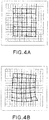
- FIG. 4A is a diagram exaggeratedly showing deviation between an actual pattern and a designed pattern
- the actual pattern in FIG.4A is a pattern that is transferred in the molding target material 103 by the imprinting method according to the first embodiment.
- FIG. 4B is a diagram exaggeratedly showing deviation between an actual pattern and a designed pattern
- the actual pattern in FIG.4B is a pattern that is transferred in a molding target material by an imprinting method using a conventional film mold (consisting of a resin composition).
- each intersection point of a lattice indicated by a bold line indicates an observed point of the actual pattern
- each intersection point of a lattice indicated by a thin line shows a comparison point of the designed pattern with respect to the observed point. More coincidence of observed point with the comparison point indicates higher positional accuracy of a pattern.
- FIGS. 4A and 4B in the case of using the film mold 1 according to the present embodiment, it can be seen that it is possible to transfer a pattern with good positional accuracy as compared with the case of a conventional film mold.
- the deviation between the observed point of the actual pattern and the comparison point of the designed pattern is about 2 ⁇ m at the maximum.
- the deviation in the case of the conventional film mold is about 9 ⁇ m at the maximum.
- a film mold 2 includes the first resin layer 11 and the first glass substrate layer 12 similar to those of the first embodiment, and a second resin layer 13 constituted by a resin composition and laminated on a surface of the first glass substrate layer 12 opposite to the surface on the first resin layer 11 side.
- the first glass substrate layer 12 is more likely to break when the thickness thereof is smaller.
- the second resin layer 13 functions as a protective layer for protecting the first glass substrate layer 12 as described above.
- the resin composition constituting the second resin layer 13 various materials can be used.
- the second resin layer 13 may be constituted by a PET film made of polyethylene terephthalate (PET) as a resin composition.
- PET polyethylene terephthalate
- the second resin layer 13 may be bonded to the first glass substrate layer 12 via an adhesive layer.
- the first resin layer 11 contracts when cured on the first glass substrate layer 12 after coming into contact with the concavo-convex pattern of the master, and the film mold 2 is sometimes deformed by this contraction.
- the second resin layer 13 may be formed on the first glass substrate layer 12 by curing a curable resin composition on the premise that a curable resin composition having the same contraction rate as that of the resin composition constituting the first resin layer 11 is used as the resin composition constituting the second resin layer 13.
- the deformation direction of the first resin layer 11 at the time of contraction and the deformation direction at the time of contraction of the second resin layer 13 are opposite to each other, and thus the deformation of the film mold 2 is suppressed.
- the volume (thickness and placement range) of the first resin layer 11 is equivalent to the volume (thickness and placement range) of the second resin layer 13.
- the second resin layer 13 is constituted by the same photocurable resin composition as that of the first resin layer 11.
- the first resin layer 11 is constituted by a thermosetting resin composition
- the second resin layer 13 is constituted by the same thermosetting resin composition as that of the first resin layer 11.
- the first resin layer 11 is constituted by a room-temperature curable resin composition
- the second resin layer 13 is constituted by the same room-temperature curable resin composition as that of the first resin layer 11.
- one of the resin composition constituting the first resin layer 11 and the resin composition constituting the second resin layer 13 may be a radically polymerizable ultraviolet curable resin composition and the other may be a cationically polymerizable ultraviolet curable resin composition.
- the contraction rate of the cationically polymerizable ultraviolet curable resin composition is smaller than the contraction rate of the radically polymerizable ultraviolet curable resin composition, but even with such a combination, deformation of the film mold 2 can be suppressed.
- the material of the one side of the film mold 2 and the material of the other side are different, there is also an advantage that the function can be expanded.
- the second resin layer 13 has light transmittance such that the light transmittance at a wavelength of 200 to 400 nm is 70% or higher so that the molding target material 103 can be cured through the first resin layer 11, the first glass substrate layer 12, and the second resin layer 13.
- the above-mentioned PET film or the like excellent in optical properties can be suitably used.
- the thickness of the second resin layer 11 is preferably 20 ⁇ m or smaller from the viewpoint of securing flexibility high enough to be used for imprinting by the roller transfer method.
- the film mold 2 since good mechanical strength, heat resistance, and moisture resistance can be ensured by the first glass substrate layer 12, deformation caused by environmental factors such as the temperature and humidity at the time of and after manufacturing the film mold 2 can be prevented. As a result, at the time of positioning the transfer substrate 101, the film mold 2 being undesirably displaced with respect to the transfer substrate 101 due to the deformation can be prevented. Therefore, it is possible to transfer a pattern with good positional accuracy to the molding target material 103. In addition, since the first glass substrate layer 12 can be protected by the second resin layer 13, prolongation of the lifetime of the film mold 2 can be suitably secured.
- a film mold 3 includes the first resin layer 11 and the first glass substrate layer 12 similar to those of the first embodiment, and a second glass substrate layer 14 laminated on a surface of the first glass substrate layer 12 opposite to the surface on the first resin layer 11 side via an intermediate layer 15.
- the second glass substrate layer 14 is constituted by thin film glass.
- the material of the second glass substrate layer 14 is not particularly limited as long as the material is thin film glass.
- the thickness of the second glass substrate layer 14 is preferably 200 ⁇ m or smaller and more preferably about 100 ⁇ m from the viewpoint of securing flexibility high enough to be used for imprinting by the roller transfer method. More specifically, it is preferable that the second glass substrate layer 14 is formed of a material having a tensile stress of 50 MPa or lower when bent into a state with a curvature radius of 150 mm or smaller, and in particular, it is more preferable that the second glass substrate layer 14 is formed of a material having a tensile stress of 50 MPa or lower when bent into a state with a curvature radius of 75 mm or smaller.
- the second glass substrate layer 14 is formed of a material having a Young's modulus of 75 GPa or lower.
- the first glass substrate layer 12 in the present embodiment is the same as that described in the first embodiment.
- the second glass substrate layer 14 is preferably set to have a smaller tensile stress at the time of bending than the first glass substrate layer 12. Therefore, for example, the first glass substrate layer 12 and the second glass substrate layer 14 may be constituted by the same material, and the thickness of the second glass substrate layer 14 may be smaller than the thickness of the first glass substrate layer 12.
- the intermediate layer 15 and the second glass substrate layer 14 each have light transmittance such that the light transmittance at a wavelength of 200 to 400 nm is 70% or higher so that the molding target material 103 can be cured through the first resin layer 11, the first glass substrate layer 12, the intermediate layer 15, and the second glass substrate layer 14.
- the intermediate layer 15 is configured as a layer constituted by a resin composition or the like formed of a material having a specific function such as a heat ray absorption property, a wavelength selection property a, light diffusion property, or the like.
- a photocurable resin composition is used as the molding target material 103 and the molding target material 103 is cured through the first resin layer 11, the first glass substrate layer 12, the intermediate layer 15, and the second glass substrate layer 14, it is preferable that fine concave and convex (so-called moth-eye structure) are formed in the interface between the second glass substrate layer 14 and the intermediate layer 15 and the interface between the first glass substrate layer 12 and the intermediate layer 15 while securing the light transmittance as described above in the intermediate layer 15.
- moth-eye structure fine concave and convex
- the film mold 3 since good mechanical strength, heat resistance, and moisture resistance can be ensured by the first glass substrate layer 12 and the second glass substrate layer 14, deformation caused by environmental factors such as the temperature and humidity at the time of and after manufacturing the film mold 3 can be prevented effectively. As a result, at the time of positioning the transfer substrate 101, the film mold 3 being undesirably displaced with respect to the transfer substrate 101 due to the deformation can be prevented. Therefore, it is possible to transfer a pattern with good positional accuracy to the molding target material 103. In addition, since it becomes possible to provide the intermediate layer 15 between the first glass substrate layer 12 and the second glass substrate layer 14 and impart a specific function to this intermediate layer 15, the marketability of the film mold 3 can be increased.
Landscapes
- Engineering & Computer Science (AREA)
- Mechanical Engineering (AREA)
- Physics & Mathematics (AREA)
- General Physics & Mathematics (AREA)
- Shaping Of Tube Ends By Bending Or Straightening (AREA)
- Exposure Of Semiconductors, Excluding Electron Or Ion Beam Exposure (AREA)
Abstract
Description
- Embodiments of the present disclosure relate to a film mold and an imprinting method.
- In recent years, attention has been drawn to a pattern formation technique using imprinting as a pattern formation technique that replaces a photolithography technique. Imprinting is a pattern formation technique of, by using a mold having a pattern region including, for example, a fine concavo-convex pattern, transferring the concavo-convex pattern of the mold to a molding target material at the same magnification.
- For example, imprinting using a photocurable resin composition as the molding target material is performed as follows. First, droplets of the photocurable resin composition are supplied to the surface of a transfer substrate. Next, the mold having the pattern region including a desired concavo-convex pattern and the transfer substrate are positioned in a predetermined state. Thereafter, the mold and the photocurable resin composition are brought into contact with each other to fill the concavo-convex pattern of the mold with the photocurable resin composition. In this state, light is radiated from the mold side to cure the photocurable resin composition, and thereby a resin layer is formed. Thereafter, the mold and the resin layer are pulled apart (mold releasing). Thereby, a pattern structure having a concavo-convex pattern in which the concavo-convex pattern in the pattern region of the mold is inverted is formed.
- Molds used for such imprinting is roughly divided into hard molds formed of glass, quartz or the like and molds having flexibility (hereinafter referred to as film molds). Examples of the advantage of using a film mold among these is that, as a result of releasing of the mold being easy, it is easy to increase the area of the pattern region and the transfer region of the molding target material on which the pattern region is inverted, that reproducibility is high because entrainment (inclusion) of bubbles can be suppressed easily, and that manufacture can be performed at low cost. Conventionally, in the field of such film molding, various techniques have been proposed (for example,
JP 5002422B JP 5215833B - However, the conventional film mold is generally constituted by a resin composition, and its entirety and pattern are liable to be deformed due to its flexibility, material, and environmental factors such as temperature and humidity. Therefore, in the case where the film mold is deformed when positioning the film mold and the transfer substrate holding the molding target material in the predetermined state before the transfer, the film mold is undesirably displaced from the transfer substrate, and as a result, the positional accuracy of the pattern transferred onto the molding target material may be degraded in some cases. In particular, in the case of using imprinting in the manufacture of products in the fields of optics and semiconductors, the positional accuracy of the pattern transferred onto the molding target material greatly affects the performance of a finished product, and thus it is strongly desired to ensure good positional accuracy in the pattern to be transferred.
- Embodiments of the present disclosure have been made in view of the above circumstances, and it is an object of the present invention to provide a film mold and an imprinting method capable of transferring a pattern of good positional accuracy onto a molding target material.
- One embodiment of the present disclosure is a film mold including a first resin layer having a pattern region including a concavo-convex pattern and constituted by a resin composition, and a first glass substrate layer constituted by thin film glass and laminated on a surface on an opposite side to a surface on which the pattern region is formed in the first resin layer.
- The film mold according to one embodiment of the present disclosure may further include a second resin layer constituted by a resin composition and laminated on a surface on an opposite side to a surface on the first resin layer side of the first glass substrate layer.
- In this case, a contraction rate (shrinkage rate) of the resin composition constituting the first resin layer and a contraction rate (shrinkage rate) of the resin composition constituting the second resin layer may be the same.
- In addition, in the film mold according to one embodiment of the present disclosure, one of the resin composition constituting the first resin layer and the resin composition constituting the second resin layer may be a radically polymerizable curable resin composition and the other may be a cationically polymerizable curable resin composition.
- In addition, in the above-described case, in the film mold according to one embodiment of the present disclosure, the first glass substrate layer may be formed of a material having a tensile stress of 50 MPa or lower when bent into a state of a curvature radius of 150 mm or smaller. In particular, it is more preferable that the first glass substrate layer is formed of a material having a tensile stress of 50 MPa or lower when bent into a curvature radius of 75 mm or smaller.
- In addition, the film mold according to one embodiment of the present disclosure may further include a second glass substrate layer laminated on a surface on an opposite side to a surface on the first resin layer side of the first glass substrate layer via an intermediate layer, and the second glass substrate layer may be constituted by thin film glass.
- In this case, in the film mold according to one embodiment of the present disclosure, the first glass substrate layer and the second glass substrate layer may be formed of a material having a tensile stress of 50 MPa or lower when bent into a state of a curvature radius of 150 mm or smaller. In particular, it is more preferable that the first glass substrate layer and the second glass substrate layer are formed of a material having a tensile stress of 50 MPa or lower when bent into a curvature radius of 75 mm or smaller.
- In addition, in the film mold according to one embodiment of the present disclosure, the first resin layer may have a non-pattern region in a region different from the pattern region, and an alignment mark may be provided in the non-pattern region.
- In addition, it is preferable that a Young's modulus of a layer formed of glass included in the film mold according to one embodiment of the present disclosure is 75 GPa or lower.
- In addition, one embodiment of the present disclosure is an imprinting method including a preparation step of preparing the film mold and a transfer substrate that holds a molding target material on one surface thereof, a positioning step of positioning the film mold and the transfer substrate in a predetermined state, a contact step of bringing the pattern region of the film mold into contact with the molding target material held on the transfer substrate, a curing step of curing the molding target material brought into contact with the film mold to form a transfer layer onto which a pattern corresponding to the pattern region has been transferred, and a release step of separating the transfer layer and the film mold from each other such that a pattern structure that is the transfer layer is positioned on the transfer substrate.
- According to the embodiment of the present disclosure, it is possible to transfer a pattern with good positional accuracy to the molding target material.
-
-
FIG. 1 is a cross-sectional view of a film mold according to a first embodiment. -
FIG. 2 is a process chart of an imprinting method according to the first embodiment. -
FIG. 3 is a process chart of an imprinting method according to the first embodiment. -
FIG. 4A is a diagram showing deviation between an actual pattern and a designed pattern, the actual pattern is a pattern that is transferred in a molding target material by the imprinting method according to the first embodiment. -
FIG. 4B is a diagram showing deviation between an actual pattern and a designed pattern, the actual pattern is a pattern that is transferred in a molding target material by an imprinting method using a conventional film mold. -
FIG. 5 is a cross-sectional view of a film mold according to a second embodiment. -
FIG. 6 is a cross-sectional view of a film mold according to a third embodiment. - Hereinafter, each embodiment of the present disclosure will be described with reference to the drawings. The drawings show examples, and features are exaggerated for illustrative purposes and are different from real features. To be noted, in the following drawings, the same reference numerals are attached to the same parts. In addition, it shall be interpreted that terms such as "parallel", "orthogonal", "same" and the like, values of length and angle, and the like which specify shapes, geometric conditions, and degrees thereof which are used in this specification include a range in which similar functions can be expected, without being bound by the strict meaning thereof.
-
FIG. 1 is a cross-sectional view of afilm mold 1 according to a first embodiment. Thisfilm mold 1 can be used for manufacturing products in various fields, and can be suitably used for manufacturing various products in the fields of, for example, semiconductors, optical elements, biotechnology, and the like. Hereinafter, thefilm mold 1 according to the first embodiment will be described in detail with reference toFIG. 1 . - As shown in
FIG. 1 , thefilm mold 1 according to the present embodiment includes afirst resin layer 11 constituted by a resin composition and having apattern region 11P including a concavo-convex pattern (unevenness pattern) and anon-pattern region 11N on one surface thereof, and a firstglass substrate layer 12 constituted by thin film glass and laminated on the other surface of thefirst resin layer 11 on the side opposite to the one surface on which thepattern region 11P is provided. Thisfilm mold 1 has flexibility enough to be usable for imprinting by a roller transfer method, but may be also used for imprinting of a method different from the roller transfer method. - As the resin composition constituting the
first resin layer 11, a photocurable resin composition, a thermosetting resin composition, or a room-temperature curable resin composition is used in accordance with the formation method of thepattern region 11P. That is, in thefirst resin layer 11, thepattern region 11P is formed by contact with a concavo-convex pattern of a master (master mold), and thefirst resin layer 11 is fixed on the firstglass substrate layer 12 by subsequent curing. Here, a photocurable resin composition is used in the case where photocuring is carried out after the contact with the concavo-convex pattern of the master, a thermosetting resin composition is used in the case where thermal curing is carried out, and a room temperature curable resin composition is used in the case where curing is carried out in room temperature. - When a photocurable resin composition is used as the resin composition constituting the
first resin layer 11, a radically polymerizable ultraviolet curable resin composition, a cationically polymerizable ultraviolet curable resin composition, or the like may be used. Further, it is preferable that a material having heat resistance enough to allow baking treatment is used as the resin composition constituting thefirst resin layer 11. In the case where the baking treatment can be performed on thefilm mold 1, the process can be expected to be expanded and it is possible to improve the quality and the like, which is beneficial. - The thickness of the
first resin layer 11 is preferably 20 µm or smaller from the viewpoint of securing flexibility high enough to be used for imprinting by the roller transfer method. In addition, as shown inFIG. 1 , in the present embodiment,alignment marks 11A are provided in thenon-pattern region 11N. The alignment marks 11A are formed, for example, in a concave shape, and it is preferable that a plurality of the alignment marks 11A are formed. - In the present embodiment, at the time of transfer, the concavo-convex pattern of the
pattern region 11P and thenon-pattern region 11N of thefirst resin layer 11 are configured to come into contact with a molding target material 103 (seeFIGS. 2 and3 ) positioned on onesurface 101a of, in other words, held by, atransfer substrate 101 that will be described later. Prior to this contact, thefilm mold 1 and thetransfer substrate 101 are positioned in a predetermined state. By using the alignment marks 11A at the time of this positioning, it can be confirmed whether or not thefilm mold 1 and thetransfer substrate 101 are positioned in the predetermined state. - To be noted, in the present embodiment, the
pattern region 11P refers to a part that transfers a pattern onto themolding target material 103 for the purpose of forming a pattern having a specific function on themolding target material 103, or for the purpose of forming an underlying part (resist pattern layer or the like) for forming a pattern having a specific function on thetransfer substrate 101 on themolding target material 103. In contrast, thenon-pattern region 11N formed in a region different from thepattern region 11P refers to a part to be brought into contact with themolding target material 103 without the above-mentioned purpose. - In addition, in the case where a photocurable resin composition is used as the
molding target material 103 described above, it is preferable that thefirst resin layer 11 has light transmittance such that the light transmittance at a wavelength of 200 to 400 nm is 70% or higher. Measurement of light transmittance can be performed using V-650 manufactured by JASCO Corporation. - Meanwhile, in the present embodiment, the material of the first
glass substrate layer 12 is not particularly limited as long as the material is thin film glass. The thickness of the firstglass substrate layer 12 is preferably 200 µm or smaller and more preferably about 100 µm from the viewpoint of securing flexibility high enough to be used for imprinting by the roller transfer method. More specifically, it is preferable that the firstglass substrate layer 12 is formed of a glass material having a tensile stress of 50 MPa or lower when bent into a state with a curvature radius of 150 mm or smaller, and in particular, it is more preferable that the firstglass substrate layer 12 is formed of a material having a tensile stress of 50 MPa or lower when bent into a state with a curvature radius of 75 mm or smaller. The breaking stress of glass is generally 50 MPa, and in the imprinting of the roller transfer method, the film mold is often bent to a curvature radius of 150 mm or smaller. Therefore, when the firstglass substrate layer 12 is constituted by a material having a tensile stress of 50 MPa or lower when bent to a curvature radius of 150 mm or smaller, more preferably 75 mm or smaller, thefilm mold 1 can be effectively used in the imprinting of the roller transfer method. - To be noted, the above tensile stress σ can be calculated by σ = (E·T/2)/R. E is the Young's modulus (GPa), T is the thickness (mm) of the first
glass substrate layer 12, and R is the curvature radius (mm). Here, the Young's modulus of the glass material having a tensile stress of 50 MPa when bent into a state with a curvature radius of 150 mm and having a thickness of 200 µm is 75 GPa. Since the higher the Young's modulus is, the higher the tensile stress at bending is, the firstglass substrate layer 12 is preferably formed of a material having a Young's modulus of 75 GPa or lower. - In the case where a photocurable resin composition is used as the
molding target material 103 described above, it is preferable that the firstglass substrate layer 12 has light transmittance such that the light transmittance at a wavelength of 200 to 400 nm is 70% or higher so that themolding target material 103 can be cured through the firstglass substrate layer 12 and thefirst resin layer 11. - Regarding the imprinting method according to the first embodiment using the above-described
film mold 1, specifically, the imprinting of the roller transfer method using the photocurable resin composition as themolding target material 103, will be described below with reference toFIGS. 2 and3 . - In the present embodiment, first, the
film mold 1 shown inFIG. 1 is prepared. Further, thetransfer substrate 101 shown inFIG. 2(A) is prepared. In thetransfer substrate 101, anetching target layer 102 is provided on onesurface 101a of thetransfer substrate 101, and themolding target material 103 is positioned on, in other words, held on, theetching target layer 102. - The
transfer substrate 101 used here can be appropriately selected and examples thereof include glasses such as quartz, soda-lime glass, and borosilicate glass; semiconductors such as silicon, gallium arsenide, and gallium nitride; resin substrates such as polycarbonate, polypropylene, and polyethylene; metal substrates; and composite material substrates constituted by a combination of these materials. Further, for example, a fine wiring used for a semiconductor, a display, or the like, or a desired pattern structure such as a photonic crystal structure or an optical structure such as an optical waveguide or holography may be formed therein. Further, theetching target layer 102 may be a thin film made of a material required as a material of a pattern to be formed on thetransfer substrate 101, and can be appropriately selected from, for example, an inorganic thin film, an organic thin film, and an organic/inorganic composite thin film, or the like. - The
molding target material 103 can be formed by a known coating means such as a spin coating method, a dispensing coating method, a dip coating method, a spray coating method, an inkjet method, or the like using, for example, a photocurable resin composition or a thermosetting resin composition. As described above, in the present embodiment, as an example, a photocurable resin composition is used as themolding target material 103. The thickness of themolding target material 103 can be determined in consideration of the height of a convex portion of thepattern region 11P of thefilm mold 1 to be used, the depth of a concave portion therebetween, and an acceptable range of the thickness of a residual film (position between the convex pattern) generated in a pattern structure to be formed, and the like. - Next, the
film mold 1 and thetransfer substrate 101 are positioned in a predetermined state. Specifically, in the present embodiment, thefilm mold 1 and thetransfer substrate 101 are positioned such that a predetermined portion of thenon-pattern region 11N of thefilm mold 1 is pressed against a predetermined portion of thetransfer substrate 101 by aroller 151 shown inFIGS. 2(B) and3(A) on a surface of the firstglass substrate layer 12 opposite to thefirst resin layer 11 side of thefilm mold 1. In this state, thefilm mold 1 extends obliquely outward from the pressed portion. In the present embodiment, in this positioning, whether or not the predetermined portion of thenon-pattern region 11N of thefilm mold 1 is accurately pressed against the predetermined portion of thetransfer substrate 101 can be confirmed by using the alignment marks 11A. - After the positioning, in the present embodiment, the
pattern region 11P of thefilm mold 1 is continuously brought into contact with the molding target material 103 (FIGS. 2(B) and3(A) ) by conveying thetransfer substrate 101 in the direction of arrow a shown inFIG. 2(B) and rotating theroller 151 in the direction of arrow b shown inFIG. 2(B) . - Subsequently, the
molding target material 103 in contact with thefilm mold 1 is cured, and thus atransfer layer 104 to which a pattern corresponding to the concavo-convex pattern of thepattern region 11P of thefilm mold 1 has been transferred is formed. In the examples shown inFIGS. 2(B) and3(A) , immediately after being brought into contact with thefilm mold 1, themolding target material 103 is irradiated with light from alight irradiation device 161 via thefilm mold 1, and thus themolding target material 103 is cured to form thetransfer layer 104. Therefore, in this example, thefirst resin layer 11 and the firstglass substrate layer 12 have optical transparency. However, instead of this, thetransfer layer 104 may be formed by curing themolding target material 103 after the contact between thefilm mold 1 and themolding target material 103 is completed. - In addition, in the case where the
transfer substrate 101 is light transmissive, thelight irradiation device 161 may be disposed on the back side of thetransfer substrate 101, and themolding target material 103 whose contact with thefilm mold 1 has been completed may be irradiated with light from thelight irradiation device 161 through thetransfer substrate 101 to cure themolding target material 103. Furthermore, curing of themolding target material 103 whose contact with thefilm mold 1 has been completed may be performed by using the light irradiation from thelight irradiation device 161 through thefilm mold 1 and the light irradiation from thelight irradiation device 161 through thetransfer substrate 101 in combination. - Subsequently, by separating the
transfer layer 104 from thefilm mold 1, the pattern structure which is thetransfer layer 104 is placed on the transfer substrate 101 (FIGS. 2(C) and3(B) ). - This separation of the
transfer layer 104 from thefilm mold 1 can be performed after the contact of thefilm mold 1 with themolding target material 103 and the formation of thetransfer layer 104 by curing of themolding target material 103 are completed. In addition, before the contact of thefilm mold 1 with themolding target material 103 is completed, thefilm mold 1 may be appropriately separated from thetransfer layer 104 formed by curing themolding target material 103 which is already in contact with thefilm mold 1. Further, after thetransfer layer 104 and thefilm mold 1 are separated from each other, additional exposure may be performed to completely cure thetransfer layer 104. - Then, after that, a desired pattern can be formed on the
transfer substrate 101 by removing the residual film as necessary from the pattern of apattern structure 104 that is thetransfer layer 104 formed as described above and etching theetching target layer 102 by use thepattern structure 104 as a mask. In addition, a concavo-convex pattern can be also formed on thetransfer substrate 101 by etching thetransfer substrate 101 by using a pattern thus formed as a mask. - In the
film mold 1 according to the present embodiment described above, since good mechanical strength, heat resistance, and moisture resistance can be ensured by the firstglass substrate layer 12, deformation caused by environmental factors such as the temperature and humidity at the time of and after manufacturing thefilm mold 1 can be prevented. As a result, at the time of positioning thetransfer substrate 101, thefilm mold 1 being undesirably displaced with respect to thetransfer substrate 101 due to the deformation can be prevented. Therefore, it is possible to transfer a pattern with good positional accuracy to themolding target material 103. -
FIG. 4A is a diagram exaggeratedly showing deviation between an actual pattern and a designed pattern, the actual pattern inFIG.4A is a pattern that is transferred in themolding target material 103 by the imprinting method according to the first embodiment. In contrast,FIG. 4B is a diagram exaggeratedly showing deviation between an actual pattern and a designed pattern, the actual pattern inFIG.4B is a pattern that is transferred in a molding target material by an imprinting method using a conventional film mold (consisting of a resin composition). - In
FIGS. 4A and 4B , each intersection point of a lattice indicated by a bold line indicates an observed point of the actual pattern, and each intersection point of a lattice indicated by a thin line shows a comparison point of the designed pattern with respect to the observed point. More coincidence of observed point with the comparison point indicates higher positional accuracy of a pattern. As obvious from contrastingFIGS. 4A and 4B , in the case of using thefilm mold 1 according to the present embodiment, it can be seen that it is possible to transfer a pattern with good positional accuracy as compared with the case of a conventional film mold. Specifically, it is confirmed that, in the case of using thefilm mold 1 according to the present embodiment, it is confirmed that the deviation between the observed point of the actual pattern and the comparison point of the designed pattern is about 2 µm at the maximum. In contrast, the deviation in the case of the conventional film mold is about 9 µm at the maximum. - Next, a second embodiment will be described. Constituent parts similar to those of the first embodiment in the present embodiment are denoted by the same reference numerals, and description thereof is omitted.
- As shown in
FIG. 5 , afilm mold 2 according to the present embodiment includes thefirst resin layer 11 and the firstglass substrate layer 12 similar to those of the first embodiment, and a second resin layer 13 constituted by a resin composition and laminated on a surface of the firstglass substrate layer 12 opposite to the surface on thefirst resin layer 11 side. The firstglass substrate layer 12 is more likely to break when the thickness thereof is smaller. The second resin layer 13 functions as a protective layer for protecting the firstglass substrate layer 12 as described above. - As the resin composition constituting the second resin layer 13, various materials can be used. For example, in the case where the
film mold 2 is used for imprinting by the roller transfer method, it is desired that the second resin layer 13 is formed flat because the second resin layer 13 is pressed by a roller. In the case of emphasizing such a demand, the second resin layer 13 may be constituted by a PET film made of polyethylene terephthalate (PET) as a resin composition. To be noted, in the case where the second resin layer 13 is formed from a film material, the second resin layer 13 may be bonded to the firstglass substrate layer 12 via an adhesive layer. - In addition, the
first resin layer 11 contracts when cured on the firstglass substrate layer 12 after coming into contact with the concavo-convex pattern of the master, and thefilm mold 2 is sometimes deformed by this contraction. In order to effectively prevent such deformation, the second resin layer 13 may be formed on the firstglass substrate layer 12 by curing a curable resin composition on the premise that a curable resin composition having the same contraction rate as that of the resin composition constituting thefirst resin layer 11 is used as the resin composition constituting the second resin layer 13. In this case, the deformation direction of thefirst resin layer 11 at the time of contraction and the deformation direction at the time of contraction of the second resin layer 13 are opposite to each other, and thus the deformation of thefilm mold 2 is suppressed. In this case, it is preferable that the volume (thickness and placement range) of thefirst resin layer 11 is equivalent to the volume (thickness and placement range) of the second resin layer 13. - To be noted, in the case where the
first resin layer 11 is constituted by a photocurable resin composition, it is preferable that the second resin layer 13 is constituted by the same photocurable resin composition as that of thefirst resin layer 11. In the case where thefirst resin layer 11 is constituted by a thermosetting resin composition, it is preferable that the second resin layer 13 is constituted by the same thermosetting resin composition as that of thefirst resin layer 11. In the case where thefirst resin layer 11 is constituted by a room-temperature curable resin composition, it is preferable that the second resin layer 13 is constituted by the same room-temperature curable resin composition as that of thefirst resin layer 11. - In addition, one of the resin composition constituting the
first resin layer 11 and the resin composition constituting the second resin layer 13 may be a radically polymerizable ultraviolet curable resin composition and the other may be a cationically polymerizable ultraviolet curable resin composition. In general, the contraction rate of the cationically polymerizable ultraviolet curable resin composition is smaller than the contraction rate of the radically polymerizable ultraviolet curable resin composition, but even with such a combination, deformation of thefilm mold 2 can be suppressed. Besides, since the material of the one side of thefilm mold 2 and the material of the other side are different, there is also an advantage that the function can be expanded. - In addition, in the case where a photocurable resin composition is used as the
molding target material 103, it is preferable that the second resin layer 13 has light transmittance such that the light transmittance at a wavelength of 200 to 400 nm is 70% or higher so that themolding target material 103 can be cured through thefirst resin layer 11, the firstglass substrate layer 12, and the second resin layer 13. In the case of securing light transmittance, the above-mentioned PET film or the like excellent in optical properties can be suitably used. - In addition, the thickness of the
second resin layer 11 is preferably 20 µm or smaller from the viewpoint of securing flexibility high enough to be used for imprinting by the roller transfer method. - Also in the
film mold 2 according to the present embodiment described above, since good mechanical strength, heat resistance, and moisture resistance can be ensured by the firstglass substrate layer 12, deformation caused by environmental factors such as the temperature and humidity at the time of and after manufacturing thefilm mold 2 can be prevented. As a result, at the time of positioning thetransfer substrate 101, thefilm mold 2 being undesirably displaced with respect to thetransfer substrate 101 due to the deformation can be prevented. Therefore, it is possible to transfer a pattern with good positional accuracy to themolding target material 103. In addition, since the firstglass substrate layer 12 can be protected by the second resin layer 13, prolongation of the lifetime of thefilm mold 2 can be suitably secured. - Next, a third embodiment will be described. Constituent parts similar to those of the first and second embodiments in the present embodiment are denoted by the same reference numerals, and description thereof is omitted.
- As shown in
FIG. 6 , afilm mold 3 according to the present embodiment includes thefirst resin layer 11 and the firstglass substrate layer 12 similar to those of the first embodiment, and a second glass substrate layer 14 laminated on a surface of the firstglass substrate layer 12 opposite to the surface on thefirst resin layer 11 side via anintermediate layer 15. The second glass substrate layer 14 is constituted by thin film glass. - The material of the second glass substrate layer 14 is not particularly limited as long as the material is thin film glass. The thickness of the second glass substrate layer 14 is preferably 200 µm or smaller and more preferably about 100 µm from the viewpoint of securing flexibility high enough to be used for imprinting by the roller transfer method. More specifically, it is preferable that the second glass substrate layer 14 is formed of a material having a tensile stress of 50 MPa or lower when bent into a state with a curvature radius of 150 mm or smaller, and in particular, it is more preferable that the second glass substrate layer 14 is formed of a material having a tensile stress of 50 MPa or lower when bent into a state with a curvature radius of 75 mm or smaller. In this case, it becomes possible to effectively use the
film mold 3 in the imprinting by the roller transfer method. In addition, similarly to the first embodiment, it is preferable that the second glass substrate layer 14 is formed of a material having a Young's modulus of 75 GPa or lower. To be noted, the firstglass substrate layer 12 in the present embodiment is the same as that described in the first embodiment. - Here, when the
film mold 3 according to the present embodiment is bent, since the second glass substrate layer 14 is located further on the inside than the firstglass substrate layer 12 and has a smaller curvature radius, the second glass substrate layer 14 is preferably set to have a smaller tensile stress at the time of bending than the firstglass substrate layer 12. Therefore, for example, the firstglass substrate layer 12 and the second glass substrate layer 14 may be constituted by the same material, and the thickness of the second glass substrate layer 14 may be smaller than the thickness of the firstglass substrate layer 12. - In addition, in the case where a photocurable resin composition is used as the
molding target material 103 described above, it is preferable that theintermediate layer 15 and the second glass substrate layer 14 each have light transmittance such that the light transmittance at a wavelength of 200 to 400 nm is 70% or higher so that themolding target material 103 can be cured through thefirst resin layer 11, the firstglass substrate layer 12, theintermediate layer 15, and the second glass substrate layer 14. - Although various materials can be used as the material constituting the
intermediate layer 15, it is preferable that theintermediate layer 15 is configured as a layer constituted by a resin composition or the like formed of a material having a specific function such as a heat ray absorption property, a wavelength selection property a, light diffusion property, or the like. - In addition, in the case where a photocurable resin composition is used as the
molding target material 103 and themolding target material 103 is cured through thefirst resin layer 11, the firstglass substrate layer 12, theintermediate layer 15, and the second glass substrate layer 14, it is preferable that fine concave and convex (so-called moth-eye structure) are formed in the interface between the second glass substrate layer 14 and theintermediate layer 15 and the interface between the firstglass substrate layer 12 and theintermediate layer 15 while securing the light transmittance as described above in theintermediate layer 15. When such a moth-eye structure is formed, reflection at each interface of theintermediate layer 15 is prevented, and thus it is possible to prevent impairment of optical characteristics. - In the
film mold 3 according to the present embodiment described above, since good mechanical strength, heat resistance, and moisture resistance can be ensured by the firstglass substrate layer 12 and the second glass substrate layer 14, deformation caused by environmental factors such as the temperature and humidity at the time of and after manufacturing thefilm mold 3 can be prevented effectively. As a result, at the time of positioning thetransfer substrate 101, thefilm mold 3 being undesirably displaced with respect to thetransfer substrate 101 due to the deformation can be prevented. Therefore, it is possible to transfer a pattern with good positional accuracy to themolding target material 103. In addition, since it becomes possible to provide theintermediate layer 15 between the firstglass substrate layer 12 and the second glass substrate layer 14 and impart a specific function to thisintermediate layer 15, the marketability of thefilm mold 3 can be increased. - Although respective embodiment has been described above, the present disclosure is not limited to the above-described embodiments, and various modifications can be made.
Claims (10)
- A film mold comprising:a first resin layer having a pattern region including a concavo-convex pattern and constituted by a resin composition; anda first glass substrate layer constituted by thin film glass and laminated on a surface on an opposite side to a surface on which the pattern region is formed in the first resin layer.
- The film mold according to claim 1, further comprising
a second resin layer constituted by a resin composition and laminated on a surface on an opposite side to a surface on the first resin layer side of the first glass substrate layer. - The film mold according to claim 2, wherein
a contraction rate of the resin composition constituting the first resin layer and a contraction rate of the resin composition constituting the second resin layer are the same. - The film mold according to claim 2, wherein
one of the resin composition constituting the first resin layer and the resin composition constituting the second resin layer is a radically polymerizable curable resin composition and the other is a cationically polymerizable curable resin composition. - The film mold according to claim 1, wherein
the first glass substrate layer is formed of a material having a tensile stress of 50 MPa or lower when bent into a state of a curvature radius of 150 mm or smaller. - The film mold according to claim 1, further comprising
a second glass substrate layer laminated on a surface on an opposite side to a surface on the first resin layer side of the first glass substrate layer via an intermediate layer, the second glass substrate layer being constituted by thin film glass. - The film mold according to claim 6, wherein
the first glass substrate layer and the second glass substrate layer are formed of a material having a tensile stress of 50 MPa or lower when bent into a state of a curvature radius of 150 mm or smaller. - The film mold according to claim 1, wherein
the first resin layer has a non-pattern region in a region different from the pattern region, and an alignment mark is provided in the non-pattern region. - The film mold according to claim 1, wherein
a Young's modulus of a layer formed of glass included in the film mold is 75 GPa or lower. - An imprinting method comprising:a preparation step of preparing the film mold according to claim 1 and a transfer substrate that holds a molding target material on one surface thereof;a positioning step of positioning the film mold and the transfer substrate in a predetermined state;a contact step of bringing the pattern region of the film mold into contact with the molding target material held on the transfer substrate;a curing step of curing the molding target material brought into contact with the film mold to form a transfer layer onto which a pattern corresponding to the pattern region has been transferred; anda release step of separating the transfer layer and the film mold from each other such that a pattern structure that is the transfer layer is positioned on the transfer substrate.
Applications Claiming Priority (2)
| Application Number | Priority Date | Filing Date | Title |
|---|---|---|---|
| JP2015209940A JP6578883B2 (en) | 2015-10-26 | 2015-10-26 | Film mold and imprint method |
| PCT/JP2016/080540 WO2017073370A1 (en) | 2015-10-26 | 2016-10-14 | Film mold and imprinting method |
Publications (3)
| Publication Number | Publication Date |
|---|---|
| EP3370250A1 true EP3370250A1 (en) | 2018-09-05 |
| EP3370250A4 EP3370250A4 (en) | 2019-07-10 |
| EP3370250B1 EP3370250B1 (en) | 2022-05-18 |
Family
ID=58631421
Family Applications (1)
| Application Number | Title | Priority Date | Filing Date |
|---|---|---|---|
| EP16859600.5A Active EP3370250B1 (en) | 2015-10-26 | 2016-10-14 | Film mold and imprinting method |
Country Status (6)
| Country | Link |
|---|---|
| US (1) | US11123960B2 (en) |
| EP (1) | EP3370250B1 (en) |
| JP (1) | JP6578883B2 (en) |
| CN (1) | CN108352301B (en) |
| DK (1) | DK3370250T3 (en) |
| WO (1) | WO2017073370A1 (en) |
Cited By (3)
| Publication number | Priority date | Publication date | Assignee | Title |
|---|---|---|---|---|
| WO2020074709A1 (en) | 2018-10-12 | 2020-04-16 | Morphotonics B.V. | Flexible stamp with tunable high dimensional stability |
| WO2022022951A1 (en) | 2020-07-31 | 2022-02-03 | Morphotonics Holding B.V. | High dimensional flexible stamp with tiled strengthened area |
| TWI926945B (en) | 2020-07-31 | 2026-06-01 | 荷蘭商摩富塔尼克斯控股公司 | High dimensional flexible stamp with tiled strengthened area and imprinting apparatus |
Families Citing this family (2)
| Publication number | Priority date | Publication date | Assignee | Title |
|---|---|---|---|---|
| JP6694101B1 (en) * | 2019-08-09 | 2020-05-13 | Aiメカテック株式会社 | Fine structure transfer apparatus and fine structure transfer method |
| CN116883481B (en) * | 2023-07-26 | 2026-06-19 | 重庆市科之拓视觉科技有限公司 | Method, device, system and medium for measuring compression stretching and deformation |
Family Cites Families (12)
| Publication number | Priority date | Publication date | Assignee | Title |
|---|---|---|---|---|
| US4906703A (en) * | 1984-08-17 | 1990-03-06 | Artistic Glass Products Company | Ionomer resin films and laminates thereof |
| JP2005281101A (en) * | 2004-03-30 | 2005-10-13 | Central Glass Co Ltd | Glass substrate for display device |
| JP5002422B2 (en) | 2007-11-14 | 2012-08-15 | 株式会社日立ハイテクノロジーズ | Resin stamper for nanoprint |
| JP5215833B2 (en) | 2008-12-11 | 2013-06-19 | 株式会社日立ハイテクノロジーズ | Stamper for fine pattern transfer and manufacturing method thereof |
| JP2011240643A (en) * | 2010-05-20 | 2011-12-01 | Bridgestone Corp | Method for forming uneven pattern using resin film, and device for use in the method |
| WO2011155582A1 (en) * | 2010-06-11 | 2011-12-15 | 株式会社日立ハイテクノロジーズ | Stamper for microstructure transfer and microstructure transfer device |
| CN103079788B (en) * | 2010-08-06 | 2015-06-10 | 综研化学株式会社 | Resin mold, production method thereof, and use thereof |
| TW201410428A (en) * | 2012-03-30 | 2014-03-16 | Konica Minolta Advanced Layers | Roll mold, and manufacturing method for roll mold and element device |
| JP2013237157A (en) * | 2012-05-11 | 2013-11-28 | Kuraray Co Ltd | Method of manufacturing resin molded body, resin molded body and mold |
| WO2014080857A1 (en) * | 2012-11-22 | 2014-05-30 | 綜研化学株式会社 | Imprint mold manufacturing method, imprint mold, and imprint mold manufacturing kit |
| JP6326916B2 (en) * | 2013-04-23 | 2018-05-23 | 大日本印刷株式会社 | Imprint mold and imprint method |
| WO2015012161A1 (en) * | 2013-07-23 | 2015-01-29 | 旭硝子株式会社 | Second mold to which irregular first mold pattern has been transferred, second mold manufacturing method, method for manufacturing article using second mold, optical panel manufacturing method and optical element manufacturing method |
-
2015
- 2015-10-26 JP JP2015209940A patent/JP6578883B2/en active Active
-
2016
- 2016-10-14 EP EP16859600.5A patent/EP3370250B1/en active Active
- 2016-10-14 US US15/771,332 patent/US11123960B2/en active Active
- 2016-10-14 WO PCT/JP2016/080540 patent/WO2017073370A1/en not_active Ceased
- 2016-10-14 DK DK16859600.5T patent/DK3370250T3/en active
- 2016-10-14 CN CN201680062226.1A patent/CN108352301B/en active Active
Cited By (8)
| Publication number | Priority date | Publication date | Assignee | Title |
|---|---|---|---|---|
| WO2020074709A1 (en) | 2018-10-12 | 2020-04-16 | Morphotonics B.V. | Flexible stamp with tunable high dimensional stability |
| CN113168089A (en) * | 2018-10-12 | 2021-07-23 | 莫福托尼克斯控股有限公司 | Flexible stamp with tunable high dimensional stability |
| KR20210104020A (en) * | 2018-10-12 | 2021-08-24 | 모포토닉스 홀딩 비.브이. | Flexible stamp with adjustable high dimensional stability |
| US11977328B2 (en) | 2018-10-12 | 2024-05-07 | Morphotonics Holding B.V. | Flexible stamp with tunable high dimensional stability |
| CN113168089B (en) * | 2018-10-12 | 2025-03-04 | 莫福托尼克斯控股有限公司 | Flexible impression with adjustable high dimensional stability |
| WO2022022951A1 (en) | 2020-07-31 | 2022-02-03 | Morphotonics Holding B.V. | High dimensional flexible stamp with tiled strengthened area |
| US12202285B2 (en) | 2020-07-31 | 2025-01-21 | Morphotonics Holding B.V. | High dimensional flexible stamp with tiled strengthened area |
| TWI926945B (en) | 2020-07-31 | 2026-06-01 | 荷蘭商摩富塔尼克斯控股公司 | High dimensional flexible stamp with tiled strengthened area and imprinting apparatus |
Also Published As
| Publication number | Publication date |
|---|---|
| JP6578883B2 (en) | 2019-09-25 |
| DK3370250T3 (en) | 2022-06-13 |
| JP2017084900A (en) | 2017-05-18 |
| CN108352301A (en) | 2018-07-31 |
| US11123960B2 (en) | 2021-09-21 |
| CN108352301B (en) | 2023-03-24 |
| US20180307136A1 (en) | 2018-10-25 |
| EP3370250A4 (en) | 2019-07-10 |
| EP3370250B1 (en) | 2022-05-18 |
| WO2017073370A1 (en) | 2017-05-04 |
Similar Documents
| Publication | Publication Date | Title |
|---|---|---|
| CN107111002B (en) | Optical body, optical film adherend, and method for producing an optical body | |
| EP2950330B1 (en) | Light-transmitting imprinting mold and method for manufacturing large-area mold | |
| US11123960B2 (en) | Film mold and imprinting method | |
| US20110233799A1 (en) | Method for manufacturing lens having functional nanopattern | |
| CN109994531B (en) | Flexible display panel, manufacturing method and flexible display device | |
| KR20150020282A (en) | Manufacturing method for optical member, optical member, optical member having protective film, and manufacturing method for optical panel | |
| US20120013042A1 (en) | Imprint template and pattern forming method | |
| JP6343814B2 (en) | Mold, imprint apparatus and imprint method | |
| JP6478145B2 (en) | Imprint mold, imprint method, method for manufacturing wire grid polarizer, and wire grid polarizer | |
| EP3456506A1 (en) | Replica master mold, method for manufacturing replica master mold, article, and method for manufacturing body to be formed | |
| JP2006337985A (en) | High sag lens manufacturing method and lens manufactured using the same | |
| CN108369292B (en) | Method for forming antireflection optical body, display panel and optical film | |
| JPWO2013147105A1 (en) | Roll mold, roll mold and element manufacturing method | |
| WO2015012161A1 (en) | Second mold to which irregular first mold pattern has been transferred, second mold manufacturing method, method for manufacturing article using second mold, optical panel manufacturing method and optical element manufacturing method | |
| KR20210059733A (en) | Method for manufacturing a flexible mold, a substrate for a flexible mold, and a method for manufacturing an optical component | |
| US10088617B2 (en) | Imprint mold, imprint method, wire grid polarizer, and method for manufacturing wire grid polarizer | |
| JP2010537395A (en) | Template with silicon nitride, silicon carbide, or silicon oxynitride film | |
| JP6468478B2 (en) | Imprint mold, imprint method, and method of manufacturing wire grid polarizer | |
| CN112526660B (en) | Method for manufacturing nano-grating on curved surface, optical device and electronic equipment | |
| US20210074920A1 (en) | Display backplane, method for preparing the same, and display device | |
| JP6476780B2 (en) | Imprint mold and imprint method | |
| JP2017034276A (en) | Imprint mold and imprint method | |
| CN101419910B (en) | Apparatus and method for manufacturing semiconductor device | |
| JP2009015015A (en) | Polymer optical waveguide and method for manufacturing the same |
Legal Events
| Date | Code | Title | Description |
|---|---|---|---|
| STAA | Information on the status of an ep patent application or granted ep patent |
Free format text: STATUS: THE INTERNATIONAL PUBLICATION HAS BEEN MADE |
|
| PUAI | Public reference made under article 153(3) epc to a published international application that has entered the european phase |
Free format text: ORIGINAL CODE: 0009012 |
|
| STAA | Information on the status of an ep patent application or granted ep patent |
Free format text: STATUS: REQUEST FOR EXAMINATION WAS MADE |
|
| 17P | Request for examination filed |
Effective date: 20180504 |
|
| AK | Designated contracting states |
Kind code of ref document: A1 Designated state(s): AL AT BE BG CH CY CZ DE DK EE ES FI FR GB GR HR HU IE IS IT LI LT LU LV MC MK MT NL NO PL PT RO RS SE SI SK SM TR |
|
| AX | Request for extension of the european patent |
Extension state: BA ME |
|
| RAP1 | Party data changed (applicant data changed or rights of an application transferred) |
Owner name: DAI NIPPON PRINTING CO., LTD. |
|
| DAV | Request for validation of the european patent (deleted) | ||
| DAX | Request for extension of the european patent (deleted) | ||
| A4 | Supplementary search report drawn up and despatched |
Effective date: 20190613 |
|
| RIC1 | Information provided on ipc code assigned before grant |
Ipc: B32B 17/06 20060101ALI20190606BHEP Ipc: H01L 21/027 20060101AFI20190606BHEP Ipc: B29C 59/02 20060101ALI20190606BHEP |
|
| STAA | Information on the status of an ep patent application or granted ep patent |
Free format text: STATUS: EXAMINATION IS IN PROGRESS |
|
| 17Q | First examination report despatched |
Effective date: 20210128 |
|
| GRAP | Despatch of communication of intention to grant a patent |
Free format text: ORIGINAL CODE: EPIDOSNIGR1 |
|
| STAA | Information on the status of an ep patent application or granted ep patent |
Free format text: STATUS: GRANT OF PATENT IS INTENDED |
|
| INTG | Intention to grant announced |
Effective date: 20211214 |
|
| GRAS | Grant fee paid |
Free format text: ORIGINAL CODE: EPIDOSNIGR3 |
|
| GRAA | (expected) grant |
Free format text: ORIGINAL CODE: 0009210 |
|
| STAA | Information on the status of an ep patent application or granted ep patent |
Free format text: STATUS: THE PATENT HAS BEEN GRANTED |
|
| AK | Designated contracting states |
Kind code of ref document: B1 Designated state(s): AL AT BE BG CH CY CZ DE DK EE ES FI FR GB GR HR HU IE IS IT LI LT LU LV MC MK MT NL NO PL PT RO RS SE SI SK SM TR |
|
| REG | Reference to a national code |
Ref country code: GB Ref legal event code: FG4D |
|
| REG | Reference to a national code |
Ref country code: CH Ref legal event code: EP |
|
| REG | Reference to a national code |
Ref country code: DE Ref legal event code: R096 Ref document number: 602016072310 Country of ref document: DE |
|
| REG | Reference to a national code |
Ref country code: IE Ref legal event code: FG4D |
|
| REG | Reference to a national code |
Ref country code: DK Ref legal event code: T3 Effective date: 20220610 |
|
| REG | Reference to a national code |
Ref country code: FI Ref legal event code: FGE |
|
| REG | Reference to a national code |
Ref country code: AT Ref legal event code: REF Ref document number: 1493627 Country of ref document: AT Kind code of ref document: T Effective date: 20220615 |
|
| REG | Reference to a national code |
Ref country code: LT Ref legal event code: MG9D |
|
| REG | Reference to a national code |
Ref country code: NL Ref legal event code: MP Effective date: 20220518 |
|
| REG | Reference to a national code |
Ref country code: AT Ref legal event code: MK05 Ref document number: 1493627 Country of ref document: AT Kind code of ref document: T Effective date: 20220518 |
|
| PG25 | Lapsed in a contracting state [announced via postgrant information from national office to epo] |
Ref country code: SE Free format text: LAPSE BECAUSE OF FAILURE TO SUBMIT A TRANSLATION OF THE DESCRIPTION OR TO PAY THE FEE WITHIN THE PRESCRIBED TIME-LIMIT Effective date: 20220518 Ref country code: PT Free format text: LAPSE BECAUSE OF FAILURE TO SUBMIT A TRANSLATION OF THE DESCRIPTION OR TO PAY THE FEE WITHIN THE PRESCRIBED TIME-LIMIT Effective date: 20220919 Ref country code: NO Free format text: LAPSE BECAUSE OF FAILURE TO SUBMIT A TRANSLATION OF THE DESCRIPTION OR TO PAY THE FEE WITHIN THE PRESCRIBED TIME-LIMIT Effective date: 20220818 Ref country code: NL Free format text: LAPSE BECAUSE OF FAILURE TO SUBMIT A TRANSLATION OF THE DESCRIPTION OR TO PAY THE FEE WITHIN THE PRESCRIBED TIME-LIMIT Effective date: 20220518 Ref country code: LT Free format text: LAPSE BECAUSE OF FAILURE TO SUBMIT A TRANSLATION OF THE DESCRIPTION OR TO PAY THE FEE WITHIN THE PRESCRIBED TIME-LIMIT Effective date: 20220518 Ref country code: HR Free format text: LAPSE BECAUSE OF FAILURE TO SUBMIT A TRANSLATION OF THE DESCRIPTION OR TO PAY THE FEE WITHIN THE PRESCRIBED TIME-LIMIT Effective date: 20220518 Ref country code: GR Free format text: LAPSE BECAUSE OF FAILURE TO SUBMIT A TRANSLATION OF THE DESCRIPTION OR TO PAY THE FEE WITHIN THE PRESCRIBED TIME-LIMIT Effective date: 20220819 Ref country code: ES Free format text: LAPSE BECAUSE OF FAILURE TO SUBMIT A TRANSLATION OF THE DESCRIPTION OR TO PAY THE FEE WITHIN THE PRESCRIBED TIME-LIMIT Effective date: 20220518 Ref country code: BG Free format text: LAPSE BECAUSE OF FAILURE TO SUBMIT A TRANSLATION OF THE DESCRIPTION OR TO PAY THE FEE WITHIN THE PRESCRIBED TIME-LIMIT Effective date: 20220818 Ref country code: AT Free format text: LAPSE BECAUSE OF FAILURE TO SUBMIT A TRANSLATION OF THE DESCRIPTION OR TO PAY THE FEE WITHIN THE PRESCRIBED TIME-LIMIT Effective date: 20220518 |
|
| PG25 | Lapsed in a contracting state [announced via postgrant information from national office to epo] |
Ref country code: RS Free format text: LAPSE BECAUSE OF FAILURE TO SUBMIT A TRANSLATION OF THE DESCRIPTION OR TO PAY THE FEE WITHIN THE PRESCRIBED TIME-LIMIT Effective date: 20220518 Ref country code: PL Free format text: LAPSE BECAUSE OF FAILURE TO SUBMIT A TRANSLATION OF THE DESCRIPTION OR TO PAY THE FEE WITHIN THE PRESCRIBED TIME-LIMIT Effective date: 20220518 Ref country code: LV Free format text: LAPSE BECAUSE OF FAILURE TO SUBMIT A TRANSLATION OF THE DESCRIPTION OR TO PAY THE FEE WITHIN THE PRESCRIBED TIME-LIMIT Effective date: 20220518 Ref country code: IS Free format text: LAPSE BECAUSE OF FAILURE TO SUBMIT A TRANSLATION OF THE DESCRIPTION OR TO PAY THE FEE WITHIN THE PRESCRIBED TIME-LIMIT Effective date: 20220918 |
|
| PG25 | Lapsed in a contracting state [announced via postgrant information from national office to epo] |
Ref country code: SM Free format text: LAPSE BECAUSE OF FAILURE TO SUBMIT A TRANSLATION OF THE DESCRIPTION OR TO PAY THE FEE WITHIN THE PRESCRIBED TIME-LIMIT Effective date: 20220518 Ref country code: SK Free format text: LAPSE BECAUSE OF FAILURE TO SUBMIT A TRANSLATION OF THE DESCRIPTION OR TO PAY THE FEE WITHIN THE PRESCRIBED TIME-LIMIT Effective date: 20220518 Ref country code: RO Free format text: LAPSE BECAUSE OF FAILURE TO SUBMIT A TRANSLATION OF THE DESCRIPTION OR TO PAY THE FEE WITHIN THE PRESCRIBED TIME-LIMIT Effective date: 20220518 Ref country code: EE Free format text: LAPSE BECAUSE OF FAILURE TO SUBMIT A TRANSLATION OF THE DESCRIPTION OR TO PAY THE FEE WITHIN THE PRESCRIBED TIME-LIMIT Effective date: 20220518 Ref country code: CZ Free format text: LAPSE BECAUSE OF FAILURE TO SUBMIT A TRANSLATION OF THE DESCRIPTION OR TO PAY THE FEE WITHIN THE PRESCRIBED TIME-LIMIT Effective date: 20220518 |
|
| REG | Reference to a national code |
Ref country code: DE Ref legal event code: R097 Ref document number: 602016072310 Country of ref document: DE |
|
| PLBE | No opposition filed within time limit |
Free format text: ORIGINAL CODE: 0009261 |
|
| STAA | Information on the status of an ep patent application or granted ep patent |
Free format text: STATUS: NO OPPOSITION FILED WITHIN TIME LIMIT |
|
| PG25 | Lapsed in a contracting state [announced via postgrant information from national office to epo] |
Ref country code: AL Free format text: LAPSE BECAUSE OF FAILURE TO SUBMIT A TRANSLATION OF THE DESCRIPTION OR TO PAY THE FEE WITHIN THE PRESCRIBED TIME-LIMIT Effective date: 20220518 |
|
| 26N | No opposition filed |
Effective date: 20230221 |
|
| PG25 | Lapsed in a contracting state [announced via postgrant information from national office to epo] |
Ref country code: SI Free format text: LAPSE BECAUSE OF FAILURE TO SUBMIT A TRANSLATION OF THE DESCRIPTION OR TO PAY THE FEE WITHIN THE PRESCRIBED TIME-LIMIT Effective date: 20220518 Ref country code: MC Free format text: LAPSE BECAUSE OF FAILURE TO SUBMIT A TRANSLATION OF THE DESCRIPTION OR TO PAY THE FEE WITHIN THE PRESCRIBED TIME-LIMIT Effective date: 20220518 |
|
| REG | Reference to a national code |
Ref country code: CH Ref legal event code: PL |
|
| REG | Reference to a national code |
Ref country code: BE Ref legal event code: MM Effective date: 20221031 |
|
| GBPC | Gb: european patent ceased through non-payment of renewal fee |
Effective date: 20221014 |
|
| P01 | Opt-out of the competence of the unified patent court (upc) registered |
Effective date: 20230524 |
|
| PG25 | Lapsed in a contracting state [announced via postgrant information from national office to epo] |
Ref country code: LU Free format text: LAPSE BECAUSE OF NON-PAYMENT OF DUE FEES Effective date: 20221014 |
|
| PG25 | Lapsed in a contracting state [announced via postgrant information from national office to epo] |
Ref country code: LI Free format text: LAPSE BECAUSE OF NON-PAYMENT OF DUE FEES Effective date: 20221031 Ref country code: CH Free format text: LAPSE BECAUSE OF NON-PAYMENT OF DUE FEES Effective date: 20221031 |
|
| PG25 | Lapsed in a contracting state [announced via postgrant information from national office to epo] |
Ref country code: BE Free format text: LAPSE BECAUSE OF NON-PAYMENT OF DUE FEES Effective date: 20221031 |
|
| PG25 | Lapsed in a contracting state [announced via postgrant information from national office to epo] |
Ref country code: IE Free format text: LAPSE BECAUSE OF NON-PAYMENT OF DUE FEES Effective date: 20221014 Ref country code: GB Free format text: LAPSE BECAUSE OF NON-PAYMENT OF DUE FEES Effective date: 20221014 |
|
| PG25 | Lapsed in a contracting state [announced via postgrant information from national office to epo] |
Ref country code: IT Free format text: LAPSE BECAUSE OF FAILURE TO SUBMIT A TRANSLATION OF THE DESCRIPTION OR TO PAY THE FEE WITHIN THE PRESCRIBED TIME-LIMIT Effective date: 20220518 |
|
| PG25 | Lapsed in a contracting state [announced via postgrant information from national office to epo] |
Ref country code: HU Free format text: LAPSE BECAUSE OF FAILURE TO SUBMIT A TRANSLATION OF THE DESCRIPTION OR TO PAY THE FEE WITHIN THE PRESCRIBED TIME-LIMIT; INVALID AB INITIO Effective date: 20161014 |
|
| PG25 | Lapsed in a contracting state [announced via postgrant information from national office to epo] |
Ref country code: CY Free format text: LAPSE BECAUSE OF FAILURE TO SUBMIT A TRANSLATION OF THE DESCRIPTION OR TO PAY THE FEE WITHIN THE PRESCRIBED TIME-LIMIT Effective date: 20220511 |
|
| PG25 | Lapsed in a contracting state [announced via postgrant information from national office to epo] |
Ref country code: MK Free format text: LAPSE BECAUSE OF FAILURE TO SUBMIT A TRANSLATION OF THE DESCRIPTION OR TO PAY THE FEE WITHIN THE PRESCRIBED TIME-LIMIT Effective date: 20220511 |
|
| PG25 | Lapsed in a contracting state [announced via postgrant information from national office to epo] |
Ref country code: TR Free format text: LAPSE BECAUSE OF FAILURE TO SUBMIT A TRANSLATION OF THE DESCRIPTION OR TO PAY THE FEE WITHIN THE PRESCRIBED TIME-LIMIT Effective date: 20220511 |
|
| PG25 | Lapsed in a contracting state [announced via postgrant information from national office to epo] |
Ref country code: MT Free format text: LAPSE BECAUSE OF FAILURE TO SUBMIT A TRANSLATION OF THE DESCRIPTION OR TO PAY THE FEE WITHIN THE PRESCRIBED TIME-LIMIT Effective date: 20220511 |
|
| PG25 | Lapsed in a contracting state [announced via postgrant information from national office to epo] |
Ref country code: BG Free format text: LAPSE BECAUSE OF FAILURE TO SUBMIT A TRANSLATION OF THE DESCRIPTION OR TO PAY THE FEE WITHIN THE PRESCRIBED TIME-LIMIT Effective date: 20220518 |
|
| PG25 | Lapsed in a contracting state [announced via postgrant information from national office to epo] |
Ref country code: BG Free format text: LAPSE BECAUSE OF FAILURE TO SUBMIT A TRANSLATION OF THE DESCRIPTION OR TO PAY THE FEE WITHIN THE PRESCRIBED TIME-LIMIT Effective date: 20220518 |
|
| REG | Reference to a national code |
Ref country code: DE Ref legal event code: R079 Ref document number: 602016072310 Country of ref document: DE Free format text: PREVIOUS MAIN CLASS: H01L0021027000 Ipc: H10P0076000000 |
|
| PGFP | Annual fee paid to national office [announced via postgrant information from national office to epo] |
Ref country code: DE Payment date: 20251021 Year of fee payment: 10 |
|
| PGFP | Annual fee paid to national office [announced via postgrant information from national office to epo] |
Ref country code: FI Payment date: 20251028 Year of fee payment: 10 Ref country code: DK Payment date: 20251027 Year of fee payment: 10 |
|
| PGFP | Annual fee paid to national office [announced via postgrant information from national office to epo] |
Ref country code: FR Payment date: 20251030 Year of fee payment: 10 |