EP3369728A1 - Thermally activated delayed fluorescence material and use thereof in organic electroluminescent device - Google Patents
Thermally activated delayed fluorescence material and use thereof in organic electroluminescent device Download PDFInfo
- Publication number
- EP3369728A1 EP3369728A1 EP16874732.7A EP16874732A EP3369728A1 EP 3369728 A1 EP3369728 A1 EP 3369728A1 EP 16874732 A EP16874732 A EP 16874732A EP 3369728 A1 EP3369728 A1 EP 3369728A1
- Authority
- EP
- European Patent Office
- Prior art keywords
- formula
- thermally activated
- delayed fluorescence
- activated delayed
- luminescent
- Prior art date
- Legal status (The legal status is an assumption and is not a legal conclusion. Google has not performed a legal analysis and makes no representation as to the accuracy of the status listed.)
- Granted
Links
- 0 CC1*=CC(C(C=*C)=C(*2c3cc(*4c(cccc5)c5C(C=*C)=C4C=CC)cc(C)c3)C=C*)=C2C=C1 Chemical compound CC1*=CC(C(C=*C)=C(*2c3cc(*4c(cccc5)c5C(C=*C)=C4C=CC)cc(C)c3)C=C*)=C2C=C1 0.000 description 8
- NXZNRBCHPGJJPR-UHFFFAOYSA-N Brc(cc1)ccc1-c1nc(-[n]2c(cc(c3ccccc3[n]3-c(cc4)ccc4Br)c3c3)c3c3ccccc23)nc(-c(cc2)ccc2Br)n1 Chemical compound Brc(cc1)ccc1-c1nc(-[n]2c(cc(c3ccccc3[n]3-c(cc4)ccc4Br)c3c3)c3c3ccccc23)nc(-c(cc2)ccc2Br)n1 NXZNRBCHPGJJPR-UHFFFAOYSA-N 0.000 description 1
- NQIOLBSKBDLCMX-UHFFFAOYSA-N C(C(C1)c(cccc2)c2-c2c1cccc2)c(cc1)ccc1N(c(cc1)ccc1-[n]1c2ccccc2c2c1cccc2)c(cc1)ccc1-[n]1c2ccccc2c2c1cccc2 Chemical compound C(C(C1)c(cccc2)c2-c2c1cccc2)c(cc1)ccc1N(c(cc1)ccc1-[n]1c2ccccc2c2c1cccc2)c(cc1)ccc1-[n]1c2ccccc2c2c1cccc2 NQIOLBSKBDLCMX-UHFFFAOYSA-N 0.000 description 1
- CRXZETIIGZAWDX-UHFFFAOYSA-N CC1(C)c2ccccc2N(c2cccc(C)c2)c2c1cccc2 Chemical compound CC1(C)c2ccccc2N(c2cccc(C)c2)c2c1cccc2 CRXZETIIGZAWDX-UHFFFAOYSA-N 0.000 description 1
- OGUDOGOLYMURGX-UHFFFAOYSA-N CN1c(cccc2)c2N(c2ccccc2)c2c1cccc2 Chemical compound CN1c(cccc2)c2N(c2ccccc2)c2c1cccc2 OGUDOGOLYMURGX-UHFFFAOYSA-N 0.000 description 1
- SDFLTYHTFPTIGX-UHFFFAOYSA-N C[n]1c(cccc2)c2c2ccccc12 Chemical compound C[n]1c(cccc2)c2c2ccccc12 SDFLTYHTFPTIGX-UHFFFAOYSA-N 0.000 description 1
- QDVXGDAXRMYHMW-UHFFFAOYSA-N Cc(cc1)ccc1N1c2ccccc2Oc2c1cccc2 Chemical compound Cc(cc1)ccc1N1c2ccccc2Oc2c1cccc2 QDVXGDAXRMYHMW-UHFFFAOYSA-N 0.000 description 1
- LZMCZAFYUMSPLJ-UHFFFAOYSA-N Cc1cc(N2c3ccccc3Oc3c2cccc3)ccc1 Chemical compound Cc1cc(N2c3ccccc3Oc3c2cccc3)ccc1 LZMCZAFYUMSPLJ-UHFFFAOYSA-N 0.000 description 1
Images

Classifications
-
- C—CHEMISTRY; METALLURGY
- C07—ORGANIC CHEMISTRY
- C07C—ACYCLIC OR CARBOCYCLIC COMPOUNDS
- C07C255/00—Carboxylic acid nitriles
- C07C255/49—Carboxylic acid nitriles having cyano groups bound to carbon atoms of six-membered aromatic rings of a carbon skeleton
- C07C255/58—Carboxylic acid nitriles having cyano groups bound to carbon atoms of six-membered aromatic rings of a carbon skeleton containing cyano groups and singly-bound nitrogen atoms, not being further bound to other hetero atoms, bound to the carbon skeleton
-
- C—CHEMISTRY; METALLURGY
- C07—ORGANIC CHEMISTRY
- C07D—HETEROCYCLIC COMPOUNDS
- C07D209/00—Heterocyclic compounds containing five-membered rings, condensed with other rings, with one nitrogen atom as the only ring hetero atom
- C07D209/56—Ring systems containing three or more rings
- C07D209/80—[b, c]- or [b, d]-condensed
- C07D209/82—Carbazoles; Hydrogenated carbazoles
- C07D209/88—Carbazoles; Hydrogenated carbazoles with hetero atoms or with carbon atoms having three bonds to hetero atoms with at the most one bond to halogen, e.g. ester or nitrile radicals, directly attached to carbon atoms of the ring system
-
- C—CHEMISTRY; METALLURGY
- C07—ORGANIC CHEMISTRY
- C07D—HETEROCYCLIC COMPOUNDS
- C07D241/00—Heterocyclic compounds containing 1,4-diazine or hydrogenated 1,4-diazine rings
- C07D241/36—Heterocyclic compounds containing 1,4-diazine or hydrogenated 1,4-diazine rings condensed with carbocyclic rings or ring systems
- C07D241/38—Heterocyclic compounds containing 1,4-diazine or hydrogenated 1,4-diazine rings condensed with carbocyclic rings or ring systems with only hydrogen or carbon atoms directly attached to the ring nitrogen atoms
-
- C—CHEMISTRY; METALLURGY
- C07—ORGANIC CHEMISTRY
- C07D—HETEROCYCLIC COMPOUNDS
- C07D241/00—Heterocyclic compounds containing 1,4-diazine or hydrogenated 1,4-diazine rings
- C07D241/36—Heterocyclic compounds containing 1,4-diazine or hydrogenated 1,4-diazine rings condensed with carbocyclic rings or ring systems
- C07D241/38—Heterocyclic compounds containing 1,4-diazine or hydrogenated 1,4-diazine rings condensed with carbocyclic rings or ring systems with only hydrogen or carbon atoms directly attached to the ring nitrogen atoms
- C07D241/46—Phenazines
- C07D241/48—Phenazines with hydrocarbon radicals, substituted by nitrogen atoms, directly attached to the ring nitrogen atoms
-
- C—CHEMISTRY; METALLURGY
- C07—ORGANIC CHEMISTRY
- C07D—HETEROCYCLIC COMPOUNDS
- C07D251/00—Heterocyclic compounds containing 1,3,5-triazine rings
- C07D251/02—Heterocyclic compounds containing 1,3,5-triazine rings not condensed with other rings
- C07D251/12—Heterocyclic compounds containing 1,3,5-triazine rings not condensed with other rings having three double bonds between ring members or between ring members and non-ring members
- C07D251/14—Heterocyclic compounds containing 1,3,5-triazine rings not condensed with other rings having three double bonds between ring members or between ring members and non-ring members with hydrogen or carbon atoms directly attached to at least one ring carbon atom
- C07D251/24—Heterocyclic compounds containing 1,3,5-triazine rings not condensed with other rings having three double bonds between ring members or between ring members and non-ring members with hydrogen or carbon atoms directly attached to at least one ring carbon atom to three ring carbon atoms
-
- C—CHEMISTRY; METALLURGY
- C07—ORGANIC CHEMISTRY
- C07D—HETEROCYCLIC COMPOUNDS
- C07D265/00—Heterocyclic compounds containing six-membered rings having one nitrogen atom and one oxygen atom as the only ring hetero atoms
- C07D265/28—1,4-Oxazines; Hydrogenated 1,4-oxazines
- C07D265/34—1,4-Oxazines; Hydrogenated 1,4-oxazines condensed with carbocyclic rings
- C07D265/38—[b, e]-condensed with two six-membered rings
-
- C—CHEMISTRY; METALLURGY
- C07—ORGANIC CHEMISTRY
- C07D—HETEROCYCLIC COMPOUNDS
- C07D279/00—Heterocyclic compounds containing six-membered rings having one nitrogen atom and one sulfur atom as the only ring hetero atoms
- C07D279/10—1,4-Thiazines; Hydrogenated 1,4-thiazines
- C07D279/14—1,4-Thiazines; Hydrogenated 1,4-thiazines condensed with carbocyclic rings or ring systems
- C07D279/18—[b, e]-condensed with two six-membered rings
- C07D279/22—[b, e]-condensed with two six-membered rings with carbon atoms directly attached to the ring nitrogen atom
- C07D279/24—[b, e]-condensed with two six-membered rings with carbon atoms directly attached to the ring nitrogen atom with hydrocarbon radicals, substituted by amino radicals, attached to the ring nitrogen atom
- C07D279/28—[b, e]-condensed with two six-membered rings with carbon atoms directly attached to the ring nitrogen atom with hydrocarbon radicals, substituted by amino radicals, attached to the ring nitrogen atom with other substituents attached to the ring system
-
- C—CHEMISTRY; METALLURGY
- C07—ORGANIC CHEMISTRY
- C07D—HETEROCYCLIC COMPOUNDS
- C07D403/00—Heterocyclic compounds containing two or more hetero rings, having nitrogen atoms as the only ring hetero atoms, not provided for by group C07D401/00
- C07D403/02—Heterocyclic compounds containing two or more hetero rings, having nitrogen atoms as the only ring hetero atoms, not provided for by group C07D401/00 containing two hetero rings
- C07D403/10—Heterocyclic compounds containing two or more hetero rings, having nitrogen atoms as the only ring hetero atoms, not provided for by group C07D401/00 containing two hetero rings linked by a carbon chain containing aromatic rings
-
- C—CHEMISTRY; METALLURGY
- C07—ORGANIC CHEMISTRY
- C07D—HETEROCYCLIC COMPOUNDS
- C07D403/00—Heterocyclic compounds containing two or more hetero rings, having nitrogen atoms as the only ring hetero atoms, not provided for by group C07D401/00
- C07D403/14—Heterocyclic compounds containing two or more hetero rings, having nitrogen atoms as the only ring hetero atoms, not provided for by group C07D401/00 containing three or more hetero rings
-
- C—CHEMISTRY; METALLURGY
- C07—ORGANIC CHEMISTRY
- C07D—HETEROCYCLIC COMPOUNDS
- C07D413/00—Heterocyclic compounds containing two or more hetero rings, at least one ring having nitrogen and oxygen atoms as the only ring hetero atoms
- C07D413/14—Heterocyclic compounds containing two or more hetero rings, at least one ring having nitrogen and oxygen atoms as the only ring hetero atoms containing three or more hetero rings
-
- C—CHEMISTRY; METALLURGY
- C07—ORGANIC CHEMISTRY
- C07D—HETEROCYCLIC COMPOUNDS
- C07D417/00—Heterocyclic compounds containing two or more hetero rings, at least one ring having nitrogen and sulfur atoms as the only ring hetero atoms, not provided for by group C07D415/00
- C07D417/14—Heterocyclic compounds containing two or more hetero rings, at least one ring having nitrogen and sulfur atoms as the only ring hetero atoms, not provided for by group C07D415/00 containing three or more hetero rings
-
- C—CHEMISTRY; METALLURGY
- C07—ORGANIC CHEMISTRY
- C07D—HETEROCYCLIC COMPOUNDS
- C07D487/00—Heterocyclic compounds containing nitrogen atoms as the only ring hetero atoms in the condensed system, not provided for by groups C07D451/00 - C07D477/00
- C07D487/02—Heterocyclic compounds containing nitrogen atoms as the only ring hetero atoms in the condensed system, not provided for by groups C07D451/00 - C07D477/00 in which the condensed system contains two hetero rings
- C07D487/04—Ortho-condensed systems
-
- C—CHEMISTRY; METALLURGY
- C09—DYES; PAINTS; POLISHES; NATURAL RESINS; ADHESIVES; COMPOSITIONS NOT OTHERWISE PROVIDED FOR; APPLICATIONS OF MATERIALS NOT OTHERWISE PROVIDED FOR
- C09K—MATERIALS FOR MISCELLANEOUS APPLICATIONS, NOT PROVIDED FOR ELSEWHERE
- C09K11/00—Luminescent materials, e.g. electroluminescent or chemiluminescent
- C09K11/06—Luminescent materials, e.g. electroluminescent or chemiluminescent containing organic luminescent materials
-
- H—ELECTRICITY
- H10—SEMICONDUCTOR DEVICES; ELECTRIC SOLID-STATE DEVICES NOT OTHERWISE PROVIDED FOR
- H10K—ORGANIC ELECTRIC SOLID-STATE DEVICES
- H10K50/00—Organic light-emitting devices
-
- H—ELECTRICITY
- H10—SEMICONDUCTOR DEVICES; ELECTRIC SOLID-STATE DEVICES NOT OTHERWISE PROVIDED FOR
- H10K—ORGANIC ELECTRIC SOLID-STATE DEVICES
- H10K50/00—Organic light-emitting devices
- H10K50/10—OLEDs or polymer light-emitting diodes [PLED]
- H10K50/11—OLEDs or polymer light-emitting diodes [PLED] characterised by the electroluminescent [EL] layers
-
- H—ELECTRICITY
- H10—SEMICONDUCTOR DEVICES; ELECTRIC SOLID-STATE DEVICES NOT OTHERWISE PROVIDED FOR
- H10K—ORGANIC ELECTRIC SOLID-STATE DEVICES
- H10K85/00—Organic materials used in the body or electrodes of devices covered by this subclass
- H10K85/60—Organic compounds having low molecular weight
-
- H—ELECTRICITY
- H10—SEMICONDUCTOR DEVICES; ELECTRIC SOLID-STATE DEVICES NOT OTHERWISE PROVIDED FOR
- H10K—ORGANIC ELECTRIC SOLID-STATE DEVICES
- H10K85/00—Organic materials used in the body or electrodes of devices covered by this subclass
- H10K85/60—Organic compounds having low molecular weight
- H10K85/631—Amine compounds having at least two aryl rest on at least one amine-nitrogen atom, e.g. triphenylamine
-
- H—ELECTRICITY
- H10—SEMICONDUCTOR DEVICES; ELECTRIC SOLID-STATE DEVICES NOT OTHERWISE PROVIDED FOR
- H10K—ORGANIC ELECTRIC SOLID-STATE DEVICES
- H10K85/00—Organic materials used in the body or electrodes of devices covered by this subclass
- H10K85/60—Organic compounds having low molecular weight
- H10K85/649—Aromatic compounds comprising a hetero atom
- H10K85/654—Aromatic compounds comprising a hetero atom comprising only nitrogen as heteroatom
-
- H—ELECTRICITY
- H10—SEMICONDUCTOR DEVICES; ELECTRIC SOLID-STATE DEVICES NOT OTHERWISE PROVIDED FOR
- H10K—ORGANIC ELECTRIC SOLID-STATE DEVICES
- H10K85/00—Organic materials used in the body or electrodes of devices covered by this subclass
- H10K85/60—Organic compounds having low molecular weight
- H10K85/649—Aromatic compounds comprising a hetero atom
- H10K85/657—Polycyclic condensed heteroaromatic hydrocarbons
-
- H—ELECTRICITY
- H10—SEMICONDUCTOR DEVICES; ELECTRIC SOLID-STATE DEVICES NOT OTHERWISE PROVIDED FOR
- H10K—ORGANIC ELECTRIC SOLID-STATE DEVICES
- H10K85/00—Organic materials used in the body or electrodes of devices covered by this subclass
- H10K85/60—Organic compounds having low molecular weight
- H10K85/649—Aromatic compounds comprising a hetero atom
- H10K85/657—Polycyclic condensed heteroaromatic hydrocarbons
- H10K85/6572—Polycyclic condensed heteroaromatic hydrocarbons comprising only nitrogen in the heteroaromatic polycondensed ring system, e.g. phenanthroline or carbazole
-
- C—CHEMISTRY; METALLURGY
- C09—DYES; PAINTS; POLISHES; NATURAL RESINS; ADHESIVES; COMPOSITIONS NOT OTHERWISE PROVIDED FOR; APPLICATIONS OF MATERIALS NOT OTHERWISE PROVIDED FOR
- C09K—MATERIALS FOR MISCELLANEOUS APPLICATIONS, NOT PROVIDED FOR ELSEWHERE
- C09K2211/00—Chemical nature of organic luminescent or tenebrescent compounds
- C09K2211/10—Non-macromolecular compounds
- C09K2211/1003—Carbocyclic compounds
- C09K2211/1014—Carbocyclic compounds bridged by heteroatoms, e.g. N, P, Si or B
-
- C—CHEMISTRY; METALLURGY
- C09—DYES; PAINTS; POLISHES; NATURAL RESINS; ADHESIVES; COMPOSITIONS NOT OTHERWISE PROVIDED FOR; APPLICATIONS OF MATERIALS NOT OTHERWISE PROVIDED FOR
- C09K—MATERIALS FOR MISCELLANEOUS APPLICATIONS, NOT PROVIDED FOR ELSEWHERE
- C09K2211/00—Chemical nature of organic luminescent or tenebrescent compounds
- C09K2211/10—Non-macromolecular compounds
- C09K2211/1018—Heterocyclic compounds
-
- C—CHEMISTRY; METALLURGY
- C09—DYES; PAINTS; POLISHES; NATURAL RESINS; ADHESIVES; COMPOSITIONS NOT OTHERWISE PROVIDED FOR; APPLICATIONS OF MATERIALS NOT OTHERWISE PROVIDED FOR
- C09K—MATERIALS FOR MISCELLANEOUS APPLICATIONS, NOT PROVIDED FOR ELSEWHERE
- C09K2211/00—Chemical nature of organic luminescent or tenebrescent compounds
- C09K2211/10—Non-macromolecular compounds
- C09K2211/1018—Heterocyclic compounds
- C09K2211/1025—Heterocyclic compounds characterised by ligands
- C09K2211/1029—Heterocyclic compounds characterised by ligands containing one nitrogen atom as the heteroatom
-
- C—CHEMISTRY; METALLURGY
- C09—DYES; PAINTS; POLISHES; NATURAL RESINS; ADHESIVES; COMPOSITIONS NOT OTHERWISE PROVIDED FOR; APPLICATIONS OF MATERIALS NOT OTHERWISE PROVIDED FOR
- C09K—MATERIALS FOR MISCELLANEOUS APPLICATIONS, NOT PROVIDED FOR ELSEWHERE
- C09K2211/00—Chemical nature of organic luminescent or tenebrescent compounds
- C09K2211/10—Non-macromolecular compounds
- C09K2211/1018—Heterocyclic compounds
- C09K2211/1025—Heterocyclic compounds characterised by ligands
- C09K2211/1029—Heterocyclic compounds characterised by ligands containing one nitrogen atom as the heteroatom
- C09K2211/1033—Heterocyclic compounds characterised by ligands containing one nitrogen atom as the heteroatom with oxygen
-
- C—CHEMISTRY; METALLURGY
- C09—DYES; PAINTS; POLISHES; NATURAL RESINS; ADHESIVES; COMPOSITIONS NOT OTHERWISE PROVIDED FOR; APPLICATIONS OF MATERIALS NOT OTHERWISE PROVIDED FOR
- C09K—MATERIALS FOR MISCELLANEOUS APPLICATIONS, NOT PROVIDED FOR ELSEWHERE
- C09K2211/00—Chemical nature of organic luminescent or tenebrescent compounds
- C09K2211/10—Non-macromolecular compounds
- C09K2211/1018—Heterocyclic compounds
- C09K2211/1025—Heterocyclic compounds characterised by ligands
- C09K2211/1029—Heterocyclic compounds characterised by ligands containing one nitrogen atom as the heteroatom
- C09K2211/1037—Heterocyclic compounds characterised by ligands containing one nitrogen atom as the heteroatom with sulfur
-
- C—CHEMISTRY; METALLURGY
- C09—DYES; PAINTS; POLISHES; NATURAL RESINS; ADHESIVES; COMPOSITIONS NOT OTHERWISE PROVIDED FOR; APPLICATIONS OF MATERIALS NOT OTHERWISE PROVIDED FOR
- C09K—MATERIALS FOR MISCELLANEOUS APPLICATIONS, NOT PROVIDED FOR ELSEWHERE
- C09K2211/00—Chemical nature of organic luminescent or tenebrescent compounds
- C09K2211/10—Non-macromolecular compounds
- C09K2211/1018—Heterocyclic compounds
- C09K2211/1025—Heterocyclic compounds characterised by ligands
- C09K2211/1044—Heterocyclic compounds characterised by ligands containing two nitrogen atoms as heteroatoms
-
- C—CHEMISTRY; METALLURGY
- C09—DYES; PAINTS; POLISHES; NATURAL RESINS; ADHESIVES; COMPOSITIONS NOT OTHERWISE PROVIDED FOR; APPLICATIONS OF MATERIALS NOT OTHERWISE PROVIDED FOR
- C09K—MATERIALS FOR MISCELLANEOUS APPLICATIONS, NOT PROVIDED FOR ELSEWHERE
- C09K2211/00—Chemical nature of organic luminescent or tenebrescent compounds
- C09K2211/10—Non-macromolecular compounds
- C09K2211/1018—Heterocyclic compounds
- C09K2211/1025—Heterocyclic compounds characterised by ligands
- C09K2211/1059—Heterocyclic compounds characterised by ligands containing three nitrogen atoms as heteroatoms
-
- H—ELECTRICITY
- H10—SEMICONDUCTOR DEVICES; ELECTRIC SOLID-STATE DEVICES NOT OTHERWISE PROVIDED FOR
- H10K—ORGANIC ELECTRIC SOLID-STATE DEVICES
- H10K50/00—Organic light-emitting devices
- H10K50/10—OLEDs or polymer light-emitting diodes [PLED]
- H10K50/14—Carrier transporting layers
- H10K50/15—Hole transporting layers
-
- H—ELECTRICITY
- H10—SEMICONDUCTOR DEVICES; ELECTRIC SOLID-STATE DEVICES NOT OTHERWISE PROVIDED FOR
- H10K—ORGANIC ELECTRIC SOLID-STATE DEVICES
- H10K50/00—Organic light-emitting devices
- H10K50/10—OLEDs or polymer light-emitting diodes [PLED]
- H10K50/14—Carrier transporting layers
- H10K50/16—Electron transporting layers
-
- H—ELECTRICITY
- H10—SEMICONDUCTOR DEVICES; ELECTRIC SOLID-STATE DEVICES NOT OTHERWISE PROVIDED FOR
- H10K—ORGANIC ELECTRIC SOLID-STATE DEVICES
- H10K50/00—Organic light-emitting devices
- H10K50/10—OLEDs or polymer light-emitting diodes [PLED]
- H10K50/17—Carrier injection layers
Definitions
- the present invention belongs to the field of materials, and particularly relates to a thermally activated delayed fluorescence material and application thereof in an organic electroluminescence device.
- luminescence occurs mainly due to the electronic transition of an organic luminescent material from an excited state to a ground state.
- luminescence generated by the electronic transition from a triplet excited state back to the ground state is extremely weak, most of the energy is lost in the form of heat, and luminescence is mainly generated by the electronic transition from a singlet excitation state to the ground state, and is called electroluminescence. Since the probability of the triplet excited state is three times that of the singlet excitation state, the equivalent of 75% of the energy is not used for luminescence. Making full use of the energy will effectively improve the luminescence efficiency of the organic electroluminescence device.
- Another method is to utilize the intersystem crossing property of lanthanide compounds, namely intramolecular energy transfer, to transfer the triplet energy of the host material of the luminescent layer to the 4f energy level of lanthanide metal ions, and then luminescence and the like are achieved, but current devices are inefficient.
- Thermally activated delayed fluorescence is a quite popular scheme utilizing triplet exciton energy at present.
- Adachi reported in his article a thermally activated delayed fluorescence material which has a small difference ( ⁇ E ST ) between the triplet energy level (T 1 ) and the singlet energy level (S 1 ), in this way, triplet energy can be transmitted to the singlet energy level, and light is emitted through fluorescent radiation.
- Patent CN 102709485 A mentions that device efficiency is improved by doping a fluorescent dye in a thermal delay fluorescent host.
- High-efficiency organic light-emitting diodes with fluorescent emitters by Adachi et al.
- a wide-band-gap host doped TADF material is proposed as an auxiliary dye solution.
- part of the energy is directly compounded on a host, the host transmits the singlet energy to a dye, and the other part is compounded on an auxiliary dye.
- the structure reported in the article can not fully and effectively utilize the energy directly compounded on the host.
- an ordinary host material is used, a band gap is wide, and required driving voltage is high.
- the current TADF material has a short lifetime, and one of the reasons is that the lifetime of the triplet state is too long, and exciton quenching can be caused easily due to processes such as TPA. Therefore, the lifetime of a TADF device can be effectively increased by reducing the lifetime of triplet excitons.
- the technical problem to be solved by the present invention is that a TADF material in the prior art has a short lifetime.
- the present invention provides a novel TADF material.
- heavy atoms such as bromine or iodine
- reverse intersystem crossing and intersystem crossing of the TADF material can be increased through the heavy atom effect, so that the lifetime of triplet excitons can be reduced, and ultimately the lifetime of a device can be increased.
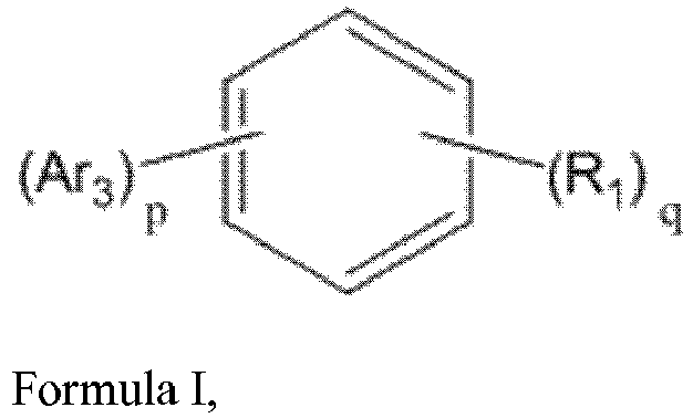
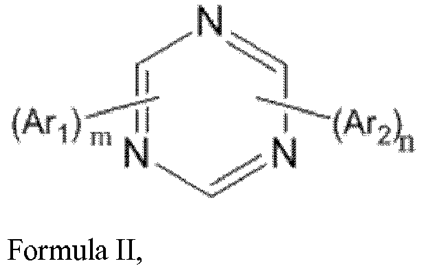
- thermally activated delayed fluorescence material provided by the present invention is a compound having the general structure of Formula I or Formula II:
- R 1 is a cyano
- p is 1, 2 or 3
- q is 1, 2 or 3
- m is 1 or 2
- n is 1 or 2
- Ar 1 is a phenyl substituted with one or more groups selected from C 1-6 alkyl, methoxy, ethoxy, or phenyl
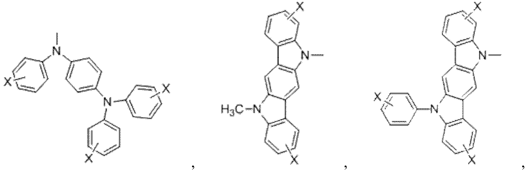
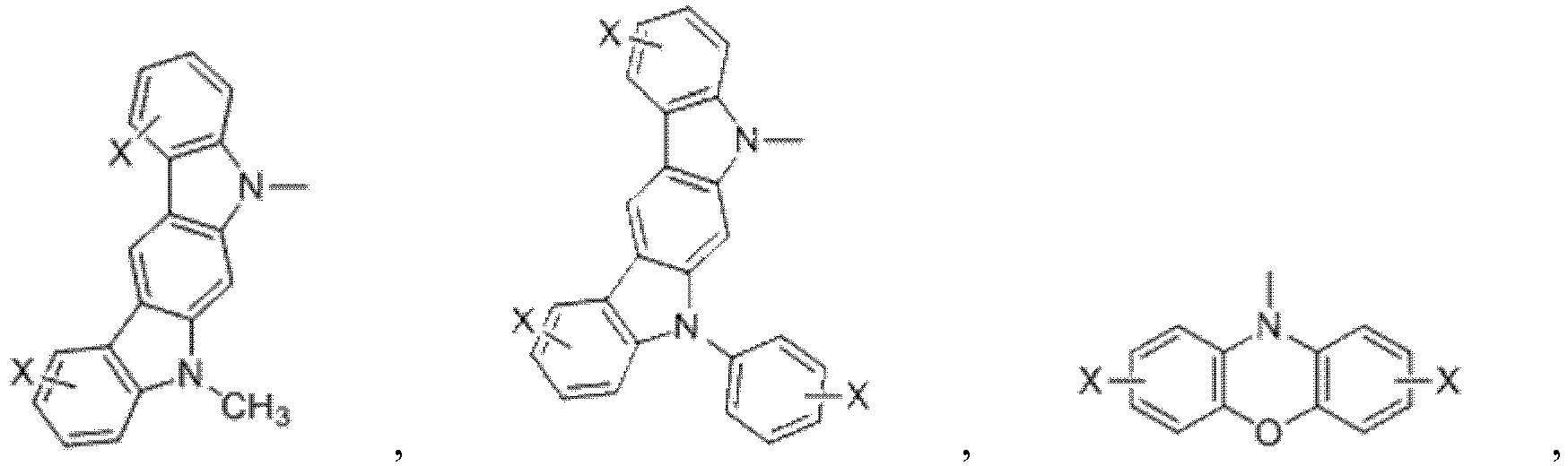
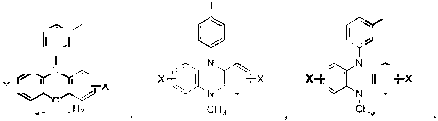
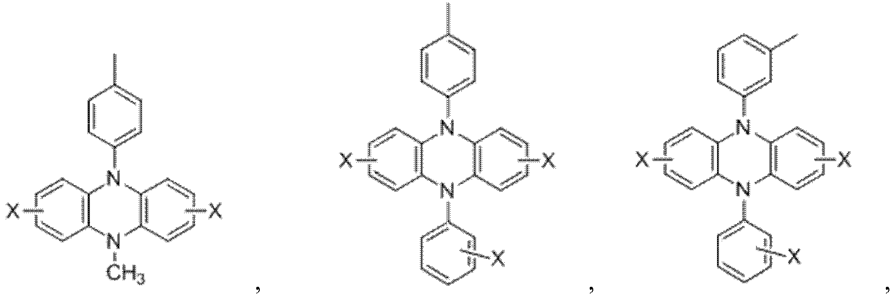
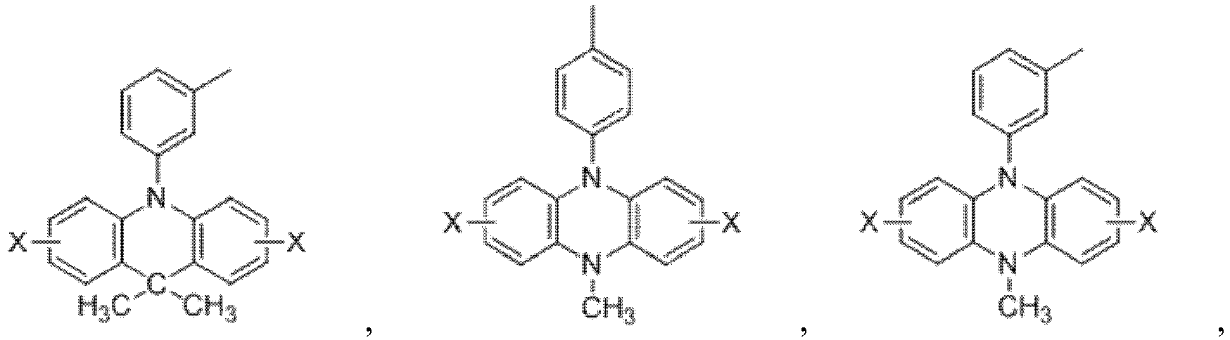
- Ar 2 and Ar 3 are selected from the following groups: and X is bromine or iodine.
- the thermally activated delayed fluorescence material is a compound having the following structure:
- the present invention also provides application of the thermally activated delayed fluorescence material as a host material or a luminescent dye of a luminescent layer of an organic electroluminescence device.
- the present invention further provides an organic electroluminescence device, comprising a luminescent layer, the luminescent layer comprises a host material and a luminescent dye doped in the host material, and the luminescent dye is the above thermally activated delayed fluorescence material.
- the luminescent dye accounts for 0.5 wt%-10 wt% of the luminescent layer, and more preferably 5 wt%.
- the organic electroluminescence device described above comprises an anode, a hole transport layer, a luminescent layer, an electron transport layer, and a cathode, which are successively deposited on a substrate and are laminated.
- a hole injection layer is further disposed between the anode and the hole transport layer.
- the present invention further provides an organic electroluminescence device, comprising a luminescent layer, the luminescent layer comprises a host material and a luminescent dye doped in the host material, and the host material is the above thermally activated delayed fluorescence material.
- the luminescent dye accounts for 1 wt%-10 wt% of the luminescent layer.
- the TADF material provided by the invention, by introducing heavy atoms such as bromine or iodine into molecules, the lifetime of the triplet state of the TADF material is reduced, and efficiency roll-off is reduced, thereby increasing the lifetime of the organic electroluminescence device.
- Fig. 1 is the schematic diagram of the structure of an organic electroluminescence device of the present invention.
- a thermally activated delayed fluorescence material provided in the invention is a compound having the general structure of Formula I or Formula II:
- R 1 is a cyano
- p is 1, 2 or 3
- q is 1, 2 or 3
- m is 1 or 2
- n is 1 or 2
- Ar 1 is a phenyl substituted with one or more groups selected from C 1-6 alkyl, methoxy, ethoxy, or phenyl
- Ar 2 and Ar 3 are selected from the following groups: and X is bromine or iodine.
- thermally activated delayed fluorescence material by introducing heavy atoms such as bromine or iodine into original TADF molecules, reverse intersystem crossing and intersystem crossing of the TADF material can be increased through the heavy atom effect, so that the lifetime of triplet excitons can be reduced, and ultimately the lifetime of a device can be increased.
- heavy atoms such as bromine or iodine
- the thermally activated delayed fluorescence material of the present invention can be used as a luminescent dye for a luminescent layer of an organic electroluminescence device.
- the organic electroluminescence device of the present invention comprises an anode 02, a hole injection layer 04, a hole transport layer 05, a luminescent layer 06, an electron transport layer 07 and a cathode 03, which are successively deposited on a substrate 01 and are laminated.
- the material of the luminescent layer 06 comprises a host material and a luminescent dye doped in the host material, and the luminescent material is a compound having the structure of Formula I or Formula II.
- the anode 02 may employ an inorganic material or an organic conductive polymer.
- the inorganic material may generally employ metal oxides such as indium tin oxide (ITO), zinc oxide (ZnO), and indium zinc oxide (IZO) or metals of high work functions such as gold, copper and silver, preferably ITO.
- the organic conductive polymer is preferably one of polythiophene/polyvinyl sodium benzenesulfonate (hereafter referred to as simply PEDOT/PSS) and polyaniline (hereafter referred to as simply PANI).
- PEDOT/PSS polythiophene/polyvinyl sodium benzenesulfonate
- PANI polyaniline
- the cathode 03 generally employs metals of low work function such as lithium, magnesium, calcium, strontium, aluminum and indium or their alloys with copper, gold or silver, or an electrode layer that is formed by the alternating of a metal and a metal fluoride.
- the cathode is preferably laminated LiF layer and Al layer (the LiF layer is on the outer side).
- the material of the hole transport layer 05 may be selected from lower molecular weight materials of the arylamine type and the branched polymer type, preferably NPB.
- the material of the electron transport layer 07 may employ an organic metal complex (such as Alq 3 , Gaq 3 , BAlq or Ga (Saph-q)) or other materials that are commonly used for electron transport layer, such as aromatic condensed ring type (such as pentacene and perylene) or o-phenanthroline type (such as Bphen and BCP) compounds.
- organic metal complex such as Alq 3 , Gaq 3 , BAlq or Ga (Saph-q)
- other materials that are commonly used for electron transport layer such as aromatic condensed ring type (such as pentacene and perylene) or o-phenanthroline type (such as Bphen and BCP) compounds.
- the organic electroluminescence device of the present invention may also be provided with the hole injection layer 04 between the anode 02 and the hole transport layer 05.
- the material of the hole injection layer 04 may employ, for example, 4,4',4"-tris(3-methylphenylaniline)triphenylamine doped F4TCNQ or copper phthalocyanine (CuPc), or may be a metal oxide, such as molybdenum oxide and rhenium oxide.
- the thicknesses of the layers may employ the conventional thicknesses of the layers in the art.
- the present invention further provides a preparation method of the organic electroluminescence device, which comprises successively depositing on the substrate 01 the anode 02, the hole injection layer 04, the hole transport layer 05, the luminescent layer 06, the electron transport layer 07 and the cathode 03, which are laminated, and packaging.
- the substrate may be glass or a flexible base sheet.
- the flexible base sheet may employ a polyester type or polyimide type compound material or a thin sheet metal.
- the laminating and the packaging may employ any suitable method that is known by a person skilled in the art. Comparative Example 1:
- This comparative example uses ITO (indium tin oxide) as the anode; NPB as the hole injection layer; TCTA as the hole transport layer; the luminescent layer uses CBP as the host material and DSA-Ph as the luminescent dye, and the mass percentage of the luminescent dye doped in the luminescent layer is 5 wt%; Bphen as the electron transport layer; LiF(5 nm)/Al as the cathode.
- ITO indium tin oxide
- NPB hole injection layer
- TCTA hole transport layer
- the luminescent layer uses CBP as the host material and DSA-Ph as the luminescent dye, and the mass percentage of the luminescent dye doped in the luminescent layer is 5 wt%
- Bphen as the electron transport layer
- LiF(5 nm)/Al as the cathode.
- the structures are as follows: ITO/NPB (40 nm)/TCTA(10 nm)/CBP: 5 wt% DSA-Ph (30 nm)/Bphen(40 nm)/LiF (5 nm)/Al
- the structure of this Comparative Example differs from that of Comparative Example 1 only in that the luminescent dye used in the luminescent layer is 2CzPN: ITO/NPB(40 nm)/TCTA(10 nm)/CBP: 5 wt% 2CzPN (30 nm)/Bphen(40 nm)/LiF (5 nm)/Al
- the structure of this embodiment differs from that of Comparative Example 1 only in that the luminescent dye used in the luminescent layer is compound 1-1 of the present invention: ITO/NPB(40 nm)/TCTA(10 nm)/CBP: 5 wt% compound 1-1 (30 nm)/Bphen(40 nm)/LiF (5 nm)/Al Serial number Luminance cd/m 2 Voltage V Current efficiency cd/A Lumen efficiency lm/W x(V) y(V) T 95 h Comparative Example 1 1000 6.7 10.2 4.8 0.16 0.35 51 Comparative Example 2 1000 4.5 11.38 6.25 0.12 0.32 24 Embodiment 1 1000 4.3 12.20 7.23 0.14 0.29 78
- the TADF material in Embodiment 1 due to the introduction of the heavy atoms, reverse intersystem crossing and intersystem crossing of the TADF material are increased through the heavy atom effect, so that the lifetime of triplet excitons is reduced, and ultimately the lifetime of the device is increased.
- Embodiments 2-5 differ from that of Embodiment 1 only in that the doping concentration of the luminescent dye compound 1-1 in the luminescent layer is different: ITO/NPB(40 nm)/TCTA(10 nm)/CBP: 0.5-10 wt% compound 1-1 (30 nm)/Bphen(40 nm)/LiF (5 nm)/Al Embodiments with different doping concentrations Serial number Doping concentration of dye wt% Luminance cd/m 2 Voltage V Current efficiency cd/A Lumen efficiency lm/W x(V) y(V) T 95 h Embodiments 1 5 1000 4.3 12.20 7.23 0.14 0.29 78 Embodiments 2 0.5 1000 3.2 10.35 6.02 0.14 0.29 55 Embodiments 3 1 1000 4.0 10.56 5.98 0.14 0.29 61 Embodiments 4 3 1000 4.2 11.32 6.99 0.14 0.29 69 Embodiments 5 10 1000 4.4 10.79 6.89 0.
- the increase of the concentration of the luminescent dye causes the current efficiency of the device to increase first and then decrease.
- the doping concentration is 5 wt%
- the current efficiency of the device is the highest, and the voltage of the device basically does not change, but the lifetime of the device is increased as the doping concentration of the luminescent dye increases.
- the OLED structure in this embodiment differs from Embodiment 1 only in that the luminescent layer is doped with a different compound having the structure of Formula I or Formula II as the luminescent dye: ITO/NPB(40 nm)/TCTA(10 nm)/CBP: 5 wt% (compound having the structure of Formula I or Formula II) (30 nm)/Bphen(40 nm)/LiF (5 nm)/Al Serial number TADF material used in luminescent layer Luminance cd/m 2 Voltage V Current efficiency cd/A Lumen efficiency lm/W x(V) y(V) T 95 h OLED1 1-2 1000 5.4 13.26 8.98 0.13 0.22 59 OLED2 1-3 1000 4.9 11.38 6.57 0.15 0.22 62 OLED3 1-4 1000 5.0 29.32 19.25 0.56 0.50 132 OLED4 1-5 1000 4.8 30.21 20.36 0.50, 0.48 111 OLED5 2-1 1000 4.9 31.
- Embodiment 7 Embodiment 8 and Embodiment 9 with different doping concentrations that the electrical property of the device increases first and then decreases with an increase in the doping concentration of the luminescent dye, and is optimize at the doping concentration of 5 wt%, but the lifetime of the device increases as the doping concentration of the dye increases.
- the lifetime of the device protected by the present invention with the thermally activated delayed fluorescence material containing the heavy bromine atoms serving as the host is longer than that of a conventional device with CBP as a host (Comparative Example 3), and comparing with a device with a thermally activated sensitized fluorescent material of the same structure but without heavy atoms serving as a host (Comparative Example 4), the electrical property does not change much, but the lifetime of the device of Example 7 is longer than that of the device of Comparative Example 4, because the reverse intersystem crossing coefficient of the TADF material is increased through the heavy atom effect, so that the lifetime of triplet excitons is reduced, and ultimately the lifetime of the device is increased.
Landscapes
- Chemical & Material Sciences (AREA)
- Organic Chemistry (AREA)
- Engineering & Computer Science (AREA)
- Materials Engineering (AREA)
- Physics & Mathematics (AREA)
- Spectroscopy & Molecular Physics (AREA)
- Optics & Photonics (AREA)
- Electroluminescent Light Sources (AREA)
Abstract
Ar1 is a phenyl substituted with one or more groups selected from C1-6 alkyl, methoxy, ethoxy, or phenyl,
Ar2 and Ar3 are selected from the following groups:





Description
- The present invention belongs to the field of materials, and particularly relates to a thermally activated delayed fluorescence material and application thereof in an organic electroluminescence device.
- In the electroluminescence process of an organic electroluminescence device, luminescence occurs mainly due to the electronic transition of an organic luminescent material from an excited state to a ground state. At room temperature, luminescence generated by the electronic transition from a triplet excited state back to the ground state is extremely weak, most of the energy is lost in the form of heat, and luminescence is mainly generated by the electronic transition from a singlet excitation state to the ground state, and is called electroluminescence. Since the probability of the triplet excited state is three times that of the singlet excitation state, the equivalent of 75% of the energy is not used for luminescence. Making full use of the energy will effectively improve the luminescence efficiency of the organic electroluminescence device.
- In order to make full use of the energy of the triplet excited state of a host material of a luminescent layer, various methods have been proposed. For example, by researching and developing an efficient phosphorescence doping dye and doping the phosphorescence doping dye into the host material, the triplet energy of the host material can be effectively transmitted to the phosphorescence doping dye, and then the phosphorescence doping dye generates phosphorescence, thereby allowing the energy of the triplet excited state of the host material of the luminescent layer to be effectively used. The organic electroluminescence device obtained by this method has high efficiency, but material synthesis requires precious metals such as ruthenium and platinum which are expensive. Another method is to utilize the intersystem crossing property of lanthanide compounds, namely intramolecular energy transfer, to transfer the triplet energy of the host material of the luminescent layer to the 4f energy level of lanthanide metal ions, and then luminescence and the like are achieved, but current devices are inefficient.
- Thermally activated delayed fluorescence (TADF) is a quite popular scheme utilizing triplet exciton energy at present. For example, Adachi reported in his article a thermally activated delayed fluorescence material which has a small difference (ΔEST) between the triplet energy level (T1) and the singlet energy level (S1), in this way, triplet energy can be transmitted to the singlet energy level, and light is emitted through fluorescent radiation. Patent
CN 102709485 A mentions that device efficiency is improved by doping a fluorescent dye in a thermal delay fluorescent host. In order to further improve energy transmission recombination efficiency, in the article "High-efficiency organic light-emitting diodes with fluorescent emitters" by Adachi et al. in Nature communications 2014, a wide-band-gap host doped TADF material is proposed as an auxiliary dye solution. However, in the process of charge recombination, part of the energy is directly compounded on a host, the host transmits the singlet energy to a dye, and the other part is compounded on an auxiliary dye. The structure reported in the article can not fully and effectively utilize the energy directly compounded on the host. At the same time, an ordinary host material is used, a band gap is wide, and required driving voltage is high. - However, the current TADF material has a short lifetime, and one of the reasons is that the lifetime of the triplet state is too long, and exciton quenching can be caused easily due to processes such as TPA. Therefore, the lifetime of a TADF device can be effectively increased by reducing the lifetime of triplet excitons.
- The technical problem to be solved by the present invention is that a TADF material in the prior art has a short lifetime.
- In order to solve the above technical problem, the present invention provides a novel TADF material. By introducing heavy atoms such as bromine or iodine into original TADF molecules, reverse intersystem crossing and intersystem crossing of the TADF material can be increased through the heavy atom effect, so that the lifetime of triplet excitons can be reduced, and ultimately the lifetime of a device can be increased.
- The thermally activated delayed fluorescence material provided by the present invention is a compound having the general structure of Formula I or Formula II:


- In Formula I and Formula II, R1 is a cyano, p is 1, 2 or 3, q is 1, 2 or 3, m is 1 or 2, n is 1 or 2,
Ar1 is a phenyl substituted with one or more groups selected from C1-6 alkyl, methoxy, ethoxy, or phenyl,
Ar2 and Ar3 are selected from the following groups:




- Preferably, the thermally activated delayed fluorescence material is a compound having the following structure:


- The present invention also provides application of the thermally activated delayed fluorescence material as a host material or a luminescent dye of a luminescent layer of an organic electroluminescence device.
- The present invention further provides an organic electroluminescence device, comprising a luminescent layer, the luminescent layer comprises a host material and a luminescent dye doped in the host material, and the luminescent dye is the above thermally activated delayed fluorescence material. Preferably, the luminescent dye accounts for 0.5 wt%-10 wt% of the luminescent layer, and more preferably 5 wt%.
- As a preferred technical solution, the organic electroluminescence device described above comprises an anode, a hole transport layer, a luminescent layer, an electron transport layer, and a cathode, which are successively deposited on a substrate and are laminated.
- Preferably, a hole injection layer is further disposed between the anode and the hole transport layer.
- The present invention further provides an organic electroluminescence device, comprising a luminescent layer, the luminescent layer comprises a host material and a luminescent dye doped in the host material, and the host material is the above thermally activated delayed fluorescence material.
- Preferably, the luminescent dye accounts for 1 wt%-10 wt% of the luminescent layer.
- According to the TADF material provided by the invention, by introducing heavy atoms such as bromine or iodine into molecules, the lifetime of the triplet state of the TADF material is reduced, and efficiency roll-off is reduced, thereby increasing the lifetime of the organic electroluminescence device.
-
Fig. 1 is the schematic diagram of the structure of an organic electroluminescence device of the present invention. - The present invention will be further illustrated below by referring to the drawings and the special examples, to enable a person skilled in the art to better understand and implement the present invention, but the examples are not taken as limiting the present invention.
- A thermally activated delayed fluorescence material provided in the invention is a compound having the general structure of Formula I or Formula II:


- In Formula I and Formula II, R1 is a cyano, p is 1, 2 or 3, q is 1, 2 or 3, m is 1 or 2, n is 1 or 2,
Ar1 is a phenyl substituted with one or more groups selected from C1-6 alkyl, methoxy, ethoxy, or phenyl,
Ar2 and Ar3 are selected from the following groups:


- According to the thermally activated delayed fluorescence material, by introducing heavy atoms such as bromine or iodine into original TADF molecules, reverse intersystem crossing and intersystem crossing of the TADF material can be increased through the heavy atom effect, so that the lifetime of triplet excitons can be reduced, and ultimately the lifetime of a device can be increased.
- Specifically, the thermally activated delayed fluorescence material of the present invention is compounds having the following structures, and properties and preparation methods of the compounds are as follows:

- Synthesis of the compound having the structure represented by Formula (1-1): in the nitrogen range, 3-bromocarbazole (5 mmol) is dissolved in 2 mL of anhydrous THF, then sodium hydride (5 mmol) is added, and the mixture is stirred at room temperature for 30 minutes; subsequently, 1,2-dicyano-4,5-difluorobenzene (1 mmol) is added to a reaction flask and stirring is continued for 1 hour; finally, 2 mL of cold water is added to the mixture to quench the reaction. After the mixture is cooled to room temperature, a product of Formula (1-1) is purified by vacuum filtration followed by column chromatography, and the product is dried in vacuum. Yield: 75%.
- Molecular weight obtained through mass spectrometry: 615.97.
- Relative molecular mass percentage of each element obtained through elemental analysis: C: 62.36; H: 2.62; N: 9.09; Br: 25.93.

- Synthesis of the compound having the structure represented by Formula (1-2): in the nitrogen range, 3-bromophenothiazine (10 mmol) is dissolved in 4 mL of anhydrous THF, then sodium hydride (10 mmol) is added, and the mixture is stirred at room temperature for 30 minutes; subsequently, 2,3,5,6-tetrafluoro nitrile benzene (1 mmol) is added to a reaction flask and stirring is continued for 1 hour; finally, 2 mL of cold water is added to the mixture to quench the reaction.
- After the mixture is cooled to room temperature, a product of Formula (1-2) is purified by vacuum filtration followed by column chromatography, and the product is dried in vacuum. Yield: 62%.
- Molecular weight obtained through mass spectrometry: 1206.80.
- Relative molecular mass percentage of each element obtained through elemental analysis: C: 54.70; H: 2.42; N: 5.80; S: 10.62; Br: 26.46.

- Synthesis of the compound having the structure represented by Formula (1-3): the reactant 3-bromophenothiazine is replaced with 3-bromophenoxazine, the compound having the structure represented by Formula (1-3) is obtained by a synthesis method which is the same as that of Formula (1-2), and yield is 59%.
- Molecular weight obtained through mass spectrometry: 1142.89.
- Relative molecular mass percentage of each element obtained through elemental analysis: C: 57.77; H: 2.56; N: 6.12; O: 5.60; Br: 27.95.

- Synthesis of the compound having the structure represented by Formula (1-4): the reactant 3-bromophenothiazine is replaced with 9-p-iodobenzene phenazine, the compound having the structure represented by Formula (1-4) is obtained by a synthesis method which is the same as that of Formula (1-2), and yield is 55%.
- Molecular weight obtained through mass spectrometry: 1631.03.
- Relative molecular mass percentage of each element obtained through elemental analysis: C: 58.14; H: 3.03; N: 7.72; I: 31.11.

- Synthesis of the compound having the structure represented by Formula (1-5): in the nitrogen range, (1,1'-p-dibromobenzene) p-aminobenzene (15 mmol) is dissolved in 6 mL of anhydrous THF, then sodium hydride (15 mmol) is added, and the mixture is stirred at room temperature for 30 minutes; subsequently, 2,4,6-tetrafluoro-1,3,5-tricyanobenzene (1 mmol) is added to a reaction flask and stirring is continued for 1 hour; finally, 2 mL of cold water is added to the mixture to quench the reaction. After the mixture is cooled to room temperature, a product of Formula (1-5) is purified by vacuum filtration followed by column chromatography, and the product is dried in vacuum. Yield: 31%.
- Molecular weight obtained through mass spectrometry: 1355.80.
- Relative molecular mass percentage of each element obtained through elemental analysis: C: 55.78; H: 2.68; N: 6.20; Br: 35.34.

- Synthesis of the compound having the structure represented by Formula (2-1): in the nitrogen range, 3,6-dibromocarbazolylbenzene (10 mmol) is dissolved in 4 mL of anhydrous THF, then sodium hydride (15 mmol) is added, and the mixture is stirred at room temperature for 30 minutes; subsequently, 1-phenyl-1,3,5-triazine (1 mmol) is added to a reaction flask and stirring is continued for 1 hour; finally, 2 mL of cold water is added to the mixture to quench the reaction.
- After the mixture is cooled to room temperature, a product of Formula (2-1) is purified by vacuum filtration followed by column chromatography, and the product is dried in vacuum. Yield: 49%.
- Molecular weight obtained through mass spectrometry: 955.33.
- Relative molecular mass percentage of each element obtained through elemental analysis: C: 56.58; H: 2.64; N: 7.33; Br: 33.46.

- Synthesis of the compound having the structure represented by Formula (2-2): in the nitrogen range, p-bromobenzene (5 mmol) is dissolved in 4 mL of anhydrous THF, then sodium hydride (5 mmol) is added, and the mixture is stirred at room temperature for 30 minutes; subsequently, 2,4-bis(3-bicarbazole)-6-fluoro-1,3,5-triazine (1 mmol) is added to a reaction flask and stirring is continued for 1 hour; finally, 2 mL of cold water is added to the mixture to quench the reaction.
- After the mixture is cooled to room temperature, a product of Formula (2-2) is purified by vacuum filtration followed by column chromatography, and the product is dried in vacuum. Yield: 53%.
- Molecular weight obtained through mass spectrometry: 895.21.
- Relative molecular mass percentage of each element obtained through elemental analysis: C: 76.34; H: 3.82; N: 10.93; Br: 8.91.

- Synthesis of the compound having the structure represented by Formula (2-3): in the nitrogen range, p-iodobenzene (10 mmol) is dissolved in 4 mL of anhydrous THF, then sodium hydride (10 mmol) is added, and the mixture is stirred at room temperature for 30 minutes; subsequently, 2,4-bis(3-bicarbazole)-1,3,5-triazine (1 mmol) is added to a reaction flask and stirring is continued for 1 hour; finally, 2 mL of cold water is added to the mixture to quench the reaction. After the mixture is cooled to room temperature, a product of Formula (2-3) is purified by vacuum filtration followed by column chromatography, and the product is dried in vacuum. Yield: 53%.
- Molecular weight obtained through mass spectrometry: 891.04.
- Relative molecular mass percentage of each element obtained through elemental analysis: C: 60.62; H: 3.05; N: 7.86; I: 28.47.

- Synthesis of the compound having the structure represented by Formula (2-4): in the nitrogen range, p-diiodobenzene-4,4'-diaminobenzenes (5 mmol) is dissolved in 4 mL of anhydrous THF, then sodium hydride (5 mmol) is added, and the mixture is stirred at room temperature for 30 minutes; subsequently, 4-fluoro-2,6-phenyl-1,3,5-triazine (1 mmol) is added to a reaction flask and stirring is continued for 1 hour; finally, 2 mL of cold water is added to the mixture to quench the reaction. After the mixture is cooled to room temperature, a product of Formula (2-4) is purified by vacuum filtration followed by column chromatography, and the product is dried in vacuum. Yield: 40%.
- Molecular weight obtained through mass spectrometry: 1313.93.
- Relative molecular mass percentage of each element obtained through elemental analysis: C: 52.08; H: 2.91; N: 6.39; I: 38.61.
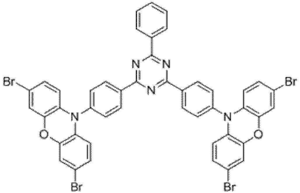
- Synthesis of the compound having the structure represented by Formula (2-5): the reactant 3,6-dibromocarbazolylbenzene is replaced with 3,7-dibromophenoxazinebenzene, the compound having the structure represented by Formula (2-5) is obtained by a synthesis method which is the same as that of Formula (2-1), and yield is 61%.
- Molecular weight obtained through mass spectrometry: 986.87.
- Relative molecular mass percentage of each element obtained through elemental analysis: C: 54.74; H: 2.55; N: 7.09; O: 3.24; Br: 32.37.

- Synthesis of the compound having the structure represented by Formula (2-6): the reactant 3,6-dibromocarbazolylbenzene is replaced with 3,7-dibromophenoxazine-m-benzene, the compound having the structure represented by Formula (2-6) is obtained by a synthesis method which is the same as that of Formula (2-1), and yield is 61%.
- Molecular weight obtained through mass spectrometry: 1174.82.
- Relative molecular mass percentage of each element obtained through elemental analysis: C: 45.99; H: 2.14; N: 5.96; O: 2.72; I: 43.19.
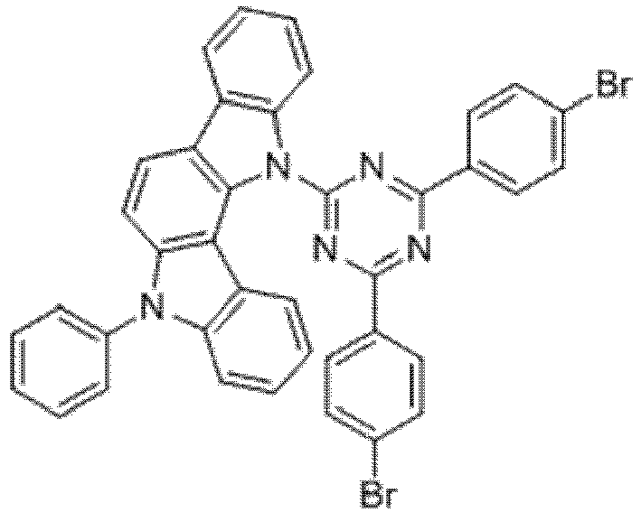
- Synthesis of the compound having the structure represented by Formula (2-7): in the nitrogen range, dibromo-benzene (10 mmol) is dissolved in 4 mL of anhydrous THF, then sodium hydride (10 mmol) is added, and the mixture is stirred at room temperature for 30 minutes; subsequently, 2,4-difluoro-6-(11-phenyl-11,12-dihydroindolo[3,2b]carbazolyl)-2,6-phenyl-1,3,5-triazine (1 mmol) is added to a reaction flask and stirring is continued for 1 hour; finally, 2 mL of cold water is added to the mixture to quench the reaction. After the mixture is cooled to room temperature, a product of Formula (2-7) is purified by vacuum filtration followed by column chromatography, and the product is dried in vacuum. Yield: 34%.
- Molecular weight obtained through mass spectrometry: 721.03.
- Relative molecular mass percentage of each element obtained through elemental analysis: C: 64.93; H: 3.21; N: 9.71; Br: 22.15.

- Synthesis of the compound having the structure represented by Formula (2-8): in the nitrogen range, 6-phenyl-2,9-diiodo-indolo[2,3a]carbazole (10 mmol) is dissolved in 4 mL of anhydrous THF, then sodium hydride (10 mmol) is added, and the mixture is stirred at room temperature for 30 minutes; subsequently, 6-fluoro-2,4-diphenyl-1,3,5-triazine (1 mmol) is added to a reaction flask and stirring is continued for 1 hour; finally, 2 mL of cold water is added to the mixture to quench the reaction. After the mixture is cooled to room temperature, a product of Formula (2-8) is purified by vacuum filtration followed by column chromatography, and the product is dried in vacuum. Yield: 31%.
- Molecular weight obtained through mass spectrometry: 815.44.
- Relative molecular mass percentage of each element obtained through elemental analysis: C: 57.44; H: 2.84; N: 8.59; I: 31.13.

- Synthesis of the compound having the structure represented by Formula (2-9): in the nitrogen range, 11-p-bromophenyl-indolo[2,3a]carbazole (7 mmol) is dissolved in 4 mL of anhydrous THF, then sodium hydride (10 mmol) is added, and the mixture is stirred at room temperature for 30 minutes; subsequently, 6-fluoro-2,4-p-dibromophenyl-1,3,5-triazine (1 mmol) is added to a reaction flask and stirring is continued for 1 hour; finally, 2 mL of cold water is added to the mixture to quench the reaction. After the mixture is cooled to room temperature, a product of Formula (2-9) is purified by vacuum filtration followed by column chromatography, and the product is dried in vacuum. Yield: 36%.
- Molecular weight obtained through mass spectrometry: 800.34.
- Relative molecular mass percentage of each element obtained through elemental analysis: C: 58.53; H: 2.77; N: 8.75; Br: 29.95.
- The thermally activated delayed fluorescence material of the present invention can be used as a luminescent dye for a luminescent layer of an organic electroluminescence device.
- As shown by
Fig. 1 , the organic electroluminescence device of the present invention comprises ananode 02, ahole injection layer 04, ahole transport layer 05, aluminescent layer 06, anelectron transport layer 07 and acathode 03, which are successively deposited on asubstrate 01 and are laminated. - The material of the
luminescent layer 06 comprises a host material and a luminescent dye doped in the host material, and
the luminescent material is a compound having the structure of Formula I or Formula II. - The embodiments of the organic luminescence display device of the present invention: the
anode 02 may employ an inorganic material or an organic conductive polymer. The inorganic material may generally employ metal oxides such as indium tin oxide (ITO), zinc oxide (ZnO), and indium zinc oxide (IZO) or metals of high work functions such as gold, copper and silver, preferably ITO. - The organic conductive polymer is preferably one of polythiophene/polyvinyl sodium benzenesulfonate (hereafter referred to as simply PEDOT/PSS) and polyaniline (hereafter referred to as simply PANI).
- The
cathode 03 generally employs metals of low work function such as lithium, magnesium, calcium, strontium, aluminum and indium or their alloys with copper, gold or silver, or an electrode layer that is formed by the alternating of a metal and a metal fluoride. In the present invention the cathode is preferably laminated LiF layer and Al layer (the LiF layer is on the outer side). - The material of the
hole transport layer 05 may be selected from lower molecular weight materials of the arylamine type and the branched polymer type, preferably NPB. - The material of the
electron transport layer 07 may employ an organic metal complex (such as Alq3, Gaq3, BAlq or Ga (Saph-q)) or other materials that are commonly used for electron transport layer, such as aromatic condensed ring type (such as pentacene and perylene) or o-phenanthroline type (such as Bphen and BCP) compounds. - The organic electroluminescence device of the present invention may also be provided with the
hole injection layer 04 between theanode 02 and thehole transport layer 05. The material of thehole injection layer 04 may employ, for example, 4,4',4"-tris(3-methylphenylaniline)triphenylamine doped F4TCNQ or copper phthalocyanine (CuPc), or may be a metal oxide, such as molybdenum oxide and rhenium oxide. - The thicknesses of the layers may employ the conventional thicknesses of the layers in the art.
- The present invention further provides a preparation method of the organic electroluminescence device, which comprises successively depositing on the
substrate 01 theanode 02, thehole injection layer 04, thehole transport layer 05, theluminescent layer 06, theelectron transport layer 07 and thecathode 03, which are laminated, and packaging. - The substrate may be glass or a flexible base sheet. The flexible base sheet may employ a polyester type or polyimide type compound material or a thin sheet metal. The laminating and the packaging may employ any suitable method that is known by a person skilled in the art. Comparative Example 1:
- This comparative example uses ITO (indium tin oxide) as the anode; NPB as the hole injection layer; TCTA as the hole transport layer; the luminescent layer uses CBP as the host material and DSA-Ph as the luminescent dye, and the mass percentage of the luminescent dye doped in the luminescent layer is 5 wt%; Bphen as the electron transport layer; LiF(5 nm)/Al as the cathode.
- The structures are as follows:
ITO/NPB (40 nm)/TCTA(10 nm)/CBP: 5 wt% DSA-Ph (30 nm)/Bphen(40 nm)/LiF (5 nm)/Al


- The structure of this Comparative Example differs from that of Comparative Example 1 only in that the luminescent dye used in the luminescent layer is 2CzPN:
ITO/NPB(40 nm)/TCTA(10 nm)/CBP: 5 wt% 2CzPN (30 nm)/Bphen(40 nm)/LiF (5 nm)/Al
- The structure of this embodiment differs from that of Comparative Example 1 only in that the luminescent dye used in the luminescent layer is compound 1-1 of the present invention:

Serial number Luminance cd/m2 Voltage V Current efficiency cd/A Lumen efficiency lm/W x(V) y(V) T95 h Comparative Example 1 1000 6.7 10.2 4.8 0.16 0.35 51 Comparative Example 2 1000 4.5 11.38 6.25 0.12 0.32 24 Embodiment 1 1000 4.3 12.20 7.23 0.14 0.29 78 - According to the TADF material in Embodiment 1, due to the introduction of the heavy atoms, reverse intersystem crossing and intersystem crossing of the TADF material are increased through the heavy atom effect, so that the lifetime of triplet excitons is reduced, and ultimately the lifetime of the device is increased.
- The structures of Embodiments 2-5 differ from that of Embodiment 1 only in that the doping concentration of the luminescent dye compound 1-1 in the luminescent layer is different: ITO/NPB(40 nm)/TCTA(10 nm)/CBP: 0.5-10 wt% compound 1-1 (30 nm)/Bphen(40 nm)/LiF (5 nm)/Al
Embodiments with different doping concentrations Serial number Doping concentration of dye wt% Luminance cd/m2 Voltage V Current efficiency cd/A Lumen efficiency lm/W x(V) y(V) T95 h Embodiments 1 5 1000 4.3 12.20 7.23 0.14 0.29 78 Embodiments 2 0.5 1000 3.2 10.35 6.02 0.14 0.29 55 Embodiments 3 1 1000 4.0 10.56 5.98 0.14 0.29 61 Embodiments 4 3 1000 4.2 11.32 6.99 0.14 0.29 69 Embodiments 5 10 1000 4.4 10.79 6.89 0.14 0.29 79 - From the above table, it can be seen that the increase of the concentration of the luminescent dye causes the current efficiency of the device to increase first and then decrease. When the doping concentration is 5 wt%, the current efficiency of the device is the highest, and the voltage of the device basically does not change, but the lifetime of the device is increased as the doping concentration of the luminescent dye increases.
- The OLED structure in this embodiment differs from Embodiment 1 only in that the luminescent layer is doped with a different compound having the structure of Formula I or Formula II as the luminescent dye:
ITO/NPB(40 nm)/TCTA(10 nm)/CBP: 5 wt% (compound having the structure of Formula I or Formula II) (30 nm)/Bphen(40 nm)/LiF (5 nm)/AlSerial number TADF material used in luminescent layer Luminance cd/m2 Voltage V Current efficiency cd/A Lumen efficiency lm/W x(V) y(V) T95 h OLED1 1-2 1000 5.4 13.26 8.98 0.13 0.22 59 OLED2 1-3 1000 4.9 11.38 6.57 0.15 0.22 62 OLED3 1-4 1000 5.0 29.32 19.25 0.56 0.50 132 OLED4 1-5 1000 4.8 30.21 20.36 0.50, 0.48 111 OLED5 2-1 1000 4.9 31.15 22.89 0.51, 0.49 110 OLED6 2-2 1000 4.5 38.56 24.25 0.49, 0.45 75 OLED7 2-3 1000 5.0 28.78 20.45 0.55, 0.50 121 OLED8 2-4 1000 5.5 6.00 5.21 0.20, 0.35 59 OLED9 2-5 1000 4.8 18.26 15.23 0.22 0.40 78 OLED10 2-6 1000 5.5 8.75 17.41 0.20 0.41 62 OLED11 2-7 1000 5.4 16.62 16.66 0.16 0.21 41 OLED12 2-8 1000 5.3 17.12 15.91 0.17 0.21 50 OLED13 2-9 1000 5.2 18.22 15.02 0.17, 0.22 52 - From the above table, it can be seen that the lifetime of the thermally activated delayed fluorescence material containing the heavy atoms of bromine or iodine, as well as the lifetime of the device protected by the invention are both increased, the reason is that reverse intersystem crossing and intersystem crossing of the TADF material are increased through the heavy atom effect, so that the lifetime of triplet excitons is reduced, and ultimately the lifetime of the device is increased.
- The difference between the OLED structure in the embodiments and Embodiment 1 lies in that the host material in the luminescent layer is compound 2-2, and the luminescent dye is Ir(ppy)3. The doping concentration (weight percentage in the luminescent layer) of Ir(ppy)3 is 1-10 wt%. ITO/NPB(40 nm)/TCTA(10 nm)/compound 2-2: 1-10 wt% Ir(ppy)3 (30 nm)/Bphen(40 nm)/LiF (5 nm)/Al
- The difference between the structure of this Comparative Example and Embodiments 7-9 is only that the host material used for the luminescent layer is CBP:
ITO/NPB(40 nm)/TCTA(10 nm)/CBP: 5 wt% Ir(ppy)3 (30 nm)/Bphen(40 nm)/LiF (5 nm)/Al - The difference between the structure of this Comparative Example and Embodiments 7-9 is only that the host material used for the luminescent layer is CC2TA:


Serial number Doping concentration of dye wt% Luminance cd/m2 Voltage V Current efficiency cd/A Lumen efficiency lm/W x(V) y(V) T95 h (at 10000 cd/m2) Embodiments 7 5 wt% 1000 3.4 67 91 0.27 0.63 274 Embodiments 8 1 wt% 1000 3.0 60 86 0.26 0.63 260 Embodiments 9 10 wt% 1000 4.2 59 82 0.27 0.64 280 Comparative Example 3 5 wt% 1000 5.4 45 62 0.26 0.63 242 Comparative Example 4 5 wt% 1000 3.9 62 90 0.26 0.62 266 - From the above table, it can be seen by comparing Embodiment 7, Embodiment 8 and Embodiment 9 with different doping concentrations that the electrical property of the device increases first and then decreases with an increase in the doping concentration of the luminescent dye, and is optimize at the doping concentration of 5 wt%, but the lifetime of the device increases as the doping concentration of the dye increases. In addition, the lifetime of the device protected by the present invention with the thermally activated delayed fluorescence material containing the heavy bromine atoms serving as the host is longer than that of a conventional device with CBP as a host (Comparative Example 3), and comparing with a device with a thermally activated sensitized fluorescent material of the same structure but without heavy atoms serving as a host (Comparative Example 4), the electrical property does not change much, but the lifetime of the device of Example 7 is longer than that of the device of Comparative Example 4, because the reverse intersystem crossing coefficient of the TADF material is increased through the heavy atom effect, so that the lifetime of triplet excitons is reduced, and ultimately the lifetime of the device is increased.
- The above-described embodiments are merely preferred embodiments for fully explaining the present invention, and the scope of protection of the present invention is not limited thereto. The equivalent substitutions or alternations that are made by a person skilled in the art on the basis of the present invention all fall within the protection scope of the present invention. The protection scope of the present invention is limited by the claims.
Claims (10)
- A thermally activated delayed fluorescence material, characterized in that the thermally activated delayed fluorescence material is a compound having the general structure of Formula I or Formula II:
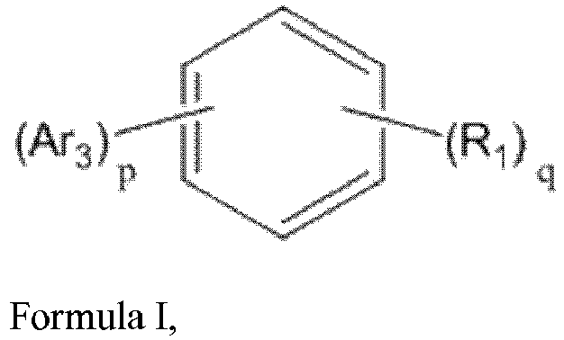

Ar1 is a phenyl substituted with one or more groups selected from C1-6alkyl, methoxy, ethoxy, or phenyl,
Ar2 and Ar3 are selected from the following groups:


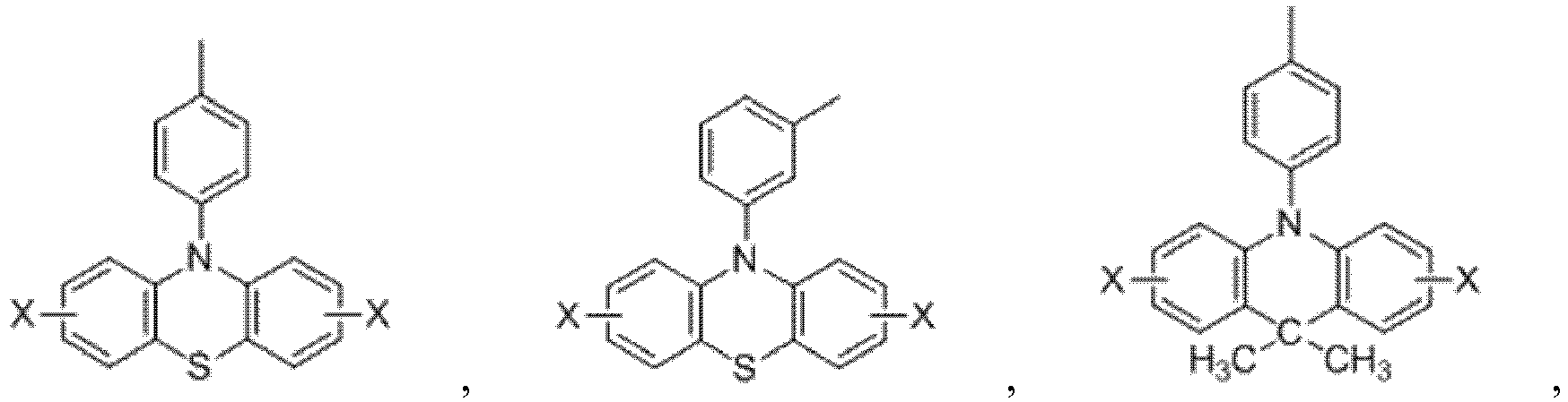


- The thermally activated delayed fluorescence material according to claim 1, characterized in that the thermally activated delayed fluorescence material is a compound having the following structure:


- Application of the thermally activated delayed fluorescence material according to claim 1 or 2, characterized in that the thermally activated delayed fluorescence material is used as a host material or a luminescent dye of a luminescent layer of an organic electroluminescence device.
- An organic electroluminescence device, comprising a luminescent layer, characterized in that the luminescent layer comprises a host material and a luminescent dye doped in the host material, and the luminescent dye is the thermally activated delayed fluorescence material according to claim 1 or 2.
- The organic electroluminescence device according to claim 4, characterized in that the luminescent dye accounts for 0.5 wt%-10 wt% of the luminescent layer.
- The organic electroluminescence device according to claim 5, characterized in that the luminescent dye accounts for 5 wt% of the luminescent layer.
- The organic electroluminescence device according to claim 4, characterized in that the organic electroluminescence device comprises an anode, a hole transport layer, a luminescent layer, an electron transport layer, and a cathode, which are successively deposited on a substrate and are laminated.
- The organic electroluminescence device according to claim 7, characterized in that a hole injection layer is further disposed between the anode and the hole transport layer.
- An organic electroluminescence device, comprising a luminescent layer, characterized in that the luminescent layer comprises a host material and a luminescent dye doped in the host material, and the host material is the thermally activated delayed fluorescence material according to claim 1 or 2.
- The organic electroluminescence device according to claim 9, characterized in that the luminescent dye accounts for 1 wt%-10 wt% of the luminescent layer.
Applications Claiming Priority (2)
| Application Number | Priority Date | Filing Date | Title |
|---|---|---|---|
| CN201510957493.2A CN106892857B (en) | 2015-12-18 | 2015-12-18 | Thermally Activated Delayed Fluorescent Materials and Their Applications in Organic Electroluminescent Devices |
| PCT/CN2016/107913 WO2017101675A1 (en) | 2015-12-18 | 2016-11-30 | Thermally activated delayed fluorescence material and use thereof in organic electroluminescent device |
Publications (3)
| Publication Number | Publication Date |
|---|---|
| EP3369728A1 true EP3369728A1 (en) | 2018-09-05 |
| EP3369728A4 EP3369728A4 (en) | 2019-02-13 |
| EP3369728B1 EP3369728B1 (en) | 2020-12-23 |
Family
ID=59055803
Family Applications (1)
| Application Number | Title | Priority Date | Filing Date |
|---|---|---|---|
| EP16874732.7A Active EP3369728B1 (en) | 2015-12-18 | 2016-11-30 | Thermally activated delayed fluorescence material and application thereof in organic electroluminescent device |
Country Status (7)
| Country | Link |
|---|---|
| US (1) | US10770661B2 (en) |
| EP (1) | EP3369728B1 (en) |
| JP (1) | JP2019501986A (en) |
| KR (1) | KR20180063264A (en) |
| CN (1) | CN106892857B (en) |
| TW (1) | TWI617648B (en) |
| WO (1) | WO2017101675A1 (en) |
Cited By (1)
| Publication number | Priority date | Publication date | Assignee | Title |
|---|---|---|---|---|
| US11569452B2 (en) | 2018-09-19 | 2023-01-31 | Samsung Electronics Co., Ltd. | Organic light-emitting device |
Families Citing this family (28)
| Publication number | Priority date | Publication date | Assignee | Title |
|---|---|---|---|---|
| JP6829547B2 (en) | 2015-12-28 | 2021-02-10 | 株式会社Kyulux | Compounds, light emitting materials and organic light emitting devices |
| US10892425B1 (en) | 2017-03-03 | 2021-01-12 | Kyulux, Inc. | Composition of matter for use in organic light-emitting diodes |
| US11283027B1 (en) | 2017-03-03 | 2022-03-22 | Kyulux, Inc. | Composition of matter for use in organic light-emitting diodes |
| US10547014B2 (en) | 2017-06-23 | 2020-01-28 | Kyulux, Inc. | Composition of matter for use in organic light-emitting diodes |
| KR102577834B1 (en) | 2017-06-23 | 2023-09-12 | 가부시키가이샤 큐럭스 | Compositions used in organic light emitting diodes |
| CN109206413A (en) * | 2017-07-07 | 2019-01-15 | 固安鼎材科技有限公司 | One kind is containing heavy-atom compounds, its application and organic electroluminescence device |
| US11069860B2 (en) | 2017-08-21 | 2021-07-20 | Kyulux, Inc. | Composition of matter for use in organic light-emitting diodes |
| US11444250B2 (en) | 2017-12-05 | 2022-09-13 | Kyulux, Inc. | Composition of matter for use in organic light-emitting diodes |
| CN108048077B (en) * | 2017-12-11 | 2019-04-30 | 中节能万润股份有限公司 | A kind of thermal activation delayed fluorescence material and its application |
| KR102497284B1 (en) * | 2017-12-18 | 2023-02-08 | 삼성디스플레이 주식회사 | Organic light emitting device |
| US10644249B2 (en) | 2017-12-22 | 2020-05-05 | Kyulux, Inc. | Composition of matter for use in organic light-emitting diodes |
| US11575088B2 (en) | 2017-12-22 | 2023-02-07 | Kyulux, Inc. | Composition of matter for use in organic light-emitting diodes |
| CN109994632B (en) * | 2017-12-29 | 2021-09-28 | 昆山国显光电有限公司 | Organic electroluminescent device |
| CN108329252A (en) * | 2018-01-16 | 2018-07-27 | 东南大学 | A kind of aggregation inducing hot activation delayed fluorescence material and its organic electroluminescence device |
| US11542260B2 (en) | 2018-01-31 | 2023-01-03 | Kyulux, Inc. | Composition of matter for use in organic light-emitting diodes |
| US11104669B2 (en) | 2018-02-02 | 2021-08-31 | Kyulux, Inc. | Composition of matter for use in organic light-emitting diodes |
| US11608333B2 (en) | 2018-03-20 | 2023-03-21 | Kyulux, Inc. | Composition of matter for use in organic light-emitting diodes |
| US11498914B2 (en) | 2018-03-30 | 2022-11-15 | Kyulux, Inc. | Composition of matter for use in organic light-emitting diodes |
| CN108219781A (en) * | 2018-04-02 | 2018-06-29 | 长春海谱润斯科技有限公司 | The hot activation delayed fluorescence material and its organic electroluminescence device of a kind of tetrazine derivatives |
| US11778904B2 (en) | 2018-05-09 | 2023-10-03 | Kyulux, Inc. | Composition of matter for use in organic light-emitting diodes |
| CN109705019A (en) * | 2019-01-29 | 2019-05-03 | 吉林大学 | Benzonitrile derivative and its preparing the application in electroluminescent device |
| CN111825660A (en) * | 2019-04-19 | 2020-10-27 | 北京鼎材科技有限公司 | Compounds, thermally activated delayed fluorescent materials, organic electroluminescent devices and applications |
| CN111978297A (en) * | 2019-05-24 | 2020-11-24 | 北京大学深圳研究生院 | Organic electroluminescent material and preparation method and application thereof |
| CN110183426B (en) * | 2019-05-29 | 2020-11-10 | 武汉华星光电半导体显示技术有限公司 | Thermal activation delayed fluorescent material, preparation method and electroluminescent device |
| CN110885317A (en) * | 2019-11-22 | 2020-03-17 | 武汉华星光电半导体显示技术有限公司 | Hole transport material using dihydrophenazine as core and organic light-emitting diode |
| CN110911572A (en) * | 2019-11-25 | 2020-03-24 | Tcl华星光电技术有限公司 | A kind of organic light-emitting display device and preparation method thereof |
| CN111072641B (en) * | 2019-12-31 | 2023-05-12 | 盐城工学院 | Orange photo-thermal activation delay fluorescent material and synthetic method and application thereof |
| TWI794978B (en) * | 2021-09-15 | 2023-03-01 | 崑山科技大學 | Quantum dot light-emitting diode and manufacturing method thereof |
Family Cites Families (28)
| Publication number | Priority date | Publication date | Assignee | Title |
|---|---|---|---|---|
| CN102648268B (en) * | 2009-12-07 | 2014-08-13 | 新日铁住金化学株式会社 | Organic light-emitting material and organic light-emitting element |
| CN102702132B (en) * | 2010-11-29 | 2015-04-29 | 中国石油化学工业开发股份有限公司 | Carbazole Derivatives and Organic Light-Emitting Diode Devices Applied thereto |
| EP2712860B1 (en) * | 2010-12-10 | 2016-02-24 | Korea University Research and Business Foundation | Compound having hole conducting property, co-adsorbent body comprising same, and dye-sensitized solar cell comprising the co-adsorbent body |
| CN103012206B (en) * | 2011-09-28 | 2014-10-01 | 海洋王照明科技股份有限公司 | Double-fluoranthene organic semiconductor material as well as preparation method and application thereof |
| CN102709485B (en) | 2011-09-30 | 2016-05-25 | 昆山维信诺显示技术有限公司 | A kind of organic electroluminescence device and preparation method thereof |
| CN103959502B (en) * | 2011-12-02 | 2017-03-01 | 九州有机光材股份有限公司 | Organic illuminating element and the delayed fluorescence material using it and compound |
| KR101489184B1 (en) | 2011-12-05 | 2015-02-03 | 고려대학교 산학협력단 | Co-adsorbent Materials with Hole Transporting Property for Dye-Sensitized Solar Cell and Method Dye-Sensitized Solar Cell comprises the same |
| WO2013085285A1 (en) * | 2011-12-05 | 2013-06-13 | 고려대학교 산학협력단 | Co-absorbent for dye-sensitized solar cell having hole conduction properties and dye-sensitized solar cell including same |
| JP5366106B1 (en) | 2012-04-09 | 2013-12-11 | 国立大学法人九州大学 | ORGANIC LIGHT EMITTING ELEMENT AND LIGHT EMITTING MATERIAL AND COMPOUND USED THERE |
| JP2014135466A (en) * | 2012-04-09 | 2014-07-24 | Kyushu Univ | Organic light emitting element, and light emitting material and compound used in the same |
| WO2013156125A1 (en) * | 2012-04-17 | 2013-10-24 | Merck Patent Gmbh | Cross-linkable and cross-linked polymers, methods for the production thereof, and use thereof |
| JP5594750B2 (en) | 2012-05-17 | 2014-09-24 | 国立大学法人九州大学 | COMPOUND, LIGHT EMITTING MATERIAL AND ORGANIC LIGHT EMITTING DEVICE |
| EP2722359A1 (en) | 2012-10-18 | 2014-04-23 | Kuraray Europe GmbH | PVB film with high UV protection and low yellowness index for laminated safety glass |
| JP6293417B2 (en) | 2013-03-08 | 2018-03-14 | 株式会社Kyulux | COMPOUND, LIGHT EMITTING MATERIAL AND ORGANIC LIGHT EMITTING DEVICE |
| EP3005433B1 (en) | 2013-06-06 | 2023-02-22 | Merck Patent GmbH | Organic electroluminescent device |
| EP2821459B1 (en) * | 2013-07-01 | 2017-10-04 | Cheil Industries Inc. | Composition and organic optoelectric device and display device |
| WO2015022835A1 (en) | 2013-08-14 | 2015-02-19 | コニカミノルタ株式会社 | Organic electroluminescent element, lighting device, display device and fluorescent compound |
| JP5669163B1 (en) | 2013-08-14 | 2015-02-12 | 国立大学法人九州大学 | Organic electroluminescence device |
| JP6413125B2 (en) | 2013-09-24 | 2018-10-31 | 日本放送協会 | ORGANIC ELECTROLUMINESCENCE ELEMENT AND DISPLAY DEVICE AND LIGHTING DEVICE USING THE SAME |
| TWI637944B (en) * | 2013-11-28 | 2018-10-11 | 九州有機光材股份有限公司 | Luminescent materials, organic light-emitting elements and compounds |
| CN104716268B (en) * | 2013-12-17 | 2017-09-29 | 北京维信诺科技有限公司 | A kind of organic electroluminescence device and preparation method thereof |
| JP6508835B2 (en) * | 2014-02-28 | 2019-05-08 | 株式会社Kyulux | Luminescent material, organic light emitting device and compound |
| KR101917938B1 (en) | 2014-03-07 | 2018-11-12 | 코니카 미놀타 가부시키가이샤 | Organic electroluminescence element, display device, illumination device, and light-emitting composition |
| DE102014003624A1 (en) | 2014-03-13 | 2015-09-17 | Daimler Ag | The fuel cell system |
| US10734587B2 (en) | 2014-03-13 | 2020-08-04 | Merck Patent Gmbh | Formulations of luminescent compounds |
| GB201507340D0 (en) | 2015-04-29 | 2015-06-10 | Univ St Andrews | Light emitting devices and compounds |
| CN105418533B (en) * | 2015-12-18 | 2019-02-19 | 昆山国显光电有限公司 | A red light thermally activated delayed fluorescent material and organic electroluminescent device |
| CN105602553B (en) * | 2016-03-18 | 2017-11-03 | 太原理工大学 | Thermally activated delayed fluorescence material and its preparation and application based on 4 fluorophenyl acetonitriles |
-
2015
- 2015-12-18 CN CN201510957493.2A patent/CN106892857B/en active Active
-
2016
- 2016-11-30 EP EP16874732.7A patent/EP3369728B1/en active Active
- 2016-11-30 WO PCT/CN2016/107913 patent/WO2017101675A1/en not_active Ceased
- 2016-11-30 US US15/770,730 patent/US10770661B2/en active Active
- 2016-11-30 KR KR1020187012736A patent/KR20180063264A/en not_active Ceased
- 2016-11-30 JP JP2018524282A patent/JP2019501986A/en active Pending
- 2016-12-09 TW TW105140856A patent/TWI617648B/en active
Cited By (1)
| Publication number | Priority date | Publication date | Assignee | Title |
|---|---|---|---|---|
| US11569452B2 (en) | 2018-09-19 | 2023-01-31 | Samsung Electronics Co., Ltd. | Organic light-emitting device |
Also Published As
| Publication number | Publication date |
|---|---|
| TW201726891A (en) | 2017-08-01 |
| US20190074447A1 (en) | 2019-03-07 |
| CN106892857B (en) | 2020-02-18 |
| TWI617648B (en) | 2018-03-11 |
| US10770661B2 (en) | 2020-09-08 |
| KR20180063264A (en) | 2018-06-11 |
| EP3369728A4 (en) | 2019-02-13 |
| WO2017101675A1 (en) | 2017-06-22 |
| CN106892857A (en) | 2017-06-27 |
| EP3369728B1 (en) | 2020-12-23 |
| JP2019501986A (en) | 2019-01-24 |
Similar Documents
| Publication | Publication Date | Title |
|---|---|---|
| US10770661B2 (en) | Thermally activated delayed fluorescence material and application thereof in organic electroluminescence device | |
| CN111647010B (en) | Polycyclic boron-containing compound and electronic device thereof | |
| KR101544237B1 (en) | Organic electroluminescent device | |
| KR101565200B1 (en) | New compound and organic light emitting device using the same | |
| CN105198882B (en) | New compound and organic light-emitting device using the compound | |
| EP2492986B1 (en) | Organic electroluminescent element | |
| EP2492987B1 (en) | Organic electroluminescent device | |
| EP3070757A1 (en) | Organic electroluminescent device and method for manufacture thereof | |
| EP2646447B1 (en) | Quinolino[3,2,1-kl]phenoxazine compound and organic light emitting element using the same | |
| KR20110113469A (en) | Heterocyclic compound and organic light emitting device comprising the same | |
| KR20110111093A (en) | Spiro compound and organic light emitting device comprising the same | |
| CN117402130B (en) | 1,3,4-Triaryl-substituted dibenzofuran compounds and their light-emitting devices | |
| CN112574162A (en) | Dibenzo-pyranyl compound, preparation method thereof and organic electroluminescent device | |
| CN106898709A (en) | A kind of red phosphorescent organic electroluminescence device | |
| KR20120072320A (en) | Pyrene derivative compound and organic electroluminescent devices comprising the same | |
| KR20150082156A (en) | New compounds and organic light emitting device comprising the same | |
| KR20140091496A (en) | Novel organic electroluminescent compound substituted with deuterium and organic electroluminescent device comprising same | |
| KR20250050442A (en) | Organic light emitting device | |
| KR102903864B1 (en) | Compound and organic light emitting device comprising same | |
| KR102922650B1 (en) | Compound and organic light emitting device comprising the same | |
| CN121752577A (en) | Compound, organic EL element, display device, and lighting device | |
| WO2024161905A1 (en) | Compound, organic el element, display device, and lighting device | |
| KR20260059510A (en) | Compound and organic light emitting device comprising same | |
| KR20240165152A (en) | Compound and organic light emitting device | |
| KR20250005674A (en) | Compound and organic light emitting device comprising the same |
Legal Events
| Date | Code | Title | Description |
|---|---|---|---|
| STAA | Information on the status of an ep patent application or granted ep patent |
Free format text: STATUS: THE INTERNATIONAL PUBLICATION HAS BEEN MADE |
|
| PUAI | Public reference made under article 153(3) epc to a published international application that has entered the european phase |
Free format text: ORIGINAL CODE: 0009012 |
|
| STAA | Information on the status of an ep patent application or granted ep patent |
Free format text: STATUS: REQUEST FOR EXAMINATION WAS MADE |
|
| 17P | Request for examination filed |
Effective date: 20180530 |
|
| AK | Designated contracting states |
Kind code of ref document: A1 Designated state(s): AL AT BE BG CH CY CZ DE DK EE ES FI FR GB GR HR HU IE IS IT LI LT LU LV MC MK MT NL NO PL PT RO RS SE SI SK SM TR |
|
| AX | Request for extension of the european patent |
Extension state: BA ME |
|
| RIC1 | Information provided on ipc code assigned before grant |
Ipc: C07D 251/24 20060101ALI20180815BHEP Ipc: C07D 241/48 20060101ALI20180815BHEP Ipc: C07D 265/38 20060101ALI20180815BHEP Ipc: C09K 11/06 20060101ALI20180815BHEP Ipc: C07D 209/88 20060101AFI20180815BHEP Ipc: C07D 413/14 20060101ALI20180815BHEP Ipc: C07D 279/28 20060101ALI20180815BHEP Ipc: C07D 403/14 20060101ALI20180815BHEP Ipc: H01L 51/50 20060101ALI20180815BHEP Ipc: C07D 487/04 20060101ALI20180815BHEP |
|
| RIC1 | Information provided on ipc code assigned before grant |
Ipc: C07D 241/48 20060101ALI20190103BHEP Ipc: C07D 251/24 20060101ALI20190103BHEP Ipc: C07D 265/38 20060101ALI20190103BHEP Ipc: C07D 403/14 20060101ALI20190103BHEP Ipc: C07D 209/88 20060101AFI20190103BHEP Ipc: C07D 487/04 20060101ALI20190103BHEP Ipc: H01L 51/50 20060101ALI20190103BHEP Ipc: C09K 11/06 20060101ALI20190103BHEP Ipc: C07D 413/14 20060101ALI20190103BHEP Ipc: C07D 279/28 20060101ALI20190103BHEP |
|
| A4 | Supplementary search report drawn up and despatched |
Effective date: 20190114 |
|
| DAV | Request for validation of the european patent (deleted) | ||
| DAX | Request for extension of the european patent (deleted) | ||
| STAA | Information on the status of an ep patent application or granted ep patent |
Free format text: STATUS: EXAMINATION IS IN PROGRESS |
|
| 17Q | First examination report despatched |
Effective date: 20190613 |
|
| GRAP | Despatch of communication of intention to grant a patent |
Free format text: ORIGINAL CODE: EPIDOSNIGR1 |
|
| STAA | Information on the status of an ep patent application or granted ep patent |
Free format text: STATUS: GRANT OF PATENT IS INTENDED |
|
| INTG | Intention to grant announced |
Effective date: 20200804 |
|
| GRAS | Grant fee paid |
Free format text: ORIGINAL CODE: EPIDOSNIGR3 |
|
| GRAA | (expected) grant |
Free format text: ORIGINAL CODE: 0009210 |
|
| STAA | Information on the status of an ep patent application or granted ep patent |
Free format text: STATUS: THE PATENT HAS BEEN GRANTED |
|
| AK | Designated contracting states |
Kind code of ref document: B1 Designated state(s): AL AT BE BG CH CY CZ DE DK EE ES FI FR GB GR HR HU IE IS IT LI LT LU LV MC MK MT NL NO PL PT RO RS SE SI SK SM TR |
|
| REG | Reference to a national code |
Ref country code: GB Ref legal event code: FG4D |
|
| REG | Reference to a national code |
Ref country code: DE Ref legal event code: R096 Ref document number: 602016050403 Country of ref document: DE |
|
| REG | Reference to a national code |
Ref country code: AT Ref legal event code: REF Ref document number: 1347569 Country of ref document: AT Kind code of ref document: T Effective date: 20210115 |
|
| REG | Reference to a national code |
Ref country code: IE Ref legal event code: FG4D |
|
| PG25 | Lapsed in a contracting state [announced via postgrant information from national office to epo] |
Ref country code: FI Free format text: LAPSE BECAUSE OF FAILURE TO SUBMIT A TRANSLATION OF THE DESCRIPTION OR TO PAY THE FEE WITHIN THE PRESCRIBED TIME-LIMIT Effective date: 20201223 Ref country code: GR Free format text: LAPSE BECAUSE OF FAILURE TO SUBMIT A TRANSLATION OF THE DESCRIPTION OR TO PAY THE FEE WITHIN THE PRESCRIBED TIME-LIMIT Effective date: 20210324 Ref country code: NO Free format text: LAPSE BECAUSE OF FAILURE TO SUBMIT A TRANSLATION OF THE DESCRIPTION OR TO PAY THE FEE WITHIN THE PRESCRIBED TIME-LIMIT Effective date: 20210323 Ref country code: RS Free format text: LAPSE BECAUSE OF FAILURE TO SUBMIT A TRANSLATION OF THE DESCRIPTION OR TO PAY THE FEE WITHIN THE PRESCRIBED TIME-LIMIT Effective date: 20201223 |
|
| REG | Reference to a national code |
Ref country code: AT Ref legal event code: MK05 Ref document number: 1347569 Country of ref document: AT Kind code of ref document: T Effective date: 20201223 |
|
| REG | Reference to a national code |
Ref country code: NL Ref legal event code: MP Effective date: 20201223 |
|
| PG25 | Lapsed in a contracting state [announced via postgrant information from national office to epo] |
Ref country code: BG Free format text: LAPSE BECAUSE OF FAILURE TO SUBMIT A TRANSLATION OF THE DESCRIPTION OR TO PAY THE FEE WITHIN THE PRESCRIBED TIME-LIMIT Effective date: 20210323 Ref country code: LV Free format text: LAPSE BECAUSE OF FAILURE TO SUBMIT A TRANSLATION OF THE DESCRIPTION OR TO PAY THE FEE WITHIN THE PRESCRIBED TIME-LIMIT Effective date: 20201223 Ref country code: SE Free format text: LAPSE BECAUSE OF FAILURE TO SUBMIT A TRANSLATION OF THE DESCRIPTION OR TO PAY THE FEE WITHIN THE PRESCRIBED TIME-LIMIT Effective date: 20201223 |
|
| PG25 | Lapsed in a contracting state [announced via postgrant information from national office to epo] |
Ref country code: NL Free format text: LAPSE BECAUSE OF FAILURE TO SUBMIT A TRANSLATION OF THE DESCRIPTION OR TO PAY THE FEE WITHIN THE PRESCRIBED TIME-LIMIT Effective date: 20201223 Ref country code: HR Free format text: LAPSE BECAUSE OF FAILURE TO SUBMIT A TRANSLATION OF THE DESCRIPTION OR TO PAY THE FEE WITHIN THE PRESCRIBED TIME-LIMIT Effective date: 20201223 |
|
| REG | Reference to a national code |
Ref country code: LT Ref legal event code: MG9D |
|
| PG25 | Lapsed in a contracting state [announced via postgrant information from national office to epo] |
Ref country code: PT Free format text: LAPSE BECAUSE OF FAILURE TO SUBMIT A TRANSLATION OF THE DESCRIPTION OR TO PAY THE FEE WITHIN THE PRESCRIBED TIME-LIMIT Effective date: 20210423 Ref country code: SK Free format text: LAPSE BECAUSE OF FAILURE TO SUBMIT A TRANSLATION OF THE DESCRIPTION OR TO PAY THE FEE WITHIN THE PRESCRIBED TIME-LIMIT Effective date: 20201223 Ref country code: RO Free format text: LAPSE BECAUSE OF FAILURE TO SUBMIT A TRANSLATION OF THE DESCRIPTION OR TO PAY THE FEE WITHIN THE PRESCRIBED TIME-LIMIT Effective date: 20201223 Ref country code: CZ Free format text: LAPSE BECAUSE OF FAILURE TO SUBMIT A TRANSLATION OF THE DESCRIPTION OR TO PAY THE FEE WITHIN THE PRESCRIBED TIME-LIMIT Effective date: 20201223 Ref country code: EE Free format text: LAPSE BECAUSE OF FAILURE TO SUBMIT A TRANSLATION OF THE DESCRIPTION OR TO PAY THE FEE WITHIN THE PRESCRIBED TIME-LIMIT Effective date: 20201223 Ref country code: SM Free format text: LAPSE BECAUSE OF FAILURE TO SUBMIT A TRANSLATION OF THE DESCRIPTION OR TO PAY THE FEE WITHIN THE PRESCRIBED TIME-LIMIT Effective date: 20201223 Ref country code: LT Free format text: LAPSE BECAUSE OF FAILURE TO SUBMIT A TRANSLATION OF THE DESCRIPTION OR TO PAY THE FEE WITHIN THE PRESCRIBED TIME-LIMIT Effective date: 20201223 |
|
| PG25 | Lapsed in a contracting state [announced via postgrant information from national office to epo] |
Ref country code: PL Free format text: LAPSE BECAUSE OF FAILURE TO SUBMIT A TRANSLATION OF THE DESCRIPTION OR TO PAY THE FEE WITHIN THE PRESCRIBED TIME-LIMIT Effective date: 20201223 Ref country code: AT Free format text: LAPSE BECAUSE OF FAILURE TO SUBMIT A TRANSLATION OF THE DESCRIPTION OR TO PAY THE FEE WITHIN THE PRESCRIBED TIME-LIMIT Effective date: 20201223 |
|
| REG | Reference to a national code |
Ref country code: DE Ref legal event code: R097 Ref document number: 602016050403 Country of ref document: DE |
|
| PG25 | Lapsed in a contracting state [announced via postgrant information from national office to epo] |
Ref country code: IS Free format text: LAPSE BECAUSE OF FAILURE TO SUBMIT A TRANSLATION OF THE DESCRIPTION OR TO PAY THE FEE WITHIN THE PRESCRIBED TIME-LIMIT Effective date: 20210423 |
|
| PG25 | Lapsed in a contracting state [announced via postgrant information from national office to epo] |
Ref country code: IT Free format text: LAPSE BECAUSE OF FAILURE TO SUBMIT A TRANSLATION OF THE DESCRIPTION OR TO PAY THE FEE WITHIN THE PRESCRIBED TIME-LIMIT Effective date: 20201223 Ref country code: AL Free format text: LAPSE BECAUSE OF FAILURE TO SUBMIT A TRANSLATION OF THE DESCRIPTION OR TO PAY THE FEE WITHIN THE PRESCRIBED TIME-LIMIT Effective date: 20201223 |
|
| PLBE | No opposition filed within time limit |
Free format text: ORIGINAL CODE: 0009261 |
|
| STAA | Information on the status of an ep patent application or granted ep patent |
Free format text: STATUS: NO OPPOSITION FILED WITHIN TIME LIMIT |
|
| PG25 | Lapsed in a contracting state [announced via postgrant information from national office to epo] |
Ref country code: DK Free format text: LAPSE BECAUSE OF FAILURE TO SUBMIT A TRANSLATION OF THE DESCRIPTION OR TO PAY THE FEE WITHIN THE PRESCRIBED TIME-LIMIT Effective date: 20201223 |
|
| 26N | No opposition filed |
Effective date: 20210924 |
|
| PG25 | Lapsed in a contracting state [announced via postgrant information from national office to epo] |
Ref country code: ES Free format text: LAPSE BECAUSE OF FAILURE TO SUBMIT A TRANSLATION OF THE DESCRIPTION OR TO PAY THE FEE WITHIN THE PRESCRIBED TIME-LIMIT Effective date: 20201223 |
|
| PG25 | Lapsed in a contracting state [announced via postgrant information from national office to epo] |
Ref country code: SI Free format text: LAPSE BECAUSE OF FAILURE TO SUBMIT A TRANSLATION OF THE DESCRIPTION OR TO PAY THE FEE WITHIN THE PRESCRIBED TIME-LIMIT Effective date: 20201223 |
|
| PG25 | Lapsed in a contracting state [announced via postgrant information from national office to epo] |
Ref country code: IS Free format text: LAPSE BECAUSE OF FAILURE TO SUBMIT A TRANSLATION OF THE DESCRIPTION OR TO PAY THE FEE WITHIN THE PRESCRIBED TIME-LIMIT Effective date: 20210423 |
|
| PG25 | Lapsed in a contracting state [announced via postgrant information from national office to epo] |
Ref country code: MC Free format text: LAPSE BECAUSE OF FAILURE TO SUBMIT A TRANSLATION OF THE DESCRIPTION OR TO PAY THE FEE WITHIN THE PRESCRIBED TIME-LIMIT Effective date: 20201223 |
|
| REG | Reference to a national code |
Ref country code: CH Ref legal event code: PL |
|
| PG25 | Lapsed in a contracting state [announced via postgrant information from national office to epo] |
Ref country code: LU Free format text: LAPSE BECAUSE OF NON-PAYMENT OF DUE FEES Effective date: 20211130 Ref country code: BE Free format text: LAPSE BECAUSE OF NON-PAYMENT OF DUE FEES Effective date: 20211130 |
|
| REG | Reference to a national code |
Ref country code: BE Ref legal event code: MM Effective date: 20211130 |
|
| PG25 | Lapsed in a contracting state [announced via postgrant information from national office to epo] |
Ref country code: LI Free format text: LAPSE BECAUSE OF NON-PAYMENT OF DUE FEES Effective date: 20211130 Ref country code: CH Free format text: LAPSE BECAUSE OF NON-PAYMENT OF DUE FEES Effective date: 20211130 |
|
| PG25 | Lapsed in a contracting state [announced via postgrant information from national office to epo] |
Ref country code: IE Free format text: LAPSE BECAUSE OF NON-PAYMENT OF DUE FEES Effective date: 20211130 |
|
| PG25 | Lapsed in a contracting state [announced via postgrant information from national office to epo] |
Ref country code: HU Free format text: LAPSE BECAUSE OF FAILURE TO SUBMIT A TRANSLATION OF THE DESCRIPTION OR TO PAY THE FEE WITHIN THE PRESCRIBED TIME-LIMIT; INVALID AB INITIO Effective date: 20161130 |
|
| PG25 | Lapsed in a contracting state [announced via postgrant information from national office to epo] |
Ref country code: CY Free format text: LAPSE BECAUSE OF FAILURE TO SUBMIT A TRANSLATION OF THE DESCRIPTION OR TO PAY THE FEE WITHIN THE PRESCRIBED TIME-LIMIT Effective date: 20201223 |
|
| P01 | Opt-out of the competence of the unified patent court (upc) registered |
Effective date: 20230526 |
|
| PG25 | Lapsed in a contracting state [announced via postgrant information from national office to epo] |
Ref country code: MK Free format text: LAPSE BECAUSE OF FAILURE TO SUBMIT A TRANSLATION OF THE DESCRIPTION OR TO PAY THE FEE WITHIN THE PRESCRIBED TIME-LIMIT Effective date: 20201223 |
|
| PG25 | Lapsed in a contracting state [announced via postgrant information from national office to epo] |
Ref country code: TR Free format text: LAPSE BECAUSE OF FAILURE TO SUBMIT A TRANSLATION OF THE DESCRIPTION OR TO PAY THE FEE WITHIN THE PRESCRIBED TIME-LIMIT Effective date: 20201223 |
|
| PG25 | Lapsed in a contracting state [announced via postgrant information from national office to epo] |
Ref country code: MT Free format text: LAPSE BECAUSE OF FAILURE TO SUBMIT A TRANSLATION OF THE DESCRIPTION OR TO PAY THE FEE WITHIN THE PRESCRIBED TIME-LIMIT Effective date: 20201223 |
|
| PGFP | Annual fee paid to national office [announced via postgrant information from national office to epo] |
Ref country code: DE Payment date: 20251117 Year of fee payment: 10 |
|
| PGFP | Annual fee paid to national office [announced via postgrant information from national office to epo] |
Ref country code: GB Payment date: 20251126 Year of fee payment: 10 |
|
| PGFP | Annual fee paid to national office [announced via postgrant information from national office to epo] |
Ref country code: FR Payment date: 20251127 Year of fee payment: 10 |