EP3368948B1 - Optical assembly with a protective element and optical arrangement therewith - Google Patents
Optical assembly with a protective element and optical arrangement therewith Download PDFInfo
- Publication number
- EP3368948B1 EP3368948B1 EP16788086.3A EP16788086A EP3368948B1 EP 3368948 B1 EP3368948 B1 EP 3368948B1 EP 16788086 A EP16788086 A EP 16788086A EP 3368948 B1 EP3368948 B1 EP 3368948B1
- Authority
- EP
- European Patent Office
- Prior art keywords
- membrane
- optical
- facet
- optical assembly
- oxide
- Prior art date
- Legal status (The legal status is an assumption and is not a legal conclusion. Google has not performed a legal analysis and makes no representation as to the accuracy of the status listed.)
- Active
Links
- 230000003287 optical effect Effects 0.000 title claims description 135
- 230000001681 protective effect Effects 0.000 title claims description 36
- 239000012528 membrane Substances 0.000 claims description 125
- 239000000126 substance Substances 0.000 claims description 49
- 230000005855 radiation Effects 0.000 claims description 37
- 238000001900 extreme ultraviolet lithography Methods 0.000 claims description 35
- 238000005286 illumination Methods 0.000 claims description 34
- 239000011248 coating agent Substances 0.000 claims description 24
- 238000000576 coating method Methods 0.000 claims description 24
- 238000010926 purge Methods 0.000 claims description 22
- 239000000463 material Substances 0.000 claims description 19
- 238000004140 cleaning Methods 0.000 claims description 18
- AMWRITDGCCNYAT-UHFFFAOYSA-L hydroxy(oxo)manganese;manganese Chemical compound [Mn].O[Mn]=O.O[Mn]=O AMWRITDGCCNYAT-UHFFFAOYSA-L 0.000 claims description 6
- MRELNEQAGSRDBK-UHFFFAOYSA-N lanthanum(3+);oxygen(2-) Chemical compound [O-2].[O-2].[O-2].[La+3].[La+3] MRELNEQAGSRDBK-UHFFFAOYSA-N 0.000 claims description 6
- 229910052710 silicon Inorganic materials 0.000 claims description 6
- 239000010703 silicon Substances 0.000 claims description 6
- GWEVSGVZZGPLCZ-UHFFFAOYSA-N Titan oxide Chemical compound O=[Ti]=O GWEVSGVZZGPLCZ-UHFFFAOYSA-N 0.000 claims description 3
- WGLPBDUCMAPZCE-UHFFFAOYSA-N Trioxochromium Chemical compound O=[Cr](=O)=O WGLPBDUCMAPZCE-UHFFFAOYSA-N 0.000 claims description 3
- XHCLAFWTIXFWPH-UHFFFAOYSA-N [O-2].[O-2].[O-2].[O-2].[O-2].[V+5].[V+5] Chemical compound [O-2].[O-2].[O-2].[O-2].[O-2].[V+5].[V+5] XHCLAFWTIXFWPH-UHFFFAOYSA-N 0.000 claims description 3
- 229910000420 cerium oxide Inorganic materials 0.000 claims description 3
- 229910000423 chromium oxide Inorganic materials 0.000 claims description 3
- 229910000428 cobalt oxide Inorganic materials 0.000 claims description 3
- IVMYJDGYRUAWML-UHFFFAOYSA-N cobalt(ii) oxide Chemical compound [Co]=O IVMYJDGYRUAWML-UHFFFAOYSA-N 0.000 claims description 3
- 150000001247 metal acetylides Chemical class 0.000 claims description 3
- 229910000476 molybdenum oxide Inorganic materials 0.000 claims description 3
- 229910000484 niobium oxide Inorganic materials 0.000 claims description 3
- URLJKFSTXLNXLG-UHFFFAOYSA-N niobium(5+);oxygen(2-) Chemical compound [O-2].[O-2].[O-2].[O-2].[O-2].[Nb+5].[Nb+5] URLJKFSTXLNXLG-UHFFFAOYSA-N 0.000 claims description 3
- 150000004767 nitrides Chemical class 0.000 claims description 3
- QGLKJKCYBOYXKC-UHFFFAOYSA-N nonaoxidotritungsten Chemical compound O=[W]1(=O)O[W](=O)(=O)O[W](=O)(=O)O1 QGLKJKCYBOYXKC-UHFFFAOYSA-N 0.000 claims description 3
- TWNQGVIAIRXVLR-UHFFFAOYSA-N oxo(oxoalumanyloxy)alumane Chemical compound O=[Al]O[Al]=O TWNQGVIAIRXVLR-UHFFFAOYSA-N 0.000 claims description 3
- BMMGVYCKOGBVEV-UHFFFAOYSA-N oxo(oxoceriooxy)cerium Chemical compound [Ce]=O.O=[Ce]=O BMMGVYCKOGBVEV-UHFFFAOYSA-N 0.000 claims description 3
- SIWVEOZUMHYXCS-UHFFFAOYSA-N oxo(oxoyttriooxy)yttrium Chemical compound O=[Y]O[Y]=O SIWVEOZUMHYXCS-UHFFFAOYSA-N 0.000 claims description 3
- PQQKPALAQIIWST-UHFFFAOYSA-N oxomolybdenum Chemical compound [Mo]=O PQQKPALAQIIWST-UHFFFAOYSA-N 0.000 claims description 3
- RVTZCBVAJQQJTK-UHFFFAOYSA-N oxygen(2-);zirconium(4+) Chemical compound [O-2].[O-2].[Zr+4] RVTZCBVAJQQJTK-UHFFFAOYSA-N 0.000 claims description 3
- 229910021420 polycrystalline silicon Inorganic materials 0.000 claims description 3
- OGIDPMRJRNCKJF-UHFFFAOYSA-N titanium oxide Inorganic materials [Ti]=O OGIDPMRJRNCKJF-UHFFFAOYSA-N 0.000 claims description 3
- 229910001930 tungsten oxide Inorganic materials 0.000 claims description 3
- 229910001935 vanadium oxide Inorganic materials 0.000 claims description 3
- 229910001928 zirconium oxide Inorganic materials 0.000 claims description 3
- 239000007789 gas Substances 0.000 description 28
- ATJFFYVFTNAWJD-UHFFFAOYSA-N Tin Chemical compound [Sn] ATJFFYVFTNAWJD-UHFFFAOYSA-N 0.000 description 25
- 239000002245 particle Substances 0.000 description 10
- 239000001257 hydrogen Substances 0.000 description 8
- 229910052739 hydrogen Inorganic materials 0.000 description 8
- 239000000758 substrate Substances 0.000 description 8
- 210000001747 pupil Anatomy 0.000 description 7
- UFHFLCQGNIYNRP-UHFFFAOYSA-N Hydrogen Chemical compound [H][H] UFHFLCQGNIYNRP-UHFFFAOYSA-N 0.000 description 6
- MCMNRKCIXSYSNV-UHFFFAOYSA-N Zirconium dioxide Chemical compound O=[Zr]=O MCMNRKCIXSYSNV-UHFFFAOYSA-N 0.000 description 6
- 239000000356 contaminant Substances 0.000 description 6
- 238000001459 lithography Methods 0.000 description 6
- 238000011109 contamination Methods 0.000 description 5
- 238000000151 deposition Methods 0.000 description 5
- 230000000694 effects Effects 0.000 description 5
- IJGRMHOSHXDMSA-UHFFFAOYSA-N Atomic nitrogen Chemical compound N#N IJGRMHOSHXDMSA-UHFFFAOYSA-N 0.000 description 4
- 238000010521 absorption reaction Methods 0.000 description 4
- 230000005540 biological transmission Effects 0.000 description 4
- 230000008021 deposition Effects 0.000 description 4
- 235000012431 wafers Nutrition 0.000 description 4
- 230000001771 impaired effect Effects 0.000 description 3
- 238000007689 inspection Methods 0.000 description 3
- 239000004065 semiconductor Substances 0.000 description 3
- 239000013077 target material Substances 0.000 description 3
- 229910052782 aluminium Inorganic materials 0.000 description 2
- XAGFODPZIPBFFR-UHFFFAOYSA-N aluminium Chemical compound [Al] XAGFODPZIPBFFR-UHFFFAOYSA-N 0.000 description 2
- 238000005452 bending Methods 0.000 description 2
- 230000015572 biosynthetic process Effects 0.000 description 2
- 238000009826 distribution Methods 0.000 description 2
- 239000001307 helium Substances 0.000 description 2
- 229910052734 helium Inorganic materials 0.000 description 2
- SWQJXJOGLNCZEY-UHFFFAOYSA-N helium atom Chemical compound [He] SWQJXJOGLNCZEY-UHFFFAOYSA-N 0.000 description 2
- 150000002431 hydrogen Chemical class 0.000 description 2
- 238000004519 manufacturing process Methods 0.000 description 2
- 229910052751 metal Inorganic materials 0.000 description 2
- 239000002184 metal Substances 0.000 description 2
- 230000007935 neutral effect Effects 0.000 description 2
- 229910052757 nitrogen Inorganic materials 0.000 description 2
- 229910052756 noble gas Inorganic materials 0.000 description 2
- 150000002835 noble gases Chemical class 0.000 description 2
- 230000003595 spectral effect Effects 0.000 description 2
- KXCAEQNNTZANTK-UHFFFAOYSA-N stannane Chemical class [SnH4] KXCAEQNNTZANTK-UHFFFAOYSA-N 0.000 description 2
- 229910000831 Steel Inorganic materials 0.000 description 1
- 239000000853 adhesive Substances 0.000 description 1
- 238000004026 adhesive bonding Methods 0.000 description 1
- 230000001070 adhesive effect Effects 0.000 description 1
- 230000000712 assembly Effects 0.000 description 1
- 238000000429 assembly Methods 0.000 description 1
- 239000012459 cleaning agent Substances 0.000 description 1
- 238000010276 construction Methods 0.000 description 1
- 230000032798 delamination Effects 0.000 description 1
- 238000009792 diffusion process Methods 0.000 description 1
- 230000005684 electric field Effects 0.000 description 1
- 238000002474 experimental method Methods 0.000 description 1
- -1 helium may be used Chemical class 0.000 description 1
- 238000000265 homogenisation Methods 0.000 description 1
- 238000007654 immersion Methods 0.000 description 1
- 238000000671 immersion lithography Methods 0.000 description 1
- 230000031700 light absorption Effects 0.000 description 1
- 150000002739 metals Chemical class 0.000 description 1
- 238000000034 method Methods 0.000 description 1
- 239000000203 mixture Substances 0.000 description 1
- 238000010943 off-gassing Methods 0.000 description 1
- 230000000149 penetrating effect Effects 0.000 description 1
- 229920005591 polysilicon Polymers 0.000 description 1
- 238000001228 spectrum Methods 0.000 description 1
- 239000010959 steel Substances 0.000 description 1
- 230000005469 synchrotron radiation Effects 0.000 description 1
- 150000003606 tin compounds Chemical class 0.000 description 1
Images

Classifications
-
- G—PHYSICS
- G03—PHOTOGRAPHY; CINEMATOGRAPHY; ANALOGOUS TECHNIQUES USING WAVES OTHER THAN OPTICAL WAVES; ELECTROGRAPHY; HOLOGRAPHY
- G03F—PHOTOMECHANICAL PRODUCTION OF TEXTURED OR PATTERNED SURFACES, e.g. FOR PRINTING, FOR PROCESSING OF SEMICONDUCTOR DEVICES; MATERIALS THEREFOR; ORIGINALS THEREFOR; APPARATUS SPECIALLY ADAPTED THEREFOR
- G03F1/00—Originals for photomechanical production of textured or patterned surfaces, e.g., masks, photo-masks, reticles; Mask blanks or pellicles therefor; Containers specially adapted therefor; Preparation thereof
- G03F1/62—Pellicles, e.g. pellicle assemblies, e.g. having membrane on support frame; Preparation thereof
-
- G—PHYSICS
- G03—PHOTOGRAPHY; CINEMATOGRAPHY; ANALOGOUS TECHNIQUES USING WAVES OTHER THAN OPTICAL WAVES; ELECTROGRAPHY; HOLOGRAPHY
- G03F—PHOTOMECHANICAL PRODUCTION OF TEXTURED OR PATTERNED SURFACES, e.g. FOR PRINTING, FOR PROCESSING OF SEMICONDUCTOR DEVICES; MATERIALS THEREFOR; ORIGINALS THEREFOR; APPARATUS SPECIALLY ADAPTED THEREFOR
- G03F7/00—Photomechanical, e.g. photolithographic, production of textured or patterned surfaces, e.g. printing surfaces; Materials therefor, e.g. comprising photoresists; Apparatus specially adapted therefor
- G03F7/70—Microphotolithographic exposure; Apparatus therefor
- G03F7/70058—Mask illumination systems
- G03F7/7015—Details of optical elements
- G03F7/70175—Lamphouse reflector arrangements or collector mirrors, i.e. collecting light from solid angle upstream of the light source
-
- G—PHYSICS
- G02—OPTICS
- G02B—OPTICAL ELEMENTS, SYSTEMS OR APPARATUS
- G02B1/00—Optical elements characterised by the material of which they are made; Optical coatings for optical elements
- G02B1/10—Optical coatings produced by application to, or surface treatment of, optical elements
- G02B1/14—Protective coatings, e.g. hard coatings
-
- G—PHYSICS
- G02—OPTICS
- G02B—OPTICAL ELEMENTS, SYSTEMS OR APPARATUS
- G02B1/00—Optical elements characterised by the material of which they are made; Optical coatings for optical elements
- G02B1/10—Optical coatings produced by application to, or surface treatment of, optical elements
- G02B1/18—Coatings for keeping optical surfaces clean, e.g. hydrophobic or photo-catalytic films
-
- G—PHYSICS
- G02—OPTICS
- G02B—OPTICAL ELEMENTS, SYSTEMS OR APPARATUS
- G02B26/00—Optical devices or arrangements for the control of light using movable or deformable optical elements
- G02B26/08—Optical devices or arrangements for the control of light using movable or deformable optical elements for controlling the direction of light
- G02B26/0816—Optical devices or arrangements for the control of light using movable or deformable optical elements for controlling the direction of light by means of one or more reflecting elements
- G02B26/0833—Optical devices or arrangements for the control of light using movable or deformable optical elements for controlling the direction of light by means of one or more reflecting elements the reflecting element being a micromechanical device, e.g. a MEMS mirror, DMD
- G02B26/0841—Optical devices or arrangements for the control of light using movable or deformable optical elements for controlling the direction of light by means of one or more reflecting elements the reflecting element being a micromechanical device, e.g. a MEMS mirror, DMD the reflecting element being moved or deformed by electrostatic means
-
- G—PHYSICS
- G02—OPTICS
- G02B—OPTICAL ELEMENTS, SYSTEMS OR APPARATUS
- G02B5/00—Optical elements other than lenses
- G02B5/08—Mirrors
- G02B5/0891—Ultraviolet [UV] mirrors
-
- G—PHYSICS
- G03—PHOTOGRAPHY; CINEMATOGRAPHY; ANALOGOUS TECHNIQUES USING WAVES OTHER THAN OPTICAL WAVES; ELECTROGRAPHY; HOLOGRAPHY
- G03F—PHOTOMECHANICAL PRODUCTION OF TEXTURED OR PATTERNED SURFACES, e.g. FOR PRINTING, FOR PROCESSING OF SEMICONDUCTOR DEVICES; MATERIALS THEREFOR; ORIGINALS THEREFOR; APPARATUS SPECIALLY ADAPTED THEREFOR
- G03F1/00—Originals for photomechanical production of textured or patterned surfaces, e.g., masks, photo-masks, reticles; Mask blanks or pellicles therefor; Containers specially adapted therefor; Preparation thereof
- G03F1/62—Pellicles, e.g. pellicle assemblies, e.g. having membrane on support frame; Preparation thereof
- G03F1/64—Pellicles, e.g. pellicle assemblies, e.g. having membrane on support frame; Preparation thereof characterised by the frames, e.g. structure or material, including bonding means therefor
-
- G—PHYSICS
- G03—PHOTOGRAPHY; CINEMATOGRAPHY; ANALOGOUS TECHNIQUES USING WAVES OTHER THAN OPTICAL WAVES; ELECTROGRAPHY; HOLOGRAPHY
- G03F—PHOTOMECHANICAL PRODUCTION OF TEXTURED OR PATTERNED SURFACES, e.g. FOR PRINTING, FOR PROCESSING OF SEMICONDUCTOR DEVICES; MATERIALS THEREFOR; ORIGINALS THEREFOR; APPARATUS SPECIALLY ADAPTED THEREFOR
- G03F7/00—Photomechanical, e.g. photolithographic, production of textured or patterned surfaces, e.g. printing surfaces; Materials therefor, e.g. comprising photoresists; Apparatus specially adapted therefor
- G03F7/70—Microphotolithographic exposure; Apparatus therefor
- G03F7/70058—Mask illumination systems
- G03F7/70075—Homogenization of illumination intensity in the mask plane by using an integrator, e.g. fly's eye lens, facet mirror or glass rod, by using a diffusing optical element or by beam deflection
-
- G—PHYSICS
- G03—PHOTOGRAPHY; CINEMATOGRAPHY; ANALOGOUS TECHNIQUES USING WAVES OTHER THAN OPTICAL WAVES; ELECTROGRAPHY; HOLOGRAPHY
- G03F—PHOTOMECHANICAL PRODUCTION OF TEXTURED OR PATTERNED SURFACES, e.g. FOR PRINTING, FOR PROCESSING OF SEMICONDUCTOR DEVICES; MATERIALS THEREFOR; ORIGINALS THEREFOR; APPARATUS SPECIALLY ADAPTED THEREFOR
- G03F7/00—Photomechanical, e.g. photolithographic, production of textured or patterned surfaces, e.g. printing surfaces; Materials therefor, e.g. comprising photoresists; Apparatus specially adapted therefor
- G03F7/70—Microphotolithographic exposure; Apparatus therefor
- G03F7/70058—Mask illumination systems
- G03F7/70091—Illumination settings, i.e. intensity distribution in the pupil plane or angular distribution in the field plane; On-axis or off-axis settings, e.g. annular, dipole or quadrupole settings; Partial coherence control, i.e. sigma or numerical aperture [NA]
- G03F7/70116—Off-axis setting using a programmable means, e.g. liquid crystal display [LCD], digital micromirror device [DMD] or pupil facets
-
- G—PHYSICS
- G03—PHOTOGRAPHY; CINEMATOGRAPHY; ANALOGOUS TECHNIQUES USING WAVES OTHER THAN OPTICAL WAVES; ELECTROGRAPHY; HOLOGRAPHY
- G03F—PHOTOMECHANICAL PRODUCTION OF TEXTURED OR PATTERNED SURFACES, e.g. FOR PRINTING, FOR PROCESSING OF SEMICONDUCTOR DEVICES; MATERIALS THEREFOR; ORIGINALS THEREFOR; APPARATUS SPECIALLY ADAPTED THEREFOR
- G03F7/00—Photomechanical, e.g. photolithographic, production of textured or patterned surfaces, e.g. printing surfaces; Materials therefor, e.g. comprising photoresists; Apparatus specially adapted therefor
- G03F7/70—Microphotolithographic exposure; Apparatus therefor
- G03F7/708—Construction of apparatus, e.g. environment aspects, hygiene aspects or materials
- G03F7/70908—Hygiene, e.g. preventing apparatus pollution, mitigating effect of pollution or removing pollutants from apparatus
- G03F7/70916—Pollution mitigation, i.e. mitigating effect of contamination or debris, e.g. foil traps
Definitions
- the invention relates to an optical assembly comprising: an optical element, in particular for the reflection of EUV radiation, and a protective element for protecting a surface of the optical element from contaminating substances, the protective element comprising a membrane and a frame on which the membrane is mounted.
- the membrane is formed by a plurality of membrane segments, which respectively protect a partial region of the surface of the optical element from the contaminating substances.
- the optical element is a facet mirror with a plurality of facet elements.
- the invention also relates to an optical arrangement, for example an EUV lithography system, with at least one such optical assembly.
- Such an optical assembly is known from DE 10 2012 204295 A1 .
- US 2011/309271 A1 discloses a spectral purity filter that includes a plurality of segments that each includes a mesh in which an array of apertures of an aperture size at or below a predetermined size is formed and which has electroconductivity; and a frame that supports the plurality of the segments at least at a periphery thereof.
- US 2006/245044 A1 discloses a method of manufacturing a filter for retaining a substance originating from a radiation source, which filter comprises a thin layer that is transparent to extreme ultraviolet radiation.
- the thin layer may be connected to the support structure in a high-temperature-resistant manner.
- an EUV lithography system is understood as meaning an optical system or an optical arrangement for EUV lithography, i.e. an optical system that can be used in the field of EUV lithography.
- the optical system may be for example an inspection system for the inspection of a photomask used in an EUV lithography apparatus (hereinafter also referred to as a reticle), for the inspection of a semiconductor substrate to be structured (hereinafter also referred to as a wafer) or a metrology system, which is used for measuring an EUV lithography apparatus or parts thereof, for example for measuring a projection system.
- Contaminating substances may be produced for example in an EUV light source in which a target material, for example in the form of tin droplets, is used for generating the EUV radiation.
- the target material in the form of tin droplets may be transformed into a plasma state by a laser beam, whereby the tin droplets partially evaporate and tin particles are produced.
- the tin particles can spread out in the EUV lithography apparatus and be deposited either directly or in the form of a layer of tin on the optical surface of optical elements, for example in the illumination system or in the projection system, and also on mechanical or mechatronic components of the EUV lithography apparatus.
- the contamination of the surfaces by tin particles can take place in various ways:
- the tin particles may be deposited on the optical surfaces directly from the gas phase or a layer of tin may be produced by surface diffusion of tin.
- Contaminations by tin can also be caused by outgassing effects on tin-containing components in the EUV lithography apparatus that are induced by hydrogen or a hydrogen plasma present in the EUV lithography apparatus.
- the depositing of tin on the optical surfaces of the optical elements may also bring about blistering in a reflective coating of the optical elements, which in the worst case has the consequence of delamination of the coating.
- Mechatronic components may also be greatly restricted in their functioning or destroyed by penetrating Sn particles.
- a pellicle is a membrane which consists of a material that is transparent, or as unabsorbent as possible, with respect to the radiation at the wavelength of the lithography system.
- the thickness of such a pellicle is typically small, in order to keep the absorption of the radiation passing through the pellicle as low as possible.
- US 7,829,248 B2 discloses a mask-pellicle system for lithography in which a pellicle is arranged in the vicinity of a transparent substrate of the mask.
- the pellicle is fastened to a frame, which rests on the mask.
- Mounted on the frame is a device that absorbs mechanical stresses.
- the frame has at least two segments, which are connected to one another at an angle in order to protect the stress-absorbing device from radiation energy from the lithography process.
- EP 1 791 027 A1 describes a lithography apparatus for immersion lithography, which has a supporting table for holding an object, for example a substrate.
- a gap between the object and the supporting table is to be minimized.
- a covering plate may be provided and in one example is formed as a pellicle that is mounted on the outside of the supporting table.
- the covering plate is segmented, the segments of the covering plate sliding over one another.
- US 2010/0195076 A1 has disclosed an optical membrane element for a lithography device, said membrane element comprising at least one membrane layer and a frame, which at least partially surrounds the at least one membrane layer and to which at least part of the edge of the membrane layer is fastened.
- At least one tensioning element is provided for clamping the membrane in an adjustable manner.
- the membrane element may be arranged for example in front of a mirror of an illumination system and serve as a neutral grey filter.
- the object of the invention is to provide an optical assembly and an optical arrangement, in particular an EUV lithography system, with at least one such optical assembly, in which an optical element that has a comparatively large surface to be protected can be effectively protected from contaminating substances
- the membrane may additionally protect the optical element from a plasma caused by EUV radiation in the vacuum environment thereof.
- a one-part membrane for protecting a surface from contaminating substances, there is the problem that such a membrane cannot be readily produced with any desired surface area.
- the membrane is not self-supporting, and so has a tendency to bend, the bending typically being all the greater the larger the surface of the membrane is.
- US 2010/0195076 A1 cited at the beginning, it is proposed to counteract the bending of the membrane by the membrane being laterally clamped.
- a multi-part membrane i.e. a membrane that has a plurality of membrane segments
- the membrane segments are typically mounted on a common frame, which has a much greater thickness than the membrane and is self-supporting.
- the plurality of membrane segments that are mounted in the frame typically cover the optical surface completely, or at least that partial region of the optical surface on which radiation, for example EUV radiation, is incident.
- the frame which typically has a much greater thickness than the membrane, is therefore generally not transparent to the EUV radiation, irrespective of the choice of material.
- the frame to be more precise the parts of the frame that are arranged in the beam path, consequently shade the surface of the optical element in a partial region corresponding to the projection of the frame onto the surface.
- the frame has a plurality of webs for the fastening of the respective membrane segments at the edges.
- the frame to be more precise the webs of the frame, surround the respective membrane segments at least partially, in particular completely.
- a respective membrane segment rests with its edge completely on the webs or is fastened at its edge to the webs.
- the membrane segments may be fastened to the webs of the frame by an adhesive connection or in some other way.
- the webs may be formed in the manner of a raster or a grid, the membrane segments being arranged in the meshes between the webs of the grid.
- the frame or the webs of the frame may be formed from a material suitable for vacuum environments, such as for example high-grade steel, a metal such as aluminum, etc.
- the frame may be formed in particular as a wire grid.
- the webs of the frame should have a width that is as small as possible, on the other hand the width should be sufficient for the fastening of the membrane segments.
- an edge of a membrane segment is respectively fastened on two longitudinal sides of a web lying opposite one another.
- the edges of two adjacent membrane segments lie flush against one another at a respective web, and so the segmented membrane covers the entire surface to be protected of the optical element in a planar manner. It is also possible that the edges of adjacent membrane segments are fastened to a web at a distance from one another, so that the web is not completely covered by the membrane, but the surface is nevertheless covered in a planar manner.
- the web may possibly be provided at least in the non-covered partial region with a coating.
- Two membrane segments that are mounted on a web may possibly overlap one another.
- the optical element has at least one actuator for moving at least one partial region of the surface.
- the optical element may be for example a mirror, the (optical) surface of which is tilted, or possibly linearly displaced, with the aid of the actuator.
- Such a mirror may however also have a number of partial regions that can be moved individually, for example tilted or displaced.
- actuable mirrors there is in principle the problem that partial regions of the actuator that are arranged in the region of the surface possibly come into contact with the contaminating substances and are impaired in their functioning.
- the optical element is a segmented mirror with a plurality of mirror segments, more precisely a facet mirror with a plurality of facet elements.
- a segmented mirror comprises a plurality of mirror segments, each forming a partial region of the mirror surface, the mirror segments being typically arranged adjacent to each other.
- the mirror segments may be actuable individually, for example tilted or displaced, or the mirror segments may not be actuable at all. The latter may be the case when the surface area of the mirror is too large so that it cannot be manufactured as one piece.
- Facet mirrors constitute a special case of segmented mirrors which are used for example in illumination systems of EUV lithography apparatuses in order to produce a homogenization of the radiation generated by an EUV light source on an illumination area that is illuminated by the illumination system.
- Such facet mirrors often have at least in one spatial direction a comparatively great edge length, which may for example be several 100 mm to 1000 mm, or possibly more, and so the surface of such a facet mirror generally cannot be protected by a one-piece membrane.
- a facet mirror may have a linear extent (length x width) of more than 800 mm x 800 mm, which is typically too large to be covered by a one-piece membrane.
- the facet elements of such a facet mirror can in general be actuated with the aid of actuators, i.e. can be individually moved, in particular tilted.
- the facet mirror typically has mechanical or mechatronic components as actuators.
- the facet mirror may for example be formed as an MEMS ("micro-electro-mechanical system") mirror.
- MEMS micro-electro-mechanical system
- the electromechanical components on the surface of such a facet mirror are not covered - in particular when individual facet elements are tilted - and are exposed to the contaminating substances, which may have the effect that their function is impaired, which can be prevented by the protective element.
- the geometry of the frame is adapted to the geometry of the facet elements.
- the geometry of the facet elements is typically adapted to the illumination field to be illuminated.
- the facet elements may for example have a rectangular, square, hexagonal... geometry. If the facet elements have for example a rectangular or square geometry, the geometry of the frame is in this case also correspondingly adapted, i.e. the webs of the frame are likewise arranged in rows and columns.
- the webs of the frame are arranged over intermediate spaces between the facet elements. Between adjacent facet elements of the facet mirror there is typically formed an intermediate space, in which the incident radiation is not reflected by the facet elements. Since, when using EUV radiation, the webs of the frame are not transparent to the incident radiation, it is advantageous if the webs, to be more precise the "shadow" of the webs in the projection onto the surface to be protected, falls in the intermediate spaces between the facet elements, since no radiation is reflected from the facet mirror there in any case.
- the protective element is arranged at a small distance in front of the surface to be protected, since in this case the position of the shadow cast by the webs of the frame is substantially independent of the direction in which the radiation to be reflected is incident on the facet mirror. It goes without saying that, in this exemplary embodiment, the webs should have a width that is less than the width of the intermediate spaces between the facet elements over which the webs are arranged.
- the (segmented) membrane is arranged at a distance of less than 10 mm, preferably of less than 5 mm, particularly preferably of less than 2 mm, from the surface of the optical element.
- the surface from which the distance is measured is the plane in which the facet elements in the untilted state are arranged.
- a small distance has an advantageous effect on the shading of the facet mirror by the webs of the frame.
- the distance should be chosen to be sufficiently great to avoid the facet elements colliding with the membrane or with the webs of the frame during tilting.
- the linear extent of a membrane segment corresponds substantially to an integral multiple (typically other than one) of the linear extent of a facet element. It is typically not absolutely necessary that a respective membrane segment covers only a single facet element; rather, a single membrane segment may cover a number of facet elements, for example a group of N x M facet elements. In this case, the linear extent of the membrane segment in two directions perpendicular to one another corresponds (approximately) to N times or M times the linear extent of a respective facet element. Since intermediate spaces are formed between the facet elements, the linear extent of a membrane segment is typically somewhat greater than an integral multiple of a single facet element, the deviation typically being no greater than about 20%, preferably no greater than 10%. A substantially integral multiple of the linear extent of the facet element is understood as meaning such a deviation of the linear extent of the membrane segment.
- the linear extent in the longitudinal direction of at least one membrane segment corresponds to an integral multiple of the sum of the length of a facet element and the distance in the longitudinal direction between adjacent facet elements.
- the linear extent in the widthwise direction of the at least one membrane segment corresponds to an integral multiple of the sum of the width of the facet element and the distance in the widthwise direction between adjacent facet elements.
- the facet elements are often arranged in groups of N x M facet elements, the distance between adjacent groups being greater than the distance between adjacent facet elements.
- the membrane is formed from silicon, in particular from polysilicon. It has been found that this material has a low absorption, and consequently a high transmission, with respect to EUV radiation.
- a thin membrane of (poly)silicon may for example have a mean transmission of more than 85% of the incident EUV radiation.
- the membrane segments have on a side facing away from the optical element a coating that reduces the attachment of contaminating substances.
- the material of the membrane that is optimized with regard to the transmission of EUV radiation is typically not optimized with regard to lowest possible attachment of contaminating substances, and so it has proven to be advantageous to apply to the membrane a coating with which the attachment of contaminating substances is less than in the case of the material of the membrane.
- the material of the coating is selected from the group comprising: oxides, nitrides, carbides and borides.
- the choice of a suitable material for the coating depends on the type or chemical composition of the contaminating substances from which the optical element is to be protected, for example tin contaminants. In the case of certain types of contaminating substances, the coating should typically not comprise any (pure) metals. It goes without saying that, when using the optical assembly for EUV lithography, the coating of the membrane must withstand the vacuum conditions in an EUV lithography system.
- the material of the coating is selected from the group: titanium oxide, zirconium oxide, yttrium oxide, cerium oxide, niobium oxide, lanthanum oxide, vanadium oxide, chromium oxide, manganese oxide, aluminum oxide, cobalt oxide, molybdenum oxide and tungsten oxide. These materials have proven to be advantageous in particular for reducing the attachment of tin contaminants (in the form of tin or for example tin hydrides).
- the membrane may have a functional coating that serves another purpose.
- the coating may serve as a spectral filter, in order to filter out the desired EUV wavelength range from the radiation emitted by the EUV light source.
- a coating which performs the function of a neutral grey filter is also possible.
- the membrane segments each have a thickness of between 5 nm and 500 nm.
- the membrane segments should not have too great a thickness, in order to make it possible for the membrane to have the highest possible transmission of the EUV radiation.
- the thickness of the membrane should also not be chosen to be too small, in order to prevent the membrane from tearing through, for example when too great an amount of contaminating substances becomes attached.
- the protective element is mounted in the optical assembly in a detachable way, i.e. via a detachable connection, e.g. a screw connection, a clamping connection, etc.
- the optical assembly may comprise a mounting which holds the protective element at a predetermined distance from the surface of the optical element, the protective element being connected to the mounting in a detachable manner.
- the protective element may be replaced in a cost-saving and time-saving manner without having to replace the optical element. Replacement of the protective element may be required e.g. when an excessive amount of contaminating substances has accumulated on the side of the membrane segments facing away from the optical element.
- the optical assembly comprises a purge device for purging a space between the optical element and the side of the membrane that is facing the optical element with a purge gas.
- the space between the membrane and the optical element forms a so-called mini-environment which is separated from the remainder of the (vacuum) environment of the optical arrangement in which the optical assembly is arranged.
- the space between the membrane and the optical element may be separated from the environment in a gas-tight manner, but this is not necessarily the case. In either case, by providing a dedicated purge gas flow through the space, contaminating substances which are outgassed from the optical element may be prevented from reaching the vacuum environment outside of the mini-environment.
- the purge device typically has a nozzle from which the purge gas flows out into the space between the membrane and the optical element.
- the purge device may also comprise a suction unit for removing the purge gas from the space between the optical element and the membrane.
- a plurality of gases may be used as a purge gas. For instance, hydrogen or noble gases such as helium may be used, but also heavier gases having a larger molecular weight such as nitrogen may be used. These heavier gases can be applied as purge gases despite their typically higher light absorption per length of optical path at similar pressures (higher than, e.g. hydrogen), without too much loss of light intensity of the EUV light beam, because the length the light beam has to pass (twice) in the space between the optical surface and the nearby membrane is limited (typically in the range of only a few mm).
- a further aspect of the invention relates to an optical arrangement, in particular an EUV lithography system, comprising at least one optical assembly as described further above.
- the optical assembly or the optical assemblies may serve in particular for the protection of optical elements that have a comparatively large optically used surface. This is typically the case with facet mirrors in the illumination system of an EUV lithography apparatus, but also other, possibly faceted optical elements can be effectively protected from contaminating substances by the protective element described further above.
- the optical arrangement has at least one cleaning device for removing contaminating substances from a side of the membrane that is facing away from the optical element.
- the cleaning device is designed to bring the side of the membrane that is facing away from the optical element into contact with a cleaning agent, in particular with a cleaning gas, for example with (possibly activated) hydrogen.
- the cleaning device typically has in this case a nozzle, from which the cleaning gas flows out and impinges on the side of the membrane that is facing away from the optical element.
- the cleaning gas is typically removed from a gas reservoir and fed to the nozzle.
- the part of the cleaning device with the nozzle may possibly be moved in the optical arrangement, in order to clean different partial regions of the membrane, or in order to make it possible that the nozzle or the entire cleaning device is arranged outside the beam path during the operation of the optical arrangement.
- the contaminating substances may be particles or molecular contaminants.
- the optical arrangement has an illumination system and the optical assembly is arranged in the illumination system, the optical element of the optical assembly being formed by a facet mirror of the illumination system.
- facet mirrors have a relatively large surface. Since the facet elements of such facet mirrors are typically actuated by mechanical or electromechanical components, which can possibly be damaged by the contaminating substances, it is advantageous to protect such a facet mirror from contaminating substances.
- an optical arrangement in the form of an EUV lithography system to be more precise an EUV lithography apparatus 1, is schematically shown. It has an EUV light source 2 for generating EUV radiation, which has a high energy density in an EUV wavelength range below 50 nm, in particular between about 5 nm and about 15 nm.
- the EUV light source 2 may for example take the form of a plasma light source for generating a laser-induced plasma or be formed as a synchrotron radiation source.
- a collector mirror 3 may be used, as shown in Figure 1 , in order to focus the EUV radiation of the EUV light source 2 into an illumination beam 4 and in this way increase the energy density further.
- the illumination beam 4 has a wavelength spectrum, which is concentrated in a narrowband wavelength range around an operating wavelength ⁇ B , at which the EUV lithography apparatus 1 is operated.
- a monochromator 12 is used for selecting the operating wavelength ⁇ B or for selecting the narrowband wavelength range.
- the illumination beam 4 serves for the illumination of a structured object M by means of an illumination system 10, which in the present example has four reflective optical elements 13 to 16.
- the structured object M may be for example a reflective mask M, which has reflective and non-reflective, or at least much less reflective, regions for producing at least one structure on the object M.
- the structured object M may be a plurality of micro-mirrors, which are arranged in a one-dimensional or multi-dimensional arrangement and which are possibly movable about at least one axis, in order to set the angle of incidence of the EUV radiation 4 on the respective mirror.
- the structured object M reflects part of the illumination beam 4 and forms a projection beam 5, which carries the information about the structure of the structured object M and is radiated into a projection system 20, which produces a projected image of the structured object M or of a respective partial region thereof on a substrate W, for which purpose four reflective optical elements 21 to 24 are arranged in the projection system 20.
- the substrate W for example a wafer, comprises a semiconductor material, for example silicon, and is arranged on a mounting, which is also referred to as a wafer stage WS.
- the first and second reflective elements in the illumination system 10 are in the present case formed as segmented mirrors in the form of facet mirrors 13, 14 and have a plurality of facet elements 13a-d, 14a-d in the form of micro-mirrors, which are respectively arranged in a raster arrangement.
- facet elements 13a-d, 14a-d are shown by way of example in Figure 1 .
- the first optical element 13 is subsequently also referred to as the field facet mirror 13 and serves for producing secondary light sources in the illumination system 10.
- the second optical element 14 is typically arranged at the location of the secondary light sources produced by the first optical element 13 and is subsequently also referred to as the pupil facet mirror 14.
- a partial beam of the illumination beam 4 that is incident on a respective facet element 13a-d of the field facet mirror 13 is deflected at it onto a respective facet element 14a-d of the pupil facet mirror 14.
- the facet elements 13a-d of the field facet mirror 13 may be rectangular and have an aspect ratio (x : y) of for example 20 : 1 or less, the X direction extending perpendicularly to the plane of the drawing of Figure 1 .
- the aspect ratio of the facet elements 13a-d corresponds here to the aspect ratio of the illumination field that is illuminated by the illumination system 10, and is for example rectangular. It goes without saying that illumination fields or facet elements 13a-d with a geometry other than rectangular are likewise possible.
- Each of the facet elements 13a-d of the field facet mirror 13 may in the present case be tilted about an axial direction parallel to the X direction, as indicated by way of example in Figure 1 by two angular positions W1, W2 of the first facet element 13a of the field facet mirror 13.
- a respective facet element 13a-d may possibly also be tiltable about a further axis that lies in the XZ plane (plane of the drawing). In this way, the direction in which the illumination beam 4 is incident on the facet elements 13a-d can be set.
- the tilting can also have the effect in particular of changing the assignment between the facet elements 13a-d of the field facet mirror 13 and the facet elements 14a-d of the pupil facet mirror 14, in order to produce a desired illumination distribution (illumination pupil or angular distribution) at the location of the illuminated object M.
- the facet elements 14a-d of the pupil facet mirror 14 may also be tiltable about an axial direction parallel to the X direction and possibly about a further axis that lies in the XZ plane (plane of the drawing).
- the EUV light source 2 is formed as a plasma light source for generating a laser-induced plasma on a target material, which takes the form of tin droplets.
- a plasma light source for generating a laser-induced plasma on a target material, which takes the form of tin droplets.
- some of the tin material of the EUV light source 2 goes over into the gas phase and forms contaminating substances P in the form of tin contaminants, for example tin particles or tin compounds, in particular tin hydrides (Sn x H Y ).
- the contaminating substances P may spread out in the EUV lithography apparatus 1 from the EUV light source 2 to optical elements, for example to the field facet mirror 13 or to the pupil facet mirror 14, and be deposited on them or contaminate them.
- Figure 2 shows a detail of the field facet mirror 13 from Figure 1 , with by way of example five facet elements 13a-e, which are exposed to the contaminating substances P.
- the field facet mirror 13 has a substrate 17 of silicon, which has columnar supporting elements 18, on which the facet elements 13a-e are movably mounted.
- Mounted underneath the substrate 17 in the region of each facet element 13a-e is/are one or more actuators 19, for example in the form of electrodes, for producing an electrical field, in order to tilt the facet elements 13a-e by means of electrostatic attraction about an axis that extends in the X direction and runs in the region of a respective supporting element 18.
- the contaminating substances P may not only be deposited on the surfaces of the facet elements 13a-e themselves, on which a coating that reflects the EUV radiation 4 has been applied, but may also enter an intermediate space between adjacent facet elements 13a-e and settle on a respective supporting element 18 and/or on the substrate 17 of the facet mirror 13. This applies in particular if individual facet elements 13a-e are tilted out of a common plane, indicated in Figure 2 by dashed lines, as is the case with the second and third facet elements 13b, 13c shown in Figure 2 .
- the deposition of contaminating substances P in the form of tin particles may change the electrical potential on the surface of the supporting elements 18, whereby the actuation or tilting of the facet elements 13a-e by the actuators 19 is impaired.
- the angular range in which the actuation of the facet elements 13a-e is possible may be restricted by the deposition of the contaminating substances P.
- Figure 3 shows the facet mirror 13 from Figure 2 , arranged in front of which is a protective element 30, which protects the facet mirror 13, to be more precise the planar surface 31 thereof, which is illustrated in Figure 3 by dashed lines and along which the facet elements 13a-e in the non-tilted state are arranged with their upper sides facing the EUV radiation 4, from the contaminating substances P.
- the facet mirror 13 forms an optical assembly 32.
- the protective element 30 has a membrane, which is formed by a plurality of membrane segments 33a-c, of which three membrane segments 33a-c are at least partially illustrated in Figure 3 by way of example.
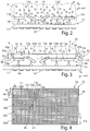
- the protective element 30 additionally has a frame 34 in the form of a (wire) grid, of which only two webs 35 are illustrated in Figure 3 .
- a first membrane segment 33a, which is on the left in Figure 3 , and a second membrane segment 33b, which is in the middle in Figure 3 are fastened at the edge to a first web 35a.
- the middle membrane segment 33b and a membrane segment 33c that is on the right in Figure 3 are fastened at the edge to a second web 35b.
- the fastening of the membrane segments 33a-c to the webs 35a,b may take place by adhesive bonding or in some other way.
- adjacent membrane segments 33a,b; 33b,c directly adjoin one another, and so the entire upper side of the webs 35a, 35b is covered by the membrane segments 33a-c.
- the middle membrane segment 33b covers a partial region T of the surface 31 that comprises the five facet elements 33a-e illustrated in Figure 3 and protects it from the contaminating substances P.
- the first and third membrane segments 33a, 33c which likewise cover a respective partial region of the surface 31, as can be seen in particular from Figure 4 , which shows the optical assembly 32 in a plan view from above, i.e. looking onto the protective element 30.
- the grid-shaped frame 34 of the protective element 30 can be seen, in the example shown comprising five webs arranged in parallel in the longitudinal direction and four webs arranged in parallel in the transverse direction, which are respectively connected to one another at grid nodes. Between every two webs 35 that are adjacent in the longitudinal direction or in the transverse direction there is respectively arranged one of altogether twelve membrane segments, which cover in a planar manner the surface 31 to be protected of the field facet element 13.
- a first membrane segment 33a to a fourth membrane segment 33d in the transverse direction of the field facet mirror 13 are denoted by way of example.
- the field facet mirror 13 arranged under the protective element 30 has a grid-shaped arrangement of 15 x 20 facet elements, of which only five facet elements 13a-e, arranged in a common column, are denoted by reference signs in Figure 4 . It goes without saying that the number of 15 x 20 facet elements has only been chosen for purposes of illustration and that the actual number of facet elements may possibly be much greater.
- the facet elements are respectively arranged in groups of 5 x 5 facet elements, between which there is formed an intermediate space 36 (cf. also Figure 3 ), which is typically larger than an intermediate space 37 between adjacent facet elements 13a-e of the same group.
- a respective membrane element 35a-c covers a group of 5 x 5 facet elements, the webs 35 of the frame 34 being arranged over the intermediate spaces 36 (see also Figure 3 ) between adjacent groups of facet elements.
- the protective element 30 is arranged at a comparatively small distance A from the surface 31 of the facet mirror 13, which may for example be less than 10 mm, preferably less than 5 mm, particularly preferably less than 2 mm, and which is at least great enough that a tilted facet element 13b, 13c does not bump into the protective element 30 or a respective membrane segment 33a-c.
- the distance between the protective element 30 and the surface 31 to be protected is measured here between the respective membrane segments 33a-c, to be more precise between the side thereof that is facing the field facet mirror 13, and the surface 31.
- the protective element 30 of the optical assembly 32 may be fastened to a mounting, to which the field facet element 13 itself is also fastened, but it is also possible that the field facet element 13 and the frame 34 are fastened to different mountings that are kept at a distance from one another.
- the protective element 30 may be fastened to the mounting in a detachable way, i.e. via a detachable connection such as a screw connection or a clamping connection. This facilitates the removal of the protective element 30 from the EUV lithography apparatus, should this possibly be required because of contamination of the membrane segments 33a-c.
- the geometry, i.e. the length and the width, of the grid-shaped frame 34 is adapted to the geometry, i.e. the length and width, of the facet elements 13a-e, to be precise in such a way that the webs 35 of the frame 34 are arranged over the intermediate spaces 36 between the adjacent groups of facet elements.
- a respective facet element 13a-e has a linear extent in the X direction (length) L of about 3 mm and a linear extent in the Y direction (width) B of about 1 mm.
- the linear extent 5 x L, 5 x B of a respective membrane segment 33a-c corresponds approximately to an integral multiple of the length L and the width B of a respective facet element 13a-e.
- the length and the width of a respective membrane segment 33a-c are typically slightly greater than an integral multiple of the length L and the width B of a respective facet element 13a-e, i.e. 5 x (L + L Z ) and 6 x (B + B Z ), where L Z , B Z denote the length and the width of a respective intermediate space 37 between adjacent facet elements 13a-e.
- a respective membrane element 33a-c may cover a smaller number of facet elements, in particular only a single facet element 13a-e.
- the aspect ratio, i.e. the ratio of length to width, of a respective partial region of the frame 34 that is delimited by four webs 35 substantially coincides with the aspect ratio, i.e. the ratio of length to width, of the respectively covered facet element 13a-e.
- the membrane segments 33a-c which together cover the surface 31 of the field facet mirror 13, are formed from polycrystalline silicon, which has a low absorption with respect to the EUV radiation 4.
- the membrane segments 33a-c should not have too great a thickness D, typical values for the thickness D lying between about 5 nm and about 500 nm.
- a coating 38 has been applied to the membrane segments 33a-c on the side thereof that is facing away from the field facet mirror 13. Fewer contaminating particles P are deposited on the coating 38 than would be the case with the uncoated material of the membrane segments 33a-c. Oxides, nitrides, carbides and borides have been found to be advantageous as the material for the coating 38.
- oxides have proven in particular to be advantageous as coating materials, for example titanium oxide, zirconium oxide, yttrium oxide, cerium oxide, niobium oxide, lanthanum oxide, vanadium oxide, chromium oxide, manganese oxide, aluminum oxide, cobalt oxide, molybdenum oxide and tungsten oxide.
- titanium oxide, zirconium oxide, yttrium oxide, cerium oxide, niobium oxide, lanthanum oxide, vanadium oxide, chromium oxide, manganese oxide, aluminum oxide, cobalt oxide, molybdenum oxide and tungsten oxide In particular in the case of a coating 38 of ZrO 2 , it has been found that a surface region affected by tin contamination was reduced in the size of its surface area under the effect of EUV radiation 4. The probability of (molecular) tin contaminants being deposited on the surface of a coating 38 of ZrO 2 during the exposure operation of the EUV lithography system 1 is therefore very low.
- the optical assembly 32 with the field facet mirror 13 that is shown in Figure 3 and Figure 4 may be arranged in the illumination system 10 of the EUV lithography apparatus 1 from Figure 1 .
- the EUV lithography apparatus 1 has a cleaning device 39 for removing contaminating substances P from a side facing away from the optical element 13 of the membrane 33a-c of the optical assembly 32 that is shown in Figure 3 .
- the cleaning device 39 is designed to direct a cleaning gas 40, for example (possibly activated) hydrogen, onto the optical element 13.
- the cleaning device 39 has a nozzle, from which the cleaning gas 40 flows out and impinges on the side facing away from the optical element 13 of the membrane 33a-c that is shown in Figure 3 .
- the cleaning gas 40 is extracted from a gas reservoir (not shown in Figure 1 ).
- the cleaning device 39 or at least the partial region from which the cleaning gas 40 leaves, can be moved within the EUV lithography apparatus 1, in order to clean different partial regions of the membrane 33a-c or prevent the cleaning device 39 from protruding into the illumination beam 4 of the illumination system 10 during exposure operation.
- the optical assembly 32 comprises a purge device 41 for purging a space 44 between the optical element 13 and the side of the membrane 33a-c that is facing the optical element 13 with a purge gas 42.
- the purge gas 42 is extracted from a gas reservoir and provided to a nozzle 43 of the purge device 41 from which the purge gas 42 flows out into the space 44.
- the space 44 between the membrane 33a-c and the optical element 13 is separated from the remainder of the vacuum environment of the EUV lithography system 1 in a gas-tight manner.
- the purge device 41 has a suction unit (not shown) for removing the purge gas 42 from the space 44.
- a plurality of gases may be used as a purge gas 42, for instance, hydrogen, noble gases such as helium or gases having a larger molecular weight such as nitrogen.
- a further optical assembly which contains the pupil facet mirror 14 as an optical element, may be arranged in the illumination system 10 from Figure 1 .
- the mirrors 21 to 24 in the projection system 20 or in other optical arrangements, for example in EUV lithographic metrology systems, may possibly be provided with corresponding protective elements 30 in order to protect them from contaminating substances P.
- a transmissive optical element instead of a reflective optical element, may also be protected from contaminating substances with a protective element. In particular, the area of use of such a protective element is not restricted to EUV lithography applications.
Landscapes
- Physics & Mathematics (AREA)
- General Physics & Mathematics (AREA)
- Optics & Photonics (AREA)
- Public Health (AREA)
- Life Sciences & Earth Sciences (AREA)
- Atmospheric Sciences (AREA)
- Health & Medical Sciences (AREA)
- Epidemiology (AREA)
- Engineering & Computer Science (AREA)
- Environmental & Geological Engineering (AREA)
- Chemical Kinetics & Catalysis (AREA)
- Chemical & Material Sciences (AREA)
- Exposure And Positioning Against Photoresist Photosensitive Materials (AREA)
- Optical Elements Other Than Lenses (AREA)
Description
- The invention relates to an optical assembly comprising: an optical element, in particular for the reflection of EUV radiation, and a protective element for protecting a surface of the optical element from contaminating substances, the protective element comprising a membrane and a frame on which the membrane is mounted. The membrane is formed by a plurality of membrane segments, which respectively protect a partial region of the surface of the optical element from the contaminating substances. The optical element is a facet mirror with a plurality of facet elements. The invention also relates to an optical arrangement, for example an EUV lithography system, with at least one such optical assembly.
- Such an optical assembly is known from
DE 10 2012 204295 A1 . -
US 2011/309271 A1 discloses a spectral purity filter that includes a plurality of segments that each includes a mesh in which an array of apertures of an aperture size at or below a predetermined size is formed and which has electroconductivity; and a frame that supports the plurality of the segments at least at a periphery thereof. -
US 2006/245044 A1 discloses a method of manufacturing a filter for retaining a substance originating from a radiation source, which filter comprises a thin layer that is transparent to extreme ultraviolet radiation. The thin layer may be connected to the support structure in a high-temperature-resistant manner. - For the purposes of this application, an EUV lithography system is understood as meaning an optical system or an optical arrangement for EUV lithography, i.e. an optical system that can be used in the field of EUV lithography. Apart from an EUV lithography apparatus, which serves for the production of semiconductor components, the optical system may be for example an inspection system for the inspection of a photomask used in an EUV lithography apparatus (hereinafter also referred to as a reticle), for the inspection of a semiconductor substrate to be structured (hereinafter also referred to as a wafer) or a metrology system, which is used for measuring an EUV lithography apparatus or parts thereof, for example for measuring a projection system.
- When using EUV radiation at wavelengths in the range between about 5 nm and about 30 nm, for example in EUV lithography apparatuses, the contamination of optical elements by contaminating substances presents a particular problem. Contaminating substances may be produced for example in an EUV light source in which a target material, for example in the form of tin droplets, is used for generating the EUV radiation. The target material in the form of tin droplets may be transformed into a plasma state by a laser beam, whereby the tin droplets partially evaporate and tin particles are produced. The tin particles can spread out in the EUV lithography apparatus and be deposited either directly or in the form of a layer of tin on the optical surface of optical elements, for example in the illumination system or in the projection system, and also on mechanical or mechatronic components of the EUV lithography apparatus.
- The contamination of the surfaces by tin particles can take place in various ways: The tin particles may be deposited on the optical surfaces directly from the gas phase or a layer of tin may be produced by surface diffusion of tin. Contaminations by tin can also be caused by outgassing effects on tin-containing components in the EUV lithography apparatus that are induced by hydrogen or a hydrogen plasma present in the EUV lithography apparatus. The depositing of tin on the optical surfaces of the optical elements may also bring about blistering in a reflective coating of the optical elements, which in the worst case has the consequence of delamination of the coating. Mechatronic components may also be greatly restricted in their functioning or destroyed by penetrating Sn particles.
- It is known to protect masks or wafers that are used in lithography systems from contaminating substances with the aid of protective elements in the form of so-called pellicles. A pellicle is a membrane which consists of a material that is transparent, or as unabsorbent as possible, with respect to the radiation at the wavelength of the lithography system. In particular when using EUV radiation, the thickness of such a pellicle is typically small, in order to keep the absorption of the radiation passing through the pellicle as low as possible.
-
US 7,829,248 B2 discloses a mask-pellicle system for lithography in which a pellicle is arranged in the vicinity of a transparent substrate of the mask. The pellicle is fastened to a frame, which rests on the mask. Mounted on the frame is a device that absorbs mechanical stresses. The frame has at least two segments, which are connected to one another at an angle in order to protect the stress-absorbing device from radiation energy from the lithography process. -
EP 1 791 027 A1 describes a lithography apparatus for immersion lithography, which has a supporting table for holding an object, for example a substrate. In order to minimize the formation of bubbles in the immersion medium, a gap between the object and the supporting table is to be minimized. For this purpose, a covering plate may be provided and in one example is formed as a pellicle that is mounted on the outside of the supporting table. In another example, the covering plate is segmented, the segments of the covering plate sliding over one another. -
US 2010/0195076 A1 has disclosed an optical membrane element for a lithography device, said membrane element comprising at least one membrane layer and a frame, which at least partially surrounds the at least one membrane layer and to which at least part of the edge of the membrane layer is fastened. - At least one tensioning element is provided for clamping the membrane in an adjustable manner. In an EUV lithography apparatus, the membrane element may be arranged for example in front of a mirror of an illumination system and serve as a neutral grey filter.
- The object of the invention is to provide an optical assembly and an optical arrangement, in particular an EUV lithography system, with at least one such optical assembly, in which an optical element that has a comparatively large surface to be protected can be effectively protected from contaminating substances
- This object is achieved by an optical assembly of the type mentioned at the beginning, wherein the geometry of the frame is adapted to the geometry of the facet elements.
- When the optical element is arranged in an optical arrangement for EUV lithography, the membrane may additionally protect the optical element from a plasma caused by EUV radiation in the vacuum environment thereof. When using a one-part membrane for protecting a surface from contaminating substances, there is the problem that such a membrane cannot be readily produced with any desired surface area. There is also the problem that, because of its small thickness, the membrane is not self-supporting, and so has a tendency to bend, the bending typically being all the greater the larger the surface of the membrane is. In
US 2010/0195076 A1 , cited at the beginning, it is proposed to counteract the bending of the membrane by the membrane being laterally clamped. InUS 2010/0195076 A1 it is stated that such a membrane typically does not exceed a maximum edge length of 200 mm. Large optical elements however have a surface or an edge length that is possibly greater than 200 mm, and so the surface of such an optical element typically cannot be completely protected from contaminating substances with a one-part membrane. - Using a multi-part membrane, i.e. a membrane that has a plurality of membrane segments, allows the area or the surface region that is protected from contaminating substances by the protective element to be increased significantly in size. The membrane segments are typically mounted on a common frame, which has a much greater thickness than the membrane and is self-supporting. The plurality of membrane segments that are mounted in the frame typically cover the optical surface completely, or at least that partial region of the optical surface on which radiation, for example EUV radiation, is incident.
- In particular when using EUV radiation, there is the problem that no materials that are substantially transparent to the wavelengths of less than 13.5 nm used in that case exist. The frame, which typically has a much greater thickness than the membrane, is therefore generally not transparent to the EUV radiation, irrespective of the choice of material. The frame, to be more precise the parts of the frame that are arranged in the beam path, consequently shade the surface of the optical element in a partial region corresponding to the projection of the frame onto the surface.
- In one embodiment, the frame has a plurality of webs for the fastening of the respective membrane segments at the edges. The frame, to be more precise the webs of the frame, surround the respective membrane segments at least partially, in particular completely. Generally, a respective membrane segment rests with its edge completely on the webs or is fastened at its edge to the webs. The membrane segments may be fastened to the webs of the frame by an adhesive connection or in some other way. The webs may be formed in the manner of a raster or a grid, the membrane segments being arranged in the meshes between the webs of the grid. The frame or the webs of the frame may be formed from a material suitable for vacuum environments, such as for example high-grade steel, a metal such as aluminum, etc. The frame may be formed in particular as a wire grid.
- In order to keep the shading of the optical element by the frame as low as possible, the webs of the frame should have a width that is as small as possible, on the other hand the width should be sufficient for the fastening of the membrane segments. Typically, an edge of a membrane segment is respectively fastened on two longitudinal sides of a web lying opposite one another. Ideally, the edges of two adjacent membrane segments lie flush against one another at a respective web, and so the segmented membrane covers the entire surface to be protected of the optical element in a planar manner. It is also possible that the edges of adjacent membrane segments are fastened to a web at a distance from one another, so that the web is not completely covered by the membrane, but the surface is nevertheless covered in a planar manner. In this case, at least the partial region of the web between the membrane segments is exposed to contaminating substances. For protection from the contaminating substances, the web may possibly be provided at least in the non-covered partial region with a coating. Two membrane segments that are mounted on a web may possibly overlap one another.
- In one embodiment, the optical element has at least one actuator for moving at least one partial region of the surface. The optical element may be for example a mirror, the (optical) surface of which is tilted, or possibly linearly displaced, with the aid of the actuator. Such a mirror may however also have a number of partial regions that can be moved individually, for example tilted or displaced. With such actuable mirrors, there is in principle the problem that partial regions of the actuator that are arranged in the region of the surface possibly come into contact with the contaminating substances and are impaired in their functioning.
- The optical element is a segmented mirror with a plurality of mirror segments, more precisely a facet mirror with a plurality of facet elements. A segmented mirror comprises a plurality of mirror segments, each forming a partial region of the mirror surface, the mirror segments being typically arranged adjacent to each other. The mirror segments may be actuable individually, for example tilted or displaced, or the mirror segments may not be actuable at all. The latter may be the case when the surface area of the mirror is too large so that it cannot be manufactured as one piece.
- Facet mirrors constitute a special case of segmented mirrors which are used for example in illumination systems of EUV lithography apparatuses in order to produce a homogenization of the radiation generated by an EUV light source on an illumination area that is illuminated by the illumination system. Such facet mirrors often have at least in one spatial direction a comparatively great edge length, which may for example be several 100 mm to 1000 mm, or possibly more, and so the surface of such a facet mirror generally cannot be protected by a one-piece membrane. For example, such a facet mirror may have a linear extent (length x width) of more than 800 mm x 800 mm, which is typically too large to be covered by a one-piece membrane. Although the following description relates to facet mirrors and facet elements one skilled in the art will readily understand that the principles described below are are also applicable to the more general case of segmented mirrors.
- The facet elements of such a facet mirror can in general be actuated with the aid of actuators, i.e. can be individually moved, in particular tilted. The facet mirror typically has mechanical or mechatronic components as actuators. For this purpose, the facet mirror may for example be formed as an MEMS ("micro-electro-mechanical system") mirror. The electromechanical components on the surface of such a facet mirror are not covered - in particular when individual facet elements are tilted - and are exposed to the contaminating substances, which may have the effect that their function is impaired, which can be prevented by the protective element.
- The geometry of the frame is adapted to the geometry of the facet elements. The geometry of the facet elements is typically adapted to the illumination field to be illuminated. The facet elements may for example have a rectangular, square, hexagonal... geometry. If the facet elements have for example a rectangular or square geometry, the geometry of the frame is in this case also correspondingly adapted, i.e. the webs of the frame are likewise arranged in rows and columns.
- In a further embodiment, the webs of the frame are arranged over intermediate spaces between the facet elements. Between adjacent facet elements of the facet mirror there is typically formed an intermediate space, in which the incident radiation is not reflected by the facet elements. Since, when using EUV radiation, the webs of the frame are not transparent to the incident radiation, it is advantageous if the webs, to be more precise the "shadow" of the webs in the projection onto the surface to be protected, falls in the intermediate spaces between the facet elements, since no radiation is reflected from the facet mirror there in any case. It proves to be advantageous here if the protective element is arranged at a small distance in front of the surface to be protected, since in this case the position of the shadow cast by the webs of the frame is substantially independent of the direction in which the radiation to be reflected is incident on the facet mirror. It goes without saying that, in this exemplary embodiment, the webs should have a width that is less than the width of the intermediate spaces between the facet elements over which the webs are arranged.
- In a further embodiment, the (segmented) membrane is arranged at a distance of less than 10 mm, preferably of less than 5 mm, particularly preferably of less than 2 mm, from the surface of the optical element. In the case of an optical element in the form of a facet mirror, the surface from which the distance is measured is the plane in which the facet elements in the untilted state are arranged. As described further above, a small distance has an advantageous effect on the shading of the facet mirror by the webs of the frame. However, the distance should be chosen to be sufficiently great to avoid the facet elements colliding with the membrane or with the webs of the frame during tilting.
- In a further embodiment, the linear extent of a membrane segment corresponds substantially to an integral multiple (typically other than one) of the linear extent of a facet element. It is typically not absolutely necessary that a respective membrane segment covers only a single facet element; rather, a single membrane segment may cover a number of facet elements, for example a group of N x M facet elements. In this case, the linear extent of the membrane segment in two directions perpendicular to one another corresponds (approximately) to N times or M times the linear extent of a respective facet element. Since intermediate spaces are formed between the facet elements, the linear extent of a membrane segment is typically somewhat greater than an integral multiple of a single facet element, the deviation typically being no greater than about 20%, preferably no greater than 10%. A substantially integral multiple of the linear extent of the facet element is understood as meaning such a deviation of the linear extent of the membrane segment.
- Ideally, the linear extent in the longitudinal direction of at least one membrane segment corresponds to an integral multiple of the sum of the length of a facet element and the distance in the longitudinal direction between adjacent facet elements. Correspondingly, the linear extent in the widthwise direction of the at least one membrane segment corresponds to an integral multiple of the sum of the width of the facet element and the distance in the widthwise direction between adjacent facet elements. It goes without saying that adjacent webs of the frame are typically arranged at a corresponding distance (i.e. approximately N times or M times the linear extent of a facet element) from one another.
- In the case of facet mirrors, the facet elements are often arranged in groups of N x M facet elements, the distance between adjacent groups being greater than the distance between adjacent facet elements. In order to keep the shading as low as possible, it may be advantageous to choose the linear extent of the membrane segments in such a way that the linear extent of a membrane segment corresponds to an integral multiple or exactly the linear extent of such a group of N x M facet elements.
- In one embodiment, the membrane is formed from silicon, in particular from polysilicon. It has been found that this material has a low absorption, and consequently a high transmission, with respect to EUV radiation. A thin membrane of (poly)silicon may for example have a mean transmission of more than 85% of the incident EUV radiation.
- In a further embodiment, the membrane segments have on a side facing away from the optical element a coating that reduces the attachment of contaminating substances. The material of the membrane that is optimized with regard to the transmission of EUV radiation is typically not optimized with regard to lowest possible attachment of contaminating substances, and so it has proven to be advantageous to apply to the membrane a coating with which the attachment of contaminating substances is less than in the case of the material of the membrane.
- In one embodiment, the material of the coating is selected from the group comprising: oxides, nitrides, carbides and borides. The choice of a suitable material for the coating depends on the type or chemical composition of the contaminating substances from which the optical element is to be protected, for example tin contaminants. In the case of certain types of contaminating substances, the coating should typically not comprise any (pure) metals. It goes without saying that, when using the optical assembly for EUV lithography, the coating of the membrane must withstand the vacuum conditions in an EUV lithography system.
- In a further embodiment, the material of the coating is selected from the group: titanium oxide, zirconium oxide, yttrium oxide, cerium oxide, niobium oxide, lanthanum oxide, vanadium oxide, chromium oxide, manganese oxide, aluminum oxide, cobalt oxide, molybdenum oxide and tungsten oxide. These materials have proven to be advantageous in particular for reducing the attachment of tin contaminants (in the form of tin or for example tin hydrides). For example, it has been found in experiments that the surface region or the volume of tin particles that attach themselves to a surface coated with ZrO2 was reduced when it was exposed to a hydrogen plasma such as that which is induced in the vacuum environment of an EUV lithography system, for example by EUV radiation.
- In addition or as an alternative to a coating for providing protection from contaminating substances, the membrane may have a functional coating that serves another purpose. For example, the coating may serve as a spectral filter, in order to filter out the desired EUV wavelength range from the radiation emitted by the EUV light source. A coating which performs the function of a neutral grey filter is also possible.
- In a further embodiment, the membrane segments each have a thickness of between 5 nm and 500 nm. As described further above, the membrane segments should not have too great a thickness, in order to make it possible for the membrane to have the highest possible transmission of the EUV radiation. However, the thickness of the membrane should also not be chosen to be too small, in order to prevent the membrane from tearing through, for example when too great an amount of contaminating substances becomes attached.
- In another embodiment, the protective element is mounted in the optical assembly in a detachable way, i.e. via a detachable connection, e.g. a screw connection, a clamping connection, etc. The optical assembly may comprise a mounting which holds the protective element at a predetermined distance from the surface of the optical element, the protective element being connected to the mounting in a detachable manner. In this way, the protective element may be replaced in a cost-saving and time-saving manner without having to replace the optical element. Replacement of the protective element may be required e.g. when an excessive amount of contaminating substances has accumulated on the side of the membrane segments facing away from the optical element.
- In a further embodiment, the optical assembly comprises a purge device for purging a space between the optical element and the side of the membrane that is facing the optical element with a purge gas. The space between the membrane and the optical element forms a so-called mini-environment which is separated from the remainder of the (vacuum) environment of the optical arrangement in which the optical assembly is arranged. The space between the membrane and the optical element may be separated from the environment in a gas-tight manner, but this is not necessarily the case. In either case, by providing a dedicated purge gas flow through the space, contaminating substances which are outgassed from the optical element may be prevented from reaching the vacuum environment outside of the mini-environment. The purge device typically has a nozzle from which the purge gas flows out into the space between the membrane and the optical element. The purge device may also comprise a suction unit for removing the purge gas from the space between the optical element and the membrane. A plurality of gases may be used as a purge gas. For instance, hydrogen or noble gases such as helium may be used, but also heavier gases having a larger molecular weight such as nitrogen may be used. These heavier gases can be applied as purge gases despite their typically higher light absorption per length of optical path at similar pressures (higher than, e.g. hydrogen), without too much loss of light intensity of the EUV light beam, because the length the light beam has to pass (twice) in the space between the optical surface and the nearby membrane is limited (typically in the range of only a few mm).
- A further aspect of the invention relates to an optical arrangement, in particular an EUV lithography system, comprising at least one optical assembly as described further above. The optical assembly or the optical assemblies may serve in particular for the protection of optical elements that have a comparatively large optically used surface. This is typically the case with facet mirrors in the illumination system of an EUV lithography apparatus, but also other, possibly faceted optical elements can be effectively protected from contaminating substances by the protective element described further above.
- In one embodiment, the optical arrangement has at least one cleaning device for removing contaminating substances from a side of the membrane that is facing away from the optical element. The cleaning device is designed to bring the side of the membrane that is facing away from the optical element into contact with a cleaning agent, in particular with a cleaning gas, for example with (possibly activated) hydrogen. The cleaning device typically has in this case a nozzle, from which the cleaning gas flows out and impinges on the side of the membrane that is facing away from the optical element. For this purpose, the cleaning gas is typically removed from a gas reservoir and fed to the nozzle. The part of the cleaning device with the nozzle may possibly be moved in the optical arrangement, in order to clean different partial regions of the membrane, or in order to make it possible that the nozzle or the entire cleaning device is arranged outside the beam path during the operation of the optical arrangement. The contaminating substances may be particles or molecular contaminants.
- In one embodiment, the optical arrangement has an illumination system and the optical assembly is arranged in the illumination system, the optical element of the optical assembly being formed by a facet mirror of the illumination system.
- As described further above, by the nature of their construction, facet mirrors have a relatively large surface. Since the facet elements of such facet mirrors are typically actuated by mechanical or electromechanical components, which can possibly be damaged by the contaminating substances, it is advantageous to protect such a facet mirror from contaminating substances.
- Further features and advantages of the invention emerge from the following description of exemplary embodiments of the invention, on the basis of the figures in the drawing, which show details essential to the invention, and from the claims. The individual features can be realized respectively on their own or together in any combination in one variant of the invention.
- Exemplary embodiments are illustrated in the schematic drawing and are explained in the following description. In the figures
- Figure 1
- shows a schematic illustration of an EUV lithography apparatus with two facet mirrors,
- Figure 2
- shows a schematic illustration of a detail of a facet mirror from
Figure 1 , the surface of which is exposed to contaminating substances, in a side view, - Figure 3
- shows a schematic illustration of a detail of a facet mirror from
Figure 1 , the surface of which is protected from contaminating substances by a protective element with a number of membrane segments, in a side view, and - Figure 4
- shows a schematic illustration of the facet mirror from
Figure 1 with the protective element arranged in front of the surface thereof, in a plan view. - Identical reference signs are used in the following description of the drawings for components that are the same or functionally the same.
- In
Figure 1 , an optical arrangement in the form of an EUV lithography system, to be more precise an EUV lithography apparatus 1, is schematically shown. It has an EUVlight source 2 for generating EUV radiation, which has a high energy density in an EUV wavelength range below 50 nm, in particular between about 5 nm and about 15 nm. The EUVlight source 2 may for example take the form of a plasma light source for generating a laser-induced plasma or be formed as a synchrotron radiation source. In particular in the former case, acollector mirror 3 may be used, as shown inFigure 1 , in order to focus the EUV radiation of the EUVlight source 2 into anillumination beam 4 and in this way increase the energy density further. Theillumination beam 4 has a wavelength spectrum, which is concentrated in a narrowband wavelength range around an operating wavelength λB, at which the EUV lithography apparatus 1 is operated. Amonochromator 12 is used for selecting the operating wavelength λB or for selecting the narrowband wavelength range. - The
illumination beam 4 serves for the illumination of a structured object M by means of anillumination system 10, which in the present example has four reflectiveoptical elements 13 to 16. The structured object M may be for example a reflective mask M, which has reflective and non-reflective, or at least much less reflective, regions for producing at least one structure on the object M. Alternatively, the structured object M may be a plurality of micro-mirrors, which are arranged in a one-dimensional or multi-dimensional arrangement and which are possibly movable about at least one axis, in order to set the angle of incidence of theEUV radiation 4 on the respective mirror. - The structured object M reflects part of the
illumination beam 4 and forms aprojection beam 5, which carries the information about the structure of the structured object M and is radiated into aprojection system 20, which produces a projected image of the structured object M or of a respective partial region thereof on a substrate W, for which purpose four reflectiveoptical elements 21 to 24 are arranged in theprojection system 20. The substrate W, for example a wafer, comprises a semiconductor material, for example silicon, and is arranged on a mounting, which is also referred to as a wafer stage WS. - The first and second reflective elements in the
illumination system 10 are in the present case formed as segmented mirrors in the form of facet mirrors 13, 14 and have a plurality offacet elements 13a-d, 14a-d in the form of micro-mirrors, which are respectively arranged in a raster arrangement. For eachfacet mirror facet elements 13a-d, 14a-d, at which theillumination beam 4 or a respective partial beam of theillumination beam 4 is reflected, are shown by way of example inFigure 1 . The firstoptical element 13 is subsequently also referred to as thefield facet mirror 13 and serves for producing secondary light sources in theillumination system 10. The secondoptical element 14 is typically arranged at the location of the secondary light sources produced by the firstoptical element 13 and is subsequently also referred to as thepupil facet mirror 14. - A partial beam of the
illumination beam 4 that is incident on arespective facet element 13a-d of thefield facet mirror 13 is deflected at it onto arespective facet element 14a-d of thepupil facet mirror 14. Thefacet elements 13a-d of thefield facet mirror 13 may be rectangular and have an aspect ratio (x : y) of for example 20 : 1 or less, the X direction extending perpendicularly to the plane of the drawing ofFigure 1 . The aspect ratio of thefacet elements 13a-d corresponds here to the aspect ratio of the illumination field that is illuminated by theillumination system 10, and is for example rectangular. It goes without saying that illumination fields orfacet elements 13a-d with a geometry other than rectangular are likewise possible. - Each of the
facet elements 13a-d of thefield facet mirror 13 may in the present case be tilted about an axial direction parallel to the X direction, as indicated by way of example inFigure 1 by two angular positions W1, W2 of thefirst facet element 13a of thefield facet mirror 13. In addition, arespective facet element 13a-d may possibly also be tiltable about a further axis that lies in the XZ plane (plane of the drawing). In this way, the direction in which theillumination beam 4 is incident on thefacet elements 13a-d can be set. The tilting can also have the effect in particular of changing the assignment between thefacet elements 13a-d of thefield facet mirror 13 and thefacet elements 14a-d of thepupil facet mirror 14, in order to produce a desired illumination distribution (illumination pupil or angular distribution) at the location of the illuminated object M. Correspondingly, thefacet elements 14a-d of thepupil facet mirror 14 may also be tiltable about an axial direction parallel to the X direction and possibly about a further axis that lies in the XZ plane (plane of the drawing). - In the example shown, the EUV
light source 2 is formed as a plasma light source for generating a laser-induced plasma on a target material, which takes the form of tin droplets. During the formation of the plasma, some of the tin material of the EUVlight source 2 goes over into the gas phase and forms contaminating substances P in the form of tin contaminants, for example tin particles or tin compounds, in particular tin hydrides (SnxHY). The contaminating substances P may spread out in the EUV lithography apparatus 1 from the EUVlight source 2 to optical elements, for example to thefield facet mirror 13 or to thepupil facet mirror 14, and be deposited on them or contaminate them. -
Figure 2 shows a detail of thefield facet mirror 13 fromFigure 1 , with by way of example fivefacet elements 13a-e, which are exposed to the contaminating substances P. As can be seen inFigure 2 , thefield facet mirror 13 has asubstrate 17 of silicon, which has columnar supportingelements 18, on which thefacet elements 13a-e are movably mounted. Mounted underneath thesubstrate 17 in the region of eachfacet element 13a-e is/are one ormore actuators 19, for example in the form of electrodes, for producing an electrical field, in order to tilt thefacet elements 13a-e by means of electrostatic attraction about an axis that extends in the X direction and runs in the region of a respective supportingelement 18. - As can be seen in
Figure 2 , the contaminating substances P may not only be deposited on the surfaces of thefacet elements 13a-e themselves, on which a coating that reflects theEUV radiation 4 has been applied, but may also enter an intermediate space betweenadjacent facet elements 13a-e and settle on a respective supportingelement 18 and/or on thesubstrate 17 of thefacet mirror 13. This applies in particular ifindividual facet elements 13a-e are tilted out of a common plane, indicated inFigure 2 by dashed lines, as is the case with the second andthird facet elements Figure 2 . - The deposition of contaminating substances P in the form of tin particles may change the electrical potential on the surface of the supporting
elements 18, whereby the actuation or tilting of thefacet elements 13a-e by theactuators 19 is impaired. In particular, the angular range in which the actuation of thefacet elements 13a-e is possible may be restricted by the deposition of the contaminating substances P. -
Figure 3 shows thefacet mirror 13 fromFigure 2 , arranged in front of which is aprotective element 30, which protects thefacet mirror 13, to be more precise theplanar surface 31 thereof, which is illustrated inFigure 3 by dashed lines and along which thefacet elements 13a-e in the non-tilted state are arranged with their upper sides facing theEUV radiation 4, from the contaminating substances P. Together with theprotective element 30, thefacet mirror 13 forms anoptical assembly 32. - In the example shown, the
protective element 30 has a membrane, which is formed by a plurality ofmembrane segments 33a-c, of which threemembrane segments 33a-c are at least partially illustrated inFigure 3 by way of example. Theprotective element 30 additionally has aframe 34 in the form of a (wire) grid, of which only twowebs 35 are illustrated inFigure 3 . Afirst membrane segment 33a, which is on the left inFigure 3 , and asecond membrane segment 33b, which is in the middle inFigure 3 , are fastened at the edge to afirst web 35a. Correspondingly, themiddle membrane segment 33b and amembrane segment 33c that is on the right inFigure 3 are fastened at the edge to a second web 35b. The fastening of themembrane segments 33a-c to thewebs 35a,b may take place by adhesive bonding or in some other way. - In the example shown,
adjacent membrane segments 33a,b; 33b,c directly adjoin one another, and so the entire upper side of thewebs 35a, 35b is covered by themembrane segments 33a-c. As can likewise be seen inFigure 3 , themiddle membrane segment 33b covers a partial region T of thesurface 31 that comprises the fivefacet elements 33a-e illustrated inFigure 3 and protects it from the contaminating substances P. The same applies to the first andthird membrane segments surface 31, as can be seen in particular fromFigure 4 , which shows theoptical assembly 32 in a plan view from above, i.e. looking onto theprotective element 30. - In
Figure 4 , the grid-shapedframe 34 of theprotective element 30 can be seen, in the example shown comprising five webs arranged in parallel in the longitudinal direction and four webs arranged in parallel in the transverse direction, which are respectively connected to one another at grid nodes. Between every twowebs 35 that are adjacent in the longitudinal direction or in the transverse direction there is respectively arranged one of altogether twelve membrane segments, which cover in a planar manner thesurface 31 to be protected of thefield facet element 13. - In
Figure 4 , only afirst membrane segment 33a to afourth membrane segment 33d in the transverse direction of thefield facet mirror 13 are denoted by way of example. In the example shown, thefield facet mirror 13 arranged under theprotective element 30 has a grid-shaped arrangement of 15 x 20 facet elements, of which only fivefacet elements 13a-e, arranged in a common column, are denoted by reference signs inFigure 4 . It goes without saying that the number of 15 x 20 facet elements has only been chosen for purposes of illustration and that the actual number of facet elements may possibly be much greater. - In the case of the
field facet mirror 13 shown inFigure 4 , the facet elements are respectively arranged in groups of 5 x 5 facet elements, between which there is formed an intermediate space 36 (cf. alsoFigure 3 ), which is typically larger than anintermediate space 37 betweenadjacent facet elements 13a-e of the same group. Arespective membrane element 35a-c covers a group of 5 x 5 facet elements, thewebs 35 of theframe 34 being arranged over the intermediate spaces 36 (see alsoFigure 3 ) between adjacent groups of facet elements. In this way, only a partial region of thesurface 31, which in any case cannot contribute to the reflection ofEUV radiation 4 since nofacet elements 13a-e are arranged there, is shaded by theframe 34, to be more precise by thewebs 35. - In order also in the case of
EUV radiation 4 that is possibly obliquely incident on thesurface 31 of thefield facet mirror 13 to prevent thewebs 35 of theframe 34, which are formed from a material that is not transparent to theEUV radiation 4, for example from aluminum, from being able to shade the reflective surfaces of thefacet elements 13a-e, it is advantageous if theprotective element 30 is arranged at a comparatively small distance A from thesurface 31 of thefacet mirror 13, which may for example be less than 10 mm, preferably less than 5 mm, particularly preferably less than 2 mm, and which is at least great enough that a tiltedfacet element protective element 30 or arespective membrane segment 33a-c. The distance between theprotective element 30 and thesurface 31 to be protected is measured here between therespective membrane segments 33a-c, to be more precise between the side thereof that is facing thefield facet mirror 13, and thesurface 31. - The
protective element 30 of theoptical assembly 32, to be more precise theframe 34 of theprotective element 30, may be fastened to a mounting, to which thefield facet element 13 itself is also fastened, but it is also possible that thefield facet element 13 and theframe 34 are fastened to different mountings that are kept at a distance from one another. In either case, theprotective element 30 may be fastened to the mounting in a detachable way, i.e. via a detachable connection such as a screw connection or a clamping connection. This facilitates the removal of theprotective element 30 from the EUV lithography apparatus, should this possibly be required because of contamination of themembrane segments 33a-c. - In the case of the example shown in
Figure 4 , the geometry, i.e. the length and the width, of the grid-shapedframe 34 is adapted to the geometry, i.e. the length and width, of thefacet elements 13a-e, to be precise in such a way that thewebs 35 of theframe 34 are arranged over theintermediate spaces 36 between the adjacent groups of facet elements. In the example shown inFigure 4 , arespective facet element 13a-e has a linear extent in the X direction (length) L of about 3 mm and a linear extent in the Y direction (width) B of about 1 mm. The linear extent 5 x L, 5 x B of arespective membrane segment 33a-c corresponds approximately to an integral multiple of the length L and the width B of arespective facet element 13a-e. On account of theintermediate spaces 37 between theadjacent facet elements 13a-e, the length and the width of arespective membrane segment 33a-c are typically slightly greater than an integral multiple of the length L and the width B of arespective facet element 13a-e, i.e. 5 x (L + LZ) and 6 x (B + BZ), where LZ, BZ denote the length and the width of a respectiveintermediate space 37 betweenadjacent facet elements 13a-e. - It goes without saying that, unlike the situation shown in
Figure 4 , arespective membrane element 33a-c may cover a smaller number of facet elements, in particular only asingle facet element 13a-e. In this case, the aspect ratio, i.e. the ratio of length to width, of a respective partial region of theframe 34 that is delimited by fourwebs 35 substantially coincides with the aspect ratio, i.e. the ratio of length to width, of the respectively coveredfacet element 13a-e. - In the example shown, the
membrane segments 33a-c, which together cover thesurface 31 of thefield facet mirror 13, are formed from polycrystalline silicon, which has a low absorption with respect to theEUV radiation 4. In spite of the low absorption of the silicon, themembrane segments 33a-c should not have too great a thickness D, typical values for the thickness D lying between about 5 nm and about 500 nm. - In order to prevent contaminating substances P from being deposited on the
membrane segments 33a-c and to reduce the probability of such a deposition, in the case of the example shown inFigure 3 acoating 38 has been applied to themembrane segments 33a-c on the side thereof that is facing away from thefield facet mirror 13. Fewer contaminating particles P are deposited on thecoating 38 than would be the case with the uncoated material of themembrane segments 33a-c. Oxides, nitrides, carbides and borides have been found to be advantageous as the material for thecoating 38. In order to reduce the probability of the deposition of contaminating substances P in the form of tin contaminants, oxides have proven in particular to be advantageous as coating materials, for example titanium oxide, zirconium oxide, yttrium oxide, cerium oxide, niobium oxide, lanthanum oxide, vanadium oxide, chromium oxide, manganese oxide, aluminum oxide, cobalt oxide, molybdenum oxide and tungsten oxide. In particular in the case of acoating 38 of ZrO2, it has been found that a surface region affected by tin contamination was reduced in the size of its surface area under the effect ofEUV radiation 4. The probability of (molecular) tin contaminants being deposited on the surface of acoating 38 of ZrO2 during the exposure operation of the EUV lithography system 1 is therefore very low. - The
optical assembly 32 with thefield facet mirror 13 that is shown inFigure 3 and Figure 4 may be arranged in theillumination system 10 of the EUV lithography apparatus 1 fromFigure 1 . As can be seen inFigure 1 , the EUV lithography apparatus 1 has acleaning device 39 for removing contaminating substances P from a side facing away from theoptical element 13 of themembrane 33a-c of theoptical assembly 32 that is shown inFigure 3 . Thecleaning device 39 is designed to direct a cleaninggas 40, for example (possibly activated) hydrogen, onto theoptical element 13. For this purpose, thecleaning device 39 has a nozzle, from which the cleaninggas 40 flows out and impinges on the side facing away from theoptical element 13 of themembrane 33a-c that is shown inFigure 3 . For this purpose, the cleaninggas 40 is extracted from a gas reservoir (not shown inFigure 1 ). In the example shown, thecleaning device 39, or at least the partial region from which the cleaninggas 40 leaves, can be moved within the EUV lithography apparatus 1, in order to clean different partial regions of themembrane 33a-c or prevent thecleaning device 39 from protruding into theillumination beam 4 of theillumination system 10 during exposure operation. - As can be gathered from
Figure 3 , in order to avoid contaminating substances which may be outgassed by theoptical element 13 or by theactuators 19 from reaching the vacuum environment of the EUV lithography system 1, theoptical assembly 32 comprises apurge device 41 for purging aspace 44 between theoptical element 13 and the side of themembrane 33a-c that is facing theoptical element 13 with apurge gas 42. For this purpose, thepurge gas 42 is extracted from a gas reservoir and provided to anozzle 43 of thepurge device 41 from which thepurge gas 42 flows out into thespace 44. In the example shown inFigure 3 , thespace 44 between themembrane 33a-c and theoptical element 13 is separated from the remainder of the vacuum environment of the EUV lithography system 1 in a gas-tight manner. Thepurge device 41 has a suction unit (not shown) for removing thepurge gas 42 from thespace 44. A plurality of gases may be used as apurge gas 42, for instance, hydrogen, noble gases such as helium or gases having a larger molecular weight such as nitrogen. - It goes without saying that a further optical assembly, which contains the
pupil facet mirror 14 as an optical element, may be arranged in theillumination system 10 fromFigure 1 . Also, themirrors 21 to 24 in theprojection system 20 or in other optical arrangements, for example in EUV lithographic metrology systems, may possibly be provided with correspondingprotective elements 30 in order to protect them from contaminating substances P. It goes without saying that, instead of a reflective optical element, a transmissive optical element may also be protected from contaminating substances with a protective element. In particular, the area of use of such a protective element is not restricted to EUV lithography applications.
Claims (17)
- Optical assembly (32) comprising
an optical element (13, 14), in particular for the reflection of EUV radiation (4), and
a protective element (30) for protecting a surface (31) of the optical element (13, 14) from contaminating substances (P), the protective element (30) comprising a membrane (33a-d) and a frame (34) on which the membrane (33a-d) is mounted, wherein
the membrane (33a-d) is formed by a plurality of membrane segments (33a, 33b, 33c, 33d), which respectively protect a partial region (T) of the surface (31) of the optical element (13, 14) from the contaminating substances (P), and wherein the optical element is a facet mirror (13, 14) with a plurality of facet elements (13a-e, 14a-d),
characterized in that
the geometry of the frame (34) is adapted to the geometry of the facet elements (13a-e). - Optical assembly according to Claim 1, in which the frame (34) has a plurality of webs (35, 35a, 35b) for the fastening of the respective membrane segments (33a, 33b, 33c) at the edges.
- Optical assembly according to Claim 1 or 2, in which the optical element (13, 14) has at least one actuator (19) for moving at least a partial region of the surface (31).
- Optical assembly according to Claim 2 or 3, in which the webs (35, 35a, 35b) of the frame (34) are arranged over intermediate spaces (36, 37) between the facet elements (13a-e).
- Optical assembly according to one of the preceding claims, in which the distance (A) between the surface (31) of the optical element (13) and the protective element (34) is less than 10 mm, preferably less than 5 mm, particularly preferably less than 2 mm.
- Optical assembly according to one of the preceding claims, in which the linear extent of at least one membrane segment (33a-d) corresponds substantially to an integral multiple of the linear extent (L, B) of a facet element (13a-e).
- Optical assembly according to one of the preceding claims, in which the linear extent in the longitudinal direction of at least one membrane segment (33a-d) corresponds to an integral multiple of the sum of the length (L) of a facet element (13a-e) and the distance (LZ) in the longitudinal direction between adjacent facet elements (13a-e) and in which the linear extent in the widthwise direction of the at least one membrane segment (33a-d) corresponds to an integral multiple of the sum of the width of a facet element (B) and the distance (BZ) in the widthwise direction between adjacent facet elements (13a-e).
- Optical assembly according to one of the preceding claims, in which the membrane segments (33a-c) are formed from silicon, in particular from polycrystalline silicon.
- Optical assembly according to one of the preceding claims, in which the membrane segments (33a-c) have on a side facing away from the optical element (13) a coating (38) that reduces the attachment of contaminating substances (P).
- Optical assembly according to Claim 9, in which the material of the coating (38) is selected from the group comprising: oxides, nitrides, carbides and borides.
- Optical assembly according to Claim 9 or 10, in which the material of the coating (38) is selected from the group: titanium oxide, zirconium oxide, yttrium oxide, cerium oxide, niobium oxide, lanthanum oxide, vanadium oxide, chromium oxide, manganese oxide, aluminum oxide, cobalt oxide, molybdenum oxide and tungsten oxide.
- Optical assembly according to one of the preceding claims, in which the membrane segments (33a-c) each have a thickness (D) of between 5 nm and 500 nm.
- Optical assembly according to one of the preceding claims, in which the protective element (30) is mounted in a detachable way.
- Optical assembly according to one of the preceding claims, further comprising: a purge device (41) for purging a space (44) between the optical element (13) and the side of the membrane (33a-d) that is facing the optical element (13) with a purge gas (42).
- Optical arrangement, in particular EUV lithography system (1), comprising: at least one optical assembly (32) according to one of the preceding claims.
- Optical arrangement according to Claim 15, further comprising: a cleaning device (39) for removing contaminating substances (P) from a side of the membrane (33a-d) that is facing away from the optical element (13).
- Optical arrangement according to Claim 15 or 16, comprising:
an illumination system (10), the optical assembly (32) being arranged in the illumination system (10) and the optical element of the optical assembly (32) being formed by a facet mirror (13, 14) of the illumination system (10).
Applications Claiming Priority (2)
| Application Number | Priority Date | Filing Date | Title |
|---|---|---|---|
| DE102015221209.2A DE102015221209A1 (en) | 2015-10-29 | 2015-10-29 | Optical assembly with a protective element and optical arrangement with it |
| PCT/EP2016/075845 WO2017072195A1 (en) | 2015-10-29 | 2016-10-26 | Optical assembly with a protective element and optical arrangement therewith |
Publications (2)
| Publication Number | Publication Date |
|---|---|
| EP3368948A1 EP3368948A1 (en) | 2018-09-05 |
| EP3368948B1 true EP3368948B1 (en) | 2019-09-18 |
Family
ID=57209463
Family Applications (1)
| Application Number | Title | Priority Date | Filing Date |
|---|---|---|---|
| EP16788086.3A Active EP3368948B1 (en) | 2015-10-29 | 2016-10-26 | Optical assembly with a protective element and optical arrangement therewith |
Country Status (6)
| Country | Link |
|---|---|
| US (1) | US11022893B2 (en) |
| EP (1) | EP3368948B1 (en) |
| JP (1) | JP6805248B2 (en) |
| DE (1) | DE102015221209A1 (en) |
| TW (1) | TWI745312B (en) |
| WO (1) | WO2017072195A1 (en) |
Families Citing this family (8)
| Publication number | Priority date | Publication date | Assignee | Title |
|---|---|---|---|---|
| US11272606B2 (en) * | 2017-06-27 | 2022-03-08 | Taiwan Semiconductor Manufacturing Co., Ltd. | EUV light source and apparatus for lithography |
| DE102017211443A1 (en) * | 2017-07-05 | 2019-01-10 | Carl Zeiss Smt Gmbh | Metrology system with an EUV look |
| DE102018110251B4 (en) * | 2018-04-27 | 2021-03-25 | Friedrich-Schiller-Universität Jena | Contamination-resistant mirror and process for its manufacture |
| DE102019117964A1 (en) | 2019-07-03 | 2020-07-23 | Asml Netherlands B.V. | Lithography system with a monitoring device for a pellicle |
| DE102019214269A1 (en) * | 2019-09-19 | 2021-03-25 | Carl Zeiss Smt Gmbh | Facet mirror for an illumination optics of a projection exposure system |
| DE102022121000B4 (en) | 2021-08-23 | 2024-03-07 | Carl Zeiss Smt Gmbh | Mirror arrangement for an EUV projection exposure system with a protective device for protecting the optical effective surface and EUV projection exposure system |
| DE102021211619A1 (en) | 2021-10-14 | 2023-04-20 | Carl Zeiss Smt Gmbh | EUV multiple mirror array |
| DE102022209427A1 (en) * | 2022-09-09 | 2024-03-14 | Carl Zeiss Smt Gmbh | Micromirror arrangement with spring-mounted individual mirror elements |
Family Cites Families (19)
| Publication number | Priority date | Publication date | Assignee | Title |
|---|---|---|---|---|
| US6445844B1 (en) * | 1999-09-15 | 2002-09-03 | Xros, Inc. | Flexible, modular, compact fiber optic switch |
| KR100455684B1 (en) * | 2001-01-24 | 2004-11-06 | 가부시끼가이샤 도시바 | Focus monitoring method, exposure apparatus and mask for exposure |
| US6594073B2 (en) * | 2001-05-30 | 2003-07-15 | Micro Lithography, Inc. | Antistatic optical pellicle |
| DE602004003015T2 (en) * | 2003-10-06 | 2007-02-08 | Asml Netherlands B.V. | Method and device for producing a protective layer on a mirror |
| US7633073B2 (en) | 2005-11-23 | 2009-12-15 | Asml Netherlands B.V. | Lithographic apparatus and device manufacturing method |
| JP2008153396A (en) * | 2006-12-15 | 2008-07-03 | Nikon Corp | Illuminance equalizing system, exposure apparatus, exposure method, and manufacturing method for semiconductor device |
| US20080259298A1 (en) * | 2007-04-19 | 2008-10-23 | Asml Netherlands B.V. | Lithographic apparatus and device manufacturing method |
| US7829248B2 (en) | 2007-07-24 | 2010-11-09 | Taiwan Semiconductor Manufacturing Company, Ltd. | Pellicle stress relief |
| DE102008041436A1 (en) | 2007-10-02 | 2009-04-09 | Carl Zeiss Smt Ag | Optical membrane element |
| DE102008028868A1 (en) * | 2008-06-19 | 2009-12-24 | Carl Zeiss Smt Ag | Optical assembly |
| NL2005724A (en) | 2009-12-23 | 2011-06-27 | Asml Netherlands Bv | Lithographic apparatus and device manufacturing method. |
| JP2012216743A (en) * | 2010-06-16 | 2012-11-08 | Gigaphoton Inc | Spectral purity filter and extreme ultraviolet light generating device including the same |
| US9395630B2 (en) | 2010-06-25 | 2016-07-19 | Asml Netherlands B.V. | Lithographic apparatus and method |
| DE102012202057B4 (en) | 2012-02-10 | 2021-07-08 | Carl Zeiss Smt Gmbh | Projection objective for EUV microlithography, foil element and method for producing a projection objective with foil element |
| DE102012204295A1 (en) * | 2012-03-19 | 2013-03-28 | Carl Zeiss Smt Gmbh | Filter element for filtering debris in projection exposure system e.g. microlithography projection exposure system, has segments comprising segment frame, where segments are releasably connected with each other |
| KR102040720B1 (en) * | 2012-05-21 | 2019-11-05 | 에이에스엠엘 네델란즈 비.브이. | Lithographic apparatus |
| JP5711703B2 (en) | 2012-09-03 | 2015-05-07 | 信越化学工業株式会社 | EUV pellicle |
| WO2014055585A1 (en) * | 2012-10-05 | 2014-04-10 | Rudolph Technologies, Inc. | Blade for substrate edge protection during photolithography |
| US10139725B2 (en) * | 2013-03-27 | 2018-11-27 | Asml Netherlands B.V. | Lithographic apparatus |
-
2015
- 2015-10-29 DE DE102015221209.2A patent/DE102015221209A1/en not_active Ceased
-
2016
- 2016-10-26 WO PCT/EP2016/075845 patent/WO2017072195A1/en active Application Filing
- 2016-10-26 JP JP2018522015A patent/JP6805248B2/en active Active
- 2016-10-26 EP EP16788086.3A patent/EP3368948B1/en active Active
- 2016-10-27 TW TW105134737A patent/TWI745312B/en active
-
2018
- 2018-04-28 US US15/965,913 patent/US11022893B2/en active Active
Non-Patent Citations (1)
| Title |
|---|
| None * |
Also Published As
| Publication number | Publication date |
|---|---|
| TW201727277A (en) | 2017-08-01 |
| WO2017072195A1 (en) | 2017-05-04 |
| EP3368948A1 (en) | 2018-09-05 |
| US11022893B2 (en) | 2021-06-01 |
| JP6805248B2 (en) | 2020-12-23 |
| JP2018533770A (en) | 2018-11-15 |
| DE102015221209A1 (en) | 2017-05-04 |
| TWI745312B (en) | 2021-11-11 |
| US20180246413A1 (en) | 2018-08-30 |
Similar Documents
| Publication | Publication Date | Title |
|---|---|---|
| EP3368948B1 (en) | Optical assembly with a protective element and optical arrangement therewith | |
| KR102068146B1 (en) | Lithographic apparatus and method | |
| US11137687B2 (en) | Optical arrangement for EUV radiation with a shield for protection against the etching effect of a plasma | |
| JP2019105860A (en) | Euv actinic reticle inspection system using image sensor together with thin film spectral purity filter coating | |
| KR101776829B1 (en) | Spectral purity filter | |
| KR101797052B1 (en) | Spectral purity filter | |
| US9285690B2 (en) | Mirror, lithographic apparatus and device manufacturing method | |
| KR20130129899A (en) | Components for euv lithographic apparatus, euv lithographic apparatus including such components and method for manufacturing such components | |
| US20230168577A1 (en) | Optical element and pellicle membrane for a lithographic apparatus | |
| JP2022546442A (en) | Optics and EUV lithography systems | |
| KR20220008831A (en) | Mirror for use in lithographic apparatus | |
| US20220206401A1 (en) | Mirror assembly having a hydrogen barrier and optical assembly | |
| WO2022167177A1 (en) | Lithographic apparatus, assembly, and method | |
| EP4302157A1 (en) | Substrate restraining system | |
| KR20230058409A (en) | Pellicle Membrane for Lithography Devices | |
| CN117597631A (en) | Shielding apparatus and method | |
| KR20180030441A (en) | Optical assembly, in particular in an euv lithographic projection exposure apparatus |
Legal Events
| Date | Code | Title | Description |
|---|---|---|---|
| STAA | Information on the status of an ep patent application or granted ep patent |
Free format text: STATUS: UNKNOWN |
|
| STAA | Information on the status of an ep patent application or granted ep patent |
Free format text: STATUS: THE INTERNATIONAL PUBLICATION HAS BEEN MADE |
|
| PUAI | Public reference made under article 153(3) epc to a published international application that has entered the european phase |
Free format text: ORIGINAL CODE: 0009012 |
|
| STAA | Information on the status of an ep patent application or granted ep patent |
Free format text: STATUS: REQUEST FOR EXAMINATION WAS MADE |
|
| 17P | Request for examination filed |
Effective date: 20180529 |
|
| AK | Designated contracting states |
Kind code of ref document: A1 Designated state(s): AL AT BE BG CH CY CZ DE DK EE ES FI FR GB GR HR HU IE IS IT LI LT LU LV MC MK MT NL NO PL PT RO RS SE SI SK SM TR |
|
| AX | Request for extension of the european patent |
Extension state: BA ME |
|
| DAV | Request for validation of the european patent (deleted) | ||
| DAX | Request for extension of the european patent (deleted) | ||
| GRAP | Despatch of communication of intention to grant a patent |
Free format text: ORIGINAL CODE: EPIDOSNIGR1 |
|
| RIC1 | Information provided on ipc code assigned before grant |
Ipc: G02B 1/18 20150101ALI20190312BHEP Ipc: G02B 5/08 20060101ALI20190312BHEP Ipc: G02B 1/14 20150101ALI20190312BHEP Ipc: G02B 5/09 20060101ALI20190312BHEP Ipc: G03F 1/62 20120101ALI20190312BHEP Ipc: G03F 1/64 20120101ALI20190312BHEP Ipc: G03F 7/20 20060101AFI20190312BHEP Ipc: G02B 26/08 20060101ALI20190312BHEP |
|
| STAA | Information on the status of an ep patent application or granted ep patent |
Free format text: STATUS: GRANT OF PATENT IS INTENDED |
|
| INTG | Intention to grant announced |
Effective date: 20190418 |
|
| GRAS | Grant fee paid |
Free format text: ORIGINAL CODE: EPIDOSNIGR3 |
|
| GRAA | (expected) grant |
Free format text: ORIGINAL CODE: 0009210 |
|
| STAA | Information on the status of an ep patent application or granted ep patent |
Free format text: STATUS: THE PATENT HAS BEEN GRANTED |
|
| AK | Designated contracting states |
Kind code of ref document: B1 Designated state(s): AL AT BE BG CH CY CZ DE DK EE ES FI FR GB GR HR HU IE IS IT LI LT LU LV MC MK MT NL NO PL PT RO RS SE SI SK SM TR |
|
| REG | Reference to a national code |
Ref country code: GB Ref legal event code: FG4D |
|
| REG | Reference to a national code |
Ref country code: CH Ref legal event code: EP |
|
| REG | Reference to a national code |
Ref country code: DE Ref legal event code: R096 Ref document number: 602016020970 Country of ref document: DE |
|
| REG | Reference to a national code |
Ref country code: AT Ref legal event code: REF Ref document number: 1182033 Country of ref document: AT Kind code of ref document: T Effective date: 20191015 |
|
| REG | Reference to a national code |
Ref country code: IE Ref legal event code: FG4D |
|
| REG | Reference to a national code |
Ref country code: NL Ref legal event code: FP |
|
| PG25 | Lapsed in a contracting state [announced via postgrant information from national office to epo] |
Ref country code: LT Free format text: LAPSE BECAUSE OF FAILURE TO SUBMIT A TRANSLATION OF THE DESCRIPTION OR TO PAY THE FEE WITHIN THE PRESCRIBED TIME-LIMIT Effective date: 20190918 Ref country code: HR Free format text: LAPSE BECAUSE OF FAILURE TO SUBMIT A TRANSLATION OF THE DESCRIPTION OR TO PAY THE FEE WITHIN THE PRESCRIBED TIME-LIMIT Effective date: 20190918 Ref country code: SE Free format text: LAPSE BECAUSE OF FAILURE TO SUBMIT A TRANSLATION OF THE DESCRIPTION OR TO PAY THE FEE WITHIN THE PRESCRIBED TIME-LIMIT Effective date: 20190918 Ref country code: NO Free format text: LAPSE BECAUSE OF FAILURE TO SUBMIT A TRANSLATION OF THE DESCRIPTION OR TO PAY THE FEE WITHIN THE PRESCRIBED TIME-LIMIT Effective date: 20191218 Ref country code: FI Free format text: LAPSE BECAUSE OF FAILURE TO SUBMIT A TRANSLATION OF THE DESCRIPTION OR TO PAY THE FEE WITHIN THE PRESCRIBED TIME-LIMIT Effective date: 20190918 Ref country code: BG Free format text: LAPSE BECAUSE OF FAILURE TO SUBMIT A TRANSLATION OF THE DESCRIPTION OR TO PAY THE FEE WITHIN THE PRESCRIBED TIME-LIMIT Effective date: 20191218 |
|
| REG | Reference to a national code |
Ref country code: LT Ref legal event code: MG4D |
|
| PG25 | Lapsed in a contracting state [announced via postgrant information from national office to epo] |
Ref country code: RS Free format text: LAPSE BECAUSE OF FAILURE TO SUBMIT A TRANSLATION OF THE DESCRIPTION OR TO PAY THE FEE WITHIN THE PRESCRIBED TIME-LIMIT Effective date: 20190918 Ref country code: GR Free format text: LAPSE BECAUSE OF FAILURE TO SUBMIT A TRANSLATION OF THE DESCRIPTION OR TO PAY THE FEE WITHIN THE PRESCRIBED TIME-LIMIT Effective date: 20191219 Ref country code: LV Free format text: LAPSE BECAUSE OF FAILURE TO SUBMIT A TRANSLATION OF THE DESCRIPTION OR TO PAY THE FEE WITHIN THE PRESCRIBED TIME-LIMIT Effective date: 20190918 Ref country code: AL Free format text: LAPSE BECAUSE OF FAILURE TO SUBMIT A TRANSLATION OF THE DESCRIPTION OR TO PAY THE FEE WITHIN THE PRESCRIBED TIME-LIMIT Effective date: 20190918 |
|
| REG | Reference to a national code |
Ref country code: AT Ref legal event code: MK05 Ref document number: 1182033 Country of ref document: AT Kind code of ref document: T Effective date: 20190918 |
|
| PG25 | Lapsed in a contracting state [announced via postgrant information from national office to epo] |
Ref country code: AT Free format text: LAPSE BECAUSE OF FAILURE TO SUBMIT A TRANSLATION OF THE DESCRIPTION OR TO PAY THE FEE WITHIN THE PRESCRIBED TIME-LIMIT Effective date: 20190918 Ref country code: PT Free format text: LAPSE BECAUSE OF FAILURE TO SUBMIT A TRANSLATION OF THE DESCRIPTION OR TO PAY THE FEE WITHIN THE PRESCRIBED TIME-LIMIT Effective date: 20200120 Ref country code: ES Free format text: LAPSE BECAUSE OF FAILURE TO SUBMIT A TRANSLATION OF THE DESCRIPTION OR TO PAY THE FEE WITHIN THE PRESCRIBED TIME-LIMIT Effective date: 20190918 Ref country code: PL Free format text: LAPSE BECAUSE OF FAILURE TO SUBMIT A TRANSLATION OF THE DESCRIPTION OR TO PAY THE FEE WITHIN THE PRESCRIBED TIME-LIMIT Effective date: 20190918 Ref country code: IT Free format text: LAPSE BECAUSE OF FAILURE TO SUBMIT A TRANSLATION OF THE DESCRIPTION OR TO PAY THE FEE WITHIN THE PRESCRIBED TIME-LIMIT Effective date: 20190918 Ref country code: RO Free format text: LAPSE BECAUSE OF FAILURE TO SUBMIT A TRANSLATION OF THE DESCRIPTION OR TO PAY THE FEE WITHIN THE PRESCRIBED TIME-LIMIT Effective date: 20190918 Ref country code: EE Free format text: LAPSE BECAUSE OF FAILURE TO SUBMIT A TRANSLATION OF THE DESCRIPTION OR TO PAY THE FEE WITHIN THE PRESCRIBED TIME-LIMIT Effective date: 20190918 |
|
| PG25 | Lapsed in a contracting state [announced via postgrant information from national office to epo] |
Ref country code: SM Free format text: LAPSE BECAUSE OF FAILURE TO SUBMIT A TRANSLATION OF THE DESCRIPTION OR TO PAY THE FEE WITHIN THE PRESCRIBED TIME-LIMIT Effective date: 20190918 Ref country code: CZ Free format text: LAPSE BECAUSE OF FAILURE TO SUBMIT A TRANSLATION OF THE DESCRIPTION OR TO PAY THE FEE WITHIN THE PRESCRIBED TIME-LIMIT Effective date: 20190918 Ref country code: SK Free format text: LAPSE BECAUSE OF FAILURE TO SUBMIT A TRANSLATION OF THE DESCRIPTION OR TO PAY THE FEE WITHIN THE PRESCRIBED TIME-LIMIT Effective date: 20190918 Ref country code: IS Free format text: LAPSE BECAUSE OF FAILURE TO SUBMIT A TRANSLATION OF THE DESCRIPTION OR TO PAY THE FEE WITHIN THE PRESCRIBED TIME-LIMIT Effective date: 20200224 |
|
| REG | Reference to a national code |
Ref country code: CH Ref legal event code: PL |
|
| REG | Reference to a national code |
Ref country code: DE Ref legal event code: R097 Ref document number: 602016020970 Country of ref document: DE |
|
| PLBE | No opposition filed within time limit |
Free format text: ORIGINAL CODE: 0009261 |
|
| STAA | Information on the status of an ep patent application or granted ep patent |
Free format text: STATUS: NO OPPOSITION FILED WITHIN TIME LIMIT |
|
| PG2D | Information on lapse in contracting state deleted |
Ref country code: IS |
|
| PG25 | Lapsed in a contracting state [announced via postgrant information from national office to epo] |
Ref country code: LU Free format text: LAPSE BECAUSE OF NON-PAYMENT OF DUE FEES Effective date: 20191026 Ref country code: CH Free format text: LAPSE BECAUSE OF NON-PAYMENT OF DUE FEES Effective date: 20191031 Ref country code: DK Free format text: LAPSE BECAUSE OF FAILURE TO SUBMIT A TRANSLATION OF THE DESCRIPTION OR TO PAY THE FEE WITHIN THE PRESCRIBED TIME-LIMIT Effective date: 20190918 Ref country code: LI Free format text: LAPSE BECAUSE OF NON-PAYMENT OF DUE FEES Effective date: 20191031 Ref country code: IS Free format text: LAPSE BECAUSE OF FAILURE TO SUBMIT A TRANSLATION OF THE DESCRIPTION OR TO PAY THE FEE WITHIN THE PRESCRIBED TIME-LIMIT Effective date: 20200119 |
|
| REG | Reference to a national code |
Ref country code: BE Ref legal event code: MM Effective date: 20191031 |
|
| 26N | No opposition filed |
Effective date: 20200619 |
|
| PG25 | Lapsed in a contracting state [announced via postgrant information from national office to epo] |
Ref country code: SI Free format text: LAPSE BECAUSE OF FAILURE TO SUBMIT A TRANSLATION OF THE DESCRIPTION OR TO PAY THE FEE WITHIN THE PRESCRIBED TIME-LIMIT Effective date: 20190918 Ref country code: BE Free format text: LAPSE BECAUSE OF NON-PAYMENT OF DUE FEES Effective date: 20191031 Ref country code: MC Free format text: LAPSE BECAUSE OF FAILURE TO SUBMIT A TRANSLATION OF THE DESCRIPTION OR TO PAY THE FEE WITHIN THE PRESCRIBED TIME-LIMIT Effective date: 20190918 |
|
| PG25 | Lapsed in a contracting state [announced via postgrant information from national office to epo] |
Ref country code: IE Free format text: LAPSE BECAUSE OF NON-PAYMENT OF DUE FEES Effective date: 20191026 Ref country code: FR Free format text: LAPSE BECAUSE OF NON-PAYMENT OF DUE FEES Effective date: 20191118 |
|
| PG25 | Lapsed in a contracting state [announced via postgrant information from national office to epo] |
Ref country code: CY Free format text: LAPSE BECAUSE OF FAILURE TO SUBMIT A TRANSLATION OF THE DESCRIPTION OR TO PAY THE FEE WITHIN THE PRESCRIBED TIME-LIMIT Effective date: 20190918 |
|
| GBPC | Gb: european patent ceased through non-payment of renewal fee |
Effective date: 20201026 |
|
| PG25 | Lapsed in a contracting state [announced via postgrant information from national office to epo] |
Ref country code: HU Free format text: LAPSE BECAUSE OF FAILURE TO SUBMIT A TRANSLATION OF THE DESCRIPTION OR TO PAY THE FEE WITHIN THE PRESCRIBED TIME-LIMIT; INVALID AB INITIO Effective date: 20161026 Ref country code: MT Free format text: LAPSE BECAUSE OF FAILURE TO SUBMIT A TRANSLATION OF THE DESCRIPTION OR TO PAY THE FEE WITHIN THE PRESCRIBED TIME-LIMIT Effective date: 20190918 |
|
| PG25 | Lapsed in a contracting state [announced via postgrant information from national office to epo] |
Ref country code: GB Free format text: LAPSE BECAUSE OF NON-PAYMENT OF DUE FEES Effective date: 20201026 |
|
| PG25 | Lapsed in a contracting state [announced via postgrant information from national office to epo] |
Ref country code: TR Free format text: LAPSE BECAUSE OF FAILURE TO SUBMIT A TRANSLATION OF THE DESCRIPTION OR TO PAY THE FEE WITHIN THE PRESCRIBED TIME-LIMIT Effective date: 20190918 |
|
| PG25 | Lapsed in a contracting state [announced via postgrant information from national office to epo] |
Ref country code: MK Free format text: LAPSE BECAUSE OF FAILURE TO SUBMIT A TRANSLATION OF THE DESCRIPTION OR TO PAY THE FEE WITHIN THE PRESCRIBED TIME-LIMIT Effective date: 20190918 |
|
| P01 | Opt-out of the competence of the unified patent court (upc) registered |
Effective date: 20230525 |
|
| PGFP | Annual fee paid to national office [announced via postgrant information from national office to epo] |
Ref country code: NL Payment date: 20231019 Year of fee payment: 8 |
|
| PGFP | Annual fee paid to national office [announced via postgrant information from national office to epo] |
Ref country code: DE Payment date: 20231020 Year of fee payment: 8 |