EP3367551A1 - Power conversion device and control method thereof - Google Patents
Power conversion device and control method thereof Download PDFInfo
- Publication number
- EP3367551A1 EP3367551A1 EP16857133.9A EP16857133A EP3367551A1 EP 3367551 A1 EP3367551 A1 EP 3367551A1 EP 16857133 A EP16857133 A EP 16857133A EP 3367551 A1 EP3367551 A1 EP 3367551A1
- Authority
- EP
- European Patent Office
- Prior art keywords
- converters
- converter
- power
- power conversion
- conversion device
- Prior art date
- Legal status (The legal status is an assumption and is not a legal conclusion. Google has not performed a legal analysis and makes no representation as to the accuracy of the status listed.)
- Ceased
Links
Images



Classifications
-
- H—ELECTRICITY
- H02—GENERATION; CONVERSION OR DISTRIBUTION OF ELECTRIC POWER
- H02J—ELECTRIC POWER NETWORKS; CIRCUIT ARRANGEMENTS OR SYSTEMS FOR SUPPLYING OR DISTRIBUTING ELECTRIC POWER; SYSTEMS FOR STORING ELECTRIC ENERGY
- H02J3/00—Circuit arrangements for AC mains or AC distribution networks
- H02J3/18—Arrangements for adjusting, eliminating or compensating reactive power in networks
-
- H—ELECTRICITY
- H02—GENERATION; CONVERSION OR DISTRIBUTION OF ELECTRIC POWER
- H02J—ELECTRIC POWER NETWORKS; CIRCUIT ARRANGEMENTS OR SYSTEMS FOR SUPPLYING OR DISTRIBUTING ELECTRIC POWER; SYSTEMS FOR STORING ELECTRIC ENERGY
- H02J1/00—Circuit arrangements for DC mains or DC distribution networks
- H02J1/10—Parallel operation of DC sources
- H02J1/102—Parallel operation of DC sources being switching converters
-
- H—ELECTRICITY
- H02—GENERATION; CONVERSION OR DISTRIBUTION OF ELECTRIC POWER
- H02J—ELECTRIC POWER NETWORKS; CIRCUIT ARRANGEMENTS OR SYSTEMS FOR SUPPLYING OR DISTRIBUTING ELECTRIC POWER; SYSTEMS FOR STORING ELECTRIC ENERGY
- H02J3/00—Circuit arrangements for AC mains or AC distribution networks
- H02J3/38—Arrangements for feeding a single network from two or more generators or sources in parallel; Arrangements for feeding already energised networks from additional generators or sources in parallel
-
- H—ELECTRICITY
- H02—GENERATION; CONVERSION OR DISTRIBUTION OF ELECTRIC POWER
- H02J—ELECTRIC POWER NETWORKS; CIRCUIT ARRANGEMENTS OR SYSTEMS FOR SUPPLYING OR DISTRIBUTING ELECTRIC POWER; SYSTEMS FOR STORING ELECTRIC ENERGY
- H02J3/00—Circuit arrangements for AC mains or AC distribution networks
- H02J3/38—Arrangements for feeding a single network from two or more generators or sources in parallel; Arrangements for feeding already energised networks from additional generators or sources in parallel
- H02J3/381—Dispersed generators
-
- H—ELECTRICITY
- H02—GENERATION; CONVERSION OR DISTRIBUTION OF ELECTRIC POWER
- H02J—ELECTRIC POWER NETWORKS; CIRCUIT ARRANGEMENTS OR SYSTEMS FOR SUPPLYING OR DISTRIBUTING ELECTRIC POWER; SYSTEMS FOR STORING ELECTRIC ENERGY
- H02J3/00—Circuit arrangements for AC mains or AC distribution networks
- H02J3/38—Arrangements for feeding a single network from two or more generators or sources in parallel; Arrangements for feeding already energised networks from additional generators or sources in parallel
- H02J3/46—Controlling the sharing of generated power between the generators, sources or networks
-
- H—ELECTRICITY
- H02—GENERATION; CONVERSION OR DISTRIBUTION OF ELECTRIC POWER
- H02J—ELECTRIC POWER NETWORKS; CIRCUIT ARRANGEMENTS OR SYSTEMS FOR SUPPLYING OR DISTRIBUTING ELECTRIC POWER; SYSTEMS FOR STORING ELECTRIC ENERGY
- H02J7/00—Circuit arrangements for charging or discharging batteries or for supplying loads from batteries
- H02J7/34—Parallel operation in networks using both storage and other DC sources, e.g. providing buffering
- H02J7/345—Parallel operation in networks using both storage and other DC sources, e.g. providing buffering using capacitors as storage or buffering devices
-
- H—ELECTRICITY
- H02—GENERATION; CONVERSION OR DISTRIBUTION OF ELECTRIC POWER
- H02M—APPARATUS FOR CONVERSION BETWEEN AC AND AC, BETWEEN AC AND DC, OR BETWEEN DC AND DC, AND FOR USE WITH MAINS OR SIMILAR POWER SUPPLY SYSTEMS; CONVERSION OF DC OR AC INPUT POWER INTO SURGE OUTPUT POWER; CONTROL OR REGULATION THEREOF
- H02M7/00—Conversion of AC power input into DC power output; Conversion of DC power input into AC power output
- H02M7/42—Conversion of DC power input into AC power output without possibility of reversal
- H02M7/44—Conversion of DC power input into AC power output without possibility of reversal by static converters
- H02M7/48—Conversion of DC power input into AC power output without possibility of reversal by static converters using discharge tubes with control electrode or semiconductor devices with control electrode
-
- H—ELECTRICITY
- H02—GENERATION; CONVERSION OR DISTRIBUTION OF ELECTRIC POWER
- H02M—APPARATUS FOR CONVERSION BETWEEN AC AND AC, BETWEEN AC AND DC, OR BETWEEN DC AND DC, AND FOR USE WITH MAINS OR SIMILAR POWER SUPPLY SYSTEMS; CONVERSION OF DC OR AC INPUT POWER INTO SURGE OUTPUT POWER; CONTROL OR REGULATION THEREOF
- H02M7/00—Conversion of AC power input into DC power output; Conversion of DC power input into AC power output
- H02M7/42—Conversion of DC power input into AC power output without possibility of reversal
- H02M7/44—Conversion of DC power input into AC power output without possibility of reversal by static converters
- H02M7/48—Conversion of DC power input into AC power output without possibility of reversal by static converters using discharge tubes with control electrode or semiconductor devices with control electrode
- H02M7/53—Conversion of DC power input into AC power output without possibility of reversal by static converters using discharge tubes with control electrode or semiconductor devices with control electrode using devices of a triode or transistor type requiring continuous application of a control signal
- H02M7/537—Conversion of DC power input into AC power output without possibility of reversal by static converters using discharge tubes with control electrode or semiconductor devices with control electrode using devices of a triode or transistor type requiring continuous application of a control signal using semiconductor devices only, e.g. single switched pulse inverters
- H02M7/5387—Conversion of DC power input into AC power output without possibility of reversal by static converters using discharge tubes with control electrode or semiconductor devices with control electrode using devices of a triode or transistor type requiring continuous application of a control signal using semiconductor devices only, e.g. single switched pulse inverters in a bridge configuration
-
- Y—GENERAL TAGGING OF NEW TECHNOLOGICAL DEVELOPMENTS; GENERAL TAGGING OF CROSS-SECTIONAL TECHNOLOGIES SPANNING OVER SEVERAL SECTIONS OF THE IPC; TECHNICAL SUBJECTS COVERED BY FORMER USPC CROSS-REFERENCE ART COLLECTIONS [XRACs] AND DIGESTS
- Y02—TECHNOLOGIES OR APPLICATIONS FOR MITIGATION OR ADAPTATION AGAINST CLIMATE CHANGE
- Y02E—REDUCTION OF GREENHOUSE GAS [GHG] EMISSIONS, RELATED TO ENERGY GENERATION, TRANSMISSION OR DISTRIBUTION
- Y02E10/00—Energy generation through renewable energy sources
- Y02E10/50—Photovoltaic [PV] energy
- Y02E10/56—Power conversion systems, e.g. maximum power point trackers
-
- Y—GENERAL TAGGING OF NEW TECHNOLOGICAL DEVELOPMENTS; GENERAL TAGGING OF CROSS-SECTIONAL TECHNOLOGIES SPANNING OVER SEVERAL SECTIONS OF THE IPC; TECHNICAL SUBJECTS COVERED BY FORMER USPC CROSS-REFERENCE ART COLLECTIONS [XRACs] AND DIGESTS
- Y02—TECHNOLOGIES OR APPLICATIONS FOR MITIGATION OR ADAPTATION AGAINST CLIMATE CHANGE
- Y02E—REDUCTION OF GREENHOUSE GAS [GHG] EMISSIONS, RELATED TO ENERGY GENERATION, TRANSMISSION OR DISTRIBUTION
- Y02E40/00—Technologies for an efficient electrical power generation, transmission or distribution
- Y02E40/30—Reactive power compensation
Definitions
- the present invention relates to a power conversion device and a control method therefor.
- a power conversion device including a boost converter (DC/DC converter) and an inverter circuit
- DC/DC converter boost converter
- the voltage of a DC power supply is stepped up by a boost converter to a certain voltage higher than the peak voltage on the AC side, and thereafter, the resultant voltage is converted to an AC voltage by an inverter circuit.
- the boost converter and the inverter circuit always perform high-speed switching operations. Therefore, switching loss occurs in each switching element and iron loss occurs in a reactor. These losses become a factor for hampering improvement in conversion efficiency.
- the boost converter is caused to perform switching operation only during a period in which step-up operation is needed, and the inverter circuit is caused to perform switching operation only during a period in which a step-down operation is needed (see, for example, Patent Literature 1).
- the period in which the switching operation is stopped is provided to the boost converter and the inverter circuit. If the stop period is provided, switching loss and reactor iron loss are reduced accordingly, leading to improvement in conversion efficiency.
- the present invention is a power conversion device that performs power conversion via an intermediate bus between a plurality of DC power supplies and an AC grid
- the power conversion device including: a plurality of DC/DC converters respectively provided between the intermediate bus and the plurality of DC power supplies; an intermediate capacitor connected to the intermediate bus; a DC/AC converter provided between the intermediate bus and the AC grid; and a control unit configured to control the plurality of DC/DC converters and the DC/AC converter, the control unit performing control of allocating, to the plurality of DC/DC converters, an active power to be outputted from the DC/AC converter, and allocating, to the plurality of DC/DC converters, a sum of reactive powers to be outputted from the DC/AC converter and the intermediate capacitor, using an allocation coefficient different from an allocation coefficient for the active power.
- a control method aspect is a control method for a power conversion device that includes: a plurality of DC/DC converters respectively provided between an intermediate bus and a plurality of DC power supplies; an intermediate capacitor connected to the intermediate bus; a DC/AC converter provided between the intermediate bus and an AC grid; and a control unit configured to control the plurality of DC/DC converters and the DC/AC converter, the power conversion device being configured to perform power conversion via the intermediate bus between the plurality of DC power supplies and the AC grid, the control method being executed by the control unit and including: allocating, to the plurality of DC/DC converters, an active power to be outputted from the DC/AC converter, and allocating, to the plurality of DC/DC converters, a sum of reactive powers to be outputted from the DC/AC converter and the intermediate capacitor, using an allocation coefficient different from an allocation coefficient for the active power.
- the part inside the parentheses on the right-hand side of the above expression (1) is a power outputted from the DC/DC converter, and contains an active power and a reactive power.
- expression (2) obtained by deforming expression (1) a current command value I* in.i is obtained by allocating a power to be outputted from the DC/DC converter so as to be proportional to an active power I* g.i ⁇ V* g.i supplied from the DC power supply, and then dividing the resultant value by the voltage V* g.i of the DC power supply. That is, in this case, the active power and the reactive power to be outputted from the DC/DC converter are both allocated so as to be proportional to an active power outputted from the DC power supply.
- the active power outputted from the DC/DC converter is controlled so as to achieve an optimum operation point at which the output of the photovoltaic panel is maximized.
- an object of the present disclosure is to further reduce power loss in a power conversion device.
- the power conversion device and the control method therefor of the present disclosure can further reduce power loss.
- the control method for the power conversion device as described above, it is possible to optimally allocate reactive powers using an allocation coefficient different from an allocation coefficient for an active power. Therefore, for example, by setting the allocation coefficient so as to equalize peak values of powers of the respective DC/DC converters, it becomes possible to perform such allocation as to minimize the peak values of currents flowing through the respective DC/DC converters. In addition, for example, focusing on power loss occurring in the DC/DC converters, it is also possible to set the allocation coefficient so as to minimize the power loss.
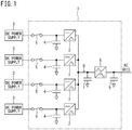
- FIG. 1 is a single-line connection diagram showing the schematic configuration of a power conversion device 1 provided between a plurality of DC power supplies 3 and an AC grid.
- the power conversion device 1 performs DC-to-AC power conversion, and includes a plurality of DC/DC converters 2 as boost converters, and a DC/AC converter 8 as an inverter circuit connected via an intermediate bus (DC bus) 6.
- DC bus intermediate bus
- FIG. 1 four pairs of DC power supplies 3 and DC/DC converters 2 are shown, but the "four pairs" are merely an example of the plurality.
- Each DC/DC converter 2 is provided between the corresponding DC power supply 3 and the intermediate bus 6.
- Each DC/DC converter 2 is provided, with a DC-side capacitor 4 and a switch 5 provided between the DC/DC converter 2 and the DC power supply 3.
- the switches 5 may be provided only for necessary DC power supplies 3.
- An intermediate capacitor 7 is connected to the intermediate bus 6.
- the DC/AC converter 8 is provided, via an AC-side capacitor 9, between the intermediate bus 6 and the AC grid.
- the DC power supply 3 is a photovoltaic panel or a storage battery, for example.
- the power conversion device 1 performs control according to a minimum switching conversion method, in which, while the voltage of each DC power supply 3 and the absolute value of the instantaneous voltage on the AC side are always compared with each other, the DC/DC converter 2 is caused to perform switching operation during only a period in which step-up operation is needed, and the DC/AC converter 8 is caused to perform switching operation during only a period in which step-down operation is needed.
- a period in which switching operation is stopped is provided to each of the DC/DC converter 2 and the DC/AC converter 8. If the stop period is provided, switching loss and reactor iron loss are reduced accordingly, so that conversion efficiency improves. It is noted that, in a case where the voltages of the DC power supplies 3 are different, the control is performed using the highest voltage value as a reference.
- FIG. 2 is an example of a circuit diagram of the power conversion device 1 shown in FIG. 1 .
- FIG. 2 For convenience of illustration, only two pairs of the four pairs of the DC power supplies 3 and the DC/DC converters 2 are shown, but the other two pairs are also connected in parallel to the intermediate bus 6 in the same manner.
- the power conversion device 1 includes a filter circuit 14, a control unit 20, and measurement sensors described later, as well as the DC-side capacitors 4, the DC/DC converters 2, the intermediate capacitor 7, and the DC/AC converter 8 described above.
- Each DC/DC converter 2 is a step-up chopper (step-down is also possible) including a DC reactor 11 and a pair of switching elements Q11, Q12.
- switching elements Q11, Q12 for example, IGBTs (Insulated Gate Bipolar Transistors) are used. Diodes d11, d12 are respectively connected in parallel to the switching elements Q11, Q12, in opposite-polarity directions. It is noted that, other than the above, FETs (Field Effect Transistors) may be used as the switching elements Q11, Q12.
- the DC/AC converter 8 includes four switching elements Q81, Q82, Q83, Q84 forming a full bridge.
- the switching elements Q81 to Q84 are, for example, FETs.
- the filter circuit 14 is composed of an AC reactor 13 and the AC-side capacitor 9, and prevents a high-frequency component contained in the AC output of the DC/AC converter 8 from leaking to the AC grid 17. It is noted that the AC grid 17 includes an AC load 15 and a commercial power grid 16.
- a voltage sensor 31 for detecting a voltage (V g ) between both ends of the DC-side capacitor 4; a current sensor 32 for detecting a current (I in ) flowing through each DC/DC converter 2; a voltage sensor 33 for detecting a voltage between both ends of the intermediate capacitor 7, i.e., a voltage (V o ) between two lines of the intermediate bus 6; a current sensor 34 for detecting a current (I inv ) flowing on the AC side of the DC/AC converter 8; and a voltage sensor 35 for detecting a voltage between both ends of the AC-side capacitor 9. Measurement output signals from all the sensors are sent to the control unit 20.
- the control unit 20 performs switching control for the DC/DC converters 2 and the DC/AC converter 8.
- the control unit 20 for example, includes a CPU and executes software (computer program) by a computer, thereby realizing necessary control functions.
- the software is stored in a storage device (not shown) of the control unit 20. It is noted that the control unit 20 may be configured from a circuit using only hardware not including a CPU.
- the left-hand side of expression (5) represents the sum of powers supplied from the plurality of DC/DC converters 2.
- the first term represents a power supplied to the DC/AC converter 8
- the second term represents a reactive power for the intermediate capacitor 7.
- g i and w i are allocation coefficients representing a ratio between an active power and a reactive power to be supplied from each DC/DC converter, and the sign of a power transmitted from the DC power supply to the AC side is defined as positive.
- the sign of g i is positive when photovoltaic generation or discharging of the storage battery is performed, and is negative when the storage battery is charged.
- a reactive power is allocated in proportion to an active power (active-power proportional allocation).
- active-power proportional allocation if the signs of g i are different from each other, i.e., photovoltaic generation and charging of the storage battery are performed at the same time, a reactive power that cancels a reactive power supplied from the photovoltaic panel is supplied from the storage battery, and thus more reactive powers than necessary are supplied from the respective DC/DC converters 2.
- proportional allocation may be performed such that the signs of reactive powers, i.e., phases of reactive currents, supplied from the respective DC/DC converters 2 coincide with each other.
- a part representing a voltage drop at the latter half of the denominator V g_i - (R in_i I* in_i (t) + L in_i (dI* in_i (t) / dt) contains a temporally-varying component, and therefore, strictly, the first term also contains a reactive current component.
- the varying component is as small as several V, and therefore ignored in the following analysis.
- a reactive power F(2 ⁇ t) flowing through the intermediate capacitor 7 is also small, and therefore ignored.
- expression (21) is obtained.
- expression (22) representing the effective value of a current flowing through the DC/DC converter 2 is obtained.
- the value of g i is 1/3 for the DC/DC converters 2 for photovoltaic panel, and is 0 for the DC/DC converter 2 for storage battery.
- w i is set at 1/6 for the DC/DC converters 2 for photovoltaic panel and 1/2 for the DC/DC converter 2 for storage battery, the value of the root part in expression (22) becomes ( ⁇ 2)/4 for both of the DC/DC converters 2 for photovoltaic panel and the DC/DC converters 2 for storage battery, and thus the powers are equalized.
- allocation may be performed with w i set so as to minimize expression (24).
- expression (24) since g i and w i are orthogonal to each other, allocation may be performed with w i set so as to minimize the second term shown below.
- ⁇ i 1 n w i V g _ i 2 R i
- the four DC/DC converters are referred to as a first DC/DC converter, a second DC/DC converter, a third DC/DC converter, and a fourth DC/DC converter.
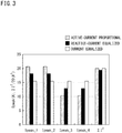
- FIG. 3 shows, as a bar graph, a result of peak currents Ipeak (Ipeak_1 to Ipeak_4) of the DC/DC converters and the sum of squares of the currents thereof, in a scale of (1/20) for convenience sake, in a case where the outputs of the first DC/DC converter and the second DC/DC converter are set at 2067 W and the outputs of the third DC/DC converter and the fourth DC/DC converter are set at 1033 W.
- a hatched bar indicates active-current proportional allocation
- a filled bar indicates reactive-current equalized allocation
- an outlined bar indicates current equalized allocation.
- the peak currents of the first DC/DC converter and the second DC/DC converter become maximum, i.e., 20.7 A.
- the peak currents of the first DC/DC converter and the second DC/DC converter are decreased to 17.1 A.
- the peak currents are further decreased to 15.5A.
- the value for reactive-current equalized allocation is the smallest. The difference thereof as compared to the sum of squares of currents for current equalized allocation is - 3.3%.
- FIG. 4 shows the peak values of currents flowing through the respective DC/DC converters and the sum of squares of currents of all the DC/DC converters in this case.
- the current peak values Ipeak_1, Ipeak_2, Ipeak_3 for the first to third DC/DC converters are 20.7 A for active-current proportional allocation, 18.1 A for reactive-current equalized allocation, and 15.5 A for current equalized allocation.
- active-current proportional allocation and current equalized allocation indicate the same value, and the value for reactive-current proportional allocation is smaller by 8.3% as compared to the other two allocations.
- the purchase price of a surplus power is further decreasing, and therefore there will be a less advantage in selling a power. Accordingly, without selling a surplus power of photovoltaic generation, the surplus power will be charged into the storage battery so as to be used for self-consumption. In this case, when photovoltaic generation is being performed, the storage battery is being charged, and therefore it is impossible to supply a reactive current from the DC/DC converter for storage battery. As a result, a reactive current is to be supplied from only the DC/DC converter for solar battery. However, as the self-consumption decreases and the proportion of charging of the storage battery increases, the output of the inverter decreases and therefore the necessary amount of reactive current also decreases.
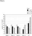
- FIG. 5 shows the current peak values of the respective DC/DC converters and the sum of squares of currents of all the DC/DC converters in a case where the outputs of the first to third DC/DC converters for solar battery are 2067 W and the output (for charging) of the fourth DC/DC converter for storage battery is changed to 0 W, - 2067 W, - 3100 W, and - 4133 W.
- Reactive currents are equally allocated for only the first to third DC/DC converters, without causing a reactive current to flow through the fourth DC/DC converter for storage battery.
- the current peak of the DC/DC converter for solar battery is 20.7 A at maximum, but as the charging amount for the storage battery increases, a reactive current to be borne decreases and therefore the current peak decreases.
- the current value becomes the same value of 20.7 A as the current peak value of the DC/DC converter for solar battery, when the charging amount is 4133 W.
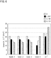
- FIG. 6 shows the current peak values of the respective DC/DC converters and the sum of squares of currents of all the DC/DC converters in this case.
- Reactive currents are equally allocated for only the first to third DC/DC converters for solar battery.
- a result when the output of the fourth DC/DC converter for storage battery is 0 W is the same as that in FIG. 5 .
- a reactive current to be borne by the fourth DC/DC converter for solar battery decreases.
- a reactive current to be borne by the fourth DC/DC converter for solar battery does not change, and as discharging of the storage battery increases, the active current decreases. The sum of squares of currents becomes maximum when discharging of the storage battery is at 4133 W.
- the DC/DC converter for solar battery In a case of performing charging or discharging of the storage battery when photovoltaic generation is being stopped, in order not to cause a reactive current to flow to the storage battery, the DC/DC converter for solar battery needs to supply a reactive current. If the DC/DC converter for solar battery is operated when photovoltaic generation is not being performed, the capacitor present on the solar battery side of the DC/DC converter is charged by a current flowing from the intermediate bus, and thus the voltage of the capacitor increases. At this time, a forward-direction voltage is applied from outside to each P-N junction of the solar battery, thereby establishing a conductive state, and thus the battery side of the DC/DC converter is short-circuited.
- FIG. 7 is a bar graph showing a result of this calculation.
- the first DC/DC converter is used for supplying a reactive current, while the second DC/DC converter and the third DC/DC converter are stopped. While the fourth DC/DC converter for storage battery supplies only an active current, the calculation has been performed for the cases where the output thereof is 2067 W, 3100 W, and 4133 W. When discharging of the storage battery is at 4133 W, the peak values of the active current flowing through the fourth DC/DC converter and the reactive current flowing through the first DC/DC converter are both 10.7 A.
- FIG. 7 shows a case of performing discharging of the storage battery, but also when charging is performed, the same result is obtained except that the direction of the current is changed.
Landscapes
- Engineering & Computer Science (AREA)
- Power Engineering (AREA)
- Inverter Devices (AREA)
- Control Of Electrical Variables (AREA)
Abstract
Description
- The present invention relates to a power conversion device and a control method therefor.
- This application claims priority on Japanese Patent Application No.
2015-205364 filed on October 19, 2015 - For converting the voltage of a DC power supply to a single-phase AC voltage, for example, a power conversion device including a boost converter (DC/DC converter) and an inverter circuit is used. In a traditional power conversion device, the voltage of a DC power supply is stepped up by a boost converter to a certain voltage higher than the peak voltage on the AC side, and thereafter, the resultant voltage is converted to an AC voltage by an inverter circuit. In this case, the boost converter and the inverter circuit always perform high-speed switching operations. Therefore, switching loss occurs in each switching element and iron loss occurs in a reactor. These losses become a factor for hampering improvement in conversion efficiency.
- Meanwhile, the following control is proposed: while the voltage of the DC power supply and the absolute value of the instantaneous voltage on the AC side are always compared with each other, the boost converter is caused to perform switching operation only during a period in which step-up operation is needed, and the inverter circuit is caused to perform switching operation only during a period in which a step-down operation is needed (see, for example, Patent Literature 1). In such control, the period in which the switching operation is stopped is provided to the boost converter and the inverter circuit. If the stop period is provided, switching loss and reactor iron loss are reduced accordingly, leading to improvement in conversion efficiency.
- Also in a power conversion device for which a plurality of DC power supplies are provided and which includes a plurality of DC/DC converters correspondingly for the respective DC power supplies, similarly, conversion efficiency can be improved (for example, see Patent Literature 2).
-
- PATENT LITERATURE 1: Japanese Laid-Open Patent Publication No.
2014-241714 - PATENT LITERATURE 2: Japanese Laid-Open Patent Publication No.
2014-241715 - The present invention is a power conversion device that performs power conversion via an intermediate bus between a plurality of DC power supplies and an AC grid, the power conversion device including: a plurality of DC/DC converters respectively provided between the intermediate bus and the plurality of DC power supplies; an intermediate capacitor connected to the intermediate bus; a DC/AC converter provided between the intermediate bus and the AC grid; and a control unit configured to control the plurality of DC/DC converters and the DC/AC converter, the control unit performing control of allocating, to the plurality of DC/DC converters, an active power to be outputted from the DC/AC converter, and allocating, to the plurality of DC/DC converters, a sum of reactive powers to be outputted from the DC/AC converter and the intermediate capacitor, using an allocation coefficient different from an allocation coefficient for the active power.
- A control method aspect is a control method for a power conversion device that includes: a plurality of DC/DC converters respectively provided between an intermediate bus and a plurality of DC power supplies; an intermediate capacitor connected to the intermediate bus; a DC/AC converter provided between the intermediate bus and an AC grid; and a control unit configured to control the plurality of DC/DC converters and the DC/AC converter, the power conversion device being configured to perform power conversion via the intermediate bus between the plurality of DC power supplies and the AC grid, the control method being executed by the control unit and including: allocating, to the plurality of DC/DC converters, an active power to be outputted from the DC/AC converter, and allocating, to the plurality of DC/DC converters, a sum of reactive powers to be outputted from the DC/AC converter and the intermediate capacitor, using an allocation coefficient different from an allocation coefficient for the active power.
-
-
FIG. 1 is a single-line connection diagram showing the schematic configuration of a power conversion device provided between a plurality of DC power supplies and an AC grid. -
FIG. 2 is an example of a circuit diagram of the power conversion device shown inFIG. 1 . -
FIG. 3 is a bar graph showing a result of peak currents Ipeak (Ipeak_1 to Ipeak_4) of DC/DC converters and the sum of squares of the currents thereof, in a scale of (1/20) for convenience sake, in a case where the outputs of a first DC/DC converter and a second DC/DC converter are set at 2067 W and the outputs of a third DC/DC converter and a fourth DC/DC converter are set at 1033 W. -
FIG. 4 is a bar graph showing the peak values of currents flowing through the respective DC/DC converters and the sum of squares of currents of all the DC/DC converters in a case where charging/discharging of the storage battery is stopped and the other three DC/DC converters for solar battery are operating at the maximum outputs. -
FIG. 5 is a bar graph showing the current peak values of the respective DC/DC converters and the sum of squares of currents of all the DC/DC converters in a case where the outputs of the first to third DC/DC converters for solar battery are 2067 W and the output (for charging) of the fourth DC/DC converter for storage battery is changed to 0 W, - 2067 W, - 3100 W, and - 4133 W. -
FIG. 6 is a bar graph showing the current peak values of the respective DC/DC converters and the sum of squares of currents of all the DC/DC converters in a case of performing discharging of the storage battery at the same time as photovoltaic generation. -
FIG. 7 is a bar graph showing a result of calculation of the current peak values and the sum of squares in a case where photovoltaic panels are paralleled-off and only one DC/DC converter supplies a reactive current when power generation is stopped. - In the power conversion devices of
Patent Literature Patent Literature 2, allocation of currents is performed. Expressions representing the gist of this current allocation are as follows. It is noted that, in the following, there is no meaning in difference of character font (upright/italic), and the same character represents the same value (the same applies hereinafter). - First, symbols are defined as follows.
- I*a: a command value for an output current from the power conversion device to the AC grid
- Ca: the capacitance of an AC-side capacitor
- Va: an AC grid voltage
- I*inv: a current command value for an inverter circuit at a stage before a current flows to the AC-side capacitor
- La: the inductance of an AC reactor
- V*inv: a voltage command value for the inverter circuit at a stage before passing through an AC reactor
- V*o: a command value for a voltage to arise on the intermediate bus (the greater one of the maximum value of V*g.i, and V*inv)
- Co: the capacitance of an intermediate capacitor
- V*g.i: a DC input voltage value (i is
numbers - I*g.i: a DC input current command value
- s: Laplace operator
- A notation "< >" indicates an average value of a value in the brackets.
- The part inside the parentheses on the right-hand side of the above expression (1) is a power outputted from the DC/DC converter, and contains an active power and a reactive power. In expression (2) obtained by deforming expression (1), a current command value I*in.i is obtained by allocating a power to be outputted from the DC/DC converter so as to be proportional to an active power I*g.i×V*g.i supplied from the DC power supply, and then dividing the resultant value by the voltage V*g.i of the DC power supply. That is, in this case, the active power and the reactive power to be outputted from the DC/DC converter are both allocated so as to be proportional to an active power outputted from the DC power supply.
- Here, for example, in a case where the DC power supply is a photovoltaic panel, the active power outputted from the DC/DC converter is controlled so as to achieve an optimum operation point at which the output of the photovoltaic panel is maximized.
- However, in the power conversion device of
Patent Literature 2, a more reactive power is allocated to the DC/DC converter to which a photovoltaic panel that outputs a greater active power is connected, and thus a current is likely to concentrate on a specific DC/DC converter, so that power loss occurring in this DC/DC converter increases. - In view of the above problem, an object of the present disclosure is to further reduce power loss in a power conversion device.
- The power conversion device and the control method therefor of the present disclosure can further reduce power loss.
- Summary of the embodiments of the present invention includes at least the following.
- (1) This is a power conversion device that performs power conversion via an intermediate bus between a plurality of DC power supplies and an AC grid, the power conversion device including: a plurality of DC/DC converters respectively provided between the intermediate bus and the plurality of DC power supplies; an intermediate capacitor connected to the intermediate bus; a DC/AC converter provided between the intermediate bus and the AC grid; and a control unit configured to control the plurality of DC/DC converters and the DC/AC converter, the control unit performing control of allocating, to the plurality of DC/DC converters, an active power to be outputted from the DC/AC converter, and allocating, to the plurality of DC/DC converters, a sum of reactive powers to be outputted from the DC/AC converter and the intermediate capacitor, using an allocation coefficient different from an allocation coefficient for the active power.
In the power conversion device configured as described above, it is possible to optimally allocate reactive powers using an allocation coefficient different from an allocation coefficient for an active power. Therefore, for example, by setting the allocation coefficient so as to equalize peak values of powers of the respective DC/DC converters, it becomes possible to perform such allocation as to minimize the peak values of currents flowing through the respective DC/DC converters. In addition, for example, focusing on power loss occurring in the DC/DC converters, it is also possible to set the allocation coefficient so as to minimize the power loss.
It is noted that, from the above, the control unit can also be expressed as follows, though this is also relevant to (2) below. That is, it can be recited that "the control unit performs control of allocating, to the plurality of DC/DC converters, an active power to be outputted from the DC/AC converter, and allocating, to the plurality of DC/DC converters, a sum of reactive powers to be outputted from the DC/AC converter and the intermediate capacitor, using an allocation coefficient different from an allocation coefficient for the active power, thereby equalizing peak values of powers of the DC/DC converters". - (2) In the power conversion device of (1), the control unit may perform control of allocating the sum of the reactive powers to the plurality of DC/DC converters so that peak values of powers or currents of the plurality of DC/DC converters are equalized.
In this case, it is possible to minimize the peak values of currents flowing through the respective DC/DC converters. - (3) In the power conversion device of (1), when maximum outputs of the plurality of DC/DC converters are the same as each other, the control unit may perform control of allocating the sum of the reactive powers to the plurality of DC/DC converters so that reactive powers or reactive currents of the plurality of DC/DC converters are equalized.
In this case, it is possible to minimize the peak values of currents flowing through the respective DC/DC converters. - (4) In the power conversion device of (1), the control unit may set the allocation coefficient for the reactive currents, in proportion to a square of an input voltage to each of the plurality of DC/DC converters.
In this case, it is possible to minimize power loss occurring in each DC/DC converter. - (5) In the power conversion device of any one of (1) to (4), the control unit may exclude, from a target of reactive power allocation, the DC/DC converter to which a storage battery is connected, among the plurality of DC/DC converters.
In this case, it is possible to prevent power loss from occurring due to a reactive current flowing through the storage battery. - (6) A control method aspect is a control method for a power conversion device that includes: a plurality of DC/DC converters respectively provided between an intermediate bus and a plurality of DC power supplies; an intermediate capacitor connected to the intermediate bus; a DC/AC converter provided between the intermediate bus and an AC grid; and a control unit configured to control the plurality of DC/DC converters and the DC/AC converter, the power conversion device being configured to perform power conversion via the intermediate bus between the plurality of DC power supplies and the AC grid, the control method being executed by the control unit and including: allocating, to the plurality of DC/DC converters, an active power to be outputted from the DC/AC converter, and allocating, to the plurality of DC/DC converters, a sum of reactive powers to be outputted from the DC/AC converter and the intermediate capacitor, using an allocation coefficient different from an allocation coefficient for the active power.
- In the control method for the power conversion device as described above, it is possible to optimally allocate reactive powers using an allocation coefficient different from an allocation coefficient for an active power. Therefore, for example, by setting the allocation coefficient so as to equalize peak values of powers of the respective DC/DC converters, it becomes possible to perform such allocation as to minimize the peak values of currents flowing through the respective DC/DC converters. In addition, for example, focusing on power loss occurring in the DC/DC converters, it is also possible to set the allocation coefficient so as to minimize the power loss.
- Hereinafter, the details of embodiments of the present invention will be described with reference to the drawings.
-
FIG. 1 is a single-line connection diagram showing the schematic configuration of apower conversion device 1 provided between a plurality ofDC power supplies 3 and an AC grid. InFIG. 1 , thepower conversion device 1 performs DC-to-AC power conversion, and includes a plurality of DC/DC converters 2 as boost converters, and a DC/AC converter 8 as an inverter circuit connected via an intermediate bus (DC bus) 6. In this example, four pairs ofDC power supplies 3 and DC/DC converters 2 are shown, but the "four pairs" are merely an example of the plurality. - Each DC/
DC converter 2 is provided between the correspondingDC power supply 3 and theintermediate bus 6. Each DC/DC converter 2 is provided, with a DC-side capacitor 4 and aswitch 5 provided between the DC/DC converter 2 and theDC power supply 3. Here, an example in which theswitches 5 are provided correspondingly for all theDC power supplies 3, is shown. However, theswitches 5 may be provided only for necessary DC power supplies 3. An intermediate capacitor 7 is connected to theintermediate bus 6. The DC/AC converter 8 is provided, via an AC-side capacitor 9, between theintermediate bus 6 and the AC grid. It is noted that theDC power supply 3 is a photovoltaic panel or a storage battery, for example. - The
power conversion device 1 performs control according to a minimum switching conversion method, in which, while the voltage of eachDC power supply 3 and the absolute value of the instantaneous voltage on the AC side are always compared with each other, the DC/DC converter 2 is caused to perform switching operation during only a period in which step-up operation is needed, and the DC/AC converter 8 is caused to perform switching operation during only a period in which step-down operation is needed. In such control, a period in which switching operation is stopped is provided to each of the DC/DC converter 2 and the DC/AC converter 8. If the stop period is provided, switching loss and reactor iron loss are reduced accordingly, so that conversion efficiency improves. It is noted that, in a case where the voltages of theDC power supplies 3 are different, the control is performed using the highest voltage value as a reference. -
FIG. 2 is an example of a circuit diagram of thepower conversion device 1 shown inFIG. 1 . For convenience of illustration, only two pairs of the four pairs of theDC power supplies 3 and the DC/DC converters 2 are shown, but the other two pairs are also connected in parallel to theintermediate bus 6 in the same manner. - The parts corresponding to those in
FIG. 1 are denoted by the same reference characters. InFIG. 2 , thepower conversion device 1 includes afilter circuit 14, acontrol unit 20, and measurement sensors described later, as well as the DC-side capacitors 4, the DC/DC converters 2, the intermediate capacitor 7, and the DC/AC converter 8 described above. - Each DC/
DC converter 2 is a step-up chopper (step-down is also possible) including aDC reactor 11 and a pair of switching elements Q11, Q12. As the switching elements Q11, Q12, for example, IGBTs (Insulated Gate Bipolar Transistors) are used. Diodes d11, d12 are respectively connected in parallel to the switching elements Q11, Q12, in opposite-polarity directions. It is noted that, other than the above, FETs (Field Effect Transistors) may be used as the switching elements Q11, Q12. - The DC/
AC converter 8 includes four switching elements Q81, Q82, Q83, Q84 forming a full bridge. The switching elements Q81 to Q84 are, for example, FETs. - The
filter circuit 14 is composed of anAC reactor 13 and the AC-side capacitor 9, and prevents a high-frequency component contained in the AC output of the DC/AC converter 8 from leaking to theAC grid 17. It is noted that theAC grid 17 includes anAC load 15 and acommercial power grid 16. - As the aforementioned sensors, provided are: a
voltage sensor 31 for detecting a voltage (Vg) between both ends of the DC-side capacitor 4; acurrent sensor 32 for detecting a current (Iin) flowing through each DC/DC converter 2; avoltage sensor 33 for detecting a voltage between both ends of the intermediate capacitor 7, i.e., a voltage (Vo) between two lines of theintermediate bus 6; acurrent sensor 34 for detecting a current (Iinv) flowing on the AC side of the DC/AC converter 8; and avoltage sensor 35 for detecting a voltage between both ends of the AC-side capacitor 9. Measurement output signals from all the sensors are sent to thecontrol unit 20. Thecontrol unit 20 performs switching control for the DC/DC converters 2 and the DC/AC converter 8. - The
control unit 20, for example, includes a CPU and executes software (computer program) by a computer, thereby realizing necessary control functions. The software is stored in a storage device (not shown) of thecontrol unit 20. It is noted that thecontrol unit 20 may be configured from a circuit using only hardware not including a CPU. - Next, the control theory of the
power conversion device 1 configured as described above will be described. First, various values will be defined as follows. -
- Va: an AC grid voltage detected by the
voltage sensor 35 - I*a: a command value for an AC current to flow to the
AC grid 17 - Iinv: an AC current detected by the
current sensor 34 - Ca: the capacitance of the AC-
side capacitor 9 - I*inv: a command value for a current to flow from the DC/
AC converter 8 to theAC reactor 13 - V*inv: a voltage command value for the AC side of the DC/
AC converter 8 - Rinv: a resistance component of the DC/
AC converter 8 - Linv: the inductance of the
AC reactor 13 - I*in: a command value for a current to flow to the
DC reactor 11 of the DC/DC converter 2 - Iin: a DC current detected by the
current sensor 32 - Co: the capacitance of the intermediate capacitor 7
- V*ο: a command value for a voltage to arise between both ends of the intermediate capacitor 7
- Vo: an intermediate voltage detected by the
voltage sensor 33 - Vg: a DC voltage detected by the
voltage sensor 31 - Rin: a resistance component of the DC/
DC converter 2 - Linv: the inductance of the
DC reactor 11 - An equation of the instantaneous power at the
intermediate bus 6 is represented by the following expression (5). It is noted that (t) indicates a function of time.
- The left-hand side of expression (5) represents the sum of powers supplied from the plurality of DC/
DC converters 2. On the right-hand side, the first term represents a power supplied to the DC/AC converter 8, and the second term represents a reactive power for the intermediate capacitor 7. - From here, expressions will be analyzed as follows.


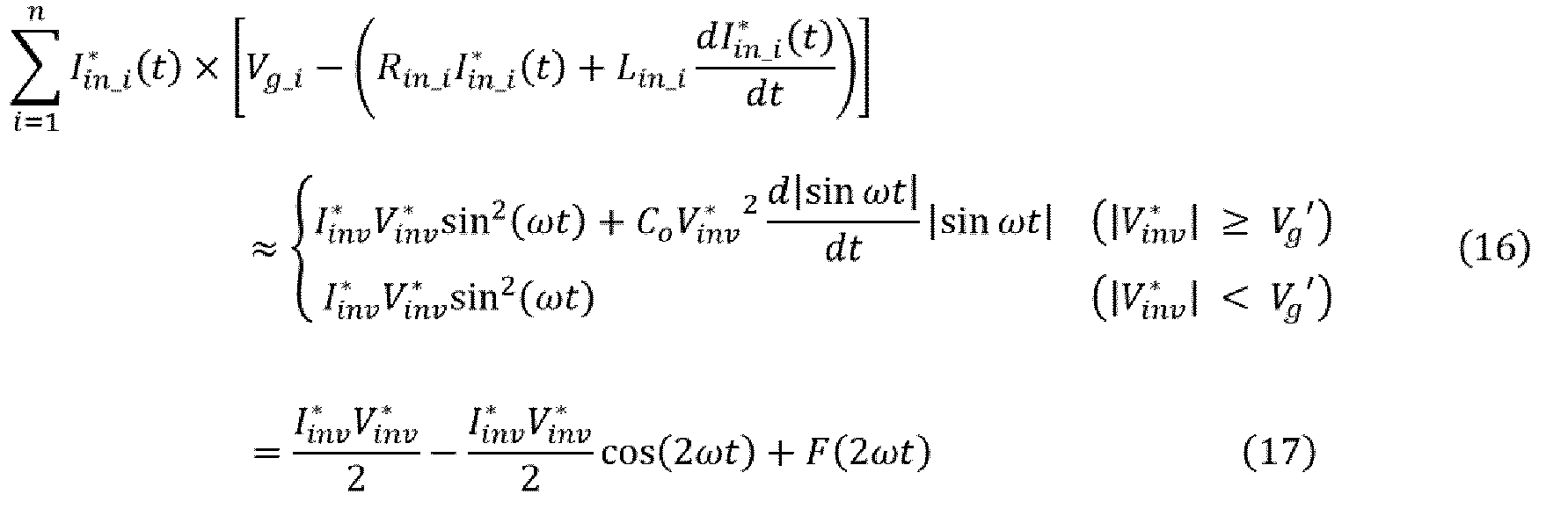


- As shown by expression (9) and expression (13), if I*inv(t) and V*inv(t) are approximated so that they can be represented as sine waves synchronized with each other, the right-hand side of expression (5) is arranged as shown by expression (17). Further, the right-hand side is rewritten in a form of linear combination so as to correspond to powers supplied from the respective DC/
DC converters 2, thereby obtaining expression (18). - Here, gi and wi are allocation coefficients representing a ratio between an active power and a reactive power to be supplied from each DC/DC converter, and the sign of a power transmitted from the DC power supply to the AC side is defined as positive. The sign of gi is positive when photovoltaic generation or discharging of the storage battery is performed, and is negative when the storage battery is charged.
- As shown by expression (19), when the power flow direction as a whole is from DC to AC, the following is satisfied.

- When the power flow direction as a whole is from AC to DC, the following is satisfied.


- Here, for reference, if, for example, gi = wi is satisfied, a reactive power is allocated in proportion to an active power (active-power proportional allocation). However, in a case of this allocation, if the signs of gi are different from each other, i.e., photovoltaic generation and charging of the storage battery are performed at the same time, a reactive power that cancels a reactive power supplied from the photovoltaic panel is supplied from the storage battery, and thus more reactive powers than necessary are supplied from the respective DC/
DC converters 2. In this case, with the absolute value of gi set to be equal to wi, proportional allocation may be performed such that the signs of reactive powers, i.e., phases of reactive currents, supplied from the respective DC/DC converters 2 coincide with each other. - On the other hand, if wi is determined so that the value of gi(I*inv·V*inv / 2) + wi{-(I*inv·V*inv / 2)cos(2ωt) + F(2ωt)} becomes constant, reactive powers are allocated so that powers supplied from the respective DC/
DC converters 2 are equalized (power equalized allocation). In this allocation method, more reactive power is allocated to the DC/DC converter 2 that has a smaller supply amount of active power. - In addition, similarly to the above method, a method of performing allocation so that the currents of expression (20) are equalized (current equalized allocation) is also conceivable. If the currents are equally allocated, the peak value of a current flowing through each DC/
DC converter 2 is minimized. Therefore, the current capacities of theDC reactor 11 and the switching elements Q11, Q12 can be minimized. - In expression (20), a part representing a voltage drop at the latter half of the denominator Vg_i - (Rin_iI*in_i(t) + Lin_i(dI*in_i(t) / dt) contains a temporally-varying component, and therefore, strictly, the first term also contains a reactive current component. However, as compared to the power supply voltage of about 200 V, the varying component is as small as several V, and therefore ignored in the following analysis. In addition, a reactive power F(2ωt) flowing through the intermediate capacitor 7 is also small, and therefore ignored. Thus, expression (21) is obtained. Further, by calculating the square root of mean square of expression (21), expression (22) representing the effective value of a current flowing through the DC/
DC converter 2 is obtained. - If wi is set so that (gi 2 + (wi 2/2))1/2 in expression (22) becomes constant, the power can be equally allocated. In addition, if wi is set so that (gi 2 + (wi 2/2))1/2 / Vg_i becomes constant, the current can be equally allocated.
- For example, in a case where three DC/
DC converters 2 connected to photovoltaic panels equally perform outputs and the storage battery is stopped, the value of gi is 1/3 for the DC/DC converters 2 for photovoltaic panel, and is 0 for the DC/DC converter 2 for storage battery. At this time, if wi is set at 1/6 for the DC/DC converters 2 for photovoltaic panel and 1/2 for the DC/DC converter 2 for storage battery, the value of the root part in expression (22) becomes (√2)/4 for both of the DC/DC converters 2 for photovoltaic panel and the DC/DC converters 2 for storage battery, and thus the powers are equalized.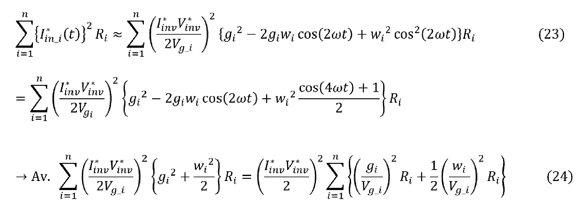


- On the other hand, in order to minimize power loss caused by the resistance of the DC/DC converter, allocation may be performed with wi set so as to minimize expression (24). In expression (24), since gi and wi are orthogonal to each other, allocation may be performed with wi set so as to minimize the second term shown below.

- In a case where all the DC/
DC converters 2 are the same and their resistance components Ri are equal to each other, power loss is minimized by performing allocation with wi set in accordance with expression (25). Further, in a case where all the voltages of the DC power supplies connected to the respective DC/DC converters 2 are the same, loss is minimized by simply allocating wi equally in accordance with the number of the DC/DC converters 2 as shown by expression (26). Therefore, unless all the values of gi are equal, the allocation setting for wi that minimizes the peak value of current does not coincide with the condition that minimizes power loss. - In the allocation methods for reactive currents described above, it is assumed that reactive currents are supplied from all the DC/
DC converters 2. In this case, a reactive current flows through the storage battery, and therefore there is a problem that loss due to the internal resistance of the storage battery increases. In the case of photovoltaic panel, since the output impedance is comparatively great, if a capacitor having a great capacitance is provided between the DC/DC converter 2 and the photovoltaic panel, a reactive current is absorbed by this capacitor, and thus a reactive current hardly flows through the photovoltaic panel. - However, in the case of storage battery, since the impedance thereof is small, even if a capacitor is provided between the storage battery and the DC/
DC converter 2, the effect thereof is small and a reactive current almost directly flows to the storage battery. Accordingly, it is preferable to allocate reactive currents using only the DC/DC converters 2 for photovoltaic panel while excluding the DC/DC converter 2 for storage battery. However, when charging/discharging of the storage battery is stopped, if aswitch 5 provided between the storage battery and the DC/DC converter 2 is opened, a current does not flow to the storage battery, and therefore a reactive current can be allocated also to the DC/DC converter 2 for storage battery. - Optimum allocation of reactive currents will be further discussed by showing specific examples, while, for the purpose of simplifying calculation, all the voltages of the DC power supplies are set at 200 V, and the voltage of the AC grid is set at 200 V (effective value).
- In a case where photovoltaic panels are connected to all the four DC/DC converters, the peak value of a current flowing through each DC/DC converter and the sum of squares of those currents have been calculated while the allocation method for reactive currents is changed. Hereinafter, the four DC/DC converters are referred to as a first DC/DC converter, a second DC/DC converter, a third DC/DC converter, and a fourth DC/DC converter.
-
FIG. 3 shows, as a bar graph, a result of peak currents Ipeak (Ipeak_1 to Ipeak_4) of the DC/DC converters and the sum of squares of the currents thereof, in a scale of (1/20) for convenience sake, in a case where the outputs of the first DC/DC converter and the second DC/DC converter are set at 2067 W and the outputs of the third DC/DC converter and the fourth DC/DC converter are set at 1033 W. In the bar graph, a hatched bar indicates active-current proportional allocation, a filled bar indicates reactive-current equalized allocation, and an outlined bar indicates current equalized allocation. - As shown in the graph, in the case of active-current proportional allocation, the peak currents of the first DC/DC converter and the second DC/DC converter become maximum, i.e., 20.7 A. In the case of reactive-current equalized allocation, the peak currents of the first DC/DC converter and the second DC/DC converter are decreased to 17.1 A. In the case of current equalized allocation, the peak currents are further decreased to 15.5A. As for the sum of squares of currents, the value for reactive-current equalized allocation is the smallest. The difference thereof as compared to the sum of squares of currents for current equalized allocation is - 3.3%.
- As in this example, if the maximum output is different among the DC/DC converters, it is also conceivable that current equalized allocation is employed to equalize the currents of all the DC/DC converters and elements having the same rating are used for the components such as the DC reactor and the switching elements. If the maximum outputs of all the DC/DC converters are the same, it is considered desirable to employ reactive-current equalized allocation to minimize loss.
- Next, a case where there are three (first to third) DC/DC converters for solar battery and one (fourth) DC/DC converter for storage battery will be described. First, a case where charging/discharging of the storage battery is stopped and the other three DC/DC converters for solar battery are operating at the maximum outputs, will be described. In this case, it is assumed that the storage battery is paralleled-off from the DC/DC converter, and the DC/DC converter for storage battery can supply only a reactive current.
FIG. 4 shows the peak values of currents flowing through the respective DC/DC converters and the sum of squares of currents of all the DC/DC converters in this case. - The current peak values Ipeak_1, Ipeak_2, Ipeak_3 for the first to third DC/DC converters are 20.7 A for active-current proportional allocation, 18.1 A for reactive-current equalized allocation, and 15.5 A for current equalized allocation. As for the sum of squares of the currents, active-current proportional allocation and current equalized allocation indicate the same value, and the value for reactive-current proportional allocation is smaller by 8.3% as compared to the other two allocations. Thus, when the photovoltaic panel is generating a power, if the storage battery is stopped and meanwhile a reactive current is supplied from the DC/DC converter for storage battery by reactive-current equalized allocation, conversion efficiency can be enhanced. Alternatively, if current equalized allocation is used, the efficiency does not change, but the peak value of a current flowing through the DC/DC converter for solar battery can be reduced and therefore the ratings of components such as the DC reactor can be reduced. Such methods are effective in a case of not performing so-called double power generation in which a surplus power of photovoltaic generation is sold and boosting-up by the storage battery is performed.
- From now on, the purchase price of a surplus power is further decreasing, and therefore there will be a less advantage in selling a power. Accordingly, without selling a surplus power of photovoltaic generation, the surplus power will be charged into the storage battery so as to be used for self-consumption. In this case, when photovoltaic generation is being performed, the storage battery is being charged, and therefore it is impossible to supply a reactive current from the DC/DC converter for storage battery. As a result, a reactive current is to be supplied from only the DC/DC converter for solar battery. However, as the self-consumption decreases and the proportion of charging of the storage battery increases, the output of the inverter decreases and therefore the necessary amount of reactive current also decreases.
-
FIG. 5 shows the current peak values of the respective DC/DC converters and the sum of squares of currents of all the DC/DC converters in a case where the outputs of the first to third DC/DC converters for solar battery are 2067 W and the output (for charging) of the fourth DC/DC converter for storage battery is changed to 0 W, - 2067 W, - 3100 W, and - 4133 W. Reactive currents are equally allocated for only the first to third DC/DC converters, without causing a reactive current to flow through the fourth DC/DC converter for storage battery. - When charging of the storage battery is zero, the current peak of the DC/DC converter for solar battery is 20.7 A at maximum, but as the charging amount for the storage battery increases, a reactive current to be borne decreases and therefore the current peak decreases. On the other hand, since a current flowing through the DC/DC converter for storage battery is only an active current, the current value becomes the same value of 20.7 A as the current peak value of the DC/DC converter for solar battery, when the charging amount is 4133 W.
- Therefore, as long as necessary cooling can be performed, it is possible to perform charging up to 4 kW using the same DC reactor and semiconductor devices as those used for the DC/DC converter for solar battery. In a home where nobody is likely to be present during the day so that power consumption is small, there is a large amount of surplus power in photovoltaic generation, and therefore it is desirable that the charging capacity is great. If the DC/DC converter for storage battery is caused to bear only an active current and thereby it becomes possible to supply more active current, the charging capacity can be increased accordingly, and this is advantageous for the purpose of self-consumption of surplus current.
- In a case where self-consumption is greater than power generation, discharging of the storage battery is performed at the same time as power generation.
FIG. 6 shows the current peak values of the respective DC/DC converters and the sum of squares of currents of all the DC/DC converters in this case. For the outputs of the first to third DC/DC converters for solar battery, a power obtained by subtracting the output of the fourth DC/DC converter for storage battery from the maximum output 6200 W of the power conversion device is equally allocated, while the output of the fourth DC/DC converter is changed to 0 W, 2067 W, 3100 W, and 4133 W. - Reactive currents are equally allocated for only the first to third DC/DC converters for solar battery. A result when the output of the fourth DC/DC converter for storage battery is 0 W is the same as that in
FIG. 5 . InFIG. 5 , as charging of the storage battery increases, a reactive current to be borne by the fourth DC/DC converter for solar battery decreases. However, inFIG. 6 , a reactive current to be borne by the fourth DC/DC converter for solar battery does not change, and as discharging of the storage battery increases, the active current decreases. The sum of squares of currents becomes maximum when discharging of the storage battery is at 4133 W. - In a case of performing charging or discharging of the storage battery when photovoltaic generation is being stopped, in order not to cause a reactive current to flow to the storage battery, the DC/DC converter for solar battery needs to supply a reactive current. If the DC/DC converter for solar battery is operated when photovoltaic generation is not being performed, the capacitor present on the solar battery side of the DC/DC converter is charged by a current flowing from the intermediate bus, and thus the voltage of the capacitor increases. At this time, a forward-direction voltage is applied from outside to each P-N junction of the solar battery, thereby establishing a conductive state, and thus the battery side of the DC/DC converter is short-circuited.
- In this state, it is impossible to supply a reactive power from the capacitor of the DC/DC converter for solar battery. Therefore, in order to supply a reactive current from the DC/DC converter when the solar battery is not generating power, it is necessary to parallel-off the photovoltaic panel by providing a
switch 5 that can be controlled to be opened/closed by thecontrol unit 20, between the solar battery and the DC/DC converter. For the purpose of suppressing cost increase as much as possible, only one DC/DC converter is used for supplying a reactive current when power generation is stopped. Under this condition, the current peak values and the sum of squares have been calculated.FIG. 7 is a bar graph showing a result of this calculation. - The first DC/DC converter is used for supplying a reactive current, while the second DC/DC converter and the third DC/DC converter are stopped. While the fourth DC/DC converter for storage battery supplies only an active current, the calculation has been performed for the cases where the output thereof is 2067 W, 3100 W, and 4133 W. When discharging of the storage battery is at 4133 W, the peak values of the active current flowing through the fourth DC/DC converter and the reactive current flowing through the first DC/DC converter are both 10.7 A.
FIG. 7 shows a case of performing discharging of the storage battery, but also when charging is performed, the same result is obtained except that the direction of the current is changed. - It is noted that the embodiments disclosed herein are merely illustrative in all aspects and should not be recognized as being restrictive. The scope of the present invention is defined by the scope of the claims, and is intended to include meaning equivalent to the scope of the claims and all modifications within the scope.
-
- 1 power conversion device
- 2 DC/DC converter
- 3 DC power supply
- 4 DC-side capacitor
- 5 switch
- 6 intermediate bus
- 7 intermediate capacitor
- 8 DC/AC converter
- 9 AC-side capacitor
- 11 DC reactor
- 13 AC reactor
- 14 filter circuit
- 15 AC load
- 16 commercial power grid
- 17 AC grid
- 20 control unit
- 31 voltage sensor
- 32 current sensor
- 33 voltage sensor
- 34 current sensor
- 35 voltage sensor
- Q11, Q12, Q81, Q82, Q83, Q84 switching element
- d11,d12 diode



Claims (7)
- A power conversion device that performs power conversion via an intermediate bus between a plurality of DC power supplies and an AC grid, the power conversion device comprising:a plurality of DC/DC converters respectively provided between the intermediate bus and the plurality of DC power supplies;an intermediate capacitor connected to the intermediate bus;a DC/AC converter provided between the intermediate bus and the AC grid; anda control unit configured to control the plurality of DC/DC converters and the DC/AC converter, the control unit performing control of allocating, to the plurality of DC/DC converters, an active power to be outputted from the DC/AC converter, and allocating, to the plurality of DC/DC converters, a sum of reactive powers to be outputted from the DC/AC converter and the intermediate capacitor, using an allocation coefficient different from an allocation coefficient for the active power.
- The power conversion device according to claim 1, wherein
the control unit performs control of allocating the sum of the reactive powers to the plurality of DC/DC converters so that peak values of powers or currents of the plurality of DC/DC converters are equalized. - The power conversion device according to claim 1, wherein
when maximum outputs of the plurality of DC/DC converters are the same as each other, the control unit performs control of allocating the sum of the reactive powers to the plurality of DC/DC converters so that reactive powers or reactive currents of the plurality of DC/DC converters are equalized. - The power conversion device according to claim 1, wherein
the control unit sets the allocation coefficient for the reactive currents, in proportion to a square of an input voltage to each of the plurality of DC/DC converters. - The power conversion device according to any one of claims 1 to 4, wherein
the control unit excludes, from a target of reactive power allocation, the DC/DC converter to which a storage battery is connected, among the plurality of DC/DC converters. - A control method for a power conversion device that includes: a plurality of DC/DC converters respectively provided between an intermediate bus and a plurality of DC power supplies; an intermediate capacitor connected to the intermediate bus; a DC/AC converter provided between the intermediate bus and an AC grid; and a control unit configured to control the plurality of DC/DC converters and the DC/AC converter, the power conversion device being configured to perform power conversion via the intermediate bus between the plurality of DC power supplies and the AC grid, the control method being executed by the control unit and comprising:
allocating, to the plurality of DC/DC converters, an active power to be outputted from the DC/AC converter, and allocating, to the plurality of DC/DC converters, a sum of reactive powers to be outputted from the DC/AC converter and the intermediate capacitor, using an allocation coefficient different from an allocation coefficient for the active power. - A power conversion device that performs power conversion via an intermediate bus between a plurality of DC power supplies and an AC grid, the power conversion device comprising:a plurality of DC/DC converters respectively provided between the intermediate bus and the plurality of DC power supplies;an intermediate capacitor connected to the intermediate bus;a DC/AC converter provided between the intermediate bus and the AC grid; anda control unit configured to control the plurality of DC/DC converters and the DC/AC converter, the control unit performing control of allocating, to the plurality of DC/DC converters, an active power to be outputted from the DC/AC converter, and allocating, to the plurality of DC/DC converters, a sum of reactive powers to be outputted from the DC/AC converter and the intermediate capacitor, using an allocation coefficient different from an allocation coefficient for the active power, thereby equalizing peak values of powers of the DC/DC converters.
Applications Claiming Priority (2)
| Application Number | Priority Date | Filing Date | Title |
|---|---|---|---|
| JP2015205364A JP6536346B2 (en) | 2015-10-19 | 2015-10-19 | Power converter and control method thereof |
| PCT/JP2016/069818 WO2017068815A1 (en) | 2015-10-19 | 2016-07-04 | Power conversion device and control method thereof |
Publications (2)
| Publication Number | Publication Date |
|---|---|
| EP3367551A1 true EP3367551A1 (en) | 2018-08-29 |
| EP3367551A4 EP3367551A4 (en) | 2019-05-15 |
Family
ID=58556971
Family Applications (1)
| Application Number | Title | Priority Date | Filing Date |
|---|---|---|---|
| EP16857133.9A Ceased EP3367551A4 (en) | 2015-10-19 | 2016-07-04 | POWER CONVERTING DEVICE AND CONTROL METHOD THEREOF |
Country Status (8)
| Country | Link |
|---|---|
| US (1) | US20180262012A1 (en) |
| EP (1) | EP3367551A4 (en) |
| JP (1) | JP6536346B2 (en) |
| KR (1) | KR102549275B1 (en) |
| CN (1) | CN108207118B (en) |
| AU (1) | AU2016342806B2 (en) |
| TW (1) | TWI752921B (en) |
| WO (1) | WO2017068815A1 (en) |
Families Citing this family (4)
| Publication number | Priority date | Publication date | Assignee | Title |
|---|---|---|---|---|
| KR102488002B1 (en) * | 2018-04-05 | 2023-01-13 | 한국전자통신연구원 | Power conversion system and operating method thereof |
| CN113228494B (en) * | 2019-01-22 | 2024-05-14 | 住友电气工业株式会社 | Power conversion device and control method thereof |
| JP2020145819A (en) * | 2019-03-05 | 2020-09-10 | オムロン株式会社 | Power conditioner |
| CN115146744B (en) * | 2022-09-01 | 2022-12-06 | 安徽南瑞中天电力电子有限公司 | Electric energy meter load real-time identification method and system integrating time characteristics |
Family Cites Families (26)
| Publication number | Priority date | Publication date | Assignee | Title |
|---|---|---|---|---|
| JP4566658B2 (en) * | 2004-08-24 | 2010-10-20 | パナソニックエコシステムズ株式会社 | Power supply |
| US9112379B2 (en) * | 2006-12-06 | 2015-08-18 | Solaredge Technologies Ltd. | Pairing of components in a direct current distributed power generation system |
| EP2104200B1 (en) * | 2008-03-22 | 2019-02-27 | SMA Solar Technology AG | Method for controlling a multi-string inverter for photovoltaic systems |
| DK2363947T3 (en) * | 2010-03-03 | 2012-08-06 | Sma Solar Technology Ag | Inverters with multi-power electrical system |
| US9362815B2 (en) * | 2010-10-25 | 2016-06-07 | Bloom Energy Corporation | Input-parallel/output-parallel inverter assembly control device and method |
| JP2014509824A (en) * | 2011-03-16 | 2014-04-21 | エスエムエー ソーラー テクノロジー アーゲー | Grid-connected inverter, inverter device, and method for operating the inverter device |
| US9124136B1 (en) * | 2011-06-10 | 2015-09-01 | The Florida State University Research Foundation, Inc. | System and method for single-phase, single-stage grid-interactive inverter |
| US20120319489A1 (en) * | 2011-06-15 | 2012-12-20 | Mccaslin Shawn R | Power Shuffling Solar String Equalization System |
| US9099938B2 (en) * | 2011-12-16 | 2015-08-04 | Empower Micro Systems | Bi-directional energy converter with multiple DC sources |
| WO2013121618A1 (en) * | 2012-02-13 | 2013-08-22 | 三菱電機株式会社 | Power conversion device |
| US20130300196A1 (en) * | 2012-05-09 | 2013-11-14 | Dynapower Company, Llc | Multi-port inverter/converter system for dynamic micro-grid applications |
| IN2015DN01650A (en) * | 2012-09-03 | 2015-07-03 | Vestas Wind Sys As | |
| JP5940946B2 (en) * | 2012-09-20 | 2016-06-29 | 京セラ株式会社 | Power conditioner and control method thereof |
| US9685887B2 (en) * | 2012-10-12 | 2017-06-20 | Younicos Inc. | Controlling power conversion systems |
| JP2014099986A (en) * | 2012-11-14 | 2014-05-29 | Toshiba Corp | Composite power storage system |
| EP2957014B1 (en) * | 2013-02-14 | 2016-12-07 | ABB Schweiz AG | Method of controlling a solar power plant, a power conversion system, a dc/ac inverter and a solar power plant |
| US9898018B2 (en) * | 2013-03-14 | 2018-02-20 | Arda Power Inc. | Power clipping method and system |
| JP6267449B2 (en) | 2013-03-15 | 2018-01-24 | 東京エレクトロン株式会社 | Organic device manufacturing method and organic device manufacturing apparatus |
| CN104969139B (en) * | 2013-03-20 | 2016-10-05 | 富士电机株式会社 | The Sun can generate system |
| JP5618022B1 (en) | 2013-06-11 | 2014-11-05 | 住友電気工業株式会社 | Inverter device |
| JP5618023B1 (en) * | 2013-06-11 | 2014-11-05 | 住友電気工業株式会社 | Inverter device |
| US20150015072A1 (en) * | 2013-07-12 | 2015-01-15 | Infineon Technologies Austria Ag | Power Converter Circuit and Method |
| CN104753080A (en) * | 2013-12-30 | 2015-07-01 | 长沙理工大学 | Single-phase photovoltaic power supply grid-connected inverter hybrid automata control method |
| CN104868764B (en) * | 2014-02-26 | 2017-08-04 | 全汉企业股份有限公司 | Inverter and power supply conversion method thereof |
| JP2015180125A (en) * | 2014-03-18 | 2015-10-08 | 株式会社東芝 | Control apparatus, power conversion equipment, and control system |
| US10008854B2 (en) * | 2015-02-19 | 2018-06-26 | Enphase Energy, Inc. | Method and apparatus for time-domain droop control with integrated phasor current control |
-
2015
- 2015-10-19 JP JP2015205364A patent/JP6536346B2/en active Active
-
2016
- 2016-07-04 EP EP16857133.9A patent/EP3367551A4/en not_active Ceased
- 2016-07-04 US US15/762,155 patent/US20180262012A1/en not_active Abandoned
- 2016-07-04 CN CN201680059425.7A patent/CN108207118B/en not_active Expired - Fee Related
- 2016-07-04 WO PCT/JP2016/069818 patent/WO2017068815A1/en not_active Ceased
- 2016-07-04 KR KR1020187010343A patent/KR102549275B1/en active Active
- 2016-07-04 AU AU2016342806A patent/AU2016342806B2/en not_active Ceased
- 2016-10-17 TW TW105133439A patent/TWI752921B/en not_active IP Right Cessation
Also Published As
| Publication number | Publication date |
|---|---|
| CN108207118A (en) | 2018-06-26 |
| TW201715813A (en) | 2017-05-01 |
| KR20180072683A (en) | 2018-06-29 |
| TWI752921B (en) | 2022-01-21 |
| AU2016342806A1 (en) | 2018-03-29 |
| JP2017079509A (en) | 2017-04-27 |
| EP3367551A4 (en) | 2019-05-15 |
| AU2016342806B2 (en) | 2020-10-08 |
| WO2017068815A1 (en) | 2017-04-27 |
| KR102549275B1 (en) | 2023-06-28 |
| US20180262012A1 (en) | 2018-09-13 |
| CN108207118B (en) | 2021-01-12 |
| JP6536346B2 (en) | 2019-07-03 |
Similar Documents
| Publication | Publication Date | Title |
|---|---|---|
| US9966777B2 (en) | Modular multilevel converter for hybrid energy storage | |
| EP3648332B1 (en) | Direct power converter control device | |
| EP3104515B1 (en) | Power conversion device | |
| EP3051684A1 (en) | Control method for direct power conversion device | |
| EP3093975B1 (en) | Power conversion system | |
| EP3057223B1 (en) | Control method for direct power conversion device | |
| US10284113B2 (en) | Power conversion device performing DC/AC power conversion via intermediate bus, and control method thereof | |
| US20180262012A1 (en) | Power conversion device and control method thereof | |
| EP3188356A1 (en) | Power conversion device | |
| Sangdehi et al. | A novel bidirectional DC/AC stacked matrix converter design for electrified vehicle applications | |
| CN104300817B (en) | The control method of T-shaped three level SVPWM in energy conversion system | |
| Ayhan et al. | Analysis and characterization of DC bus ripple current of two-level inverters using the equivalent centered harmonic approach | |
| Jakka et al. | A triple port active bridge converter based multi-fed power electronic transformer | |
| JP2019075844A (en) | Power conversion device | |
| Serban et al. | Active power decoupling circuit for a single-phase battery energy storage system dedicated to autonomous microgrids | |
| CN103872683B (en) | Compensation device used for eliminating second harmonic pulsation in inverter and electrical power system | |
| Ahmad et al. | Experimental investigation and performance evaluation of an asymmetrical Eleven-Level Multilevel Inverter (ELMLI) with reduced switching count and voltage stress | |
| JP6623845B2 (en) | Power conversion system and power control method | |
| Kirchner et al. | Design of a cascaded hybrid multilevel converter for traction application | |
| EP3940944A1 (en) | Control device for direct power converter | |
| Agarwal et al. | Harmonic mitigation using multipulse voltage source converter-based HVDC system |
Legal Events
| Date | Code | Title | Description |
|---|---|---|---|
| STAA | Information on the status of an ep patent application or granted ep patent |
Free format text: STATUS: THE INTERNATIONAL PUBLICATION HAS BEEN MADE |
|
| PUAI | Public reference made under article 153(3) epc to a published international application that has entered the european phase |
Free format text: ORIGINAL CODE: 0009012 |
|
| STAA | Information on the status of an ep patent application or granted ep patent |
Free format text: STATUS: REQUEST FOR EXAMINATION WAS MADE |
|
| 17P | Request for examination filed |
Effective date: 20180306 |
|
| AK | Designated contracting states |
Kind code of ref document: A1 Designated state(s): AL AT BE BG CH CY CZ DE DK EE ES FI FR GB GR HR HU IE IS IT LI LT LU LV MC MK MT NL NO PL PT RO RS SE SI SK SM TR |
|
| AX | Request for extension of the european patent |
Extension state: BA ME |
|
| DAV | Request for validation of the european patent (deleted) | ||
| DAX | Request for extension of the european patent (deleted) | ||
| A4 | Supplementary search report drawn up and despatched |
Effective date: 20190415 |
|
| RIC1 | Information provided on ipc code assigned before grant |
Ipc: H02J 3/38 20060101ALI20190409BHEP Ipc: H02M 7/48 20070101AFI20190409BHEP Ipc: H02J 3/46 20060101ALI20190409BHEP Ipc: H02J 3/18 20060101ALI20190409BHEP |
|
| REG | Reference to a national code |
Ref country code: DE Ref legal event code: R003 |
|
| STAA | Information on the status of an ep patent application or granted ep patent |
Free format text: STATUS: THE APPLICATION HAS BEEN REFUSED |
|
| 18R | Application refused |
Effective date: 20201026 |