EP3367456A1 - Organic light-emitting device - Google Patents
Organic light-emitting device Download PDFInfo
- Publication number
- EP3367456A1 EP3367456A1 EP18158782.5A EP18158782A EP3367456A1 EP 3367456 A1 EP3367456 A1 EP 3367456A1 EP 18158782 A EP18158782 A EP 18158782A EP 3367456 A1 EP3367456 A1 EP 3367456A1
- Authority
- EP
- European Patent Office
- Prior art keywords
- group
- alkyl
- phenyl
- pyridinyl
- triazinyl
- Prior art date
- Legal status (The legal status is an assumption and is not a legal conclusion. Google has not performed a legal analysis and makes no representation as to the accuracy of the status listed.)
- Granted
Links
- 0 *1c(cccc2)c2-c2ccccc2C1c(cc1)cc(c2c3)c1[s]c2ccc3-[n]1c2ccccc2c2c1cccc2 Chemical compound *1c(cccc2)c2-c2ccccc2C1c(cc1)cc(c2c3)c1[s]c2ccc3-[n]1c2ccccc2c2c1cccc2 0.000 description 14
- QGUOGGDENOCSAR-UHFFFAOYSA-N C(C1)C=CC=C1[n]1c(ccc(N(c(cc2)ccc2-c(cc2)ccc2N(c(cc2c3c4cccc3)ccc2[n]4-c2ccccc2)c2cccc(-c3ccccc3)c2)c2cc(-c3ccccc3)ccc2)c2)c2c2ccccc12 Chemical compound C(C1)C=CC=C1[n]1c(ccc(N(c(cc2)ccc2-c(cc2)ccc2N(c(cc2c3c4cccc3)ccc2[n]4-c2ccccc2)c2cccc(-c3ccccc3)c2)c2cc(-c3ccccc3)ccc2)c2)c2c2ccccc12 QGUOGGDENOCSAR-UHFFFAOYSA-N 0.000 description 1
- BFSNZVXXSIVOLD-UHFFFAOYSA-N C(C1)C=Cc(c2c3ccc(N(c4ccccc4)c4ccccc4)c2)c1[n]3-c(cc1)ccc1-c1cc(-c2ccccc2)nc(-c2ccccc2)n1 Chemical compound C(C1)C=Cc(c2c3ccc(N(c4ccccc4)c4ccccc4)c2)c1[n]3-c(cc1)ccc1-c1cc(-c2ccccc2)nc(-c2ccccc2)n1 BFSNZVXXSIVOLD-UHFFFAOYSA-N 0.000 description 1
- ZGOBAOUQMPLRSI-UHFFFAOYSA-N CC(C1)C(c2nnc(-c(cc3)ccc3-c3ccccc3)[n]2-c2ccccc2)=CC=C1C(C)(C)C Chemical compound CC(C1)C(c2nnc(-c(cc3)ccc3-c3ccccc3)[n]2-c2ccccc2)=CC=C1C(C)(C)C ZGOBAOUQMPLRSI-UHFFFAOYSA-N 0.000 description 1
- GPPPQQUBLDVVCM-UHFFFAOYSA-N CC1(C)C(C=CCC2)=C2N(c(cc2)ccc2S(c(cc2)ccc2-[n]2c3ccccc3c3c2cccc3)(OC)=O)c2c1cccc2 Chemical compound CC1(C)C(C=CCC2)=C2N(c(cc2)ccc2S(c(cc2)ccc2-[n]2c3ccccc3c3c2cccc3)(OC)=O)c2c1cccc2 GPPPQQUBLDVVCM-UHFFFAOYSA-N 0.000 description 1
- NHARWQZRUAFVDU-UHFFFAOYSA-N CC1C([n](c2c3cccc2)c(cc2)c3c3c2c2ccccc2[n]3-c(cc2)ccc2-c2nc(-c3ccccc3)nc(-c3ccccc3)n2)=CC=CC1 Chemical compound CC1C([n](c2c3cccc2)c(cc2)c3c3c2c2ccccc2[n]3-c(cc2)ccc2-c2nc(-c3ccccc3)nc(-c3ccccc3)n2)=CC=CC1 NHARWQZRUAFVDU-UHFFFAOYSA-N 0.000 description 1
- BKKVUAUDJSYDCK-UHFFFAOYSA-N Fc(cc1)ccc1-[n]1c(ccc(N(c2ccccc2)c(cc2)ccc2-c(cc2)ccc2N(c2ccccc2)c(cc2c3ccccc33)ccc2[n]3-c(cc2)ccc2F)c2)c2c2ccccc12 Chemical compound Fc(cc1)ccc1-[n]1c(ccc(N(c2ccccc2)c(cc2)ccc2-c(cc2)ccc2N(c2ccccc2)c(cc2c3ccccc33)ccc2[n]3-c(cc2)ccc2F)c2)c2c2ccccc12 BKKVUAUDJSYDCK-UHFFFAOYSA-N 0.000 description 1
- VIHBOYVXGPKCLV-UHFFFAOYSA-N c(cc1)cc(c2c3cccc2)c1[n]3-c1cccc(-c2cc(-c(cc3)cc4c3[o]c3ccccc43)ccc2)c1 Chemical compound c(cc1)cc(c2c3cccc2)c1[n]3-c1cccc(-c2cc(-c(cc3)cc4c3[o]c3ccccc43)ccc2)c1 VIHBOYVXGPKCLV-UHFFFAOYSA-N 0.000 description 1
- HXPARCXOHJXWFN-UHFFFAOYSA-N c(cc1)ccc1-[n]1c(ccc(N(c(cc2)ccc2-c(cc2)ccc2N(c(cc2c3c4cccc3)ccc2[n]4-c2ccccc2)c2cccc3c2cccc3)c2cccc3ccccc23)c2)c2c2ccccc12 Chemical compound c(cc1)ccc1-[n]1c(ccc(N(c(cc2)ccc2-c(cc2)ccc2N(c(cc2c3c4cccc3)ccc2[n]4-c2ccccc2)c2cccc3c2cccc3)c2cccc3ccccc23)c2)c2c2ccccc12 HXPARCXOHJXWFN-UHFFFAOYSA-N 0.000 description 1
- AEABXZMGEOGKKE-UHFFFAOYSA-N c(cc1)ccc1-c(cc1)ccc1N(c(cc1)ccc1-c(cc1)ccc1N(c(cc1)ccc1-c1ccccc1)c(cc1c2ccccc22)ccc1[n]2-c1ccccc1)c(cc1)cc(c2ccccc22)c1[n]2-c1ccccc1 Chemical compound c(cc1)ccc1-c(cc1)ccc1N(c(cc1)ccc1-c(cc1)ccc1N(c(cc1)ccc1-c1ccccc1)c(cc1c2ccccc22)ccc1[n]2-c1ccccc1)c(cc1)cc(c2ccccc22)c1[n]2-c1ccccc1 AEABXZMGEOGKKE-UHFFFAOYSA-N 0.000 description 1
- IAZGPRGNVWBUFR-UHFFFAOYSA-N c(cc1)ccc1-c1cccc(-[n]2c(c3c(cc4)c(cccc5)c5[n]3-c3cc(-c5ccccc5)ccc3)c4c3c2cccc3)c1 Chemical compound c(cc1)ccc1-c1cccc(-[n]2c(c3c(cc4)c(cccc5)c5[n]3-c3cc(-c5ccccc5)ccc3)c4c3c2cccc3)c1 IAZGPRGNVWBUFR-UHFFFAOYSA-N 0.000 description 1
- PZCNFFIQAPXYBP-UHFFFAOYSA-N c(cc1)ccc1-c1nc(-c2ccccc2)nc(-c(cc2)ccc2-[n](c(cccc2)c2c2c3)c2ccc3N(c2ccccc2)c2ccccc2)c1 Chemical compound c(cc1)ccc1-c1nc(-c2ccccc2)nc(-c(cc2)ccc2-[n](c(cccc2)c2c2c3)c2ccc3N(c2ccccc2)c2ccccc2)c1 PZCNFFIQAPXYBP-UHFFFAOYSA-N 0.000 description 1
- AOQKGYRILLEVJV-UHFFFAOYSA-N c(cc1)ccc1-c1nnc(-c2ccccc2)[n]1-c1c(cccc2)c2ccc1 Chemical compound c(cc1)ccc1-c1nnc(-c2ccccc2)[n]1-c1c(cccc2)c2ccc1 AOQKGYRILLEVJV-UHFFFAOYSA-N 0.000 description 1
Images




Classifications
-
- H—ELECTRICITY
- H10—SEMICONDUCTOR DEVICES; ELECTRIC SOLID-STATE DEVICES NOT OTHERWISE PROVIDED FOR
- H10K—ORGANIC ELECTRIC SOLID-STATE DEVICES
- H10K85/00—Organic materials used in the body or electrodes of devices covered by this subclass
- H10K85/60—Organic compounds having low molecular weight
- H10K85/649—Aromatic compounds comprising a hetero atom
- H10K85/657—Polycyclic condensed heteroaromatic hydrocarbons
- H10K85/6572—Polycyclic condensed heteroaromatic hydrocarbons comprising only nitrogen in the heteroaromatic polycondensed ring system, e.g. phenanthroline or carbazole
-
- C—CHEMISTRY; METALLURGY
- C09—DYES; PAINTS; POLISHES; NATURAL RESINS; ADHESIVES; COMPOSITIONS NOT OTHERWISE PROVIDED FOR; APPLICATIONS OF MATERIALS NOT OTHERWISE PROVIDED FOR
- C09K—MATERIALS FOR MISCELLANEOUS APPLICATIONS, NOT PROVIDED FOR ELSEWHERE
- C09K11/00—Luminescent materials, e.g. electroluminescent or chemiluminescent
- C09K11/06—Luminescent materials, e.g. electroluminescent or chemiluminescent containing organic luminescent materials
-
- H—ELECTRICITY
- H10—SEMICONDUCTOR DEVICES; ELECTRIC SOLID-STATE DEVICES NOT OTHERWISE PROVIDED FOR
- H10K—ORGANIC ELECTRIC SOLID-STATE DEVICES
- H10K50/00—Organic light-emitting devices
- H10K50/10—OLEDs or polymer light-emitting diodes [PLED]
- H10K50/11—OLEDs or polymer light-emitting diodes [PLED] characterised by the electroluminescent [EL] layers
-
- H—ELECTRICITY
- H10—SEMICONDUCTOR DEVICES; ELECTRIC SOLID-STATE DEVICES NOT OTHERWISE PROVIDED FOR
- H10K—ORGANIC ELECTRIC SOLID-STATE DEVICES
- H10K50/00—Organic light-emitting devices
- H10K50/10—OLEDs or polymer light-emitting diodes [PLED]
- H10K50/11—OLEDs or polymer light-emitting diodes [PLED] characterised by the electroluminescent [EL] layers
- H10K50/12—OLEDs or polymer light-emitting diodes [PLED] characterised by the electroluminescent [EL] layers comprising dopants
-
- H—ELECTRICITY
- H10—SEMICONDUCTOR DEVICES; ELECTRIC SOLID-STATE DEVICES NOT OTHERWISE PROVIDED FOR
- H10K—ORGANIC ELECTRIC SOLID-STATE DEVICES
- H10K50/00—Organic light-emitting devices
- H10K50/10—OLEDs or polymer light-emitting diodes [PLED]
- H10K50/14—Carrier transporting layers
- H10K50/15—Hole transporting layers
-
- H—ELECTRICITY
- H10—SEMICONDUCTOR DEVICES; ELECTRIC SOLID-STATE DEVICES NOT OTHERWISE PROVIDED FOR
- H10K—ORGANIC ELECTRIC SOLID-STATE DEVICES
- H10K50/00—Organic light-emitting devices
- H10K50/10—OLEDs or polymer light-emitting diodes [PLED]
- H10K50/14—Carrier transporting layers
- H10K50/16—Electron transporting layers
- H10K50/166—Electron transporting layers comprising a multilayered structure
-
- H—ELECTRICITY
- H10—SEMICONDUCTOR DEVICES; ELECTRIC SOLID-STATE DEVICES NOT OTHERWISE PROVIDED FOR
- H10K—ORGANIC ELECTRIC SOLID-STATE DEVICES
- H10K50/00—Organic light-emitting devices
- H10K50/10—OLEDs or polymer light-emitting diodes [PLED]
- H10K50/17—Carrier injection layers
- H10K50/171—Electron injection layers
-
- H—ELECTRICITY
- H10—SEMICONDUCTOR DEVICES; ELECTRIC SOLID-STATE DEVICES NOT OTHERWISE PROVIDED FOR
- H10K—ORGANIC ELECTRIC SOLID-STATE DEVICES
- H10K50/00—Organic light-emitting devices
- H10K50/80—Constructional details
- H10K50/805—Electrodes
-
- H—ELECTRICITY
- H10—SEMICONDUCTOR DEVICES; ELECTRIC SOLID-STATE DEVICES NOT OTHERWISE PROVIDED FOR
- H10K—ORGANIC ELECTRIC SOLID-STATE DEVICES
- H10K71/00—Manufacture or treatment specially adapted for the organic devices covered by this subclass
-
- H—ELECTRICITY
- H10—SEMICONDUCTOR DEVICES; ELECTRIC SOLID-STATE DEVICES NOT OTHERWISE PROVIDED FOR
- H10K—ORGANIC ELECTRIC SOLID-STATE DEVICES
- H10K85/00—Organic materials used in the body or electrodes of devices covered by this subclass
- H10K85/40—Organosilicon compounds, e.g. TIPS pentacene
-
- H—ELECTRICITY
- H10—SEMICONDUCTOR DEVICES; ELECTRIC SOLID-STATE DEVICES NOT OTHERWISE PROVIDED FOR
- H10K—ORGANIC ELECTRIC SOLID-STATE DEVICES
- H10K85/00—Organic materials used in the body or electrodes of devices covered by this subclass
- H10K85/60—Organic compounds having low molecular weight
-
- H—ELECTRICITY
- H10—SEMICONDUCTOR DEVICES; ELECTRIC SOLID-STATE DEVICES NOT OTHERWISE PROVIDED FOR
- H10K—ORGANIC ELECTRIC SOLID-STATE DEVICES
- H10K85/00—Organic materials used in the body or electrodes of devices covered by this subclass
- H10K85/60—Organic compounds having low molecular weight
- H10K85/631—Amine compounds having at least two aryl rest on at least one amine-nitrogen atom, e.g. triphenylamine
- H10K85/636—Amine compounds having at least two aryl rest on at least one amine-nitrogen atom, e.g. triphenylamine comprising heteroaromatic hydrocarbons as substituents on the nitrogen atom
-
- H—ELECTRICITY
- H10—SEMICONDUCTOR DEVICES; ELECTRIC SOLID-STATE DEVICES NOT OTHERWISE PROVIDED FOR
- H10K—ORGANIC ELECTRIC SOLID-STATE DEVICES
- H10K85/00—Organic materials used in the body or electrodes of devices covered by this subclass
- H10K85/60—Organic compounds having low molecular weight
- H10K85/649—Aromatic compounds comprising a hetero atom
- H10K85/654—Aromatic compounds comprising a hetero atom comprising only nitrogen as heteroatom
-
- H—ELECTRICITY
- H10—SEMICONDUCTOR DEVICES; ELECTRIC SOLID-STATE DEVICES NOT OTHERWISE PROVIDED FOR
- H10K—ORGANIC ELECTRIC SOLID-STATE DEVICES
- H10K85/00—Organic materials used in the body or electrodes of devices covered by this subclass
- H10K85/60—Organic compounds having low molecular weight
- H10K85/649—Aromatic compounds comprising a hetero atom
- H10K85/657—Polycyclic condensed heteroaromatic hydrocarbons
-
- H—ELECTRICITY
- H10—SEMICONDUCTOR DEVICES; ELECTRIC SOLID-STATE DEVICES NOT OTHERWISE PROVIDED FOR
- H10K—ORGANIC ELECTRIC SOLID-STATE DEVICES
- H10K85/00—Organic materials used in the body or electrodes of devices covered by this subclass
- H10K85/60—Organic compounds having low molecular weight
- H10K85/649—Aromatic compounds comprising a hetero atom
- H10K85/657—Polycyclic condensed heteroaromatic hydrocarbons
- H10K85/6574—Polycyclic condensed heteroaromatic hydrocarbons comprising only oxygen in the heteroaromatic polycondensed ring system, e.g. cumarine dyes
-
- H—ELECTRICITY
- H10—SEMICONDUCTOR DEVICES; ELECTRIC SOLID-STATE DEVICES NOT OTHERWISE PROVIDED FOR
- H10K—ORGANIC ELECTRIC SOLID-STATE DEVICES
- H10K85/00—Organic materials used in the body or electrodes of devices covered by this subclass
- H10K85/60—Organic compounds having low molecular weight
- H10K85/649—Aromatic compounds comprising a hetero atom
- H10K85/657—Polycyclic condensed heteroaromatic hydrocarbons
- H10K85/6576—Polycyclic condensed heteroaromatic hydrocarbons comprising only sulfur in the heteroaromatic polycondensed ring system, e.g. benzothiophene
-
- C—CHEMISTRY; METALLURGY
- C09—DYES; PAINTS; POLISHES; NATURAL RESINS; ADHESIVES; COMPOSITIONS NOT OTHERWISE PROVIDED FOR; APPLICATIONS OF MATERIALS NOT OTHERWISE PROVIDED FOR
- C09K—MATERIALS FOR MISCELLANEOUS APPLICATIONS, NOT PROVIDED FOR ELSEWHERE
- C09K2211/00—Chemical nature of organic luminescent or tenebrescent compounds
- C09K2211/10—Non-macromolecular compounds
- C09K2211/1018—Heterocyclic compounds
- C09K2211/1025—Heterocyclic compounds characterised by ligands
- C09K2211/1029—Heterocyclic compounds characterised by ligands containing one nitrogen atom as the heteroatom
- C09K2211/1033—Heterocyclic compounds characterised by ligands containing one nitrogen atom as the heteroatom with oxygen
-
- C—CHEMISTRY; METALLURGY
- C09—DYES; PAINTS; POLISHES; NATURAL RESINS; ADHESIVES; COMPOSITIONS NOT OTHERWISE PROVIDED FOR; APPLICATIONS OF MATERIALS NOT OTHERWISE PROVIDED FOR
- C09K—MATERIALS FOR MISCELLANEOUS APPLICATIONS, NOT PROVIDED FOR ELSEWHERE
- C09K2211/00—Chemical nature of organic luminescent or tenebrescent compounds
- C09K2211/10—Non-macromolecular compounds
- C09K2211/1018—Heterocyclic compounds
- C09K2211/1025—Heterocyclic compounds characterised by ligands
- C09K2211/1029—Heterocyclic compounds characterised by ligands containing one nitrogen atom as the heteroatom
- C09K2211/1037—Heterocyclic compounds characterised by ligands containing one nitrogen atom as the heteroatom with sulfur
-
- C—CHEMISTRY; METALLURGY
- C09—DYES; PAINTS; POLISHES; NATURAL RESINS; ADHESIVES; COMPOSITIONS NOT OTHERWISE PROVIDED FOR; APPLICATIONS OF MATERIALS NOT OTHERWISE PROVIDED FOR
- C09K—MATERIALS FOR MISCELLANEOUS APPLICATIONS, NOT PROVIDED FOR ELSEWHERE
- C09K2211/00—Chemical nature of organic luminescent or tenebrescent compounds
- C09K2211/10—Non-macromolecular compounds
- C09K2211/1018—Heterocyclic compounds
- C09K2211/1025—Heterocyclic compounds characterised by ligands
- C09K2211/1044—Heterocyclic compounds characterised by ligands containing two nitrogen atoms as heteroatoms
-
- C—CHEMISTRY; METALLURGY
- C09—DYES; PAINTS; POLISHES; NATURAL RESINS; ADHESIVES; COMPOSITIONS NOT OTHERWISE PROVIDED FOR; APPLICATIONS OF MATERIALS NOT OTHERWISE PROVIDED FOR
- C09K—MATERIALS FOR MISCELLANEOUS APPLICATIONS, NOT PROVIDED FOR ELSEWHERE
- C09K2211/00—Chemical nature of organic luminescent or tenebrescent compounds
- C09K2211/10—Non-macromolecular compounds
- C09K2211/1018—Heterocyclic compounds
- C09K2211/1025—Heterocyclic compounds characterised by ligands
- C09K2211/1044—Heterocyclic compounds characterised by ligands containing two nitrogen atoms as heteroatoms
- C09K2211/1051—Heterocyclic compounds characterised by ligands containing two nitrogen atoms as heteroatoms with sulfur
-
- C—CHEMISTRY; METALLURGY
- C09—DYES; PAINTS; POLISHES; NATURAL RESINS; ADHESIVES; COMPOSITIONS NOT OTHERWISE PROVIDED FOR; APPLICATIONS OF MATERIALS NOT OTHERWISE PROVIDED FOR
- C09K—MATERIALS FOR MISCELLANEOUS APPLICATIONS, NOT PROVIDED FOR ELSEWHERE
- C09K2211/00—Chemical nature of organic luminescent or tenebrescent compounds
- C09K2211/10—Non-macromolecular compounds
- C09K2211/1018—Heterocyclic compounds
- C09K2211/1025—Heterocyclic compounds characterised by ligands
- C09K2211/1059—Heterocyclic compounds characterised by ligands containing three nitrogen atoms as heteroatoms
-
- C—CHEMISTRY; METALLURGY
- C09—DYES; PAINTS; POLISHES; NATURAL RESINS; ADHESIVES; COMPOSITIONS NOT OTHERWISE PROVIDED FOR; APPLICATIONS OF MATERIALS NOT OTHERWISE PROVIDED FOR
- C09K—MATERIALS FOR MISCELLANEOUS APPLICATIONS, NOT PROVIDED FOR ELSEWHERE
- C09K2211/00—Chemical nature of organic luminescent or tenebrescent compounds
- C09K2211/10—Non-macromolecular compounds
- C09K2211/1018—Heterocyclic compounds
- C09K2211/1025—Heterocyclic compounds characterised by ligands
- C09K2211/1074—Heterocyclic compounds characterised by ligands containing more than three nitrogen atoms as heteroatoms
- C09K2211/1077—Heterocyclic compounds characterised by ligands containing more than three nitrogen atoms as heteroatoms with oxygen
-
- C—CHEMISTRY; METALLURGY
- C09—DYES; PAINTS; POLISHES; NATURAL RESINS; ADHESIVES; COMPOSITIONS NOT OTHERWISE PROVIDED FOR; APPLICATIONS OF MATERIALS NOT OTHERWISE PROVIDED FOR
- C09K—MATERIALS FOR MISCELLANEOUS APPLICATIONS, NOT PROVIDED FOR ELSEWHERE
- C09K2211/00—Chemical nature of organic luminescent or tenebrescent compounds
- C09K2211/10—Non-macromolecular compounds
- C09K2211/1018—Heterocyclic compounds
- C09K2211/1025—Heterocyclic compounds characterised by ligands
- C09K2211/1092—Heterocyclic compounds characterised by ligands containing sulfur as the only heteroatom
-
- H—ELECTRICITY
- H10—SEMICONDUCTOR DEVICES; ELECTRIC SOLID-STATE DEVICES NOT OTHERWISE PROVIDED FOR
- H10K—ORGANIC ELECTRIC SOLID-STATE DEVICES
- H10K2101/00—Properties of the organic materials covered by group H10K85/00
-
- H—ELECTRICITY
- H10—SEMICONDUCTOR DEVICES; ELECTRIC SOLID-STATE DEVICES NOT OTHERWISE PROVIDED FOR
- H10K—ORGANIC ELECTRIC SOLID-STATE DEVICES
- H10K2101/00—Properties of the organic materials covered by group H10K85/00
- H10K2101/20—Delayed fluorescence emission
-
- H—ELECTRICITY
- H10—SEMICONDUCTOR DEVICES; ELECTRIC SOLID-STATE DEVICES NOT OTHERWISE PROVIDED FOR
- H10K—ORGANIC ELECTRIC SOLID-STATE DEVICES
- H10K2102/00—Constructional details relating to the organic devices covered by this subclass
-
- H—ELECTRICITY
- H10—SEMICONDUCTOR DEVICES; ELECTRIC SOLID-STATE DEVICES NOT OTHERWISE PROVIDED FOR
- H10K—ORGANIC ELECTRIC SOLID-STATE DEVICES
- H10K85/00—Organic materials used in the body or electrodes of devices covered by this subclass
- H10K85/60—Organic compounds having low molecular weight
- H10K85/631—Amine compounds having at least two aryl rest on at least one amine-nitrogen atom, e.g. triphenylamine
- H10K85/633—Amine compounds having at least two aryl rest on at least one amine-nitrogen atom, e.g. triphenylamine comprising polycyclic condensed aromatic hydrocarbons as substituents on the nitrogen atom
Definitions
- One or more embodiments relate to an organic light-emitting device.
- OLEDs Organic light-emitting devices
- OLEDs are self-emission devices that produce full-color images, and also have wide viewing angles, high contrast ratios, short response times, as well as excellent characteristics in terms of brightness, driving voltage, and response speed.
- organic light-emitting devices may include an anode, a cathode, and an organic layer that is disposed between the anode and the cathode, wherein the organic layer includes an emission layer.
- a hole transport region may be disposed between the anode and the emission layer, and an electron transport region may be disposed between the emission layer and the cathode.
- Holes provided from the anode may move toward the emission layer through the hole transport region, and electrons provided from the cathode may move toward the emission layer through the electron transport region.
- Carriers, such as holes and electrons recombine in an emission layer to produce excitons. These excitons transit from an excited state to a ground state, thereby generating light.
- One or more embodiments include an organic light-emitting device that includes a host and a dopant satisfying a certain condition and has excellent characteristics in terms of external quantum efficiency and roll-off ratio.
- an organic light-emitting device includes:
- first, second, third etc. may be used herein to describe various elements, components, regions, layers, and/or sections, these elements, components, regions, layers, and/or sections should not be limited by these terms. These terms are only used to distinguish one element, component, region, layer, or section from another element, component, region, layer, or section. Thus, a first element, component, region, layer, or section discussed below could be termed a second element, component, region, layer, or section without departing from the teachings of the present embodiments.
- Exemplary embodiments are described herein with reference to cross section illustrations that are schematic illustrations of idealized embodiments. As such, variations from the shapes of the illustrations as a result, for example, of manufacturing techniques and/or tolerances, are to be expected. Thus, embodiments described herein should not be construed as limited to the particular shapes of regions as illustrated herein but are to include deviations in shapes that result, for example, from manufacturing. For example, a region illustrated or described as flat may, typically, have rough and/or nonlinear features. Moreover, sharp angles that are illustrated may be rounded. Thus, the regions illustrated in the figures are schematic in nature and their shapes are not intended to illustrate the precise shape of a region and are not intended to limit the scope of the present claims.
- an organic light-emitting device is provided.
- the organic light-emitting device may include:
- the I 1 and the I 2 may have same unit.
- the host may not include DPEPO.
- the TADF emitter When the TADF emitter satisfies Condition 1-1 or Condition 1-2, the TADF emitter may have excellent delayed fluorescence characteristics without severe dual fluorescence.
- the TADF emitter may be a compound represented by Formula 1: Formula 1 R 1 -(D 2 ) d1 -D 1 -(L 1 ) a1 -A 1 .
- Formula 1 R 1 -(D 2 ) d1 -D 1 -(L 1 ) a1 -A 1 .
- Formula 1 may be understood by referring to the description provided below.
- the TADF emitter which is a compound represented by Formula 1, may satisfy Condition 2-1, when assuming that rotamer (0°) is a molecular structure that the TADF emitter has in a gas-phase isolated molecular state, a constant ⁇ is an angle between a first plane including D 1 and a second plane including A 1 in the rotamer (0°), rotamer (10x°) is a molecular structure that the TADF emitter has in a state in which the angle between the first plane and the second plane is changed to ⁇ + 10x°, and x is an integer satisfying -18 ⁇ x ⁇ 18:
- the TADF emitter which is a compound represented by Formula 1, may satisfy Condition 2-2, when assuming that rotamer (0°) is a molecular structure that the TADF emitter has in a gas-phase isolated molecular state, a constant ⁇ is an angle between a first plane including D 1 and a second plane including A 1 in the rotamer (0°), rotamer (10x°) is a molecular structure that the TADF emitter has in a state in which the angle between the first plane and the second plane is changed to ⁇ + 10x°, and x is an integer satisfying -18 ⁇ x ⁇ 18:
- LEosc is oscillator strength in a locally excited state of the corresponding rotamer (10x°)
- CTosc is oscillator strength in a charge transfer state of the corresponding rotamer (10x°).
- the organic light-emitting device may emit excellent delayed fluorescence.
- L 1 in Formula 1 may be selected from:
- L 1 in Formula 1 may be selected from:
- D 1 and D 2 in Formula 1 may each independently be selected from groups represented by Formulae 11-1 to 11-4: In Formulae 11-1 to 11-4,
- CY 1 and CY 2 may each independently be selected from a benzene group, a naphthalene group, an indene group, an indole group, a benzofuran group, a benzothiophene group, a fluorene group, a carbazole group, a dibenzofuran group, and a dibenzothiophene group, but embodiments of the present disclosure are not limited thereto.
- At least one of CY 1 and CY 2 may be a benzene group, but embodiments of the present disclosure are not limited thereto.
- D 1 and D 2 in Formula 1 may each independently be selected from groups represented by Formulae 11 (1) to 11 (19): In Formulae 11 (1) to 11 (19),
- R 10 to R 16 and R 20 in Formulae 11(1) to 11(19) may each independently be selected from hydrogen, deuterium, a cyano group, a C 1 -C 20 alkyl group, a C 1 -C 20 alkoxy group, a phenyl group, a biphenyl group, a terphenyl group, a naphthyl group, a fluorenyl group, a dimethylfluorenyl group, a diphenylfluorenyl group, a carbazolyl group, a phenylcarbazolyl group, a biphenylcarbazolyl group, a dibenzofuranyl group, and a dibenzothiophenyl group, but embodiments of the present disclosure are not limited thereto.
- d1 in Formula 1 may 0, 1, or 2.
- d1 in Formula 1 may be 0 or 1.
- d1 in Formula 1 may be 1, but embodiments of the present disclosure are not limited thereto.
- a 1 in Formula 1 may be a substituted or unsubstituted ⁇ electron-depleted nitrogen-containing C 2 -C 60 heterocyclic group or a sulphonyl-containing group.
- a 1 in Formula 1 may be selected from groups represented by Formulae 3-1 to 3-14 and a sulphonyl-containing group, but embodiments of the present disclosure are not limited thereto:
- a 1 in Formula 1 may be selected from groups represented by Formulae 3-4(1) to 3-4(4), 3-5(1) to 3-5(4), 3-6(1), 3-7(1), 3-8(1), 3-9(1), 3-10(1) to 3-10(8), 3-11 (1) to 3-11 (23), and 3-12(1) to 3-12(24):
- X 41 may be N(R 41 ), C(R 42 )(R 43 ), O, or S
- R 31 to R 37 and R 41 to R 43 are each independently the same as described herein, and * indicates a binding site to a neighboring atom.
- a 1 in Formula 1 may be selected from groups represented by Formulae 3-6(1), 3-10(4), 3-10(8), and 3-12(24).
- a 1 in Formula 1 may be a triazine-containing group or a sulphonyl-containing group.
- R 1 in Formula 1 may be selected from hydrogen, deuterium, a cyano group, a C 1 -C 20 alkyl group, a C 1 -C 20 alkoxy group, a phenyl group, a biphenyl group, a terphenyl group, a naphthyl group, a fluorenyl group, a dimethylfluorenyl group, a diphenylfluorenyl group, a carbazolyl group, a phenylcarbazolyl group, a biphenylcarbazolyl group, a dibenzofuranyl group, and a dibenzothiophenyl group.
- the TADF emitter may be selected from Compounds 1 to 11, but embodiments of the present disclosure are not limited thereto:
- the host which is usable in the emission layer together with the TADF emitter, may be selected from any hosts.
- the host may include at least one compound selected from a fluorene-containing compound, a carbazole-containing compound, a dibenzofuran-containing compound, a dibenzothiophene-containing compound, an indenocarbazole-containing compound, an indolocarbazole-containing compound, a benzofurocarbazole-containing compound, a benzothienocarbazole-containing compound, an acridine-containing compound, a dihydroacridine-containing compound, a triindolobenzene-containing compound, a pyridine-containing compound, a pyrimidine-containing compound, a triazine-containing compound, a silicon-containing compound, a cyano group-containing compound, a phosphine oxide-containing compound, a sulfoxide-containing compound, and a sulphonyl-containing compound.
- a fluorene-containing compound a carbazole-containing compound, a dibenzofuran-containing compound,
- the host may be a compound including at least one carbazole ring and at least one cyano group or a phosphine oxide-containing compound, but embodiments of the present disclosure are not limited thereto.
- the host may include at least one compound selected from Compounds H1 to H24, but embodiments of the present disclosure are not limited thereto:
- a ratio of a delayed fluorescence component emitted from the TADF emitter with respect to a total emission component of the emission layer may be about 30% or more (about 33% or more in one example, about 48% or more in another example, about 74% or more in another embodiment).
- An amount of the TADF emitter may be smaller than an amount of the host.
- an amount of the TADF emitter in the emission layer may be generally selected within a range of about 0.01 parts by weight to about 20 parts by weight based on 100 parts by weight of the emission layer, but embodiments of the present disclosure are not limited thereto. While not wishing to be bound by theory, it is understood that when the amount of the TADF emitter is within this range, light emission may be provided without a quenching phenomenon.
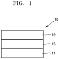
- FIG. 1 is a schematic view of an organic light-emitting device 10 according to an embodiment.
- the organic light-emitting device 10 includes a first electrode 11, an organic layer 15, and a second electrode 19, which are sequentially stacked.
- a substrate may be additionally disposed under the first electrode 11 or above the second electrode 19.
- the substrate any substrate that is used in general organic light-emitting devices may be used, and the substrate may be a glass substrate or a transparent plastic substrate, each having excellent mechanical strength, thermal stability, transparency, surface smoothness, ease of handling, and water resistance.
- the first electrode 11 may be formed by depositing or sputtering a material for forming the first electrode 11 on the substrate.
- the first electrode 11 may be an anode.
- the material for forming the first electrode 11 may be selected from materials with a high work function to facilitate hole injection.
- the first electrode 11 may be a reflective electrode, a semi-transmissive electrode, or a transmissive electrode.
- the material for forming the first electrode may be, for example, indium tin oxide (ITO), indium zinc oxide (IZO), tin oxide (SnO 2 ), and zinc oxide (ZnO).
- magnesium (Mg), aluminum (Al), aluminum-lithium (Al-Li), calcium (Ca), magnesium-indium (Mg-In), or magnesium-silver (Mg-Ag) may be used as the material for forming the first electrode.
- the first electrode 11 may have a single-layered structure or a multi-layered structure including two or more layers.
- the first electrode 11 may have a three-layered structure of ITO/Ag/ITO, but the structure of the first electrode 110 is not limited thereto.
- the organic layer 15 is disposed on the first electrode 11.
- the organic layer 15 may include a hole transport region, an emission layer, and an electron transport region.
- the hole transport region may be disposed between the first electrode 11 and the emission layer.
- the hole transport region may include at least one selected from a hole injection layer, a hole transport layer, an electron blocking layer, and a buffer layer.
- the hole transport region may include only either a hole injection layer or a hole transport layer.
- the hole transport region may have a hole injection layer/hole transport layer structure or a hole injection layer/hole transport layer/electron blocking layer structure, which are sequentially stacked in this stated order from the first electrode 11.
- a hole injection layer may be formed on the first electrode 11 by using one or more suitable methods selected from vacuum deposition, spin coating, casting, or Langmuir-Blodgett (LB) deposition.
- suitable methods selected from vacuum deposition, spin coating, casting, or Langmuir-Blodgett (LB) deposition.
- the deposition conditions may vary according to a compound that is used to form the hole injection layer, and the structure and thermal characteristics of the hole injection layer.
- the deposition conditions may include a deposition temperature of about 100°C to about 500°C, a vacuum pressure of about 10 -8 torr to about 10 -3 torr, and a deposition rate of about 0.01 ⁇ /sec to about 100 ⁇ /sec.
- the deposition conditions are not limited thereto.
- coating conditions may vary according to the material used to form the hole injection layer, and the structure and thermal properties of the hole injection layer.
- a coating speed may be from about 2,000 revolutions per minute (rpm) to about 5,000 rpm
- a temperature at which a heat treatment is performed to remove a solvent after coating may be from about 80°C to about 200°C.
- the coating conditions are not limited thereto.
- Conditions for forming a hole transport layer and an electron blocking layer may be understood by referring to conditions for forming the hole injection layer.
- the hole transport region may include at least one selected from m-MTDATA, TDATA, 2-TNATA, NPB, ⁇ -NPB, TPD, spiro-TPD, spiro-NPB, methylated-NPB, TAPC, HMTPD, 4,4',4"-tris(N-carbazolyl)triphenylamine (TCTA), polyaniline/dodecylbenzene sulfonic acid (PANI/DBSA), poly(3,4-ethylenedioxythiophene)/poly(4-styrenesulfonate) (PEDOT/PSS), polyaniline/camphor sulfonic acid (PANI/CSA), polyaniline/poly(4-styrene sulfonate) (PANI/PSS), a compound represented by Formula 201 below, and a compound represented by Formula 202 below: Ar 101 and Ar 102 in Formula 201 may each independently be selected from:
- the compound represented by Formula 201 may be represented by Formula 201A, but embodiments of the present disclosure are not limited thereto:
- R 101 , R111 , R 112 , and R 109 in Formula 201A may be understood by referring to the description provided herein.
- the compound represented by Formula 201 and the compound represented by Formula 202 may include compounds HT1 to HT20 illustrated below, but are not limited thereto.
- a thickness of the hole transport region may be in a range of about 100 ⁇ to about 10,000 ⁇ , for example, about 100 ⁇ to about 3,000 ⁇ .
- the thickness of the hole injection layer may be in a range of about 100 ⁇ to about 10,000 ⁇ , for example, about 100 ⁇ to about 2,000 ⁇
- the thickness of the hole transport layer may be in a range of about 50 ⁇ to about 2,000 ⁇ , for example, about 100 ⁇ to about 1,500 ⁇ . While not wishing to be bound by theory, it is understood that when the thicknesses of the hole transport region, the hole injection layer and the hole transport layer are within these ranges, satisfactory hole transporting characteristics may be obtained without a substantial increase in driving voltage.
- the hole transport region may further include, in addition to these materials, a charge-generation material for the improvement of conductive properties.
- the charge-generation material may be homogeneously or non-homogeneously dispersed in the hole transport region.
- the charge-generation material may be, for example, a p-dopant.
- the p-dopant may be one selected from a quinone derivative, a metal oxide, and a cyano group-containing compound, but embodiments of the present disclosure are not limited thereto.
- Non-limiting examples of the p-dopant are a quinone derivative, such as tetracyanoquinonedimethane (TCNQ) or 2,3,5,6-tetrafluoro-tetracyano-1,4-benzoquinonedimethane (F4-TCNQ); a metal oxide, such as a tungsten oxide or a molybdenium oxide; and a cyano group-containing compound, such as Compound HT-D1 or Compound HT-D2 below, but are not limited thereto.
- a quinone derivative such as tetracyanoquinonedimethane (TCNQ) or 2,3,5,6-tetrafluoro-tetracyano-1,4-benzoquinonedimethane (F4-TCNQ)
- a metal oxide such as a tungsten oxide or a molybdenium oxide
- a cyano group-containing compound such as Compound HT-D1 or Compound
- the hole transport region may include a buffer layer.
- the buffer layer may compensate for an optical resonance distance according to a wavelength of light emitted from the emission layer, and thus, efficiency of a formed organic light-emitting device may be improved.
- the hole transport region may further include an electron blocking layer.
- the electron blocking layer may include, for example, mCP, but a material therefor is not limited thereto.
- the host included in the emission layer may be used, but the embodiments are not limited thereto.
- an emission layer may be formed on the hole transport region by vacuum deposition, spin coating, casting, LB deposition, or the like.
- the deposition or coating conditions may be similar to those applied in forming the hole injection layer although the deposition or coating conditions may vary according to a compound that is used to form the emission layer.
- the emission layer may be patterned into a red emission layer, a green emission layer, and a blue emission layer.
- the emission layer may emit white light.
- the emission layer may include the TADF emitter and the host described above.
- the emission layer may consist of the TADF emitter and the host described above.
- a thickness of the emission layer may be in a range of about 100 ⁇ to about 1,000 ⁇ , for example, about 200 ⁇ to about 600 ⁇ . While not wishing to be bound by theory, it is understood that when the thickness of the emission layer is within this range, excellent light-emission characteristics may be obtained without a substantial increase in driving voltage.
- an electron transport region may be disposed on the emission layer.
- the electron transport region may include at least one selected from a hole blocking layer, an electron transport layer, and an electron injection layer.
- the electron transport region may have a hole blocking layer/electron transport layer/electron injection layer structure or an electron transport layer/electron injection layer structure, but the structure of the electron transport region is not limited thereto.
- the electron transport layer may have a single-layered structure or a multi-layered structure including two or more different materials.
- Conditions for forming the hole blocking layer, the electron transport layer, and the electron injection layer which constitute the electron transport region may be understood by referring to the conditions for forming the hole injection layer.
- the hole blocking layer may include, for example, at least one of BCP and Bphen, but may also include other materials.
- the hole blocking material a compound that is identical to the host included in the emission layer may be used, but the embodiments are not limited thereto.
- a thickness of the hole blocking layer may be in a range of about 20 ⁇ to about 1,000 ⁇ , for example, about 30 ⁇ to about 300 ⁇ . While not wishing to be bound by theory, it is understood that when the thickness of the hole blocking layer is within these ranges, the hole blocking layer may have improved hole blocking ability without a substantial increase in driving voltage.
- the electron transport layer may include at least one selected from BCP, Bphen, Alq 3 , BAlq, TAZ, and NTAZ.
- the electron transport layer may include at least one of ET1 to ET25, but are not limited thereto:
- a thickness of the electron transport layer may be in a range of about 100 ⁇ to about 1,000 ⁇ , for example, about 150 ⁇ to about 500 ⁇ . While not wishing to be bound by theory, it is understood that when the thickness of the electron transport layer is within the range described above, the electron transport layer may have satisfactory electron transport characteristics without a substantial increase in driving voltage.
- the electron transport layer may further include, in addition to the materials described above, a metal-containing material.
- the metal-containing material may include a Li complex.
- the Li complex may include, for example, Compound ET-D1 (lithium 8-hydroxyquinolate, LiQ) or ET-D2.
- the electron transport region may include an electron injection layer that promotes flow of electrons from the second electrode 19 thereinto.
- the electron injection layer may include at least one selected from LiF, NaCl, CsF, Li 2 O, and BaO.
- a thickness of the electron injection layer may be in a range of about 1 ⁇ to about 100 ⁇ , for example, about 3 ⁇ to about 90 ⁇ . While not wishing to be bound by theory, it is understood that when the thickness of the electron injection layer is within the range described above, the electron injection layer may have satisfactory electron injection characteristics without a substantial increase in driving voltage.
- the second electrode 19 is disposed on the organic layer 15.
- the second electrode 19 may be a cathode.
- a material for forming the second electrode 19 may be selected from metal, an alloy, an electrically conductive compound, and a combination thereof, which have a relatively low work function.
- lithium (Li), magnesium (Mg), aluminum (Al), aluminum-lithium (Al-Li), calcium (Ca), magnesium-indium (Mg-In), or magnesium-silver (Mg-Ag) may be used as a material for forming the second electrode 19.
- a transmissive electrode formed using ITO or IZO may be used as the second electrode 19.
- C 1 -C 60 alkyl group refers to a linear or branched saturated aliphatic hydrocarbon monovalent group having 1 to 60 carbon atoms, and non-limiting examples thereof include a methyl group, an ethyl group, a propyl group, an iso-butyl group, a sec-butyl group, a tert-butyl group, a pentyl group, an iso-amyl group, and a hexyl group.
- C 1 -C 60 alkylene group refers to a divalent group having the same structure as the C 1 -C 60 alkyl group.
- C 1 -C 60 alkoxy group refers to a monovalent group represented by -OA 101 (wherein A 101 is the C 1 -C 60 alkyl group), and non-limiting examples thereof include a methoxy group, an ethoxy group, and an iso-propyloxy group.
- C 2 -C 60 alkenyl group refers to a hydrocarbon group formed by including at least one carbon-carbon double bond in the middle or at the terminus of the C 2 -C 60 alkyl group, and examples thereof include an ethenyl group, a propenyl group, and a butenyl group.
- C 2 -C 60 alkenylene group refers to a divalent group having the same structure as the C 2 -C 60 alkenyl group.
- C 2 -C 60 alkynyl group refers to a hydrocarbon group formed by including at least one carbon-carbon triple bond in the middle or at the terminus of the C 2 -C 60 alkyl group, and examples thereof include an ethynyl group, and a propynyl group.
- C 2 -C 60 alkynylene group refers to a divalent group having the same structure as the C 2 -C 60 alkynyl group.
- C 3 -C 10 cycloalkyl group refers to a monovalent saturated hydrocarbon monocyclic group having 3 to 10 carbon atoms, and non-limiting examples thereof include a cyclopropyl group, a cyclobutyl group, a cyclopentyl group, a cyclohexyl group, and a cycloheptyl group.
- C 3 -C 10 cycloalkylene group refers to a divalent group having the same structure as the C 3 -C 10 cycloalkyl group.
- C 1 -C 10 heterocycloalkyl group refers to a monovalent saturated monocyclic group having at least one heteroatom selected from N, O, P, Si and S as a ring-forming atom and 1 to 10 carbon atoms, and non-limiting examples thereof include a tetrahydrofuranyl group, and a tetrahydrothiophenyl group.
- C 1 -C 10 heterocycloalkylene group refers to a divalent group having the same structure as the C 1 -C 10 heterocycloalkyl group.
- C 3 -C 10 cycloalkenyl group refers to a monovalent monocyclic group that has 3 to 10 carbon atoms, at least one carbon-carbon double bond in the ring thereof, and no aromaticity, and non-limiting examples thereof include a cyclopentenyl group, a cyclohexenyl group, and a cycloheptenyl group.
- C 3 -C 10 cycloalkenylene group refers to a divalent group having the same structure as the C 3 -C 10 cycloalkenyl group.
- C 1 -C 10 heterocycloalkenyl group refers to a monovalent monocyclic group that has at least one heteroatom selected from N, O, P, Si, and S as a ring-forming atom, 1 to 10 carbon atoms, and at least one carbon-carbon double bond in its ring.
- Examples of the C 1 -C 10 heterocycloalkenyl group are a 2,3-dihydrofuranyl group, and a 2,3-dihydrothiophenyl group.
- C 1 -C 10 heterocycloalkenylene group refers to a divalent group having the same structure as the C 1 -C 10 heterocycloalkenyl group.
- C 6 -C 60 aryl group refers to a monovalent group having a carbocyclic aromatic system having 6 to 60 carbon atoms
- C 6 -C 60 arylene group refers to a divalent group having a carbocyclic aromatic system having 6 to 60 carbon atoms.
- Non-limiting examples of the C 6 -C 60 aryl group include a phenyl group, a naphthyl group, an anthracenyl group, a phenanthrenyl group, a pyrenyl group, and a chrysenyl group.
- the C 6 -C 60 aryl group and the C 6 -C 60 arylene group each include two or more rings, the rings may be fused to each other.
- C 1 -C 60 heteroaryl group refers to a monovalent group having a heterocyclic aromatic system that has at least one heteroatom selected from N, O, P, and S as a ring-forming atom, and 1 to 60 carbon atoms.
- C 1 -C 60 heteroarylene group refers to a divalent group having a heterocyclic aromatic system that has at least one heteroatom selected from N, O, P, and S as a ring-forming atom, and 1 to 60 carbon atoms.
- Non-limiting examples of the C 1 -C 60 heteroaryl group include a pyridinyl group, a pyrimidinyl group, a pyrazinyl group, a pyridazinyl group, a triazinyl group, a quinolinyl group, and an isoquinolinyl group.
- the C 1 -C 60 heteroaryl group and the C 1 -C 60 heteroarylene group each include two or more rings, the rings may be fused to each other.
- C 6 -C 60 aryloxy group indicates -OA 102 (wherein A 102 is the C 6 -C 60 aryl group), a C 6 -C 60 arylthio group as used herein indicates -SA 103 (wherein A 103 is the C 6 -C 60 aryl group), and the term "C 7 -C 60 arylalkyl group” as used herein indicates -A 104 A 105 (wherein A 104 is the C 6 -C 59 aryl group and A 105 is the C 1 -C 53 alkyl group).
- C 1 -C 60 heteroaryloxy group refers to -OA 106 (wherein A 106 is the C 2 -C 60 heteroaryl group), and the term “C 1 -C 60 heteroarylthio group” as used herein indicates -SA 107 (wherein A 107 is the C 2 -C 60 heteroaryl group).
- C 2 -C 60 heteroarylalkyl group refers to -A 108 A 109 (A 109 is a C 2 -C 59 heteroaryl group, and A 108 is a C 1 -C 58 alkylene group).
- monovalent non-aromatic condensed polycyclic group refers to a monovalent group (for example, having 8 to 60 carbon atoms) having two or more rings condensed to each other, only carbon atoms as ring-forming atoms, and no aromaticity in its entire molecular structure.
- monovalent non-aromatic condensed polycyclic group include a fluorenyl group.
- divalent non-aromatic condensed polycyclic group refers to a divalent group having the same structure as the monovalent non-aromatic condensed polycyclic group.
- the term "monovalent non-aromatic condensed heteropolycyclic group” as used herein refers to a monovalent group (for example, having 2 to 60 carbon atoms) having two or more rings condensed to each other, a heteroatom selected from N, O, P, Si, and S, other than carbon atoms, as a ring-forming atom, and no aromaticity in its entire molecular structure.
- Non-limiting examples of the monovalent non-aromatic condensed heteropolycyclic group include a carbazolyl group.
- divalent non-aromatic condensed heteropolycyclic group refers to a divalent group having the same structure as the monovalent non-aromatic condensed heteropolycyclic group.
- C 5 -C 30 carbocyclic group refers to a saturated or unsaturated cyclic group having, as a ring-forming atom, 5 to 30 carbon atoms only.
- the C 5 -C 30 carbocyclic group may be a monocyclic group or a polycyclic group.
- C 1 -C 30 heterocyclic group refers to a saturated or unsaturated cyclic group having, as a ring-forming atom, at least one heteroatom selected from N, O, Si, P, and S other than 1 to 30 carbon atoms.
- the C 1 -C 30 heterocyclic group may be a monocyclic group or a polycyclic group.
- room temperature refers to about 25°C.
- organic light-emitting device According to embodiments are described in detail with reference to. However, the organic light-emitting device is not limited thereto.
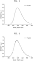
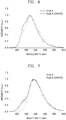
- photoluminescence (PL) spectra of the films 1, 2, 3, 3 (DPEPO), 4, A, A (DPEPO), B, and B (DPEPO) were evaluated by using an ISC PC1 spectrofluorometer equipped with a xenon lamp. Evaluation results are shown in FIG. 2 (PL spectrum of the film 1), FIG. 3 (PL spectrum of the film 2), FIG. 4 (PL spectra of the film 3 and the film 3 (DPEPO)), FIG. 5 (PL spectrum of the film 4), FIG. 6 (PL spectra of the film A and the film A (DPEPO)), and FIG.
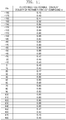
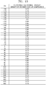
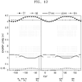
- the attachment-detachment overlap densities of the each rotamers (10x°) of Compounds 1 to 4 and Compounds A and B are shown in Table 3 with reference to FIGS. 8 to 13 .
- Table 3 Compound No. Range including 10x at which the attachment-detachment overlap density of the corresponding rotamer(10x°) is 0.65 or more Whether Compound satisfies Condition 2-1 1 1 -180 ⁇ -170 X -130 ⁇ 0 40 ⁇ 180 2 -130 ⁇ -50 X 50 ⁇ 130 3 None ⁇ 4 -140 ⁇ -40 X 40 ⁇ 140 A -130 ⁇ -20 X 60 ⁇ 160 B -180 ⁇ 180 X 1 : a condition that attachment-detachment overlap densities of all rotamer(10x°) are less than 0.65
- TCSPC Time-Correlated Single Photon Counting
- T decay (Ex) of the films 1, 2, 3, 4, A, and B was obtained by fitting two or more exponential decay functions to a result obtained from the TRPL curve.
- the function used in fitting was equal to Equation 1, and the greatest value of T decay obtained from the exponential decay functions used in fitting was taken as T decay (Ex).
- the other T decay values may be used to determine a lifetime of a general fluorescence decay lifetime.
- a baseline or background signal curve was obtained by repeating the same measurement once more in a dark state (a state in which a pumping signal incident on the film was blocked) for the same time as the measurement time for obtaining the TRPL curve, and the obtained a baseline or background signal curve was used as a baseline in fitting.
- the films 1 to 4 respectively including Compounds 1 to 4 as an emitter have excellent delayed fluorescence characteristics, as compared with those of the films A and B respectively including Compounds A and B as an emitter.
- Photoluminescent quantum yields in the films 1, 2, 4, A, and B manufactured according to Evaluation Example 1 were evaluated by using a Hamamatsu Photonics absolute PL quantum yield measurement system equipped with a xenon light source, a monochromator, a photonic multichannel analyzer, and an integrating sphere and using PLQY measurement software (Hamamatsu Photonics, Ltd., Shizuoka, Japan). Evaluation results are shown in Table 6. Table 6 Film No. PLQY in film Film 1 0.735 Film 2 0.782 Film 4 0.531 Film A 0.425 Film B 0.147
- the films 1, 2, and 4 respectively including Compounds 1, 2, and 4 as an emitter have excellent photoluminescent quantum yields, as compared with the films A and B respectively including Compounds A and B as an emitter.
- UV ultraviolet
- Compound HT3 and HT-D2 (a concentration of HT-D2 was 3 percent by weight, wt%) were co-deposited on the anode to form a hole injection layer having a thickness of 100 ⁇
- Compound HT3 was deposited on the hole injection layer to form a hole transport layer having a thickness of 1,500 ⁇
- mCP was deposited on the hole transport layer to form an electron blocking layer having a thickness of 100 ⁇ , thereby forming a hole transport region having a thickness of 1,700 ⁇ .
- Compound H19 (host) and Compound 1 (dopant) were co-deposited on the hole transport region at a volume ratio of 9:1 to form an emission layer having a thickness of 400 ⁇ .
- Compound H19 was vacuum-deposited on the emission layer to form a hole blocking layer having a thickness of 100 ⁇
- Compound ET17 and LiQ were co-deposited on the hole blocking layer at a weight ratio of 5:5 to form an electron transport layer having a thickness of 360 ⁇
- LiQ was deposited on the electron transport layer to form an electron injection layer having a thickness of 5 ⁇
- Al was vacuum-deposited on the electron injection layer to form a cathode having a thickness of 120 ⁇ , thereby completing the manufacture of an organic light-emitting device.
- Organic light-emitting devices were manufactured in the same manner as in Example 1, except that Compounds shown in Table 7 were each used as a dopant in forming an emission layer.
- an organic light-emitting device including a TADF emitter satisfying Condition 1-1 or Condition 1-2 may have excellent delayed fluorescence characteristics, regardless of a type of a host used together in an emission layer, the organic light-emitting device including the TADF emitter may have excellent characteristics in terms of quantum efficiency and roll-off ratio.
Landscapes
- Physics & Mathematics (AREA)
- Chemical & Material Sciences (AREA)
- Engineering & Computer Science (AREA)
- Materials Engineering (AREA)
- Spectroscopy & Molecular Physics (AREA)
- Optics & Photonics (AREA)
- Organic Chemistry (AREA)
- Manufacturing & Machinery (AREA)
- Electroluminescent Light Sources (AREA)
Abstract
Description
- One or more embodiments relate to an organic light-emitting device.
- Organic light-emitting devices (OLEDs) are self-emission devices that produce full-color images, and also have wide viewing angles, high contrast ratios, short response times, as well as excellent characteristics in terms of brightness, driving voltage, and response speed.
- An example of such organic light-emitting devices may include an anode, a cathode, and an organic layer that is disposed between the anode and the cathode, wherein the organic layer includes an emission layer. A hole transport region may be disposed between the anode and the emission layer, and an electron transport region may be disposed between the emission layer and the cathode. Holes provided from the anode may move toward the emission layer through the hole transport region, and electrons provided from the cathode may move toward the emission layer through the electron transport region. Carriers, such as holes and electrons, recombine in an emission layer to produce excitons. These excitons transit from an excited state to a ground state, thereby generating light.
- Various types of organic light emitting devices are known. However, there still remains a need in OLEDs having low driving voltage, high efficiency, high brightness, and long lifespan.
- One or more embodiments include an organic light-emitting device that includes a host and a dopant satisfying a certain condition and has excellent characteristics in terms of external quantum efficiency and roll-off ratio.
- Additional aspects will be set forth in part in the description which follows and, in part, will be apparent from the description, or may be learned by practice of the presented embodiments.
- According to one or more embodiments, an organic light-emitting device includes:
- a first electrode;
- a second electrode facing the first electrode; and
- an organic layer that is disposed between the first electrode and the second electrode, wherein the organic layer includes an emission layer,
- wherein the emission layer includes a thermally activated delayed fluorescence (TADF) emitter and a host and the TADF emitter is different from the host, and
- the TADF emitter satisfies Condition 1-1 or Condition 1-2:
- Condition 1-1
a condition that n1 is one, and - Condition 1-2
a condition that, when n1 is two or more, (I1 / I2) x 100(%) is less than 110%. In Condition 1-1 and Condition 1-2,
- Condition 1-1
- I1 (arbitrary units) is emission intensity at the shortest peak emission wavelength in a
photoluminescence spectrum 1,- 1) when n2 is one, I2 (arbitrary units) is emission intensity at the same peak emission wavelength as the shortest emission wavelength of the
photoluminescence spectrum 1 in thephotoluminescence spectrum 2, and 2) when n2 is two or more, I2 (arbitrary units) is emission intensity at the shortest peak emission wavelength in aphotoluminescence spectrum 2,
- 1) when n2 is one, I2 (arbitrary units) is emission intensity at the same peak emission wavelength as the shortest emission wavelength of the
- the
photoluminescence spectrum 1 is a photoluminescence spectrum of afilm 1 that is doped with 15 percent by volume of the TADF emitter in a matrix with the host included in the emission layer and has a thickness of 50 nanometers, and - the
photoluminescence spectrum 2 is a photoluminescence spectrum of afilm 2 that is doped with 15 percent by volume of the TADF emitter in a matrix with DPEPO and has a thickness of 50 nanometers:
photoluminescence spectrum 1, and n2 is the number of distinguishable emission peaks in thephotoluminescence spectrum 2. - These and/or other aspects will become apparent and more readily appreciated from the following description of the embodiments, taken in conjunction with the accompanying drawings in which:
-
FIG. 1 is a schematic view of an organic light-emitting device according to an embodiment; -
FIGS. 2 to 7 are graphs of intensity (arbitrary units, a.u.) versus wavelength (nanometers, nm), which illustrate photoluminescence spectra offilm -
FIGS. 8 to 13 are tables showing attachment-detachment overlap densities of rotamers (10x°) ofCompounds -
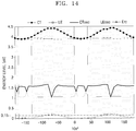
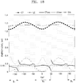
FIG. 14 is a graph showing rotational conformational energy (electron volts, eV), CTosc (electron volts, eV), LEosc (electron volts, eV), a charge transfer state (CT) energy level (electron volts, eV), and a locally excited state (LE) energy level (electron volts, eV) with respect to each rotamer (10x°) ofCompound 1; -
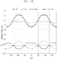
FIG. 15 is a graph showing rotational conformational energy (electron volts, eV), CTosc (electron volts, eV), LEosc (electron volts, eV), a CT energy level (electron volts, eV), and an LE energy level (electron volts, eV) with respect to each rotamer (10x°) ofCompound 2; -
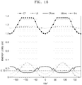
FIG. 16 is a graph showing rotational conformational energy (electron volts, eV), CTosc (electron volts, eV), LEosc (electron volts, eV), a CT energy level (electron volts, eV), and an LE energy level (electron volts, eV) with respect to each rotamer (10x°) ofCompound 4; -
FIG. 17 is a graph showing rotational conformational energy (electron volts, eV), CTosc (electron volts, eV), LEosc (electron volts, eV), a CT energy level (electron volts, eV), and an LE energy level (electron volts, eV) with respect to each rotamer (10x°) of Compound A; and -
FIG. 18 is a graph showing rotational conformational energy (electron volts, eV), CTosc (electron volts, eV), LEosc (electron volts, eV), a CT energy level (electron volts, eV), and an LE energy level (electron volts, eV) with respect to each rotamer (10x°) of Compound B. - Reference will now be made in detail to embodiments, examples of which are illustrated in the accompanying drawings, wherein like reference numerals refer to like elements throughout. In this regard, the present embodiments may have different forms and should not be construed as being limited to the descriptions set forth herein. Accordingly, the embodiments are merely described below, by referring to the figures, to explain aspects of the present description. As used herein, the term "and/or" includes any and all combinations of one or more of the associated listed items. Expressions such as "at least one of," when preceding a list of elements, modify the entire list of elements and do not modify the individual elements of the list.
- It will be understood that when an element is referred to as being "on" another element, it can be directly in contact with the other element or intervening elements may be present therebetween. In contrast, when an element is referred to as being "directly on" another element, there are no intervening elements present.
- It will be understood that, although the terms first, second, third etc. may be used herein to describe various elements, components, regions, layers, and/or sections, these elements, components, regions, layers, and/or sections should not be limited by these terms. These terms are only used to distinguish one element, component, region, layer, or section from another element, component, region, layer, or section. Thus, a first element, component, region, layer, or section discussed below could be termed a second element, component, region, layer, or section without departing from the teachings of the present embodiments.
- The terminology used herein is for the purpose of describing particular embodiments only and is not intended to be limiting. As used herein, the singular forms "a," "an," and "the" are intended to include the plural forms as well, unless the context clearly indicates otherwise.
- The term "or" means "and/or." It will be further understood that the terms "comprises" and/or "comprising," or "includes" and/or "including" when used in this specification, specify the presence of stated features, regions, integers, steps, operations, elements, and/or components, but do not preclude the presence or addition of one or more other features, regions, integers, steps, operations, elements, components, and/or groups thereof.
- Unless otherwise defined, all terms (including technical and scientific terms) used herein have the same meaning as commonly understood by one of ordinary skill in the art to which this general inventive concept belongs. It will be further understood that terms, such as those defined in commonly used dictionaries, should be interpreted as having a meaning that is consistent with their meaning in the context of the relevant art and the present disclosure, and will not be interpreted in an idealized or overly formal sense unless expressly so defined herein.
- Exemplary embodiments are described herein with reference to cross section illustrations that are schematic illustrations of idealized embodiments. As such, variations from the shapes of the illustrations as a result, for example, of manufacturing techniques and/or tolerances, are to be expected. Thus, embodiments described herein should not be construed as limited to the particular shapes of regions as illustrated herein but are to include deviations in shapes that result, for example, from manufacturing. For example, a region illustrated or described as flat may, typically, have rough and/or nonlinear features. Moreover, sharp angles that are illustrated may be rounded. Thus, the regions illustrated in the figures are schematic in nature and their shapes are not intended to illustrate the precise shape of a region and are not intended to limit the scope of the present claims.
- "About" or "approximately" as used herein is inclusive of the stated value and means within an acceptable range of deviation for the particular value as determined by one of ordinary skill in the art, considering the measurement in question and the error associated with measurement of the particular quantity (i.e., the limitations of the measurement system). For example, "about" can mean within one or more standard deviations, or within ± 30%, 20%, 10%, 5% of the stated value.
- In an embodiment, an organic light-emitting device is provided. The organic light-emitting device, according to an embodiment, may include:
- a first electrode;
- a second electrode facing the first electrode; and
- an organic layer that is disposed between the first electrode and the second electrode, wherein the organic layer includes an emission layer,
- wherein the emission layer includes a thermally activated delayed fluorescence (TADF) emitter and a host and the TADF emitter is different from the host, provided that the TADF emitter satisfies Condition 1-1 or Condition 1-2:
- Condition 1-1
a condition that n1 is one, and - Condition 1-2
a condition that, when n1 is two or more, (I1 / I2) x 100(%) is less than 110%. In Condition 1-1 and Condition 1-2,
- Condition 1-1
- I1 (a.u.) is emission intensity at the shortest peak emission wavelength in a
photoluminescence spectrum 1, wherein "a.u." denotes "arbitrary units",- 1) when n2 is one, I2 (a.u.) is emission intensity at the same emission wavelength as the shortest peak emission wavelength of the
photoluminescence spectrum 1 in thephotoluminescence spectrum 2, and 2) when n2 is two or more, I2 (a.u.) is emission intensity at the shortest peak emission wavelength in aphotoluminescence spectrum 2,
- 1) when n2 is one, I2 (a.u.) is emission intensity at the same emission wavelength as the shortest peak emission wavelength of the
- the
photoluminescence spectrum 1 is a photoluminescence spectrum of afilm 1 that is doped with 15 percent by volume (vol%) of the TADF emitter in a matrix with the host included in the emission layer and has a thickness of 50 nanometers (nm), and - the
photoluminescence spectrum 2 is a photoluminescence spectrum of afilm 2 that is doped with 15 vol% of the TADF emitter in a matrix with DPEPO and has a thickness of 50 nm:
photoluminescence spectrum 1, and n2 is the number of distinguishable emission peaks in thephotoluminescence spectrum 2. - For example, the I1 and the I2 may have same unit.
- For example, the host may not include DPEPO.
- When the TADF emitter satisfies Condition 1-1 or Condition 1-2, the TADF emitter may have excellent delayed fluorescence characteristics without severe dual fluorescence.
- In an embodiment, the TADF emitter may be a compound represented by Formula 1:
Formula 1 R1-(D2)d1-D1-(L1)a1-A1.
InFormula 1, - L1 may be selected from:
- a single bond, a cyclopentane group, a cyclohexane group, a cycloheptane group, a cyclooctane group, a cyclopenpentene group, a cyclohexene group, a cycloheptene group, a benzene group, a naphthalene group, a fluorene group, a phenanthrene group, an anthracene group, a fluoranthene group, a triphenylene group, a pyrene group, a chrysene group, a pyrrole group, a thiophene group, a furan group, an imidazole group, a pyrazole group, a thiazole group, an isothiazole group, an oxazole group, an isoxazole group, a pyridine group, a pyrazine group, a pyrimidine group, a pyradizine group, an iso-indole group, an indole group, an indazole group, a purine group, a quinoline group, an isoquinoline group, a benzoquinoline group, a quinoxaline group, a quinazoline group, a cinnoline group, a phenanthroline group, a benzimidazole group, a benzofuran group, a benzothiophene group, a benzoxazole group, an isobenzoxazole group, a triazole group, a tetrazole group, an oxadiazole group, a triazine group, a dibenzofuran group, a dibenzothiophene group, a benzocarbazole group, a dibenzocarbazole group, an imidazopyridine group, an imidazopyrimidine group, an azaindole group, an azaindene group, an azabenzofuran group, an azabenzothiophene group, an azacarbazole group, an azafluorene group, an azadibenzofuran group, and an azadibenzothiophene group; and
- a cyclopentane group, a cyclohexane group, a cycloheptane group, a cyclooctane group, a cyclopenpentene group, a cyclohexene group, a cycloheptene group, a benzene group, a naphthalene group, a fluorene group, a phenanthrene group, an anthracene group, a fluoranthene group, a triphenylene group, a pyrene group, a chrysene group, a pyrrole group, a thiophene group, a furan group, an imidazole group, a pyrazole group, a thiazole group, an isothiazole group, an oxazole group, an isoxazole group, a pyridine group, a pyrazine group, a pyrimidine group, a pyradizine group, an iso-indole group, an indole group, an indazole group, a purine group, a quinoline group, an isoquinoline group, a benzoquinoline group, a quinoxaline group, a quinazoline group, a cinnoline group, a phenanthroline group, a benzimidazole group, a benzofuran group, a benzothiophene group, a benzoxazole group, an isobenzoxazole group, a triazole group, a tetrazole group, an oxadiazole group, a triazine group, a dibenzofuran group, a dibenzothiophene group, a benzocarbazole group, a dibenzocarbazole group, an imidazopyridine group, an imidazopyrimidine group, an azaindole group, an azaindene group, an azabenzofuran group, an azabenzothiophene group, an azacarbazole group, an azafluorene group, an azadibenzofuran group, and an azadibenzothiophene group, each substituted with at least one selected from deuterium, -F, -Cl, -Br, -I, -CD3, -CD2H, -CDH2, -CF3, -CF2H,-CFH2, a hydroxyl group, a cyano group, a nitro group, an amino group, an amidino group, a hydrazine group, a hydrazone group, a carboxylic acid group or a salt thereof, a sulfonic acid group or a salt thereof, a phosphoric acid group or a salt thereof, a C1-C20 alkyl group, a C1-C20 alkoxy group, a phenyl group, a (C1-C20 alkyl)phenyl group, a di(C1-C20 alkyl)phenyl group, a tri(C1-C20 alkyl)phenyl group, a (C6-C20 aryl)phenyl group, a di(C6-C20 aryl)phenyl group, a tri(C6-C20 aryl)phenyl group, a (C3-C20 heteroaryl)phenyl group, a di(C3-C20 heteroaryl)phenyl group, a pyridinyl group, a (C1-C20 alkyl)pyridinyl group, a di(C1-C20 alkyl)pyridinyl group, a (C6-C20 aryl)pyridinyl group, a di(C6-C20 aryl)pyridinyl group, a (C3-C20 heteroaryl)pyridinyl group, a di(C3-C20 heteroaryl)pyridinyl group, a pyrimidinyl group, a (C1-C20 alkyl)pyrimidinyl group, a di(C1-C20 alkyl)pyrimidinyl group, a (C6-C20 aryl)pyrimidinyl group, a di(C6-C20 aryl)pyrimidinyl group, a (C3-C20 heteroaryl)pyrimidinyl group, a di(C3-C20 heteroaryl)pyrimidinyl group, a triazinyl group, a (C1-C20 alkyl)triazinyl group, a di(C1-C20 alkyl)triazinyl group, a (C6-C20 aryl)triazinyl group, a di(C6-C20 aryl)triazinyl group, a (C3-C20 heteroaryl)triazinyl group, and a di(C3-C20 heteroaryl)triazinyl group,
- a1 may be an integer from 1 to 5,
- D1 and D2 may each be an electron donor group,
- d1 may be an integer from 0 to 5,
- A1 may be an electron acceptor group, and
- R1 may be selected from:
- hydrogen, deuterium, a C1-C60 alkyl group, a C2-C60 alkenyl group, a C2-C60 alkynyl group, a C1-C60 alkoxy group, a C5-C60 carbocyclic group, and a π electron-depleted nitrogen-free C2-C60 heterocyclic group; and
- a C1-C60 alkyl group, a C2-C60 alkenyl group, a C2-C60 alkynyl group, a C1-C60 alkoxy group, a C5-C60 carbocyclic group, and a π electron-depleted nitrogen-free C2-C60 heterocyclic group, each substituted with at least one selected from deuterium, a C1-C60 alkyl group, a C2-C60 alkenyl group, a C2-C60 alkynyl group, a C1-C60 alkoxy group, a C5-C60 carbocyclic group, a (C1-C10 alkyl)C5-C60 carbocyclic group, a di(C1-C10 alkyl)C5-C60 carbocyclic group, a (phenyl)C5-C60 carbocyclic group, a di(phenyl)C5-C60 carbocyclic group, a (biphenyl)C5-C60 carbocyclic group, a di(biphenyl)C5-C60 carbocyclic group, a π electron-depleted nitrogen-free C2-C60 heterocyclic group, a (C1-C10 alkyl) π electron-depleted nitrogen-free C2-C60 heterocyclic group, a di(C1-C10 alkyl) π electron-depleted nitrogen-free C2-C60 heterocyclic group, a (phenyl) π electron-depleted nitrogen-free C2-C60 heterocyclic group, a di(phenyl) π electron-depleted nitrogen-free C2-C60 heterocyclic group, a (biphenyl) π electron-depleted nitrogen-free C2-C60 heterocyclic group, and a di(biphenyl) π electron-depleted nitrogen-free C2-C60 heterocyclic group,
- provided that,
- i) d1 is an integer from 1 to 5; or
- ii) when d1 is zero, A1 is selected from groups represented by Formulae 3-6(1), 3-10(8), and 3-12(24):

- X41 may be N(R41), C(R42)(R43), O, or S,
- R31, R32, R34 to R37 and R41 to R43 may each independently be selected from hydrogen, deuterium, -F, -Cl, -Br, -I, -CD3, -CD2H, -CDH2, -CF3, -CF2H, - CFH2, a hydroxyl group, a cyano group, a nitro group, an amino group, an amidino group, a hydrazine group, a hydrazone group, a carboxylic acid group or a salt thereof, a sulfonic acid group or a salt thereof, a phosphoric acid group or a salt thereof, a C1-C20 alkyl group, a C1-C20 alkoxy group, a phenyl group, a (C1-C20 alkyl)phenyl group, a di(C1-C20 alkyl)phenyl group, a tri(C1-C20 alkyl)phenyl group, a (C6-C20 aryl)phenyl group, a di(C6-C20 aryl)phenyl group, a tri(C6-C20 aryl)phenyl group, a (C3-C20 heteroaryl)phenyl group, a di(C3-C20 heteroaryl)phenyl group, a pyridinyl group, a (C1-C20 alkyl)pyridinyl group, a di(C1-C20 alkyl)pyridinyl group, a (C6-C20 aryl)pyridinyl group, a di(C6-C20 aryl)pyridinyl group, a (C3-C20 heteroaryl)pyridinyl group, a di(C3-C20 heteroaryl)pyridinyl group, a pyrimidinyl group, a (C1-C20 alkyl)pyrimidinyl group, a di(C1-C20 alkyl)pyrimidinyl group, a (C6-C20 aryl)pyrimidinyl group, a di(C6-C20 aryl)pyrimidinyl group, a (C3-C20 heteroaryl)pyrimidinyl group, a di(C3-C20 heteroaryl)pyrimidinyl group, a triazinyl group, a (C1-C20 alkyl)triazinyl group, a di(C1-C20 alkyl)triazinyl group, a (C6-C20 aryl)triazinyl group, a di(C6-C20 aryl)triazinyl group, a (C3-C20 heteroaryl)triazinyl group, and a di(C3-C20 heteroaryl)triazinyl group, and
- * indicates a binding site to a neighboring atom.
-
Formula 1 may be understood by referring to the description provided below. - In an embodiment, the TADF emitter, which is a compound represented by
Formula 1, may satisfy Condition 2-1, when assuming that rotamer (0°) is a molecular structure that the TADF emitter has in a gas-phase isolated molecular state, a constant α is an angle between a first plane including D1 and a second plane including A1 in the rotamer (0°), rotamer (10x°) is a molecular structure that the TADF emitter has in a state in which the angle between the first plane and the second plane is changed to α + 10x°, and x is an integer satisfying -18 ≤ x ≤ 18: - Condition 2-1
a condition that attachment-detachment overlap densities of the rotamer (10x°) are all less than 0.65. - In one or more embodiments, the TADF emitter, which is a compound represented by
Formula 1, may satisfy Condition 2-2, when assuming that rotamer (0°) is a molecular structure that the TADF emitter has in a gas-phase isolated molecular state, a constant α is an angle between a first plane including D1 and a second plane including A1 in the rotamer (0°), rotamer (10x°) is a molecular structure that the TADF emitter has in a state in which the angle between the first plane and the second plane is changed to α + 10x°, and x is an integer satisfying -18 ≤ x ≤ 18: - Condition 2-2
a condition that at least one 10x, of which an attachment-detachment overlap density of the rotamer (10x°) is 0.65 or more, is present, and rotamer (10x°) for allvalues 10x, of which an attachment-detachment overlap density of rotamer (10x°) is 0.65 or more, have i) rotational conformational energy of 0.15 eV or more, ii) CTosc greater than LEosc, or iii) rotational conformational energy of 0.15 eV or more and CTosc greater than LEosc. - In Condition 2-2, LEosc is oscillator strength in a locally excited state of the corresponding rotamer (10x°), and CTosc is oscillator strength in a charge transfer state of the corresponding rotamer (10x°).
- When the TADF emitter satisfies Condition 2-1 or Condition 2-2, light emission from the locally excited state, which reduces delayed fluorescence, is minimized, and thus, the organic light-emitting device may emit excellent delayed fluorescence.
- In Condition 2-1 and Condition 2-2,
- 1) the attachment-detachment overlap density,
- 2) the rotational conformational energy,
- 3) LEosc (oscillator strength in the locally excited state of the rotamer (10x°)), and
- 4) CTosc (oscillator strength in the charge transfer state of the rotamer (10x°)) were evaluated by density functional theory (DFT) and time-dependent DFT (TD-DFT) methods of a Gaussian program in which a structure was optimized at a CAM-B3LYP/6-31 G(d,p).
- Hereinafter,
Formula 1 will be described. - L1 in
Formula 1 may be selected from: - a single bond, a benzene group, a naphthalene group, a fluorene group, a pyridine group, a pyrazine group, a pyrimidine group, a pyradizine group, a quinoline group, an isoquinoline group, a benzoquinoline group, a quinoxaline group, a quinazoline group, and a triazine group; and
- a benzene group, a naphthalene group, a fluorene group, a pyridine group, a pyrazine group, a pyrimidine group, a pyradizine group, a quinoline group, an isoquinoline group, a benzoquinoline group, a quinoxaline group, a quinazoline group, and a triazine group, each substituted with at least one selected from deuterium, -F, -Cl, -Br, -I, -CD3, -CD2H, -CDH2, -CF3, -CF2H, - CFH2, a hydroxyl group, a cyano group, a nitro group, an amino group, an amidino group, a hydrazine group, a hydrazone group, a carboxylic acid group or a salt thereof, a sulfonic acid group or a salt thereof, a phosphoric acid group or a salt thereof, a C1-C20 alkyl group, a C1-C20 alkoxy group, a phenyl group, a (C1-C20 alkyl)phenyl group, a di(C1-C20 alkyl)phenyl group, a (C6-C20 aryl)phenyl group, a di(C6-C20 aryl)phenyl group, a (C3-C20 heteroaryl)phenyl group, a di(C3-C20 heteroaryl)phenyl group, a pyridinyl group, a (C1-C20 alkyl)pyridinyl group, a di(C1-C20 alkyl)pyridinyl group, a (C6-C20 aryl)pyridinyl group, a di(C6-C20 aryl)pyridinyl group, a (C3-C20 heteroaryl)pyridinyl group, a di(C3-C20 heteroaryl)pyridinyl group, a pyrimidinyl group, a (C1-C20 alkyl)pyrimidinyl group, a di(C1-C20 alkyl)pyrimidinyl group, a (C6-C20 aryl)pyrimidinyl group, a di(C6-C20 aryl)pyrimidinyl group, a (C3-C20 heteroaryl)pyrimidinyl group, a di(C3-C20 heteroaryl)pyrimidinyl group, a triazinyl group, a (C1-C20 alkyl)triazinyl group, a di(C1-C20 alkyl)triazinyl group, a (C6-C20 aryl)triazinyl group, a di(C6-C20 aryl)triazinyl group, a (C3-C20 heteroaryl)triazinyl group, and a di(C3-C20 heteroaryl)triazinyl group, and
- a1 may be 1 or 2.
- In one or more embodiments, L1 in
Formula 1 may be selected from: - a single bond, a benzene group, a pyridine group, a pyrimidine group, and a triazine group; and
- a benzene group, a pyridine group, a pyrimidine group, and a triazine group, each substituted with at least one selected from deuterium, -F, -Cl, -Br, -I,-CD3, -CD2H, -CDH2, -CF3, -CF2H, -CFH2, a hydroxyl group, a cyano group, a nitro group, an amino group, an amidino group, a hydrazine group, a hydrazone group, a carboxylic acid group or a salt thereof, a sulfonic acid group or a salt thereof, a phosphoric acid group or a salt thereof, a C1-C20 alkyl group, a C1-C20 alkoxy group, a phenyl group, a (C1-C20 alkyl)phenyl group, a di(C1-C20 alkyl)phenyl group, a (C6-C20 aryl)phenyl group, a di(C6-C20 aryl)phenyl group, a (C3-C20 heteroaryl)phenyl group, a di(C3-C20 heteroaryl)phenyl group, a pyridinyl group, a (C1-C20 alkyl)pyridinyl group, a di(C1-C20 alkyl)pyridinyl group, a (C6-C20 aryl)pyridinyl group, a di(C6-C20 aryl)pyridinyl group, a (C3-C20 heteroaryl)pyridinyl group, a di(C3-C20 heteroaryl)pyridinyl group, a pyrimidinyl group, a (C1-C20 alkyl)pyrimidinyl group, a di(C1-C20 alkyl)pyrimidinyl group, a (C6-C20 aryl)pyrimidinyl group, a di(C6-C20 aryl)pyrimidinyl group, a (C3-C20 heteroaryl)pyrimidinyl group, a di(C3-C20 heteroaryl)pyrimidinyl group, a triazinyl group, a (C1-C20 alkyl)triazinyl group, a di(C1-C20 alkyl)triazinyl group, a (C6-C20 aryl)triazinyl group, a di(C6-C20 aryl)triazinyl group, a (C3-C20 heteroaryl)triazinyl group, and a di(C3-C20 heteroaryl)triazinyl group, and
- a1 may be 1 or 2, but embodiments of the present disclosure are not limited thereto.
- D1 and D2 in
Formula 1 may each independently be selected from groups represented by Formulae 11-1 to 11-4:

- CY1 and CY2 may each independently be a C5-C60 carbocyclic group or a C2-C60 heterocyclic group,
- A11 may be selected from:
- a single bond, a C1-C4 alkylene group, and a C2-C4 alkenylene group; and
- a C1-C4 alkylene group and a C2-C4 alkenylene group, each substituted with at least one selected from deuterium, a cyano group, a C1-C60 alkyl group, a C1-C60 alkoxy group, a phenyl group, a fluorenyl group, a carbazolyl group, a dibenzofuranyl group, and a dibenzothiophenyl group,
- R2, R10, and R20 may each independently be selected from:
- hydrogen, deuterium, a C1-C20 alkyl group, a C1-C20 alkoxy group, a cyclopentyl group, a cyclohexyl group, a cycloheptyl group, a cyclopentenyl group, a cyclohexenyl group, a phenyl group, a biphenyl group, a terphenyl group, a pentalenyl group, an indenyl group, a naphthyl group, an azulenyl group, a heptalenyl group, an indacenyl group, an acenaphthyl group, a fluorenyl group, a spiro-bifluorenyl group, a benzofluorenyl group, a dibenzofluorenyl group, a phenalenyl group, a phenanthrenyl group, an anthracenyl group, a fluoranthenyl group, a triphenylenyl group, a pyrenyl group, a chrysenyl group, a naphthacenyl group, a picenyl group, a perylenyl group, a pentaphenyl group, a hexacenyl group, a pentacenyl group, a rubicenyl group, a coronenyl group, an ovalenyl group, a pyrrolyl group, a furanyl group, a thiophenyl group, an indolyl group, a benzofuranyl group, a benzothiophenyl group, a carbazolyl group, a dibenzofuranyl group, a dibenzothiophenyl group, a benzocarbazolyl group, a naphthobenzofuranyl group, a naphthobenzothiophenyl group, a dibenzocarbazolyl group, a dinaphthofuranyl group, a dinaphthothiophenyl group, an indolocarbazolyl group, an indolodibenzofuranyl group, and an indolodibenzothiophenyl group; and
- a C1-C20 alkyl group, a C1-C20 alkoxy group, a cyclopentyl group, a cyclohexyl group, a cycloheptyl group, a cyclopentenyl group, a cyclohexenyl group, a phenyl group, a biphenyl group, a terphenyl group, a pentalenyl group, an indenyl group, a naphthyl group, an azulenyl group, a heptalenyl group, an indacenyl group, an acenaphthyl group, a fluorenyl group, a spiro-bifluorenyl group, a benzofluorenyl group, a dibenzofluorenyl group, a phenalenyl group, a phenanthrenyl group, an anthracenyl group, a fluoranthenyl group, a triphenylenyl group, a pyrenyl group, a chrysenyl group, a naphthacenyl group, a picenyl group, a perylenyl group, a pentaphenyl group, a hexacenyl group, a pentacenyl group, a rubicenyl group, a coronenyl group, an ovalenyl group, a pyrrolyl group, a furanyl group, a thiophenyl group, an indolyl group, a benzofuranyl group, a benzothiophenyl group, a carbazolyl group, a dibenzofuranyl group, a dibenzothiophenyl group, a benzocarbazolyl group, a naphthobenzofuranyl group, a naphthobenzothiophenyl group, a dibenzocarbazolyl group, a dinaphthofuranyl group, a dinaphthothiophenyl group, an indolocarbazolyl group, an indolodibenzofuranyl group, and an indolodibenzothiophenyl group, each substituted with at least one selected from deuterium, a C1-C20 alkyl group, a C1-C20 alkoxy group, a phenyl group, a biphenyl group, a terphenyl group, a naphthyl group, a fluorenyl group, a dimethylfluorenyl group, a diphenylfluorenyl group, a carbazolyl group, a phenylcarbazolyl group, a biphenylcarbazolyl group, a dibenzofuranyl group, and a dibenzothiophenyl group,
- b1 and b2 may each independently be an integer from 0 to 3, and
- * and *' each indicate a binding site to a neighboring atom.
- For example, CY1 and CY2 may each independently be selected from a benzene group, a naphthalene group, an indene group, an indole group, a benzofuran group, a benzothiophene group, a fluorene group, a carbazole group, a dibenzofuran group, and a dibenzothiophene group, but embodiments of the present disclosure are not limited thereto.
- In an embodiment, at least one of CY1 and CY2 may be a benzene group, but embodiments of the present disclosure are not limited thereto.
- In an embodiment, D1 and D2 in
Formula 1 may each independently be selected from groups represented by Formulae 11 (1) to 11 (19):


- X11 may be O, S, C(R14), or N(R15)(R16),
- A11, R2, R10, R20, b1, and b2 are each independently the same as described herein,
- R11 to R16 are each independently the same as described in connection with R10, and
- * and *' each indicate a binding site to a neighboring atom.
- For example, R10 to R16 and R20 in Formulae 11(1) to 11(19) may each independently be selected from hydrogen, deuterium, a cyano group, a C1-C20 alkyl group, a C1-C20 alkoxy group, a phenyl group, a biphenyl group, a terphenyl group, a naphthyl group, a fluorenyl group, a dimethylfluorenyl group, a diphenylfluorenyl group, a carbazolyl group, a phenylcarbazolyl group, a biphenylcarbazolyl group, a dibenzofuranyl group, and a dibenzothiophenyl group, but embodiments of the present disclosure are not limited thereto.
- d1 in
Formula 1 may 0, 1, or 2. - In an embodiment, d1 in
Formula 1 may be 0 or 1. - In one or more embodiments, d1 in
Formula 1 may be 1, but embodiments of the present disclosure are not limited thereto. - A1 in
Formula 1 may be a substituted or unsubstituted π electron-depleted nitrogen-containing C2-C60 heterocyclic group or a sulphonyl-containing group. - For example, A1 in
Formula 1 may be selected from groups represented by Formulae 3-1 to 3-14 and a sulphonyl-containing group, but embodiments of the present disclosure are not limited thereto:


- In Formulae 3-1 to 3-14, X31 may be N or C(R31), X32 may be N or C(R32), X33 may be N or C(R33), X34 may be N or C(R34), X35 may be N or C(R35), X36 may be N or C(R36), X37 may be N or C(R37), X38 may be N or C(R38), and X39 may be N or C(R39),
- X41 in Formulae 3-1, 3-2, and 3-4 to 3-9 may be N(R41), C(R42)(R43), O, or S, at least one of X31 to X33 in Formulae 3-1 and 3-2 may be N, at least one of X31 to X34 in Formula 3-3 may be N, at least one of X31 to X35 in Formulae 3-4, 3-5, and 3-10 may be N, at least one of X31 to X37 in Formulae 3-6 to 3-9, 3-11, and 3-12 may be N, and at least one of X31 to X39 in Formulae 3-13 and 3-14 may be N,
- R31 to R39 and R41 to R43 may each independently be selected from hydrogen, deuterium, -F, -Cl, -Br, -I, -CD3, -CD2H, -CDH2, -CF3, -CF2H, - CFH2, a hydroxyl group, a cyano group, a nitro group, an amino group, an amidino group, a hydrazine group, a hydrazone group, a carboxylic acid group or a salt thereof, a sulfonic acid group or a salt thereof, a phosphoric acid group or a salt thereof, a C1-C20 alkyl group, a C1-C20 alkoxy group, a phenyl group, a (C1-C20 alkyl)phenyl group, a di(C1-C20 alkyl)phenyl group, a tri(C1-C20 alkyl)phenyl group, a (C6-C20 aryl)phenyl group, a di(C6-C20 aryl)phenyl group, a tri(C6-C20 aryl)phenyl group, a (C3-C20 heteroaryl)phenyl group, a di(C3-C20 heteroaryl)phenyl group, a pyridinyl group, a (C1-C20 alkyl)pyridinyl group, a di(C1-C20 alkyl)pyridinyl group, a (C6-C20 aryl)pyridinyl group, a di(C6-C20 aryl)pyridinyl group, a (C3-C20 heteroaryl)pyridinyl group, a di(C3-C20 heteroaryl)pyridinyl group, a pyrimidinyl group, a (C1-C20 alkyl)pyrimidinyl group, a di(C1-C20 alkyl)pyrimidinyl group, a (C6-C20 aryl)pyrimidinyl group, a di(C6-C20 aryl)pyrimidinyl group, a (C3-C20 heteroaryl)pyrimidinyl group, a di(C3-C20 heteroaryl)pyrimidinyl group, a triazinyl group, a (C1-C20 alkyl)triazinyl group, a di(C1-C20 alkyl)triazinyl group, a (C6-C20 aryl)triazinyl group, a di(C6-C20 aryl)triazinyl group, a (C3-C20 heteroaryl)triazinyl group, and a di(C3-C20 heteroaryl)triazinyl group, and
- * indicates a binding site to a neighboring atom.
- In one or more embodiments, A1 in
Formula 1 may be selected from groups represented by Formulae 3-4(1) to 3-4(4), 3-5(1) to 3-5(4), 3-6(1), 3-7(1), 3-8(1), 3-9(1), 3-10(1) to 3-10(8), 3-11 (1) to 3-11 (23), and 3-12(1) to 3-12(24):


- In Formulae 3-4(1) to 3-4(4), 3-5(1) to 3-5(4), 3-6(1), 3-7(1), 3-8(1), 3-9(1), 3-10(1) to 3-10(8), 3-11(1) to 3-11(23), and 3-12(1) to 3-12(24), X41 may be N(R41), C(R42)(R43), O, or S,
R31 to R37 and R41 to R43 are each independently the same as described herein, and
* indicates a binding site to a neighboring atom. - In one or more embodiments, A1 in
Formula 1 may be selected from groups represented by Formulae 3-6(1), 3-10(4), 3-10(8), and 3-12(24). - In one or more embodiments, A1 in
Formula 1 may be a triazine-containing group or a sulphonyl-containing group. - R1 in
Formula 1 may be selected from hydrogen, deuterium, a cyano group, a C1-C20 alkyl group, a C1-C20 alkoxy group, a phenyl group, a biphenyl group, a terphenyl group, a naphthyl group, a fluorenyl group, a dimethylfluorenyl group, a diphenylfluorenyl group, a carbazolyl group, a phenylcarbazolyl group, a biphenylcarbazolyl group, a dibenzofuranyl group, and a dibenzothiophenyl group. - The TADF emitter may be selected from
Compounds 1 to 11, but embodiments of the present disclosure are not limited thereto: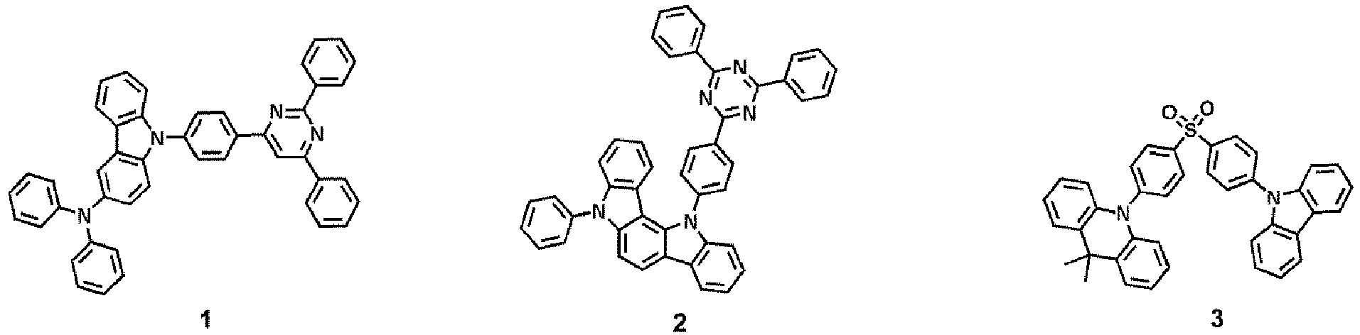


- The host, which is usable in the emission layer together with the TADF emitter, may be selected from any hosts.
- For example, the host may include at least one compound selected from a fluorene-containing compound, a carbazole-containing compound, a dibenzofuran-containing compound, a dibenzothiophene-containing compound, an indenocarbazole-containing compound, an indolocarbazole-containing compound, a benzofurocarbazole-containing compound, a benzothienocarbazole-containing compound, an acridine-containing compound, a dihydroacridine-containing compound, a triindolobenzene-containing compound, a pyridine-containing compound, a pyrimidine-containing compound, a triazine-containing compound, a silicon-containing compound, a cyano group-containing compound, a phosphine oxide-containing compound, a sulfoxide-containing compound, and a sulphonyl-containing compound.
- For example, the host may be a compound including at least one carbazole ring and at least one cyano group or a phosphine oxide-containing compound, but embodiments of the present disclosure are not limited thereto.
- In an embodiment, the host may include at least one compound selected from Compounds H1 to H24, but embodiments of the present disclosure are not limited thereto:


- A ratio of a delayed fluorescence component emitted from the TADF emitter with respect to a total emission component of the emission layer may be about 30% or more (about 33% or more in one example, about 48% or more in another example, about 74% or more in another embodiment).
- An amount of the TADF emitter may be smaller than an amount of the host. For example, an amount of the TADF emitter in the emission layer may be generally selected within a range of about 0.01 parts by weight to about 20 parts by weight based on 100 parts by weight of the emission layer, but embodiments of the present disclosure are not limited thereto. While not wishing to be bound by theory, it is understood that when the amount of the TADF emitter is within this range, light emission may be provided without a quenching phenomenon.
-
FIG. 1 is a schematic view of an organic light-emittingdevice 10 according to an embodiment. Hereinafter, the structure of an organic light-emitting device according to an embodiment and a method of manufacturing an organic light-emitting device according to an embodiment will be described in connection withFIG. 1 . The organic light-emittingdevice 10 includes afirst electrode 11, anorganic layer 15, and asecond electrode 19, which are sequentially stacked. - A substrate may be additionally disposed under the
first electrode 11 or above thesecond electrode 19. For use as the substrate, any substrate that is used in general organic light-emitting devices may be used, and the substrate may be a glass substrate or a transparent plastic substrate, each having excellent mechanical strength, thermal stability, transparency, surface smoothness, ease of handling, and water resistance. - The
first electrode 11 may be formed by depositing or sputtering a material for forming thefirst electrode 11 on the substrate. Thefirst electrode 11 may be an anode. The material for forming thefirst electrode 11 may be selected from materials with a high work function to facilitate hole injection. Thefirst electrode 11 may be a reflective electrode, a semi-transmissive electrode, or a transmissive electrode. The material for forming the first electrode may be, for example, indium tin oxide (ITO), indium zinc oxide (IZO), tin oxide (SnO2), and zinc oxide (ZnO). In one or more embodiments, magnesium (Mg), aluminum (Al), aluminum-lithium (Al-Li), calcium (Ca), magnesium-indium (Mg-In), or magnesium-silver (Mg-Ag) may be used as the material for forming the first electrode. - The
first electrode 11 may have a single-layered structure or a multi-layered structure including two or more layers. For example, thefirst electrode 11 may have a three-layered structure of ITO/Ag/ITO, but the structure of thefirst electrode 110 is not limited thereto. - The
organic layer 15 is disposed on thefirst electrode 11. - The
organic layer 15 may include a hole transport region, an emission layer, and an electron transport region. - The hole transport region may be disposed between the
first electrode 11 and the emission layer. - The hole transport region may include at least one selected from a hole injection layer, a hole transport layer, an electron blocking layer, and a buffer layer.
- The hole transport region may include only either a hole injection layer or a hole transport layer. In one or more embodiments, the hole transport region may have a hole injection layer/hole transport layer structure or a hole injection layer/hole transport layer/electron blocking layer structure, which are sequentially stacked in this stated order from the
first electrode 11. - A hole injection layer may be formed on the
first electrode 11 by using one or more suitable methods selected from vacuum deposition, spin coating, casting, or Langmuir-Blodgett (LB) deposition. - When a hole injection layer is formed by vacuum deposition, the deposition conditions may vary according to a compound that is used to form the hole injection layer, and the structure and thermal characteristics of the hole injection layer. For example, the deposition conditions may include a deposition temperature of about 100°C to about 500°C, a vacuum pressure of about 10-8 torr to about 10-3 torr, and a deposition rate of about 0.01 Å/sec to about 100 Å/sec. However, the deposition conditions are not limited thereto.
- When the hole injection layer is formed using spin coating, coating conditions may vary according to the material used to form the hole injection layer, and the structure and thermal properties of the hole injection layer. For example, a coating speed may be from about 2,000 revolutions per minute (rpm) to about 5,000 rpm, and a temperature at which a heat treatment is performed to remove a solvent after coating may be from about 80°C to about 200°C. However, the coating conditions are not limited thereto.
- Conditions for forming a hole transport layer and an electron blocking layer may be understood by referring to conditions for forming the hole injection layer.
- The hole transport region may include at least one selected from m-MTDATA, TDATA, 2-TNATA, NPB, β-NPB, TPD, spiro-TPD, spiro-NPB, methylated-NPB, TAPC, HMTPD, 4,4',4"-tris(N-carbazolyl)triphenylamine (TCTA), polyaniline/dodecylbenzene sulfonic acid (PANI/DBSA), poly(3,4-ethylenedioxythiophene)/poly(4-styrenesulfonate) (PEDOT/PSS), polyaniline/camphor sulfonic acid (PANI/CSA), polyaniline/poly(4-styrene sulfonate) (PANI/PSS), a compound represented by Formula 201 below, and a compound represented by Formula 202 below:


- a phenylene group, a pentalenylene group, an indenylene group, a naphthylene group, an azulenylene group, a heptalenylene group, an acenaphthylene group, a fluorenylene group, a phenalenylene group, a phenanthrenylene group, an anthracenylene group, a fluoranthenylene group, a triphenylenylene group, a pyrenylene group, a chrysenylenylene group, a naphthacenylene group, a picenylene group, a perylenylene group, and a pentacenylene group; and
- a phenylene group, a pentalenylene group, an indenylene group, a naphthylene group, an azulenylene group, a heptalenylene group, an acenaphthylene group, a fluorenylene group, a phenalenylene group, a phenanthrenylene group, an anthracenylene group, a fluoranthenylene group, a triphenylenylene group, a pyrenylene group, a chrysenylenylene group, a naphthacenylene group, a picenylene group, a perylenylene group, and a pentacenylene group, each substituted with at least one selected from deuterium, -F, -Cl, -Br, -I, a hydroxyl group, a cyano group, a nitro group, an amino group, an amidino group, a hydrazine group, a hydrazone group, a carboxylic acid group or a salt thereof, a sulfonic acid group or a salt thereof, a phosphoric acid group or a salt thereof, a C1-C60 alkyl group, a C2-C60 alkenyl group, a C2-C60 alkynyl group, a C1-C60 alkoxy group, a C3-C10 cycloalkyl group, a C3-C10 cycloalkenyl group, a C1-C10 heterocycloalkyl group, a C1-C10 heterocycloalkenyl group, a C6-C60 aryl group, a C6-C60 aryloxy group, a C6-C60 arylthio group, a C7-C60 arylalkyl group, a C1-C60 heteroaryl group, a C1-C60 heteroaryloxy group, a C1-C60 heteroarylthio group, a C2-C60 heteroarylalkyl group, a monovalent non-aromatic condensed polycyclic group, and a monovalent non-aromatic condensed heteropolycyclic group.
- hydrogen, deuterium, -F, -Cl, -Br, -I, a hydroxyl group, a cyano group, a nitro group, an amino group, an amidino group, a hydrazine group, a hydrazone group, a carboxylic acid group or a salt thereof, a sulfonic acid group or a salt thereof, a phosphoric acid group or a salt thereof, and a C1-C10 alkyl group (for example, a methyl group, an ethyl group, a propyl group, a butyl group, a pentyl group, a hexyl group, and so on), or a C1-C10 alkoxy group (for example, a methoxy group, an ethoxy group, a propoxy group, a butoxy group, a pentoxy group, and so on);
- a C1-C10 alkyl group and a C1-C10 alkoxy group, each substituted with at least one selected from deuterium, -F, -Cl, -Br, -I, a hydroxyl group, a cyano group, a nitro group, an amino group, an amidino group, a hydrazine group, a hydrazone group, a carboxylic acid group or a salt thereof, a sulfonic acid group or a salt thereof, and a phosphoric acid group or a salt thereof;
- a phenyl group, a naphthyl group, an anthracenyl group, a fluorenyl group, and a pyrenyl group; and
- a phenyl group, a naphthyl group, an anthracenyl group, a fluorenyl group, and a pyrenyl group, each substituted with at least one selected from deuterium, -F, -Cl, -Br, -I, a hydroxyl group, a cyano group, a nitro group, an amino group, an amidino group, a hydrazine group, a hydrazone group, a carboxylic acid group or a salt thereof, a sulfonic acid group or a salt thereof, a phosphoric acid group or a salt thereof, a C1-C10 alkyl group, and a C1-C10 alkoxy group,
- but embodiments of the present disclosure are not limited thereto.
- a phenyl group, a naphthyl group, an anthracenyl group, and a pyridinyl group; and
- a phenyl group, a naphthyl group, an anthracenyl group, and a pyridinyl group, each substituted with at least one selected from deuterium, -F, -Cl,-Br, -I, a hydroxyl group, a cyano group, a nitro group, an amino group, an amidino group, a hydrazine group, a hydrazone group, a carboxylic acid group or a salt thereof, a sulfonic acid group or a salt thereof, a phosphoric acid group or a salt thereof, a C1-C20 alkyl group, a C1-C20 alkoxy group, a phenyl group, a naphthyl group, an anthracenyl group, and a pyridinyl group.
- According to an embodiment, the compound represented by Formula 201 may be represented by Formula 201A, but embodiments of the present disclosure are not limited thereto:
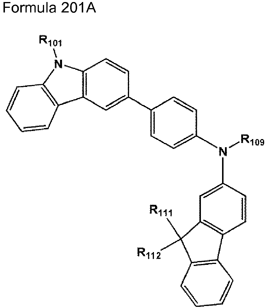
- R101, R111, R112, and R109 in Formula 201A may be understood by referring to the description provided herein.
- For example, the compound represented by Formula 201, and the compound represented by Formula 202 may include compounds HT1 to HT20 illustrated below, but are not limited thereto.


- A thickness of the hole transport region may be in a range of about 100 Å to about 10,000 Å, for example, about 100 Å to about 3,000 Å. When the hole transport region includes at least one of a hole injection layer and a hole transport layer, the thickness of the hole injection layer may be in a range of about 100 Å to about 10,000 Å, for example, about 100 Å to about 2,000 Å, and the thickness of the hole transport layer may be in a range of about 50 Å to about 2,000 Å, for example, about 100 Å to about 1,500 Å. While not wishing to be bound by theory, it is understood that when the thicknesses of the hole transport region, the hole injection layer and the hole transport layer are within these ranges, satisfactory hole transporting characteristics may be obtained without a substantial increase in driving voltage.
- The hole transport region may further include, in addition to these materials, a charge-generation material for the improvement of conductive properties. The charge-generation material may be homogeneously or non-homogeneously dispersed in the hole transport region.
- The charge-generation material may be, for example, a p-dopant. The p-dopant may be one selected from a quinone derivative, a metal oxide, and a cyano group-containing compound, but embodiments of the present disclosure are not limited thereto. Non-limiting examples of the p-dopant are a quinone derivative, such as tetracyanoquinonedimethane (TCNQ) or 2,3,5,6-tetrafluoro-tetracyano-1,4-benzoquinonedimethane (F4-TCNQ); a metal oxide, such as a tungsten oxide or a molybdenium oxide; and a cyano group-containing compound, such as Compound HT-D1 or Compound HT-D2 below, but are not limited thereto.


- The hole transport region may include a buffer layer.
- Also, the buffer layer may compensate for an optical resonance distance according to a wavelength of light emitted from the emission layer, and thus, efficiency of a formed organic light-emitting device may be improved.
- The hole transport region may further include an electron blocking layer. The electron blocking layer may include, for example, mCP, but a material therefor is not limited thereto.

- In one or more embodiments, as an electron blocking material, the host included in the emission layer may be used, but the embodiments are not limited thereto.
- Then, an emission layer may be formed on the hole transport region by vacuum deposition, spin coating, casting, LB deposition, or the like. When the emission layer is formed by vacuum deposition or spin coating, the deposition or coating conditions may be similar to those applied in forming the hole injection layer although the deposition or coating conditions may vary according to a compound that is used to form the emission layer.
- When the organic light-emitting device is a full-color organic light-emitting device, the emission layer may be patterned into a red emission layer, a green emission layer, and a blue emission layer. In one or more embodiments, due to a stacked structure including a red emission layer, a green emission layer, and/or a blue emission layer, the emission layer may emit white light.
- The emission layer may include the TADF emitter and the host described above.
- In one or more embodiments, the emission layer may consist of the TADF emitter and the host described above.
- A thickness of the emission layer may be in a range of about 100 Å to about 1,000 Å, for example, about 200 Å to about 600 Å. While not wishing to be bound by theory, it is understood that when the thickness of the emission layer is within this range, excellent light-emission characteristics may be obtained without a substantial increase in driving voltage.
- Then, an electron transport region may be disposed on the emission layer.
- The electron transport region may include at least one selected from a hole blocking layer, an electron transport layer, and an electron injection layer.
- For example, the electron transport region may have a hole blocking layer/electron transport layer/electron injection layer structure or an electron transport layer/electron injection layer structure, but the structure of the electron transport region is not limited thereto. The electron transport layer may have a single-layered structure or a multi-layered structure including two or more different materials.
- Conditions for forming the hole blocking layer, the electron transport layer, and the electron injection layer which constitute the electron transport region may be understood by referring to the conditions for forming the hole injection layer.
- When the electron transport region includes a hole blocking layer, the hole blocking layer may include, for example, at least one of BCP and Bphen, but may also include other materials.

- In one or more embodiments, as the hole blocking material, a compound that is identical to the host included in the emission layer may be used, but the embodiments are not limited thereto.
- A thickness of the hole blocking layer may be in a range of about 20 Å to about 1,000 Å, for example, about 30 Å to about 300 Å. While not wishing to be bound by theory, it is understood that when the thickness of the hole blocking layer is within these ranges, the hole blocking layer may have improved hole blocking ability without a substantial increase in driving voltage.
- The electron transport layer may include at least one selected from BCP, Bphen, Alq3, BAlq, TAZ, and NTAZ.


- In one or more embodiments, the electron transport layer may include at least one of ET1 to ET25, but are not limited thereto:


- A thickness of the electron transport layer may be in a range of about 100 Å to about 1,000 Å, for example, about 150 Å to about 500 Å. While not wishing to be bound by theory, it is understood that when the thickness of the electron transport layer is within the range described above, the electron transport layer may have satisfactory electron transport characteristics without a substantial increase in driving voltage.
- Also, the electron transport layer may further include, in addition to the materials described above, a metal-containing material.
- The metal-containing material may include a Li complex. The Li complex may include, for example, Compound ET-D1 (lithium 8-hydroxyquinolate, LiQ) or ET-D2.

- The electron transport region may include an electron injection layer that promotes flow of electrons from the
second electrode 19 thereinto. - The electron injection layer may include at least one selected from LiF, NaCl, CsF, Li2O, and BaO.
- A thickness of the electron injection layer may be in a range of about 1 Å to about 100 Å, for example, about 3 Å to about 90 Å. While not wishing to be bound by theory, it is understood that when the thickness of the electron injection layer is within the range described above, the electron injection layer may have satisfactory electron injection characteristics without a substantial increase in driving voltage.
- The
second electrode 19 is disposed on theorganic layer 15. Thesecond electrode 19 may be a cathode. A material for forming thesecond electrode 19 may be selected from metal, an alloy, an electrically conductive compound, and a combination thereof, which have a relatively low work function. For example, lithium (Li), magnesium (Mg), aluminum (Al), aluminum-lithium (Al-Li), calcium (Ca), magnesium-indium (Mg-In), or magnesium-silver (Mg-Ag) may be used as a material for forming thesecond electrode 19. In one or more embodiments, to manufacture a top-emission type light-emitting device, a transmissive electrode formed using ITO or IZO may be used as thesecond electrode 19. - Hereinbefore, the organic light-emitting device has been described with reference to
FIG. 1 , but embodiments of the present disclosure are not limited thereto. - The term "C1-C60 alkyl group" as used herein refers to a linear or branched saturated aliphatic hydrocarbon monovalent group having 1 to 60 carbon atoms, and non-limiting examples thereof include a methyl group, an ethyl group, a propyl group, an iso-butyl group, a sec-butyl group, a tert-butyl group, a pentyl group, an iso-amyl group, and a hexyl group. The term "C1-C60 alkylene group" as used herein refers to a divalent group having the same structure as the C1-C60 alkyl group.
- The term "C1-C60 alkoxy group" as used herein refers to a monovalent group represented by -OA101 (wherein A101 is the C1-C60 alkyl group), and non-limiting examples thereof include a methoxy group, an ethoxy group, and an iso-propyloxy group.
- The term "C2-C60 alkenyl group" as used herein refers to a hydrocarbon group formed by including at least one carbon-carbon double bond in the middle or at the terminus of the C2-C60 alkyl group, and examples thereof include an ethenyl group, a propenyl group, and a butenyl group. The term "C2-C60 alkenylene group" as used herein refers to a divalent group having the same structure as the C2-C60 alkenyl group.
- The term "C2-C60 alkynyl group" as used herein refers to a hydrocarbon group formed by including at least one carbon-carbon triple bond in the middle or at the terminus of the C2-C60 alkyl group, and examples thereof include an ethynyl group, and a propynyl group. The term "C2-C60 alkynylene group" as used herein refers to a divalent group having the same structure as the C2-C60 alkynyl group.
- The term "C3-C10 cycloalkyl group" as used herein refers to a monovalent saturated hydrocarbon monocyclic group having 3 to 10 carbon atoms, and non-limiting examples thereof include a cyclopropyl group, a cyclobutyl group, a cyclopentyl group, a cyclohexyl group, and a cycloheptyl group. The term "C3-C10 cycloalkylene group" as used herein refers to a divalent group having the same structure as the C3-C10 cycloalkyl group.
- The term "C1-C10 heterocycloalkyl group" as used herein refers to a monovalent saturated monocyclic group having at least one heteroatom selected from N, O, P, Si and S as a ring-forming atom and 1 to 10 carbon atoms, and non-limiting examples thereof include a tetrahydrofuranyl group, and a tetrahydrothiophenyl group. The term "C1-C10 heterocycloalkylene group" as used herein refers to a divalent group having the same structure as the C1-C10 heterocycloalkyl group.
- The term "C3-C10 cycloalkenyl group" as used herein refers to a monovalent monocyclic group that has 3 to 10 carbon atoms, at least one carbon-carbon double bond in the ring thereof, and no aromaticity, and non-limiting examples thereof include a cyclopentenyl group, a cyclohexenyl group, and a cycloheptenyl group. The term "C3-C10 cycloalkenylene group" as used herein refers to a divalent group having the same structure as the C3-C10 cycloalkenyl group.
- The term "C1-C10 heterocycloalkenyl group" as used herein refers to a monovalent monocyclic group that has at least one heteroatom selected from N, O, P, Si, and S as a ring-forming atom, 1 to 10 carbon atoms, and at least one carbon-carbon double bond in its ring. Examples of the C1-C10 heterocycloalkenyl group are a 2,3-dihydrofuranyl group, and a 2,3-dihydrothiophenyl group. The term "C1-C10 heterocycloalkenylene group" as used herein refers to a divalent group having the same structure as the C1-C10 heterocycloalkenyl group.
- The term "C6-C60 aryl group" as used herein refers to a monovalent group having a carbocyclic aromatic system having 6 to 60 carbon atoms, and the term "C6-C60 arylene group" as used herein refers to a divalent group having a carbocyclic aromatic system having 6 to 60 carbon atoms. Non-limiting examples of the C6-C60 aryl group include a phenyl group, a naphthyl group, an anthracenyl group, a phenanthrenyl group, a pyrenyl group, and a chrysenyl group. When the C6-C60 aryl group and the C6-C60 arylene group each include two or more rings, the rings may be fused to each other.
- The term "C1-C60 heteroaryl group" as used herein refers to a monovalent group having a heterocyclic aromatic system that has at least one heteroatom selected from N, O, P, and S as a ring-forming atom, and 1 to 60 carbon atoms. The term "C1-C60 heteroarylene group" as used herein refers to a divalent group having a heterocyclic aromatic system that has at least one heteroatom selected from N, O, P, and S as a ring-forming atom, and 1 to 60 carbon atoms. Non-limiting examples of the C1-C60 heteroaryl group include a pyridinyl group, a pyrimidinyl group, a pyrazinyl group, a pyridazinyl group, a triazinyl group, a quinolinyl group, and an isoquinolinyl group. When the C1-C60 heteroaryl group and the C1-C60 heteroarylene group each include two or more rings, the rings may be fused to each other.
- The term "C6-C60 aryloxy group" as used herein indicates -OA102 (wherein A102 is the C6-C60 aryl group), a C6-C60 arylthio group as used herein indicates -SA103 (wherein A103 is the C6-C60 aryl group), and the term "C7-C60 arylalkyl group" as used herein indicates -A104A105 (wherein A104 is the C6-C59 aryl group and A105 is the C1-C53 alkyl group).
- The term "C1-C60 heteroaryloxy group" as used herein refers to -OA106 (wherein A106 is the C2-C60 heteroaryl group), and the term "C1-C60 heteroarylthio group" as used herein indicates -SA107 (wherein A107 is the C2-C60 heteroaryl group).
- The term "C2-C60 heteroarylalkyl group" as used herein refers to -A108A109 (A109 is a C2-C59 heteroaryl group, and A108 is a C1-C58 alkylene group).
- The term "monovalent non-aromatic condensed polycyclic group" as used herein refers to a monovalent group (for example, having 8 to 60 carbon atoms) having two or more rings condensed to each other, only carbon atoms as ring-forming atoms, and no aromaticity in its entire molecular structure. Examples of the monovalent non-aromatic condensed polycyclic group include a fluorenyl group. The term "divalent non-aromatic condensed polycyclic group," as used herein, refers to a divalent group having the same structure as the monovalent non-aromatic condensed polycyclic group.
- The term "monovalent non-aromatic condensed heteropolycyclic group" as used herein refers to a monovalent group (for example, having 2 to 60 carbon atoms) having two or more rings condensed to each other, a heteroatom selected from N, O, P, Si, and S, other than carbon atoms, as a ring-forming atom, and no aromaticity in its entire molecular structure. Non-limiting examples of the monovalent non-aromatic condensed heteropolycyclic group include a carbazolyl group. The term "divalent non-aromatic condensed heteropolycyclic group" as used herein refers to a divalent group having the same structure as the monovalent non-aromatic condensed heteropolycyclic group.
- The term "C5-C30 carbocyclic group" as used herein refers to a saturated or unsaturated cyclic group having, as a ring-forming atom, 5 to 30 carbon atoms only. The C5-C30 carbocyclic group may be a monocyclic group or a polycyclic group.
- The term "C1-C30 heterocyclic group" as used herein refers to a saturated or unsaturated cyclic group having, as a ring-forming atom, at least one heteroatom selected from N, O, Si, P, and S other than 1 to 30 carbon atoms. The C1-C30 heterocyclic group may be a monocyclic group or a polycyclic group.
- At least one substituent of the substituted π electron-depleted nitrogen-containing C2-C60 heterocyclic group, the substituted C3-C10 cycloalkylene group, the substituted C1-C10 heterocycloalkylene group, the substituted C3-C10 cycloalkenylene group, the substituted C1-C10 heterocycloalkenylene group, the substituted C6-C60 arylene group, the substituted C1-C60 heteroarylene group, the substituted divalent non-aromatic condensed polycyclic group, the substituted divalent non-aromatic condensed heteropolycyclic group, the substituted C1-C60 alkyl group, the substituted C2-C60 alkenyl group, the substituted C2-C60 alkynyl group, the substituted C1-C60 alkoxy group, the substituted C3-C10 cycloalkyl group, the substituted C1-C10 heterocycloalkyl group, the substituted C3-C10 cycloalkenyl group, the substituted C1-C10 heterocycloalkenyl group, the substituted C6-C60 aryl group, the substituted C6-C60 aryloxy group, the substituted C6-C60 arylthio group, the substituted C7-C60 arylalkyl group, the substituted C1-C60 heteroaryl group, the substituted C1-C60 heteroaryloxy group, the substituted C1-C60 heteroarylthio group, the substituted C2-C60 heteroarylalkyl group, the substituted monovalent non-aromatic condensed polycyclic group, and the substituted monovalent non-aromatic condensed heteropolycyclic group may be:
- deuterium, -F, -Cl, -Br, -I, a hydroxyl group, a cyano group, a nitro group, an amino group, an amidino group, a hydrazine group, a hydrazone group, a carboxylic acid group or a salt thereof, a sulfonic acid group or a salt thereof,
- a phosphoric acid group or a salt thereof, a C1-C60 alkyl group, a C2-C60 alkenyl group, a C2-C60 alkynyl group, or a C1-C60 alkoxy group;
- a C1-C60 alkyl group, a C2-C60 alkenyl group, a C2-C60 alkynyl group, or a C1-C60 alkoxy group, each substituted with at least one selected from deuterium, -F, -Cl, -Br, -I, a hydroxyl group, a cyano group, a nitro group, an amino group, an amidino group, a hydrazine group, a hydrazone group, a carboxylic acid group or a salt thereof, a sulfonic acid group or a salt thereof, a phosphoric acid group or a salt thereof, a C3-C10 cycloalkyl group, a C1-C10 heterocycloalkyl group, a C3-C10 cycloalkenyl group, a C1-C10 heterocycloalkenyl group, a C6-C60 aryl group, a C6-C60 aryloxy group, a C6-C60 arylthio group, a C7-C60 arylalkyl group, a C1-C60 heteroaryl group, a C1-C60 heteroaryloxy group, a C1-C60 heteroarylthio group, a C2-C60 heteroarylalkyl group, a monovalent non-aromatic condensed polycyclic group, a monovalent non-aromatic condensed heteropolycyclic group,-N(Q11)(Q12), -Si(Q13)(Q14)(Q15), and -B(Q16)(Q17);
- a C3-C10 cycloalkyl group, a C1-C10 heterocycloalkyl group, a C3-C10 cycloalkenyl group, a C1-C10 heterocycloalkenyl group, a C6-C60 aryl group, a C6-C60 aryloxy group, a C6-C60 arylthio group, a C7-C60 arylalkyl group, a C1-C60 heteroaryl group, a C1-C60 heteroaryloxy group, a C1-C60 heteroarylthio group, a C2-C60 heteroarylalkyl group, a monovalent non-aromatic condensed polycyclic group, or a monovalent non-aromatic condensed heteropolycyclic group;
- a C3-C10 cycloalkyl group, a C1-C10 heterocycloalkyl group, a C3-C10 cycloalkenyl group, a C1-C10 heterocycloalkenyl group, a C6-C60 aryl group, a C6-C60 aryloxy group, a C6-C60 arylthio group, a C7-C60 arylalkyl group, a C1-C60 heteroaryl group, a C1-C60 heteroaryloxy group, a C1-C60 heteroarylthio group, a C2-C60 heteroarylalkyl group, a monovalent non-aromatic condensed polycyclic group, or a monovalent non-aromatic condensed heteropolycyclic group, each substituted with at least one selected from deuterium, -F, -Cl,-Br, -I, a hydroxyl group, a cyano group, a nitro group, an amino group, an amidino group, a hydrazine group, a hydrazone group, a carboxylic acid group or a salt thereof, a sulfonic acid group or a salt thereof, a phosphoric acid group or a salt thereof, a C1-C60 alkyl group, a C2-C60 alkenyl group, a C2-C60 alkynyl group, a C1-C60 alkoxy group, a C3-C10 cycloalkyl group, a C1-C10 heterocycloalkyl group, a C3-C10 cycloalkenyl group, a C1-C10 heterocycloalkenyl group, a C6-C60 aryl group, a C6-C60 aryloxy group, a C6-C60 arylthio group, a C7-C60 arylalkyl group, a C1-C60 heteroaryl group, a C1-C60 heteroaryloxy group, a C1-C60 heteroarylthio group, a C2-C60 heteroarylalkyl group, a monovalent non-aromatic condensed polycyclic group, a monovalent non-aromatic condensed heteropolycyclic group, - N(Q21)(Q22), -Si(Q23)(Q24)(Q25), and -B(Q26)(Q27); or -N(Q31)(Q32), -Si(Q33)(Q34)(Q35), or -B(Q36)(Q37), and
- Q11 to Q17, Q21 to Q27, and Q31 to Q37 may each independently be hydrogen, a C1-C60 alkyl group, a C2-C60 alkenyl group, a C2-C60 alkynyl group, a C1-C60 alkoxy group, a C3-C10 cycloalkyl group, a C1-C10 heterocycloalkyl group, a C3-C10 cycloalkenyl group, a C1-C10 heterocycloalkenyl group, a C6-C60 aryl group, a C6-C60 aryloxy group, a C6-C60 arylthio group, a C7-C60 arylalkyl group, a C1-C60 heteroaryl group, a C1-C60 heteroaryloxy group, a C1-C60 heteroarylthio group, a C2-C60 heteroarylalkyl group, a monovalent non-aromatic condensed polycyclic group, or a monovalent non-aromatic condensed heteropolycyclic group.
- The term "room temperature" as used herein refers to about 25°C.
- Hereinafter, an organic light-emitting device according to embodiments are described in detail with reference to. However, the organic light-emitting device is not limited thereto.
- After a quartz substrate cleaned by using chloroform and pure water was prepared, materials shown in Table 1 were vacuum-deposited (co-deposited) at a vacuum degree of 10-7 torr to prepare
films Table 1 Film No. Compound used to form film Film 1 Compound 1 and Compound H19 (volume ratio = 15:85)Film 2Compound 2 and Compound H19 (volume ratio = 15:85)Film 3Compound 3 and Compound H19 (volume ratio = 15:85)Film 3 (DPEPO) Compound 3 and DPEPO (volume ratio = 15:85)Film 4Compound 4 and Compound H19 (volume ratio = 15:85)Film A Compound A and Compound H19 (volume ratio = 15:85) Film A (DPEPO) Compound A and DPEPO (volume ratio = 15:85) Film B Compound B and Compound H19 (volume ratio = 15:85) Film B (DPEPO) Compound B and DPEPO (volume ratio = 15:85) 


- Then, photoluminescence (PL) spectra of the
films FIG. 2 (PL spectrum of the film 1),FIG. 3 (PL spectrum of the film 2),FIG. 4 (PL spectra of thefilm 3 and the film 3 (DPEPO)),FIG. 5 (PL spectrum of the film 4),FIG. 6 (PL spectra of the film A and the film A (DPEPO)), andFIG. 7 (PL spectra of the film B and the film B (DPEPO)), and whether each film satisfies Condition 1-1 or Condition 1-2 are shown in Table 2.Table 2 Film No. Whether a film satisfies Condition 1-1 Whether a film satisfies Condition 1-2 Film 1○ - Film 2○ - Film 3 X ○ (I1/I2) x 100 = 105% I1 = emission intensity at the shortest peak emission wavelength (440nm) in the PL spectrum of the film 3 I2 = emission intensity at the shortest peak emission wavelength (440nm) in the PL spectrum of the film 3 (DPEPO) Film 4○ - Film A X X (I1/I2) x 100 = 127% I1 = emission intensity at the shortest peak emission wavelength (435nm) in the PL spectrum of the film A I2 = emission intensity at the shortest peak emission wavelength (435nm) in the PL spectrum of the film A (DPEPO) Film B X X (I1/I2) x 100 = 292% I1 = emission intensity at the shortest peak emission wavelength (437nm) in the PL spectrum of the film B I2 = emission intensity at the same emission wavelength (437nm) as the shortest peak emission wavelength of the PL spectrum of the film B in the PL spectrum of B (DPEPO) - Referring to Table 2, it is confirmed that, since the
films 1 to 4 satisfies one of Condition 1-1 and Condition 1-2 but the films A and B do not satisfy both Condition 1-1 and Condition 1-2,Compounds 1 to 4 used in thefilms 1 to 4 are excellent TADF emitters, in which dual fluorescence is prevented, and Compounds A and B used in the films A and B have poor TADF characteristics. - Regarding each of
Compounds 1 to 4 and Compounds A and B, with respect to rotamer (10x°) for an integer x satisfying -18 ≤ x ≤ 18, - 1) attachment-detachment overlap density (see
FIGS. 8 to 13 ) - 2) rotational conformational energy (see graphs indicated by "Erc" in
FIGS. 14 to 18 ) - 3) LEosc (oscillator strength in a locally excited state of the rotamer (10x°)) (see graphs indicated by "LEosc" in
FIGS. 14 to 18 ), and - 4) CTosc (oscillator strength in a charge transfer state of the rotamer (10x°)) (see graphs indicated by "CTosc" in
FIGS. 14 to 18 ) - First, the attachment-detachment overlap densities of the each rotamers (10x°) of
Compounds 1 to 4 and Compounds A and B are shown in Table 3 with reference toFIGS. 8 to 13 .Table 3 Compound No. Range including 10x at which the attachment-detachment overlap density of the corresponding rotamer(10x°) is 0.65 or more Whether Compound satisfies Condition 2-11 1 -180 ∼ -170 X -130 ∼ 0 40 ∼ 180 2 -130 ∼ -50 X 50 ∼ 130 3 None ○ 4 -140 ∼ -40 X 40 ∼ 140 A -130 ∼ -20 X 60 ∼ 160 B -180 ∼ 180 X 1: a condition that attachment-detachment overlap densities of all rotamer(10x°) are less than 0.65 - Referring to Table 3, it is confirmed that
Compound 3 satisfies Condition 2-1. - Then, whether
Compounds FIGS. 14 to 18 showing rotational conformational energy, LEosc (oscillator strength in a locally excited state of the rotamer (10x°)), and CTosc (oscillator strength in a charge transfer state of the rotamer (10x°)) for the corresponding rotamer (10x°) of each ofCompounds FIGS. 14 to 18 indicate a range including 10x at which the attachment-detachment overlap density of the corresponding rotamer(10x°) is 0.65 or more.Table 4 Compound No. Range including 10x at which the attachment-detachment overlap density of the rotamer(10x°) is 0.65 or more Whether Compound satisfies Condition 2-2 1 -180 ∼ -170 ○ -130 ∼ 0 40 ∼ 180 2 -130 ∼ -50 ○ 50 ∼ 130 4 -140 ∼ -40 ○ 40 ∼ 140 A -130 ∼ -20 X (Sections A1 to A5 not satisfying Condition 2-2 are present) 60 ∼ 160 B -180 ∼ 180 X (Sections B1 to B3 not satisfying Condition 2-2 are present) - Referring to Table 4, it is confirmed that
Compounds - Referring to
FIGS. 3 and4 , it is confirmed thatCompound 3 satisfies Condition 2-1 andCompounds - PL spectra of the
films - Tdecay(Ex) of the
films Equation 1, and the greatest value of Tdecay obtained from the exponential decay functions used in fitting was taken as Tdecay(Ex). The other Tdecay values may be used to determine a lifetime of a general fluorescence decay lifetime. In this case, a baseline or background signal curve was obtained by repeating the same measurement once more in a dark state (a state in which a pumping signal incident on the film was blocked) for the same time as the measurement time for obtaining the TRPL curve, and the obtained a baseline or background signal curve was used as a baseline in fitting. - Then, a ratio of a delayed fluorescence component with respect to a total emission component was evaluated by calculating a ratio of a value obtained by integrating an exponential decay curve (= change in intensity based on time) determined by Tdecay(Ex) to entire emission intensity integral value according to time. Evaluation results are shown in Table 5.

Table 5 Film No. Ratio of delayed fluorescence component with respect to a total emission component (%) Film 133.9 Film 274.3 Film 330.7 Film 448.6 Film A 4.4 Film B 10.8 - Referring to Table 5, it is determined that the
films 1 to 4 respectively includingCompounds 1 to 4 as an emitter have excellent delayed fluorescence characteristics, as compared with those of the films A and B respectively including Compounds A and B as an emitter. - Photoluminescent quantum yields in the
films Table 6 Film No. PLQY in film Film 1 0.735 Film 20.782 Film 40.531 Film A 0.425 Film B 0.147 - Referring to Table 6, it is confirmed that the
films Compounds - As an anode, a glass substrate, on which an ITO electrode was formed, was cut to a size of 50 mm x 50 mm x 0.5 mm (mm = millimeter), sonicated with acetone, iso-propyl alcohol, and pure water each for 15 minutes, and then cleaned by exposure to ultraviolet (UV) rays and ozone for 30 minutes.
- Then, Compound HT3 and HT-D2 (a concentration of HT-D2 was 3 percent by weight, wt%) were co-deposited on the anode to form a hole injection layer having a thickness of 100 Å, Compound HT3 was deposited on the hole injection layer to form a hole transport layer having a thickness of 1,500 Å, and mCP was deposited on the hole transport layer to form an electron blocking layer having a thickness of 100 Å, thereby forming a hole transport region having a thickness of 1,700 Å.
- Compound H19 (host) and Compound 1 (dopant) were co-deposited on the hole transport region at a volume ratio of 9:1 to form an emission layer having a thickness of 400 Å.
- Compound H19 was vacuum-deposited on the emission layer to form a hole blocking layer having a thickness of 100 Å, Compound ET17 and LiQ were co-deposited on the hole blocking layer at a weight ratio of 5:5 to form an electron transport layer having a thickness of 360 Å, LiQ was deposited on the electron transport layer to form an electron injection layer having a thickness of 5 Å, and Al was vacuum-deposited on the electron injection layer to form a cathode having a thickness of 120 Å, thereby completing the manufacture of an organic light-emitting device.
- Organic light-emitting devices were manufactured in the same manner as in Example 1, except that Compounds shown in Table 7 were each used as a dopant in forming an emission layer.
- The maximum emission wavelength and the maximum external quantum efficiency of the organic light-emitting devices manufactured according to Examples 1 to 3 and Comparative Examples A and B were measured by using a current-voltage meter (Keithley 2400) and a luminance meter (Minolta Cs-1000A). Results thereof are shown in Table 7.
Table 7 Host Dopant Maximum emission wavelength (nm) Maximum external quantum efficiency (EQE) (%) Example 1 H19 1 500 16.8 Example 2 H19 2 484 15.6 Example 3 H19 4 472 14.8 Comparative Example A H19 A 444 4.2 Comparative Example B H19 B 444 2.8 


- Referring to Table 7, it is determined that the organic light-emitting devices of Examples 1 to 3 have improved maximum external quantum efficiency, as compared with those of the organic light-emitting devices of Comparative Examples A and B.
- According to one or more embodiments, since an organic light-emitting device including a TADF emitter satisfying Condition 1-1 or Condition 1-2 may have excellent delayed fluorescence characteristics, regardless of a type of a host used together in an emission layer, the organic light-emitting device including the TADF emitter may have excellent characteristics in terms of quantum efficiency and roll-off ratio.
- It should be understood that embodiments described herein should be considered in a descriptive sense only and not for purposes of limitation. Descriptions of features or aspects within each embodiment should typically be considered as available for other similar features or aspects in other embodiments.
- While one or more embodiments have been described with reference to the figures, it will be understood by those of ordinary skill in the art that various changes in form and details may be made therein without departing from the scope of the present disclosure as defined by the following claims.
Claims (15)
- An organic light-emitting device comprising:a first electrode;a second electrode facing the first electrode; andan organic layer that is disposed between the first electrode and the second electrode, wherein the organic layer comprises an emission layer,wherein the emission layer comprises a thermally activated delayed fluorescence (TADF) emitter and a host and the TADF emitter is different from the host,the TADF emitter satisfies Condition 1-1 or Condition 1-2:Condition 1-1
a condition that n1 is one, andCondition 1-2
a condition that, when n1 is two or more, (I1 / I2) x 100(%) is less than 110%, wherein, in Condition 1-1 and Condition 1-2,I1 (arbitrary units) is emission intensity at the shortest peak emission wavelength in a photoluminescence spectrum 1,1) when n2 is one, I2 (arbitrary units) is emission intensity at the same emission wavelength as the shortest peak emission wavelength of the photoluminescence spectrum 1 in the photoluminescence spectrum 2, and 2) when n2 is two or more, I2 (arbitrary units) is emission intensity at the shortest peak emission wavelength in a photoluminescence spectrum 2,the photoluminescence spectrum 1 is a photoluminescence spectrum of a film 1 that is doped with 15 percent by volume of the TADF emitter in a matrix with the host comprised in the emission layer and has a thickness of 50 nanometers, andthe photoluminescence spectrum 2 is a photoluminescence spectrum of a film 2 that is doped with 15 percent by volume of the TADF emitter in a matrix with DPEPO and has a thickness of 50 nanometers:
- The organic light-emitting device of claim 1, wherein
the TADF emitter is a compound represented by Formula 1:
Formula 1 R1-(D2)d1-D1-(L1)a1-A1,
wherein, in Formula 1,L1 is selected from:a single bond, a cyclopentane group, a cyclohexane group, a cycloheptane group, a cyclooctane group, a cyclopenpentene group, a cyclohexene group, a cycloheptene group, a benzene group, a naphthalene group, a fluorene group, a phenanthrene group, an anthracene group, a fluoranthene group, a triphenylene group, a pyrene group, a chrysene group, a pyrrole group, a thiophene group, a furan group, an imidazole group, a pyrazole group, a thiazole group, an isothiazole group, an oxazole group, an isoxazole group, a pyridine group, a pyrazine group, a pyrimidine group, a pyradizine group, an isoindole group, an indole group, an indazole group, a purine group, a quinoline group, an isoquinoline group, a benzoquinoline group, a quinoxaline group, a quinazoline group, a cinnoline group, a phenanthroline group, a benzimidazole group, a benzofuran group, a benzothiophene group, a benzoxazole group, an isobenzoxazole group, a triazole group, a tetrazole group, an oxadiazole group, a triazine group, a dibenzofuran group, a dibenzothiophene group, a benzocarbazole group, a dibenzocarbazole group, an imidazopyridine group, an imidazopyrimidine group, an azaindole group, an azaindene group, an azabenzofuran group, an azabenzothiophene group, an azacarbazole group, an azafluorene group, an azadibenzofuran group, and an azadibenzothiophene group; anda cyclopentane group, a cyclohexane group, a cycloheptane group, a cyclooctane group, a cyclopenpentene group, a cyclohexene group, a cycloheptene group, a benzene group, a naphthalene group, a fluorene group, a phenanthrene group, an anthracene group, a fluoranthene group, a triphenylene group, a pyrene group, a chrysene group, a pyrrole group, a thiophene group, a furan group, an imidazole group, a pyrazole group, a thiazole group, an isothiazole group, an oxazole group, an isoxazole group, a pyridine group, a pyrazine group, a pyrimidine group, a pyradizine group, an iso-indole group, an indole group, an indazole group, a purine group, a quinoline group, an isoquinoline group, a benzoquinoline group, a quinoxaline group, a quinazoline group, a cinnoline group, a phenanthroline group, a benzimidazole group, a benzofuran group, a benzothiophene group, a benzoxazole group, an isobenzoxazole group, a triazole group, a tetrazole group, an oxadiazole group, a triazine group, a dibenzofuran group, a dibenzothiophene group, a benzocarbazole group, a dibenzocarbazole group, an imidazopyridine group, an imidazopyrimidine group, an azaindole group, an azaindene group, an azabenzofuran group, an azabenzothiophene group, an azacarbazole group, an azafluorene group, an azadibenzofuran group, and an azadibenzothiophene group, each substituted with at least one selected from deuterium, -F, -Cl, -Br, -I, -CD3, - CD2H, -CDH2, -CF3, -CF2H, -CFH2, a hydroxyl group, a cyano group, a nitro group, an amino group, an amidino group, a hydrazine group, a hydrazone group, a carboxylic acid group or a salt thereof, a sulfonic acid group or a salt thereof, a phosphoric acid group or a salt thereof, a C1-C20 alkyl group, a C1-C20 alkoxy group, a phenyl group, a (C1-C20 alkyl)phenyl group, a di(C1-C20 alkyl)phenyl group, a tri(C1-C20 alkyl)phenyl group, a (C6-C20 aryl)phenyl group, a di(C6-C20 aryl)phenyl group, a tri(C6-C20 aryl)phenyl group, a (C3-C20 heteroaryl)phenyl group, a di(C3-C20 heteroaryl)phenyl group, a pyridinyl group, a (C1-C20 alkyl)pyridinyl group, a di(C1-C20 alkyl)pyridinyl group, a (C6-C20 aryl)pyridinyl group, a di(C6-C20 aryl)pyridinyl group, a (C3-C20 heteroaryl)pyridinyl group, a di(C3-C20 heteroaryl)pyridinyl group, a pyrimidinyl group, a (C1-C20 alkyl)pyrimidinyl group, a di(C1-C20 alkyl)pyrimidinyl group, a (C6-C20 aryl)pyrimidinyl group, a di(C6-C20 aryl)pyrimidinyl group, a (C3-C20 heteroaryl)pyrimidinyl group, a di(C3-C20 heteroaryl)pyrimidinyl group, a triazinyl group, a (C1-C20 alkyl)triazinyl group, a di(C1-C20 alkyl)triazinyl group, a (C6-C20 aryl)triazinyl group, a di(C6-C20 aryl)triazinyl group, a (C3-C20 heteroaryl)triazinyl group, and a di(C3-C20 heteroaryl)triazinyl group,a1 is an integer from 1 to 5,D1 and D2 are each an electron donor group,d1 is an integer from 0 to 5,A1 is an electron acceptor group, andR1 is selected from:hydrogen, deuterium, a C1-C60 alkyl group, a C2-C60 alkenyl group, a C2-C60 alkynyl group, a C1-C60 alkoxy group, a C5-C60 carbocyclic group, and a π electron-depleted nitrogen-free C2-C60 heterocyclic group; anda C1-C60 alkyl group, a C2-C60 alkenyl group, a C2-C60 alkynyl group, a C1-C60 alkoxy group, a C5-C60 carbocyclic group, and a π electron-depleted nitrogen-free C2-C60 heterocyclic group, each substituted with at least one selected from deuterium, a C1-C60 alkyl group, a C2-C60 alkenyl group, a C2-C60 alkynyl group, a C1-C60 alkoxy group, a C5-C60carbocyclic group, a (C1-C10 alkyl)C5-C60carbocyclic group, a di(C1-C10 alkyl)C5-C60 carbocyclic group, a (phenyl)C5-C60 carbocyclic group, a di(phenyl)C5-C60 carbocyclic group, a (biphenyl)C5-C60 carbocyclic group, a di(biphenyl)C5-C60 carbocyclic group, a π electron-depleted nitrogen-free C2-C60 heterocyclic group, a (C1-C10 alkyl) π electron-depleted nitrogen-free C2-C60 heterocyclic group, a di(C1-C10 alkyl) π electron-depleted nitrogen-free C2-C60 heterocyclic group, a (phenyl) π electron-depleted nitrogen-free C2-C60 heterocyclic group, a di(phenyl) π electron-depleted nitrogen-free C2-C60 heterocyclic group, a (biphenyl) π electron-depleted nitrogen-free C2-C60 heterocyclic group, and a di(biphenyl) π electron-depleted nitrogen-free C2-C60 heterocyclic group,provided that,i) d1 is an integer from 1 to 5; orii) when d1 is zero, A1 is selected from groups represented by Formulae 3-6(1), 3-10(8), and 3-12(24): wherein, in Formulae 3-6(1), 3-10(8), and 3-12(24),X41 is N(R41), C(R42)(R43), O, or S,R31, R32, R34 to R37 and R41 to R43 are each independently selected from hydrogen, deuterium, -F, -Cl, -Br, -I, -CD3, -CD2H, -CDH2, -CF3, -CF2H, -CFH2, a hydroxyl group, a cyano group, a nitro group, an amino group, an amidino group, a hydrazine group, a hydrazone group, a carboxylic acid group or a salt thereof, a sulfonic acid group or a salt thereof, a phosphoric acid group or a salt thereof, a C1-C20 alkyl group, a C1-C20 alkoxy group, a phenyl group, a (C1-C20 alkyl)phenyl group, a di(C1-C20 alkyl)phenyl group, a tri(C1-C20 alkyl)phenyl group, a (C6-C20 aryl)phenyl group, a di(C6-C20 aryl)phenyl group, a tri(C6-C20 aryl)phenyl group, a (C3-C20 heteroaryl)phenyl group, a di(C3-C20 heteroaryl)phenyl group, a pyridinyl group, a (C1-C20 alkyl)pyridinyl group, a di(C1-C20 alkyl)pyridinyl group, a (C6-C20 aryl)pyridinyl group, a di(C6-C20 aryl)pyridinyl group, a (C3-C20 heteroaryl)pyridinyl group, a di(C3-C20 heteroaryl)pyridinyl group, a pyrimidinyl group, a (C1-C20 alkyl)pyrimidinyl group, a di(C1-C20 alkyl)pyrimidinyl group, a (C6-C20 aryl)pyrimidinyl group, a di(C6-C20 aryl)pyrimidinyl group, a (C3-C20 heteroaryl)pyrimidinyl group, a di(C3-C20 heteroaryl)pyrimidinyl group, a triazinyl group, a (C1-C20 alkyl)triazinyl group, a di(C1-C20 alkyl)triazinyl group, a (C6-C20 aryl)triazinyl group, a di(C6-C20 aryl)triazinyl group, a (C3-C20 heteroaryl)triazinyl group, and a di(C3-C20 heteroaryl)triazinyl group, and* indicates a binding site to a neighboring atom.
 - The organic light-emitting device of claims 1 or 2, wherein
the TADF emitter satisfies Condition 2-1, when assuming that rotamer (0°) is a molecular structure that the TADF emitter has in a gas-phase isolated molecular state, a constant α is an angle between a first plane including D1 and a second plane including A1 in the rotamer (0°), rotamer (10x°) is a molecular structure that the TADF emitter has in a state in which the angle between the first plane and the second plane is changed to α + 10x°, and x is an integer satisfying -18 ≤ x ≤ 18:Condition 2-1
a condition that attachment-detachment overlap densities of the rotamer (10x°) are all less than 0.65. - The organic light-emitting device of claims 1 or 2, wherein
the TADF emitter satisfies Condition 2-2, when assuming that rotamer (0°) is a molecular structure that the TADF emitter has in a gas-phase isolated molecular state, a constant α is an angle between a first plane including D1 and a second plane including A1 in the rotamer (0°), rotamer (10x°) is a molecular structure that the TADF emitter has in a state in which the angle between the first plane and the second plane is changed to α + 10x°, and x is an integer satisfying -18 ≤ x ≤ 18:Condition 2-2wherein, in Condition 2-2, LEosc is oscillator strength in a locally excited state of the corresponding rotamer (10x°), and CTosc is oscillator strength in a charge transfer state of the corresponding rotamer (10x°).
a condition that at least one 10x, of which an attachment-detachment overlap density of the rotamer (10x°) is 0.65 or more, is present, and rotamer (10x°) for all values 10x, of which an attachment-detachment overlap density of rotamer (10x°) is 0.65 or more, have i) rotational conformational energy of 0.15 electron volts or more, ii) CTosc greater than LEosc, or iii) rotational conformationl energy of 0.15 electron volts or more and CTosc greater than LEosc, - The organic light-emitting device of any of claims 2-4, wherein
L1 is selected from:a single bond, a benzene group, a naphthalene group, a fluorene group, a pyridine group, a pyrazine group, a pyrimidine group, a pyradizine group, a quinoline group, an isoquinoline group, a benzoquinoline group, a quinoxaline group, a quinazoline group, and a triazine group; anda benzene group, a naphthalene group, a fluorene group, a pyridine group, a pyrazine group, a pyrimidine group, a pyradizine group, a quinoline group, an isoquinoline group, a benzoquinoline group, a quinoxaline group, a quinazoline group, and a triazine group, each substituted with at least one selected from deuterium, -F, -Cl, -Br, -I, -CD3, -CD2H, -CDH2, -CF3, -CF2H, -CFH2, a hydroxyl group, a cyano group, a nitro group, an amino group, an amidino group, a hydrazine group, a hydrazone group, a carboxylic acid group or a salt thereof, a sulfonic acid group or a salt thereof, a phosphoric acid group or a salt thereof, a C1-C20 alkyl group, a C1-C20 alkoxy group, a phenyl group, a (C1-C20 alkyl)phenyl group, a di(C1-C20 alkyl)phenyl group, a (C6-C20 aryl)phenyl group, a di(C6-C20 aryl)phenyl group, a (C3-C20 heteroaryl)phenyl group, a di(C3-C20 heteroaryl)phenyl group, a pyridinyl group, a (C1-C20 alkyl)pyridinyl group, a di(C1-C20 alkyl)pyridinyl group, a (C6-C20 aryl)pyridinyl group, a di(C6-C20 aryl)pyridinyl group, a (C3-C20 heteroaryl)pyridinyl group, a di(C3-C20 heteroaryl)pyridinyl group, a pyrimidinyl group, a (C1-C20 alkyl)pyrimidinyl group, a di(C1-C20 alkyl)pyrimidinyl group, a (C6-C20 aryl)pyrimidinyl group, a di(C6-C20 aryl)pyrimidinyl group, a (C3-C20 heteroaryl)pyrimidinyl group, a di(C3-C20 heteroaryl)pyrimidinyl group, a triazinyl group, a (C1-C20 alkyl)triazinyl group, a di(C1-C20 alkyl)triazinyl group, a (C6-C20 aryl)triazinyl group, a di(C6-C20 aryl)triazinyl group, a (C3-C20 heteroaryl)triazinyl group, and a di(C3-C20 heteroaryl)triazinyl group, anda1 is 1 or 2. - The organic light-emitting device of any of claims 2-5, wherein
D1 and D2 are each independently selected from groups represented by Formulae 11-1 to 11-4:
 CY1 and CY2 are each independently a C5-C60 carbocyclic group or a C2-C60 heterocyclic group,A11 is selected from:a single bond, a C1-C4 alkylene group, and a C2-C4 alkenylene group; anda C1-C4 alkylene group and a C2-C4 alkenylene group, each substituted with at least one selected from deuterium, a cyano group, a C1-C60 alkyl group, a C1-C60 alkoxy group, a phenyl group, a fluorenyl group, a carbazolyl group, a dibenzofuranyl group, and a dibenzothiophenyl group,R2, R10, and R20 are each independently selected from:hydrogen, deuterium, a C1-C20 alkyl group, a C1-C20 alkoxy group, a cyclopentyl group, a cyclohexyl group, a cycloheptyl group, a cyclopentenyl group, a cyclohexenyl group, a phenyl group, a biphenyl group, a terphenyl group, a pentalenyl group, an indenyl group, a naphthyl group, an azulenyl group, a heptalenyl group, an indacenyl group, an acenaphthyl group, a fluorenyl group, a spiro-bifluorenyl group, a benzofluorenyl group, a dibenzofluorenyl group, a phenalenyl group, a phenanthrenyl group, an anthracenyl group, a fluoranthenyl group, a triphenylenyl group, a pyrenyl group, a chrysenyl group, a naphthacenyl group, a picenyl group, a perylenyl group, a pentaphenyl group, a hexacenyl group, a pentacenyl group, a rubicenyl group, a coronenyl group, an ovalenyl group, a pyrrolyl group, a furanyl group, a thiophenyl group, an indolyl group, a benzofuranyl group, a benzothiophenyl group, a carbazolyl group, a dibenzofuranyl group, a dibenzothiophenyl group, a benzocarbazolyl group, a naphthobenzofuranyl group, a naphthobenzothiophenyl group, a dibenzocarbazolyl group, a dinaphthofuranyl group, a dinaphthothiophenyl group, an indolocarbazolyl group, an indolodibenzofuranyl group, and an indolodibenzothiophenyl group; anda C1-C20 alkyl group, a C1-C20 alkoxy group, a cyclopentyl group, a cyclohexyl group, a cycloheptyl group, a cyclopentenyl group, a cyclohexenyl group, a phenyl group, a biphenyl group, a terphenyl group, a pentalenyl group, an indenyl group, a naphthyl group, an azulenyl group, a heptalenyl group, an indacenyl group, an acenaphthyl group, a fluorenyl group, a spiro-bifluorenyl group, a benzofluorenyl group, a dibenzofluorenyl group, a phenalenyl group, a phenanthrenyl group, an anthracenyl group, a fluoranthenyl group, a triphenylenyl group, a pyrenyl group, a chrysenyl group, a naphthacenyl group, a picenyl group, a perylenyl group, a pentaphenyl group, a hexacenyl group, a pentacenyl group, a rubicenyl group, a coronenyl group, an ovalenyl group, a pyrrolyl group, a furanyl group, a thiophenyl group, an indolyl group, a benzofuranyl group, a benzothiophenyl group, a carbazolyl group, a dibenzofuranyl group, a dibenzothiophenyl group, a benzocarbazolyl group, a naphthobenzofuranyl group, a naphthobenzothiophenyl group, a dibenzocarbazolyl group, a dinaphthofuranyl group, a dinaphthothiophenyl group, an indolocarbazolyl group, an indolodibenzofuranyl group, and an indolodibenzothiophenyl group, each substituted with at least one selected from deuterium, a C1-C20 alkyl group, a C1-C20 alkoxy group, a phenyl group, a biphenyl group, a terphenyl group, a naphthyl group, a fluorenyl group, a dimethylfluorenyl group, a diphenylfluorenyl group, a carbazolyl group, a phenylcarbazolyl group, a biphenylcarbazolyl group, a dibenzofuranyl group, and a dibenzothiophenyl group,b1 and b2 are each independently an integer from 0 to 3, and* and *' each indicate a binding site to a neighboring atom;preferably whereinD1 and D2 are each independently selected from groups represented by Formulae 11(1) to 11 (19):


 X11 is O, S, C(R14), or N(R15)(R16),A11, R2, R10, R20, b1, and b2 are each independently the same as described above,R11 to R16 are each independently the same as described in connection with R10, and* and *' each indicate a binding site to a neighboring atom.
 - The organic light-emitting device of claim 6, wherein
R10 to R16 and R20 are each independently selected from hydrogen, deuterium, a cyano group, a C1-C20 alkyl group, a C1-C20 alkoxy group, a phenyl group, a biphenyl group, a terphenyl group, a naphthyl group, a fluorenyl group, a dimethylfluorenyl group, a diphenylfluorenyl group, a carbazolyl group, a phenylcarbazolyl group, a biphenylcarbazolyl group, a dibenzofuranyl group, and a dibenzothiophenyl group. - The organic light-emitting device of any of claims 2-7, wherein
d1 is 1; and/or
wherein
A1 is selected from a substituted or unsubstituted π electron-depleted nitrogen-containing C2-C60 heterocyclic group and a sulphonyl-containing group. - The organic light-emitting device of any of claims 2-8, wherein
A1 is selected from groups represented by Formulae 3-1 to 3-14 and a sulphonyl-containing group:

 wherein, in Formula 3-1 to 3-14, X31 is N or C(R31), X32 is N or C(R32), X33 is N or C(R33), X34 is N or C(R34), X35 is N or C(R35), X36 is N or C(R36), X37 is N or C(R37), X38 is N or C(R38), and X39 is N or C(R39),X41 in Formulae 3-1, 3-2, and 3-4 to 3-9 is N(R41), C(R42)(R43), O, or S,at least one of X31 to X33 in Formulae 3-1 and 3-2 is N, at least one of X31 to X34 in Formula 3-3 is N, at least one of X31 to X35 in Formulae 3-4, 3-5, and 3-10 is N, at least one of X31 to X37 in Formulae 3-6 to 3-9, 3-11, and 3-12 is N, and at least one of X31 to X39 in Formulae 3-13 and 3-14 is N,R31 to R39 and R41 to R43 are each independently selected from hydrogen, deuterium, -F, -Cl, -Br, -I, -CD3, -CD2H, -CDH2, -CF3, -CF2H, -CFH2, a hydroxyl group, a cyano group, a nitro group, an amino group, an amidino group, a hydrazine group, a hydrazone group, a carboxylic acid group or a salt thereof, a sulfonic acid group or a salt thereof, a phosphoric acid group or a salt thereof, a C1-C20 alkyl group, a C1-C20 alkoxy group, a phenyl group, a (C1-C20 alkyl)phenyl group, a di(C1-C20 alkyl)phenyl group, a tri(C1-C20 alkyl)phenyl group, a (C6-C20 aryl)phenyl group, a di(C6-C20 aryl)phenyl group, a tri(C6-C20 aryl)phenyl group, a (C3-C20 heteroaryl)phenyl group, a di(C3-C20 heteroaryl)phenyl group, a pyridinyl group, a (C1-C20 alkyl)pyridinyl group, a di(C1-C20 alkyl)pyridinyl group, a (C6-C20 aryl)pyridinyl group, a di(C6-C20 aryl)pyridinyl group, a (C3-C20 heteroaryl)pyridinyl group, a di(C3-C20 heteroaryl)pyridinyl group, a pyrimidinyl group, a (C1-C20 alkyl)pyrimidinyl group, a di(C1-C20 alkyl)pyrimidinyl group, a (C6-C20 aryl)pyrimidinyl group, a di(C6-C20 aryl)pyrimidinyl group, a (C3-C20 heteroaryl)pyrimidinyl group, a di(C3-C20 heteroaryl)pyrimidinyl group, a triazinyl group, a (C1-C20 alkyl)triazinyl group, a di(C1-C20 alkyl)triazinyl group, a (C6-C20 aryl)triazinyl group, a di(C6-C20 aryl)triazinyl group, a (C3-C20 heteroaryl)triazinyl group, and a di(C3-C20 heteroaryl)triazinyl group, and* indicates a binding site to a neighboring atom.
 - The organic light-emitting device of any of claims 2-8, wherein
A1 is selected from groups represented by Formulae 3-4(1) to 3-4(4), 3-5(1) to 3-5(4), 3-6(1), 3-7(1), 3-8(1), 3-9(1), 3-10(1) to 3-10(8), 3-11(1) to 3-11 (23), and 3-12(1) to 3-12(24):


 wherein, in Formulae 3-4(1) to 3-4(4), 3-5(1) to 3-5(4), 3-6(1), 3-7(1), 3-8(1), 3-9(1), 3-10(1) to 3-10(8), 3-11 (1) to 3-11 (23), and 3-12(1) to 3-12(24),X41 is N(R41), C(R42)(R43), O, or S,R31 to R37 and R41 to R43 are each independently selected from hydrogen, deuterium, -F, -Cl, -Br, -I, -CD3, -CD2H, -CDH2, -CF3, -CF2H, -CFH2, a hydroxyl group, a cyano group, a nitro group, an amino group, an amidino group, a hydrazine group, a hydrazone group, a carboxylic acid group or a salt thereof, a sulfonic acid group or a salt thereof, a phosphoric acid group or a salt thereof, a C1-C10 alkyl group, a C1-C10 alkoxy group, a phenyl group, a (C1-C10 alkyl)phenyl group, a di(C1-C10 alkyl)phenyl group, a tri(C1-C10 alkyl)phenyl group, a biphenyl group, a di(phenyl)phenyl group, a tri(phenyl)phenyl group, a (pyridinyl)phenyl group, a di(pyridinyl)phenyl group, (pyrimidinyl)phenyl group, a di(pyrimidinyl)phenyl group, a (triazinyl)phenyl group, a di(triazinyl)phenyl group, a (carbazolyl)phenyl group, a pyridinyl group, a (C1-C10 alkyl)pyridinyl group, a di(C1-C10 alkyl)pyridinyl group, a (phenyl)pyridinyl group, a di(phenyl)pyridinyl group, a (pyridinyl)pyridinyl group, a di(pyridinyl)pyridinyl group, a (pyrimidinyl)pyridinyl group, a di(pyrimidinyl)pyridinyl group, a (triazinyl)pyridinyl group, a di(triazinyl)pyridinyl group, a triazinyl group, a (C1-C10 alkyl)triazinyl group, a di(C1-C10 alkyl)triazinyl group, a (phenyl)triazinyl group, a di(phenyl)triazinyl group, (pyridinyl)triazinyl group, a di(pyridinyl)triazinyl group, a (pyrimidinyl)triazinyl group, a di(pyrimidinyl)triazinyl group, a (triazinyl)triazinyl group, and a di(triazinyl)triazinyl group, and* indicates a binding site to a neighboring atom;preferably whereinA1 is selected from Formulae 3-6(1), 3-10(4), 3-10(8), and 3-12(24).
 - The organic light-emitting device of any of claims 2-8, wherein
A1 is a triazine-containing group or a sulphonyl-containing group; and/or
wherein
R1 is selected from hydrogen, deuterium, a cyano group, a C1-C20 alkyl group, a C1-C20 alkoxy group, a phenyl group, a biphenyl group, a terphenyl group, a naphthyl group, a fluorenyl group, a dimethylfluorenyl group, a diphenylfluorenyl group, a carbazolyl group, a phenylcarbazolyl group, a biphenylcarbazolyl group, a dibenzofuranyl group, and a dibenzothiophenyl group. - The organic light-emitting device of any of claims 1-11, wherein
the TADF emitter is selected from Compounds 1 to 11:


whereinthe host comprises at least one compound selected from a fluorene-containing compound, a carbazole-containing compound, a dibenzofuran-containing compound, a dibenzothiophene-containing compound, an indenocarbazole-containing compound, an indolocarbazole-containing compound, a benzofurocarbazole-containing compound, a benzothienocarbazole-containing compound, an acridine-containing compound, a dihydroacridine-containing compound, a triindolobenzene-containing compound, a pyridine-containing compound, a pyrimidine-containing compound, a triazine-containing compound, a silicon-containing compound, a cyano group-containing compound, a phosphine oxide-containing compound, a sulfoxide-containing compound, and a sulphonyl-containing compound. - The organic light-emitting device of any of claims 1-12, wherein
the host is a compound comprising at least one carbazole ring and at least one cyano group or a phosphine oxide-containing compound; or
wherein
the host comprises at least one compound selected from Compounds H1 to H24:


- The organic light-emitting device of any of claims 1-13, wherein a ratio of a delayed fluorescence component emitted from the TADF emitter with respect to a total emission component of the emission layer is 30% or more.
- The organic light-emitting device of any of claims 1-14, wherein
an amount of the TADF emitter is smaller than an amount of the host; and/or
wherein
an amount of the TADF emitter in the emission layer is selected within a range of 0.01 parts by weight to 20 parts by weight based on 100 parts by weight of the emission layer.
Applications Claiming Priority (2)
| Application Number | Priority Date | Filing Date | Title |
|---|---|---|---|
| KR20170026476 | 2017-02-28 | ||
| KR1020180022853A KR20180099521A (en) | 2017-02-28 | 2018-02-26 | Organic light emitting device |
Publications (2)
| Publication Number | Publication Date |
|---|---|
| EP3367456A1 true EP3367456A1 (en) | 2018-08-29 |
| EP3367456B1 EP3367456B1 (en) | 2025-03-26 |
Family
ID=61386766
Family Applications (1)
| Application Number | Title | Priority Date | Filing Date |
|---|---|---|---|
| EP18158782.5A Active EP3367456B1 (en) | 2017-02-28 | 2018-02-27 | Organic light-emitting device |
Country Status (4)
| Country | Link |
|---|---|
| US (1) | US20180248145A1 (en) |
| EP (1) | EP3367456B1 (en) |
| KR (1) | KR20250034054A (en) |
| CN (1) | CN108511613B (en) |
Cited By (2)
| Publication number | Priority date | Publication date | Assignee | Title |
|---|---|---|---|---|
| JP2020172483A (en) * | 2019-04-05 | 2020-10-22 | 三星ディスプレイ株式會社Samsung Display Co.,Ltd. | Compounds for organic electroluminescent devices and organic electroluminescent devices |
| CN112786818A (en) * | 2019-11-07 | 2021-05-11 | 三星显示有限公司 | Organic electroluminescent device and polycyclic compound for organic electroluminescent device |
Families Citing this family (13)
| Publication number | Priority date | Publication date | Assignee | Title |
|---|---|---|---|---|
| WO2016051309A1 (en) | 2014-09-30 | 2016-04-07 | Semiconductor Energy Laboratory Co., Ltd. | Light-emitting element, display device, electronic device, and lighting device |
| CN111372918B (en) | 2018-07-27 | 2023-09-05 | 出光兴产株式会社 | Compound, material for organic electroluminescent element, organic electroluminescent element, and electronic device |
| CN111377908A (en) * | 2018-12-27 | 2020-07-07 | 北京鼎材科技有限公司 | A thermally activated delayed fluorescence compound and its application |
| KR102797542B1 (en) * | 2019-02-13 | 2025-04-21 | 삼성디스플레이 주식회사 | Organic light emitting device |
| FI128701B (en) * | 2019-04-03 | 2020-10-30 | Aalto Univ Foundation Sr | White organic light emitting device and process for production thereof |
| CN110305124B (en) * | 2019-05-24 | 2024-07-30 | 浙江华显光电科技有限公司 | Triazine compound and organic light-emitting device containing same |
| CN110437135A (en) * | 2019-08-12 | 2019-11-12 | 三明学院 | D-A-D ' type fluorescent chemicals and synthesis, application |
| KR102796864B1 (en) * | 2019-08-30 | 2025-04-17 | 삼성전자주식회사 | Organic light emitting device |
| CN110669051A (en) * | 2019-09-30 | 2020-01-10 | 上海天马有机发光显示技术有限公司 | Compound, display panel and display device |
| US11968898B2 (en) * | 2019-10-24 | 2024-04-23 | Lg Display Co., Ltd. | Organic light emitting diode and organic light emitting device including the same |
| TW202142533A (en) * | 2020-04-30 | 2021-11-16 | 日商日鐵化學材料股份有限公司 | Material for organic electroluminescence element, organic electroluminescence element and its manufacturing method, mixed composition |
| KR20210141793A (en) * | 2020-05-12 | 2021-11-23 | 삼성디스플레이 주식회사 | Organic light emitting device and device including the same |
| KR102875303B1 (en) * | 2020-09-28 | 2025-10-22 | 엘지디스플레이 주식회사 | Organic light emitting diode and organic light emitting device including the same |
Citations (4)
| Publication number | Priority date | Publication date | Assignee | Title |
|---|---|---|---|---|
| US20120241732A1 (en) | 2009-12-07 | 2012-09-27 | Ayataka Endo | Organic light-emitting material and organic light-emitting element |
| EP2733762A1 (en) * | 2011-07-15 | 2014-05-21 | Kyushu University, National University Corporation | Organic electroluminescence element and compound used therein |
| US20140138669A1 (en) | 2011-07-15 | 2014-05-22 | Kyushu University National University Corporation | Delayed-fluorescence material and organic electroluminescence element using same |
| EP3020783A1 (en) * | 2014-11-12 | 2016-05-18 | LG Display Co., Ltd. | Delayed fluorescence compound, and organic light emitting diode and display device using the same |
Family Cites Families (9)
| Publication number | Priority date | Publication date | Assignee | Title |
|---|---|---|---|---|
| JP4408367B2 (en) * | 2003-12-22 | 2010-02-03 | 富士フイルム株式会社 | Organic electroluminescence device |
| KR100787425B1 (en) * | 2004-11-29 | 2007-12-26 | 삼성에스디아이 주식회사 | Phenylcarbazole compound and organic electroluminescent device using same |
| KR100752321B1 (en) * | 2005-12-23 | 2007-08-29 | 주식회사 두산 | White Organic Electroluminescent Device |
| KR20130084093A (en) * | 2012-01-16 | 2013-07-24 | 롬엔드하스전자재료코리아유한회사 | Novel organic electroluminescence compounds and organic electroluminescence device using the same |
| KR102304715B1 (en) * | 2013-06-14 | 2021-09-27 | 삼성디스플레이 주식회사 | Organic light emitting diode |
| US10062852B2 (en) * | 2015-06-23 | 2018-08-28 | Samsung Electronics Co., Ltd. | Condensed cyclic compound and organic light-emitting device including the same |
| WO2017014951A1 (en) * | 2015-07-17 | 2017-01-26 | Dow Global Technologies Llc | N-aryl-hydroacridines as light emitting elements for electroluminescent devices |
| CN105924472B (en) * | 2016-04-28 | 2018-04-13 | 黑龙江大学 | Thermal excitation delayed fluorescence blue light guest materials based on triphenyl phosphorus oxygen, preparation method and applications |
| CN106356464B (en) * | 2016-10-24 | 2018-04-17 | 中山大学 | A kind of white light organic electroluminescent device and preparation method thereof |
-
2018
- 2018-02-27 EP EP18158782.5A patent/EP3367456B1/en active Active
- 2018-02-28 US US15/908,150 patent/US20180248145A1/en not_active Abandoned
- 2018-02-28 CN CN201810167020.6A patent/CN108511613B/en active Active
-
2025
- 2025-02-24 KR KR1020250023941A patent/KR20250034054A/en active Pending
Patent Citations (4)
| Publication number | Priority date | Publication date | Assignee | Title |
|---|---|---|---|---|
| US20120241732A1 (en) | 2009-12-07 | 2012-09-27 | Ayataka Endo | Organic light-emitting material and organic light-emitting element |
| EP2733762A1 (en) * | 2011-07-15 | 2014-05-21 | Kyushu University, National University Corporation | Organic electroluminescence element and compound used therein |
| US20140138669A1 (en) | 2011-07-15 | 2014-05-22 | Kyushu University National University Corporation | Delayed-fluorescence material and organic electroluminescence element using same |
| EP3020783A1 (en) * | 2014-11-12 | 2016-05-18 | LG Display Co., Ltd. | Delayed fluorescence compound, and organic light emitting diode and display device using the same |
Non-Patent Citations (3)
| Title |
|---|
| H. UOYAMA ET AL.: "Highly efficient organic light-emitting diodes from delayed fluorescence", NATURE, vol. 492, no. 7428, 13 December 2012 (2012-12-13), pages 234 - 238, XP055048388 |
| IN HO LEE ET AL: "High efficiency blue fluorescent organic light-emitting diodes using a conventional blue fluorescent emitter", JOURNAL OF MATERIALS CHEMISTRY C: MATERIALS FOR OPTICAL AND ELECTRONIC DEVICES, vol. 3, no. 34, 1 January 2015 (2015-01-01), UK, pages 8834 - 8838, XP055488135, ISSN: 2050-7526, DOI: 10.1039/C5TC01626F * |
| RAFAEL GÓMEZ-BOMBARELLI ET AL: "Design of efficient molecular organic light-emitting diodes by a high-throughput virtual screening and experimental approach", NATURE MATERIALS, vol. 15, no. 10, 1 October 2016 (2016-10-01), GB, pages 1120 - 1127, XP055488129, ISSN: 1476-1122, DOI: 10.1038/nmat4717 * |
Cited By (2)
| Publication number | Priority date | Publication date | Assignee | Title |
|---|---|---|---|---|
| JP2020172483A (en) * | 2019-04-05 | 2020-10-22 | 三星ディスプレイ株式會社Samsung Display Co.,Ltd. | Compounds for organic electroluminescent devices and organic electroluminescent devices |
| CN112786818A (en) * | 2019-11-07 | 2021-05-11 | 三星显示有限公司 | Organic electroluminescent device and polycyclic compound for organic electroluminescent device |
Also Published As
| Publication number | Publication date |
|---|---|
| US20180248145A1 (en) | 2018-08-30 |
| CN108511613B (en) | 2022-02-18 |
| CN108511613A (en) | 2018-09-07 |
| KR20250034054A (en) | 2025-03-10 |
| EP3367456B1 (en) | 2025-03-26 |
Similar Documents
| Publication | Publication Date | Title |
|---|---|---|
| EP3367456B1 (en) | Organic light-emitting device | |
| US12167679B2 (en) | Organic light-emitting device | |
| US11713416B2 (en) | Thin film and organic light-emitting device including the same | |
| US12520720B2 (en) | Heterocyclic compound and organic light-emitting device | |
| US10923664B2 (en) | Composition, thin film, and organic light emitting device including composition and thin film | |
| EP3739645B1 (en) | Organic light-emitting device | |
| US10957863B2 (en) | Condensed cyclic compound and organic light-emitting device including the same | |
| US10297764B2 (en) | Mixture, thin film, and organic light emitting device including mixture and thin film | |
| US10510966B2 (en) | Organic light-emitting device | |
| EP3587414B1 (en) | Condensed cyclic compound and organic light-emitting device including the same | |
| EP3211681B1 (en) | Organic light-emitting apparatus | |
| EP3859812B1 (en) | Organic light-emitting device | |
| US20190181353A1 (en) | Organic light-emitting device | |
| EP3588602B1 (en) | Organic light-emitting device | |
| KR20190067694A (en) | Organic light emitting device | |
| EP3787056B1 (en) | Organic light-emitting device | |
| US20170352819A1 (en) | Condensed cyclic compound and organic light-emitting device including the same | |
| EP3598518B1 (en) | Organic light-emitting device | |
| US11124521B2 (en) | Condensed cyclic compound and organic light-emitting device including the same | |
| KR102843325B1 (en) | Organic light emitting device | |
| KR20180099521A (en) | Organic light emitting device | |
| EP4306612B1 (en) | Heterocyclic compound, organic light-emitting device including the same, and electronic apparatus including the organic light-emitting device | |
| US20240415013A1 (en) | Organic electroluminescent element and electronic device |
Legal Events
| Date | Code | Title | Description |
|---|---|---|---|
| PUAI | Public reference made under article 153(3) epc to a published international application that has entered the european phase |
Free format text: ORIGINAL CODE: 0009012 |
|
| STAA | Information on the status of an ep patent application or granted ep patent |
Free format text: STATUS: THE APPLICATION HAS BEEN PUBLISHED |
|
| AK | Designated contracting states |
Kind code of ref document: A1 Designated state(s): AL AT BE BG CH CY CZ DE DK EE ES FI FR GB GR HR HU IE IS IT LI LT LU LV MC MK MT NL NO PL PT RO RS SE SI SK SM TR |
|
| AX | Request for extension of the european patent |
Extension state: BA ME |
|
| STAA | Information on the status of an ep patent application or granted ep patent |
Free format text: STATUS: REQUEST FOR EXAMINATION WAS MADE |
|
| 17P | Request for examination filed |
Effective date: 20190228 |
|
| RBV | Designated contracting states (corrected) |
Designated state(s): AL AT BE BG CH CY CZ DE DK EE ES FI FR GB GR HR HU IE IS IT LI LT LU LV MC MK MT NL NO PL PT RO RS SE SI SK SM TR |
|
| STAA | Information on the status of an ep patent application or granted ep patent |
Free format text: STATUS: EXAMINATION IS IN PROGRESS |
|
| 17Q | First examination report despatched |
Effective date: 20210630 |
|
| P01 | Opt-out of the competence of the unified patent court (upc) registered |
Effective date: 20230530 |
|
| REG | Reference to a national code |
Ref country code: DE Ref legal event code: R079 Free format text: PREVIOUS MAIN CLASS: H01L0051500000 Ipc: H10K0085600000 Ref document number: 602018080405 Country of ref document: DE |
|
| GRAP | Despatch of communication of intention to grant a patent |
Free format text: ORIGINAL CODE: EPIDOSNIGR1 |
|
| STAA | Information on the status of an ep patent application or granted ep patent |
Free format text: STATUS: GRANT OF PATENT IS INTENDED |
|
| RIC1 | Information provided on ipc code assigned before grant |
Ipc: H10K 102/00 20230101ALN20241003BHEP Ipc: H10K 101/20 20230101ALN20241003BHEP Ipc: H10K 50/11 20230101ALN20241003BHEP Ipc: C09K 11/06 20060101ALI20241003BHEP Ipc: H10K 85/60 20230101AFI20241003BHEP |
|
| RIC1 | Information provided on ipc code assigned before grant |
Ipc: H10K 102/00 20230101ALN20241015BHEP Ipc: H10K 101/20 20230101ALN20241015BHEP Ipc: H10K 50/11 20230101ALN20241015BHEP Ipc: C09K 11/06 20060101ALI20241015BHEP Ipc: H10K 85/60 20230101AFI20241015BHEP |
|
| INTG | Intention to grant announced |
Effective date: 20241023 |
|
| GRAS | Grant fee paid |
Free format text: ORIGINAL CODE: EPIDOSNIGR3 |
|
| GRAA | (expected) grant |
Free format text: ORIGINAL CODE: 0009210 |
|
| STAA | Information on the status of an ep patent application or granted ep patent |
Free format text: STATUS: THE PATENT HAS BEEN GRANTED |
|
| AK | Designated contracting states |
Kind code of ref document: B1 Designated state(s): AL AT BE BG CH CY CZ DE DK EE ES FI FR GB GR HR HU IE IS IT LI LT LU LV MC MK MT NL NO PL PT RO RS SE SI SK SM TR |
|
| REG | Reference to a national code |
Ref country code: GB Ref legal event code: FG4D |
|
| REG | Reference to a national code |
Ref country code: CH Ref legal event code: EP |
|
| REG | Reference to a national code |
Ref country code: DE Ref legal event code: R096 Ref document number: 602018080405 Country of ref document: DE |
|
| REG | Reference to a national code |
Ref country code: IE Ref legal event code: FG4D |
|
| REG | Reference to a national code |
Ref country code: DE Ref legal event code: R081 Ref document number: 602018080405 Country of ref document: DE Owner name: SAMSUNG ELECTRONICS CO., LTD., SUWON-SI, KR Free format text: FORMER OWNER: SAMSUNG DISPLAY CO., LTD., YONGIN-SI, GYEONGGI-DO, KR |
|
| PG25 | Lapsed in a contracting state [announced via postgrant information from national office to epo] |
Ref country code: RS Free format text: LAPSE BECAUSE OF FAILURE TO SUBMIT A TRANSLATION OF THE DESCRIPTION OR TO PAY THE FEE WITHIN THE PRESCRIBED TIME-LIMIT Effective date: 20250626 |
|
| PG25 | Lapsed in a contracting state [announced via postgrant information from national office to epo] |
Ref country code: FI Free format text: LAPSE BECAUSE OF FAILURE TO SUBMIT A TRANSLATION OF THE DESCRIPTION OR TO PAY THE FEE WITHIN THE PRESCRIBED TIME-LIMIT Effective date: 20250326 |
|
| REG | Reference to a national code |
Ref country code: LT Ref legal event code: MG9D |
|
| PG25 | Lapsed in a contracting state [announced via postgrant information from national office to epo] |
Ref country code: NO Free format text: LAPSE BECAUSE OF FAILURE TO SUBMIT A TRANSLATION OF THE DESCRIPTION OR TO PAY THE FEE WITHIN THE PRESCRIBED TIME-LIMIT Effective date: 20250626 |
|
| PG25 | Lapsed in a contracting state [announced via postgrant information from national office to epo] |
Ref country code: HR Free format text: LAPSE BECAUSE OF FAILURE TO SUBMIT A TRANSLATION OF THE DESCRIPTION OR TO PAY THE FEE WITHIN THE PRESCRIBED TIME-LIMIT Effective date: 20250326 |
|
| PG25 | Lapsed in a contracting state [announced via postgrant information from national office to epo] |
Ref country code: LV Free format text: LAPSE BECAUSE OF FAILURE TO SUBMIT A TRANSLATION OF THE DESCRIPTION OR TO PAY THE FEE WITHIN THE PRESCRIBED TIME-LIMIT Effective date: 20250326 |
|
| PG25 | Lapsed in a contracting state [announced via postgrant information from national office to epo] |
Ref country code: GR Free format text: LAPSE BECAUSE OF FAILURE TO SUBMIT A TRANSLATION OF THE DESCRIPTION OR TO PAY THE FEE WITHIN THE PRESCRIBED TIME-LIMIT Effective date: 20250627 Ref country code: BG Free format text: LAPSE BECAUSE OF FAILURE TO SUBMIT A TRANSLATION OF THE DESCRIPTION OR TO PAY THE FEE WITHIN THE PRESCRIBED TIME-LIMIT Effective date: 20250326 |
|
| REG | Reference to a national code |
Ref country code: NL Ref legal event code: MP Effective date: 20250326 |
|
| PG25 | Lapsed in a contracting state [announced via postgrant information from national office to epo] |
Ref country code: NL Free format text: LAPSE BECAUSE OF FAILURE TO SUBMIT A TRANSLATION OF THE DESCRIPTION OR TO PAY THE FEE WITHIN THE PRESCRIBED TIME-LIMIT Effective date: 20250326 |
|
| PG25 | Lapsed in a contracting state [announced via postgrant information from national office to epo] |
Ref country code: SE Free format text: LAPSE BECAUSE OF FAILURE TO SUBMIT A TRANSLATION OF THE DESCRIPTION OR TO PAY THE FEE WITHIN THE PRESCRIBED TIME-LIMIT Effective date: 20250326 |
|
| REG | Reference to a national code |
Ref country code: AT Ref legal event code: MK05 Ref document number: 1780314 Country of ref document: AT Kind code of ref document: T Effective date: 20250326 |
|
| PG25 | Lapsed in a contracting state [announced via postgrant information from national office to epo] |
Ref country code: SM Free format text: LAPSE BECAUSE OF FAILURE TO SUBMIT A TRANSLATION OF THE DESCRIPTION OR TO PAY THE FEE WITHIN THE PRESCRIBED TIME-LIMIT Effective date: 20250326 |
|
| PG25 | Lapsed in a contracting state [announced via postgrant information from national office to epo] |
Ref country code: ES Free format text: LAPSE BECAUSE OF FAILURE TO SUBMIT A TRANSLATION OF THE DESCRIPTION OR TO PAY THE FEE WITHIN THE PRESCRIBED TIME-LIMIT Effective date: 20250326 Ref country code: PT Free format text: LAPSE BECAUSE OF FAILURE TO SUBMIT A TRANSLATION OF THE DESCRIPTION OR TO PAY THE FEE WITHIN THE PRESCRIBED TIME-LIMIT Effective date: 20250728 |
|
| PG25 | Lapsed in a contracting state [announced via postgrant information from national office to epo] |
Ref country code: IT Free format text: LAPSE BECAUSE OF FAILURE TO SUBMIT A TRANSLATION OF THE DESCRIPTION OR TO PAY THE FEE WITHIN THE PRESCRIBED TIME-LIMIT Effective date: 20250326 Ref country code: PL Free format text: LAPSE BECAUSE OF FAILURE TO SUBMIT A TRANSLATION OF THE DESCRIPTION OR TO PAY THE FEE WITHIN THE PRESCRIBED TIME-LIMIT Effective date: 20250326 |
|
| PG25 | Lapsed in a contracting state [announced via postgrant information from national office to epo] |
Ref country code: AT Free format text: LAPSE BECAUSE OF FAILURE TO SUBMIT A TRANSLATION OF THE DESCRIPTION OR TO PAY THE FEE WITHIN THE PRESCRIBED TIME-LIMIT Effective date: 20250326 |
|
| PG25 | Lapsed in a contracting state [announced via postgrant information from national office to epo] |
Ref country code: EE Free format text: LAPSE BECAUSE OF FAILURE TO SUBMIT A TRANSLATION OF THE DESCRIPTION OR TO PAY THE FEE WITHIN THE PRESCRIBED TIME-LIMIT Effective date: 20250326 |
|
| PG25 | Lapsed in a contracting state [announced via postgrant information from national office to epo] |
Ref country code: RO Free format text: LAPSE BECAUSE OF FAILURE TO SUBMIT A TRANSLATION OF THE DESCRIPTION OR TO PAY THE FEE WITHIN THE PRESCRIBED TIME-LIMIT Effective date: 20250326 |
|
| PG25 | Lapsed in a contracting state [announced via postgrant information from national office to epo] |
Ref country code: SK Free format text: LAPSE BECAUSE OF FAILURE TO SUBMIT A TRANSLATION OF THE DESCRIPTION OR TO PAY THE FEE WITHIN THE PRESCRIBED TIME-LIMIT Effective date: 20250326 |
|
| PG25 | Lapsed in a contracting state [announced via postgrant information from national office to epo] |
Ref country code: IS Free format text: LAPSE BECAUSE OF FAILURE TO SUBMIT A TRANSLATION OF THE DESCRIPTION OR TO PAY THE FEE WITHIN THE PRESCRIBED TIME-LIMIT Effective date: 20250726 |
|
| REG | Reference to a national code |
Ref country code: DE Ref legal event code: R097 Ref document number: 602018080405 Country of ref document: DE |
|
| PG25 | Lapsed in a contracting state [announced via postgrant information from national office to epo] |
Ref country code: DK Free format text: LAPSE BECAUSE OF FAILURE TO SUBMIT A TRANSLATION OF THE DESCRIPTION OR TO PAY THE FEE WITHIN THE PRESCRIBED TIME-LIMIT Effective date: 20250326 |
|
| PG25 | Lapsed in a contracting state [announced via postgrant information from national office to epo] |
Ref country code: CZ Free format text: LAPSE BECAUSE OF FAILURE TO SUBMIT A TRANSLATION OF THE DESCRIPTION OR TO PAY THE FEE WITHIN THE PRESCRIBED TIME-LIMIT Effective date: 20250326 |
|
| PLBE | No opposition filed within time limit |
Free format text: ORIGINAL CODE: 0009261 |
|
| STAA | Information on the status of an ep patent application or granted ep patent |
Free format text: STATUS: NO OPPOSITION FILED WITHIN TIME LIMIT |
|
| REG | Reference to a national code |
Ref country code: CH Ref legal event code: L10 Free format text: ST27 STATUS EVENT CODE: U-0-0-L10-L00 (AS PROVIDED BY THE NATIONAL OFFICE) Effective date: 20260211 |
|
| 26N | No opposition filed |
Effective date: 20260105 |
|
| PGFP | Annual fee paid to national office [announced via postgrant information from national office to epo] |
Ref country code: GB Payment date: 20260112 Year of fee payment: 9 |
|
| PGFP | Annual fee paid to national office [announced via postgrant information from national office to epo] |
Ref country code: DE Payment date: 20260114 Year of fee payment: 9 |
|
| PGFP | Annual fee paid to national office [announced via postgrant information from national office to epo] |
Ref country code: FR Payment date: 20260108 Year of fee payment: 9 |