EP3367435A2 - Electronic assembly with enhanced thermal dissipation thanks to a metallic bonding layer composed of solder and copper - Google Patents
Electronic assembly with enhanced thermal dissipation thanks to a metallic bonding layer composed of solder and copper Download PDFInfo
- Publication number
- EP3367435A2 EP3367435A2 EP18157432.8A EP18157432A EP3367435A2 EP 3367435 A2 EP3367435 A2 EP 3367435A2 EP 18157432 A EP18157432 A EP 18157432A EP 3367435 A2 EP3367435 A2 EP 3367435A2
- Authority
- EP
- European Patent Office
- Prior art keywords
- metallic
- bonding layer
- semiconductor device
- electronic assembly
- copper
- Prior art date
- Legal status (The legal status is an assumption and is not a legal conclusion. Google has not performed a legal analysis and makes no representation as to the accuracy of the status listed.)
- Granted
Links
Images







Classifications
-
- H—ELECTRICITY
- H10—SEMICONDUCTOR DEVICES; ELECTRIC SOLID-STATE DEVICES NOT OTHERWISE PROVIDED FOR
- H10W—GENERIC PACKAGES, INTERCONNECTIONS, CONNECTORS OR OTHER CONSTRUCTIONAL DETAILS OF DEVICES COVERED BY CLASS H10
- H10W70/00—Package substrates; Interposers; Redistribution layers [RDL]
- H10W70/40—Leadframes
-
- H—ELECTRICITY
- H10—SEMICONDUCTOR DEVICES; ELECTRIC SOLID-STATE DEVICES NOT OTHERWISE PROVIDED FOR
- H10W—GENERIC PACKAGES, INTERCONNECTIONS, CONNECTORS OR OTHER CONSTRUCTIONAL DETAILS OF DEVICES COVERED BY CLASS H10
- H10W70/00—Package substrates; Interposers; Redistribution layers [RDL]
- H10W70/40—Leadframes
- H10W70/461—Leadframes specially adapted for cooling
-
- H—ELECTRICITY
- H10—SEMICONDUCTOR DEVICES; ELECTRIC SOLID-STATE DEVICES NOT OTHERWISE PROVIDED FOR
- H10D—INORGANIC ELECTRIC SEMICONDUCTOR DEVICES
- H10D84/00—Integrated devices formed in or on semiconductor substrates that comprise only semiconducting layers, e.g. on Si wafers or on GaAs-on-Si wafers
- H10D84/80—Integrated devices formed in or on semiconductor substrates that comprise only semiconducting layers, e.g. on Si wafers or on GaAs-on-Si wafers characterised by the integration of at least one component covered by groups H10D12/00 or H10D30/00, e.g. integration of IGFETs
- H10D84/811—Combinations of field-effect devices and one or more diodes, capacitors or resistors
-
- H—ELECTRICITY
- H10—SEMICONDUCTOR DEVICES; ELECTRIC SOLID-STATE DEVICES NOT OTHERWISE PROVIDED FOR
- H10P—GENERIC PROCESSES OR APPARATUS FOR THE MANUFACTURE OR TREATMENT OF DEVICES COVERED BY CLASS H10
- H10P14/00—Formation of materials, e.g. in the shape of layers or pillars
- H10P14/40—Formation of materials, e.g. in the shape of layers or pillars of conductive or resistive materials
-
- H—ELECTRICITY
- H10—SEMICONDUCTOR DEVICES; ELECTRIC SOLID-STATE DEVICES NOT OTHERWISE PROVIDED FOR
- H10W—GENERIC PACKAGES, INTERCONNECTIONS, CONNECTORS OR OTHER CONSTRUCTIONAL DETAILS OF DEVICES COVERED BY CLASS H10
- H10W40/00—Arrangements for thermal protection or thermal control
- H10W40/20—Arrangements for cooling
- H10W40/22—Arrangements for cooling characterised by their shape, e.g. having conical or cylindrical projections
-
- H—ELECTRICITY
- H10—SEMICONDUCTOR DEVICES; ELECTRIC SOLID-STATE DEVICES NOT OTHERWISE PROVIDED FOR
- H10W—GENERIC PACKAGES, INTERCONNECTIONS, CONNECTORS OR OTHER CONSTRUCTIONAL DETAILS OF DEVICES COVERED BY CLASS H10
- H10W40/00—Arrangements for thermal protection or thermal control
- H10W40/20—Arrangements for cooling
- H10W40/25—Arrangements for cooling characterised by their materials
- H10W40/258—Metallic materials
-
- H—ELECTRICITY
- H10—SEMICONDUCTOR DEVICES; ELECTRIC SOLID-STATE DEVICES NOT OTHERWISE PROVIDED FOR
- H10W—GENERIC PACKAGES, INTERCONNECTIONS, CONNECTORS OR OTHER CONSTRUCTIONAL DETAILS OF DEVICES COVERED BY CLASS H10
- H10W40/00—Arrangements for thermal protection or thermal control
- H10W40/70—Fillings or auxiliary members in containers or in encapsulations for thermal protection or control
-
- H—ELECTRICITY
- H10—SEMICONDUCTOR DEVICES; ELECTRIC SOLID-STATE DEVICES NOT OTHERWISE PROVIDED FOR
- H10W—GENERIC PACKAGES, INTERCONNECTIONS, CONNECTORS OR OTHER CONSTRUCTIONAL DETAILS OF DEVICES COVERED BY CLASS H10
- H10W70/00—Package substrates; Interposers; Redistribution layers [RDL]
- H10W70/40—Leadframes
- H10W70/421—Shapes or dispositions
-
- H—ELECTRICITY
- H10—SEMICONDUCTOR DEVICES; ELECTRIC SOLID-STATE DEVICES NOT OTHERWISE PROVIDED FOR
- H10W—GENERIC PACKAGES, INTERCONNECTIONS, CONNECTORS OR OTHER CONSTRUCTIONAL DETAILS OF DEVICES COVERED BY CLASS H10
- H10W90/00—Package configurations
-
- H—ELECTRICITY
- H10—SEMICONDUCTOR DEVICES; ELECTRIC SOLID-STATE DEVICES NOT OTHERWISE PROVIDED FOR
- H10W—GENERIC PACKAGES, INTERCONNECTIONS, CONNECTORS OR OTHER CONSTRUCTIONAL DETAILS OF DEVICES COVERED BY CLASS H10
- H10W40/00—Arrangements for thermal protection or thermal control
- H10W40/20—Arrangements for cooling
- H10W40/231—Arrangements for cooling characterised by their places of attachment or cooling paths
-
- H—ELECTRICITY
- H10—SEMICONDUCTOR DEVICES; ELECTRIC SOLID-STATE DEVICES NOT OTHERWISE PROVIDED FOR
- H10W—GENERIC PACKAGES, INTERCONNECTIONS, CONNECTORS OR OTHER CONSTRUCTIONAL DETAILS OF DEVICES COVERED BY CLASS H10
- H10W72/00—Interconnections or connectors in packages
- H10W72/01—Manufacture or treatment
- H10W72/013—Manufacture or treatment of die-attach connectors
- H10W72/01321—Manufacture or treatment of die-attach connectors using local deposition
- H10W72/01323—Manufacture or treatment of die-attach connectors using local deposition in liquid form, e.g. by dispensing droplets or by screen printing
-
- H—ELECTRICITY
- H10—SEMICONDUCTOR DEVICES; ELECTRIC SOLID-STATE DEVICES NOT OTHERWISE PROVIDED FOR
- H10W—GENERIC PACKAGES, INTERCONNECTIONS, CONNECTORS OR OTHER CONSTRUCTIONAL DETAILS OF DEVICES COVERED BY CLASS H10
- H10W72/00—Interconnections or connectors in packages
- H10W72/071—Connecting or disconnecting
- H10W72/073—Connecting or disconnecting of die-attach connectors
-
- H—ELECTRICITY
- H10—SEMICONDUCTOR DEVICES; ELECTRIC SOLID-STATE DEVICES NOT OTHERWISE PROVIDED FOR
- H10W—GENERIC PACKAGES, INTERCONNECTIONS, CONNECTORS OR OTHER CONSTRUCTIONAL DETAILS OF DEVICES COVERED BY CLASS H10
- H10W72/00—Interconnections or connectors in packages
- H10W72/071—Connecting or disconnecting
- H10W72/073—Connecting or disconnecting of die-attach connectors
- H10W72/07321—Aligning
- H10W72/07323—Active alignment, e.g. using optical alignment using marks or sensors
-
- H—ELECTRICITY
- H10—SEMICONDUCTOR DEVICES; ELECTRIC SOLID-STATE DEVICES NOT OTHERWISE PROVIDED FOR
- H10W—GENERIC PACKAGES, INTERCONNECTIONS, CONNECTORS OR OTHER CONSTRUCTIONAL DETAILS OF DEVICES COVERED BY CLASS H10
- H10W72/00—Interconnections or connectors in packages
- H10W72/071—Connecting or disconnecting
- H10W72/073—Connecting or disconnecting of die-attach connectors
- H10W72/07331—Connecting techniques
- H10W72/07334—Using a reflow oven
-
- H—ELECTRICITY
- H10—SEMICONDUCTOR DEVICES; ELECTRIC SOLID-STATE DEVICES NOT OTHERWISE PROVIDED FOR
- H10W—GENERIC PACKAGES, INTERCONNECTIONS, CONNECTORS OR OTHER CONSTRUCTIONAL DETAILS OF DEVICES COVERED BY CLASS H10
- H10W72/00—Interconnections or connectors in packages
- H10W72/071—Connecting or disconnecting
- H10W72/073—Connecting or disconnecting of die-attach connectors
- H10W72/07331—Connecting techniques
- H10W72/07336—Soldering or alloying
-
- H—ELECTRICITY
- H10—SEMICONDUCTOR DEVICES; ELECTRIC SOLID-STATE DEVICES NOT OTHERWISE PROVIDED FOR
- H10W—GENERIC PACKAGES, INTERCONNECTIONS, CONNECTORS OR OTHER CONSTRUCTIONAL DETAILS OF DEVICES COVERED BY CLASS H10
- H10W72/00—Interconnections or connectors in packages
- H10W72/071—Connecting or disconnecting
- H10W72/073—Connecting or disconnecting of die-attach connectors
- H10W72/07351—Connecting or disconnecting of die-attach connectors characterised by changes in properties of the die-attach connectors during connecting
- H10W72/07352—Connecting or disconnecting of die-attach connectors characterised by changes in properties of the die-attach connectors during connecting changes in structures or sizes
-
- H—ELECTRICITY
- H10—SEMICONDUCTOR DEVICES; ELECTRIC SOLID-STATE DEVICES NOT OTHERWISE PROVIDED FOR
- H10W—GENERIC PACKAGES, INTERCONNECTIONS, CONNECTORS OR OTHER CONSTRUCTIONAL DETAILS OF DEVICES COVERED BY CLASS H10
- H10W72/00—Interconnections or connectors in packages
- H10W72/071—Connecting or disconnecting
- H10W72/073—Connecting or disconnecting of die-attach connectors
- H10W72/07351—Connecting or disconnecting of die-attach connectors characterised by changes in properties of the die-attach connectors during connecting
- H10W72/07354—Connecting or disconnecting of die-attach connectors characterised by changes in properties of the die-attach connectors during connecting changes in dispositions
-
- H—ELECTRICITY
- H10—SEMICONDUCTOR DEVICES; ELECTRIC SOLID-STATE DEVICES NOT OTHERWISE PROVIDED FOR
- H10W—GENERIC PACKAGES, INTERCONNECTIONS, CONNECTORS OR OTHER CONSTRUCTIONAL DETAILS OF DEVICES COVERED BY CLASS H10
- H10W72/00—Interconnections or connectors in packages
- H10W72/30—Die-attach connectors
- H10W72/321—Structures or relative sizes of die-attach connectors
-
- H—ELECTRICITY
- H10—SEMICONDUCTOR DEVICES; ELECTRIC SOLID-STATE DEVICES NOT OTHERWISE PROVIDED FOR
- H10W—GENERIC PACKAGES, INTERCONNECTIONS, CONNECTORS OR OTHER CONSTRUCTIONAL DETAILS OF DEVICES COVERED BY CLASS H10
- H10W72/00—Interconnections or connectors in packages
- H10W72/30—Die-attach connectors
- H10W72/321—Structures or relative sizes of die-attach connectors
- H10W72/325—Die-attach connectors having a filler embedded in a matrix
-
- H—ELECTRICITY
- H10—SEMICONDUCTOR DEVICES; ELECTRIC SOLID-STATE DEVICES NOT OTHERWISE PROVIDED FOR
- H10W—GENERIC PACKAGES, INTERCONNECTIONS, CONNECTORS OR OTHER CONSTRUCTIONAL DETAILS OF DEVICES COVERED BY CLASS H10
- H10W72/00—Interconnections or connectors in packages
- H10W72/30—Die-attach connectors
- H10W72/321—Structures or relative sizes of die-attach connectors
- H10W72/327—Multiple die-attach connectors having different sizes
-
- H—ELECTRICITY
- H10—SEMICONDUCTOR DEVICES; ELECTRIC SOLID-STATE DEVICES NOT OTHERWISE PROVIDED FOR
- H10W—GENERIC PACKAGES, INTERCONNECTIONS, CONNECTORS OR OTHER CONSTRUCTIONAL DETAILS OF DEVICES COVERED BY CLASS H10
- H10W72/00—Interconnections or connectors in packages
- H10W72/30—Die-attach connectors
- H10W72/341—Dispositions of die-attach connectors, e.g. layouts
- H10W72/344—Dispositions of die-attach connectors, e.g. layouts relative to underlying supporting features, e.g. bond pads, RDLs or vias
-
- H—ELECTRICITY
- H10—SEMICONDUCTOR DEVICES; ELECTRIC SOLID-STATE DEVICES NOT OTHERWISE PROVIDED FOR
- H10W—GENERIC PACKAGES, INTERCONNECTIONS, CONNECTORS OR OTHER CONSTRUCTIONAL DETAILS OF DEVICES COVERED BY CLASS H10
- H10W72/00—Interconnections or connectors in packages
- H10W72/30—Die-attach connectors
- H10W72/341—Dispositions of die-attach connectors, e.g. layouts
- H10W72/347—Dispositions of multiple die-attach connectors
-
- H—ELECTRICITY
- H10—SEMICONDUCTOR DEVICES; ELECTRIC SOLID-STATE DEVICES NOT OTHERWISE PROVIDED FOR
- H10W—GENERIC PACKAGES, INTERCONNECTIONS, CONNECTORS OR OTHER CONSTRUCTIONAL DETAILS OF DEVICES COVERED BY CLASS H10
- H10W72/00—Interconnections or connectors in packages
- H10W72/30—Die-attach connectors
- H10W72/351—Materials of die-attach connectors
-
- H—ELECTRICITY
- H10—SEMICONDUCTOR DEVICES; ELECTRIC SOLID-STATE DEVICES NOT OTHERWISE PROVIDED FOR
- H10W—GENERIC PACKAGES, INTERCONNECTIONS, CONNECTORS OR OTHER CONSTRUCTIONAL DETAILS OF DEVICES COVERED BY CLASS H10
- H10W72/00—Interconnections or connectors in packages
- H10W72/30—Die-attach connectors
- H10W72/351—Materials of die-attach connectors
- H10W72/352—Materials of die-attach connectors comprising metals or metalloids, e.g. solders
-
- H—ELECTRICITY
- H10—SEMICONDUCTOR DEVICES; ELECTRIC SOLID-STATE DEVICES NOT OTHERWISE PROVIDED FOR
- H10W—GENERIC PACKAGES, INTERCONNECTIONS, CONNECTORS OR OTHER CONSTRUCTIONAL DETAILS OF DEVICES COVERED BY CLASS H10
- H10W72/00—Interconnections or connectors in packages
- H10W72/30—Die-attach connectors
- H10W72/351—Materials of die-attach connectors
- H10W72/353—Materials of die-attach connectors not comprising solid metals or solid metalloids, e.g. ceramics
-
- H—ELECTRICITY
- H10—SEMICONDUCTOR DEVICES; ELECTRIC SOLID-STATE DEVICES NOT OTHERWISE PROVIDED FOR
- H10W—GENERIC PACKAGES, INTERCONNECTIONS, CONNECTORS OR OTHER CONSTRUCTIONAL DETAILS OF DEVICES COVERED BY CLASS H10
- H10W90/00—Package configurations
- H10W90/701—Package configurations characterised by the relative positions of pads or connectors relative to package parts
- H10W90/731—Package configurations characterised by the relative positions of pads or connectors relative to package parts of die-attach connectors
- H10W90/732—Package configurations characterised by the relative positions of pads or connectors relative to package parts of die-attach connectors between stacked chips
-
- H—ELECTRICITY
- H10—SEMICONDUCTOR DEVICES; ELECTRIC SOLID-STATE DEVICES NOT OTHERWISE PROVIDED FOR
- H10W—GENERIC PACKAGES, INTERCONNECTIONS, CONNECTORS OR OTHER CONSTRUCTIONAL DETAILS OF DEVICES COVERED BY CLASS H10
- H10W90/00—Package configurations
- H10W90/701—Package configurations characterised by the relative positions of pads or connectors relative to package parts
- H10W90/731—Package configurations characterised by the relative positions of pads or connectors relative to package parts of die-attach connectors
- H10W90/734—Package configurations characterised by the relative positions of pads or connectors relative to package parts of die-attach connectors between a chip and a stacked insulating package substrate, interposer or RDL
-
- H—ELECTRICITY
- H10—SEMICONDUCTOR DEVICES; ELECTRIC SOLID-STATE DEVICES NOT OTHERWISE PROVIDED FOR
- H10W—GENERIC PACKAGES, INTERCONNECTIONS, CONNECTORS OR OTHER CONSTRUCTIONAL DETAILS OF DEVICES COVERED BY CLASS H10
- H10W90/00—Package configurations
- H10W90/701—Package configurations characterised by the relative positions of pads or connectors relative to package parts
- H10W90/731—Package configurations characterised by the relative positions of pads or connectors relative to package parts of die-attach connectors
- H10W90/736—Package configurations characterised by the relative positions of pads or connectors relative to package parts of die-attach connectors between a chip and a stacked lead frame, conducting package substrate or heat sink
Definitions
- This disclosure relates to an electronic assembly with enhanced thermal dissipation.
- Certain prior art uses bonded wire to connect the leads of a semiconductor device to a semiconductor package or substrate.
- the thermal dissipation, the operational temperature range, or the maximum operating temperature of the semiconductor device may be limited because of the bonded wire connections.
- Some semiconductor devices may use silicon carbide for its superior power handling capabilities.
- silicon carbide presents challenges in semiconductor packaging with respect to providing adequate thermal dissipation.
- an electronic assembly comprises a semiconductor device with a first side and a second side opposite the first side.
- the first side has a first conductive pad.
- the second side has a primary metallic surface.
- a first substrate e.g. lead frame
- a second substrate e.g., heat sinking circuit board
- the second metallic bonding layer is composed of solder and copper, for example.
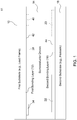
- FIG. 1 is a block diagram that is representative of a cross-section of one embodiment of an electronic assembly 11 of the disclosure.
- an electronic assembly 11 comprises a semiconductor device 14 with a first side 42 and a second side 44 opposite the first side 42.
- the first side 42 has a first conductive pad 34.
- the second side 44 has a primary metallic surface 22.
- a first substrate 10 e.g. lead frame
- a second substrate 18 is bonded to the primary metallic surface 22 via a second metallic bonding layer 16.
- the first bonding layer 12 provides an electrical and mechanical connection between the first conductive pad 34 and the first substrate 10 (e.g., one or more lead frames). Alternatively, the first bonding layer 12 provides a set of respective electrical and mechanical connections to different terminals of a lead frame for a corresponding first conductive pad 34, a corresponding second conductive pad 38 and corresponding third conductive pad 40.
- the second bonding layer 16 provides an electrical and mechanical connection between the primary metallic surface 22 and the second substrate 18 (e.g., heat sink or heat-sinking circuit board). Alternatively, the second bonding layer 16 provides an electrical and mechanical connection between the primary metallic surface 22, the secondary metallic surface 23 and the second substrate (e.g. heat sink or heat sinking circuit board).
- the first bonding layer 12 is composed of solder; the second bonding layer 16 is composed of solder or both solder and copper material. However, in an alternate embodiment, the first bonding layer 12 is composed of both solder and copper material.
- the copper content e.g., copper pellets
- the copper content can facilitate enhanced heat dissipation from the semiconductor device 14. Further, the copper content can promote improved thermomechanical strength of one or more bonding layers (12, 16). For example, in one embodiment, the copper (in the first bonding layer 12) lowers a homologous temperature of the first bonding layer 12 to facilitate greater mechanical strength (e.g., sheer, tensile and/or compressive strength) of a bond between the first bonding layer 12 and the first conductive pad 34.
- the copper (in the second bonding layer 16) lowers a homologous temperature of the second bonding layer 16 to facilitate greater mechanical strength (e.g., sheer, tensile and/or compressive strength) of a bond between the second bonding layer 16 and the primary metallic surface 22.
- mechanical strength e.g., sheer, tensile and/or compressive strength
- the semiconductor device 14 has a primary coefficient of thermal expansion (CTE), whereas the first substrate 10 (e.g., lead frame) or secondary substrate 18 (e.g., heatsink) has a secondary coefficient of thermal expansion (CTE), and wherein the copper in the first bonding layer 12 or the second bonding layer 16, respectively, reduces a mismatch (and associated thermal stress) between the primary CTE and the secondary CTE.
- CTE primary coefficient of thermal expansion
- first substrate 10 e.g., lead frame
- secondary substrate 18 e.g., heatsink
- the semiconductor device 14 further comprises a second conductive pad 38 and a third conductive pad 40 on the first side 42. As shown in FIG. 1 , the second pad 38 and the third conductive pad 40 are optional as indicated by the dashed lines. Similarly, in an alternate embodiment, the semiconductor device 14 further comprises a secondary metallic surface 23, which is optional as indicated by the dashed lines in FIG. 1 .
- any or all of the conductive pads (34, 38, 40) are composed of electrically conductive materials, such as metal (e.g., copper), alloys or metallic materials.
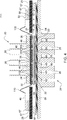
- FIG. 2 is an embodiment of a cross-section of an electronic assembly 111 taken along reference line 2-2 of FIG. 3A and FIG. 3B .
- FIG. 2 shows an illustrative example of one possible cross-section of an electronic assembly 111.
- Like reference numbers in any permutation of FIG. 1 , FIG. 2 , FIG. 3A and FIG. 3B indicate like elements or features.
- the first substrate comprises one or more lead frames 110 for interfacing with at least the first conductive pad 34 on a respective semiconductor device 14.
- the first substrate comprises a plurality of lead frames 110 for interfacing with the corresponding first conductive pads 34 on a corresponding plurality of respective semiconductor devices 14. As illustrated in FIG. 2 , each lead frame 110 engages, interfaces or registers with the corresponding conductive pad 34, the corresponding second conductive pad 38 and corresponding third conductive pad 40 associated with the first side 42 of the semiconductor device 14, such as semiconductor die.
- the first conductive pad 34 may comprise a continuous metallic member (e.g., with a rectangular or polygonal surface area), where a first matrix 112 of solder paste is placed on a grid, array or pattern of islands on the first conductive pad 34;
- the second conductive pad 38 may comprise a continuous metallic member (e.g., with a rectangular or polygonal surface area), where a second matrix 212 of solder paste is placed on a grid, array or pattern of islands on the second conductive pad 38;
- the third conductive pad 40 may comprise a continuous metallic member (e.g., with a rectangular or polygonal surface area), where a third matrix 312 of solder paste is placed on a grid, array or pattern of islands on the third conductive pad 40.
- the solder paste is reflowed during the manufacturing of the assembly 111, for example.
- the first matrix 112 of solder paste, the second matrix 212 of solder paste and the third matrix 312 of solder paste may be
- a set of first conductive pads comprise a grid or array of conductive metallic islands that are spaced apart by a lateral gap (e.g., lateral dielectric gap or air gap) on the first side 42 of the semiconductor device 14.
- a set of second conductive pads comprise a grid or array of conductive metallic islands that are spaced apart by a lateral gap (e.g., lateral dielectric gap or air gap) on the first side 42 of the semiconductor device 14;
- a set of third conductive pads comprise a grid or array of conductive metallic islands that are spaced apart by a lateral gap (e.g., lateral dielectric gap or air gap) on the first side 42 of the semiconductor device 14.
- first, second and third matrices (112, 212, 312) of solder paste are spatially aligned with, and coextensive in size and shape with, the underlying set of first conductive pads, the underlying set of second conductive pads and the underlying set of third conductive pads.
- each lead frame 110 has a substantially planar portion 46 that has a lower surface for interfacing with the first conductive pad 34 on the semiconductor device 14 and an upper surface for coupling or receiving, directly or indirectly, a first heat sink 20. Further, the substantially planar portion 46 may interface with the first conductive pad 34, the second conductive pad 38 and the third conductive pad 40.
- each first bonding layer 12 may interconnect one or more lead frames 110 (via its lower surface) to the corresponding first conductive pad 34, the corresponding second conductive pad 38 and the corresponding third conductive pad 40 of one or more respective semiconductor devices 14.
- first conductive pad 34 is associated with a corresponding first terminal of the semiconductor device 14
- second conductive pad 38 is associated with a corresponding second terminal of the semiconductor device 14
- third conductive pad 40 is associated with a third terminal of the semiconductor device 14, where each terminal represents a distinct node or port (e.g., input or output port) of the semiconductor device 14.
- first terminal comprises an anode of a diode
- the second terminal comprises an emitter or source of a transistor
- the third terminal comprises a base or a gate of the transistor.
- the first bonding layer 12 may comprise a continuous metallic layer (e.g., after reflow of the solder or solder and copper) or may comprise a first matrix 112, a second matrix 212, and a third matrix 312 (e.g., grid or array in one or two dimensions) of discontinuous conductive islands that are spaced apart by at least one lateral air gap or lateral isolation gap to support different leads or terminals for each semiconductor device 14.
- the first terminal or first conductive pad 34 is associated with the respective first matrix 112
- the second terminal or second conductive pad 38 is associated with the respective second matrix 212
- the third terminal or third conductive pad 40 is associated with the third matrix 312.
- a thermal interface layer 36 (e.g., dielectric thermal interface material) or other dielectric layer is disposed between the lead frame 110 (or its upper surface) and the first heat sink 20, or its first base 32.
- the first heat sink 20 has a substantially planar mating surface or first base 32 for adjoining the thermal interface material 36. Fins 26, ridges or other protrusions extend outward from a side of the first heat sink 20 that is opposite the substantially planar mating surface.
- the first substrate comprises a lead frame 110 having a substantially planar portion 46 with a series or grid of holes 54 (in FIG. 5 ) for interfacing with the first bonding layer 12 (e.g., first metallic bonding layer).
- the first substrate comprises a lead frame 110 that is capable of laterally spreading or dissipating heat to reduce any temperature differential within different portions of the electronic assembly 111, or among a plurality of semiconductor devices 14 of the electronic assembly 111.
- the second substrate comprises a second heat sink 24 with a second base 30.
- the second base 30 has a substantially planar surface for interconnection with the primary metallic surface 22, the secondary metallic surface 23, or both, of the one or more semiconductor devices 14.
- the second bonding layer 16 facilitates the interconnection between the second base 30 or second heat sink 24 and the primary metallic surface 22, the secondary metallic surface 23 or both of the one or more semiconductor devices 14. Fins 28, ridges or other protrusions extend outward from a side of the second heat sink 24 that is opposite the substantially planar surface.
- the first bonding layer 12 may comprise one or more of the following matrices of solder paste or a combination of solder paste and copper material: a first matrix 112, a second matrix 212 or a third matrix 312.
- the first bonding layer 12 or first metallic bonding layer is composed of solder material, such as a composition of tin and silver, lead solder, or another suitable lead-free solder material.
- the first bonding layer 12 may comprise a combination of solder and copper material.
- the first bonding layer 12 comprises solder material (e.g., a lead-free solder material) and copper pellets coated with a solderable finish such as tin, silver or electroless nickel immersion gold (ENIG).
- the solder material or solder paste is a lead-free solder material or alloy composition, such as tin-silver, tin-silver-copper, or tin-gold, or tin and one or more other metallic elements, such as antimony, bismuth, indium, or zinc.
- tin-silver-copper solder alloy composition can be composed of approximately 2.5 to 4 percent silver by mass, approximately .25 to 1 percent copper by mass with the remaining mass being tin or a composition of tin.
- the solder powder size range should be: 20-38 microns and the solder paste is 90 percent metal load (percentage-by-weight of solder in the paste).
- solder paste can contain lead, such as tin-silver-lead or tin-lead, if the lead-containing solder material is authorized under applicable law and regulations, such as military specifications.
- copper material or additional copper material is added to the above solder material or alloy composition, such that the copper content may exceed the range of .25 to 1 percent copper by mass of the first bonding layer 12 of the second bonding layer 16.
- embedded copper material in the solder paste can be in the form of discs plated with a solderable finish such as tin, silver, or ENIG, among other possibilities.
- the diameter and thickness of the disc is 0.025 inches (0.
- the second bonding layer 16 may comprise one or more separate islands, bodies, or matrices (e.g., 116 in FIG. 7 ) of solder paste or a composition (e.g., alloy composition) of solder (e.g., lead-free solder, even including up to 1 percent copper by mass) and copper material (e.g., copper particles, copper flakes, copper pellets, or copper filler).
- solder paste or a composition (e.g., alloy composition) of solder (e.g., lead-free solder, even including up to 1 percent copper by mass) and copper material (e.g., copper particles, copper flakes, copper pellets, or copper filler).
- the second bonding layer 16 or second metallic bonding layer is composed of copper material and solder material, such as a composition of tin and silver, lead solder, or another suitable lead-free solder material.
- the copper comprises copper pellets coated with tin, silver, or electroless nickel immersion gold. The copper is well-suited to lower a homologous temperature of the second bonding layer 16 to facilitate greater mechanical strength of a bond between the second bonding layer 16 and the primary metallic surfaces 22.
- the semiconductor device 14 is capable of generating heat
- the first bonding layer 12 and the second bonding layer 16 comprise metallic materials or thermal interface materials that conduct simultaneously the heat away from one or more semiconductor devices 14 from each first side 42 of each semiconductor device 14 and from each second side 44 of each semiconductor device 14 (among the devices).
- the semiconductor device 14 has a primary coefficient of thermal expansion (CTE) and the first substrate 10 (e.g., lead frames 110) or the second substrate 18 (e.g., second heat sink 24) has a secondary coefficient of thermal expansion (CTE); the copper in the first bonding layer 12 or the second bonding layer 16, respectively, reduces a mismatch (and associated thermal stress) between the primary CTE and the secondary CTE.
- CTE primary coefficient of thermal expansion
- the first substrate 10 e.g., lead frames 110
- the second substrate 18 e.g., second heat sink 24
- CTE secondary coefficient of thermal expansion
- the electronic assembly 111 comprises a set of semiconductor devices 14.
- each semiconductor device 14 comprises a semiconductor die, such as an insulated gate bipolar transistor (IGBT) or an insulated gate bipolar transistor and a diode on or in a direct bonded copper carrier or semiconductor substrate.
- IGBT insulated gate bipolar transistor
- Each semiconductor device 14 is capable of generating heat during normal operation.
- the first bonding layer 12 and the second bonding layer 16 comprise thermal interface materials that conduct simultaneously the heat away from the semiconductor device 14 from a first side 42 of the semiconductor device 14 and from a second side 44 of the semiconductor device 14.
- the first substrate comprises one or more lead frames 110 that are capable of laterally spreading or dissipating the heat to reduce any temperature differential within different portions of the electronic assembly 111, or among a plurality of semiconductor devices 14 of the electronic assembly 111.
- the first substrate comprises a lead frame 110 with a substantially planar portion 46 having a lower surface for interfacing with the corresponding first conductive pad 34, second conductive pad 38, and third conductive pad 40 on the semiconductor device 14.
- the substantially planar portion 46 of the lead frame 110 has an upper surface for coupling or receiving, directly or indirectly, a first heat sink 20.
- the upper surface of the substantially planar portion 46 (of the lead frame 110) adjoins the dielectric thermal interface material 36 (e.g., thermally conductive adhesive), which is sandwiched between the upper surface and the first heat sink 20 or its first base 32.
- the lead frame 110 terminates in a first terminal 48 and a second terminal 50, which can be connected to conductive traces 57 on the circuit board 25 via solder joints 67.
- the circuit board 25 has an opening 59 of a size and shape to receive the semiconductor device 14 with a peripheral clearance gap.
- the circuit board 25 may be composed of a ceramic, polymeric, plastic, polymer with glass filler, for example, with conductive traces on one or both sides.
- FIG. 3A is a plan view of a first side 42 (e.g., upper side) of one illustrative embodiment of a semiconductor device 14.
- the first side 42 of the semiconductor device 14 comprises the first conductive pad 34, the second conductive pad 38 and the third conductive pad 40 which are laterally separated from each other by one or more dielectric barriers 145.
- Each dielectric barrier 145 represents an air gap, a ceramic insulating region, a plastic or polymer insulating region, or another dielectric region.
- each first conductive pad 34, each second conductive pad 38 and each third conductive pad 40 is associated with a corresponding lead or terminal of a respective semiconductor device 14.
- any pad (34, 38 and 40) may represent: (1) a gate pad or base pad, (2) an emitter pad or source pad, (3) an anode pad, or (4) a cathode pad.
- An enlarged surface area for a corresponding pad (34, 38, 40) or set of pads of a semiconductor device 14 facilitates enhanced heat dissipation for a semiconductor device 14.
- the first conductive pad 34, the second conductive pad 38 and the third conductive pad 40 are arranged as a grid or an array of substantially rectangular metallic pads that are separated by dielectric barriers 145, dielectric intermediate regions or dielectric borders, where the pads (34, 38, 40) occupy collectively a majority of the first side 42 of the semiconductor device 14.
- FIG. 8 illustrates a plane view of four semiconductor devices 14 with the first matrix 112, the second matrix 212 and the third matrix 312 of solder paste deposited on one or more of the following: the at least one first conductive pad 34, the at least one second conductive pad 38 and the at least one third conductive pad 40.
- FIG. 3B is a plan view of a second side 44 (e.g., lower side) of one illustrative embodiment of the semiconductor device 14, consistent with FIG. 3A .
- the second side 44 of the semiconductor device 14 comprises a primary metallic surface 22, a secondary metallic surface 23, or both.
- the primary metallic surface 22 may comprise one or more of the following metallic or conductive pads: (1) a gate pad or base pad, (2) a collector pad or drain pad, and (3) a cathode pad, and (4) an anode pad.
- metallic surfaces (22, 23) with an enlarged surface area for a corresponding terminal of a semiconductor device 14 facilitate enhanced heat dissipation compared to a minimal surface area required to carry the target (e.g., designed or peak load) electrical current from the corresponding terminal of a semiconductor device 14.
- the primary metallic surface 22 and the secondary metallic surface 23 are arranged as a grid or an array of substantially rectangular metallic pads that are separated by a dielectric region 45, or dielectric borders.
- the dielectric region 45 represents an intermediate or intervening dielectric barrier between the primary metallic surface 22 and the secondary metallic surface 23.
- the dielectric region 45 may be defined by an air gap, a ceramic insulating region, a polymeric or plastic insulating region, or another insulating region, where a ceramic or polymeric region that is flush with the primary metallic surface 22 and the secondary metallic surface 23 inhibits the flow of solder (e.g., of the second bonding layer 16) into any gap between the pads that might otherwise form a short circuit or unwanted capacitive coupling.
- solder e.g., of the second bonding layer 16
- the primary metallic surface 22 and the secondary metallic surface 23 occupy, collectively, a majority of the surface area of the second side 44 of the semiconductor device 14.
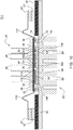
- the electronic assembly 211 of FIG. 4 is similar to the electronic assembly 111 of FIG. 2 , except the electronic assembly 211 further comprises a supplemental substrate 56 or circuit board that intervenes between the second substrate or second heat sink 24 and the semiconductor device 14.
- the supplemental substrate 56 comprises a single-sided or double-sided circuit board that has an upper surface 58 with conductive mating surfaces 62 and conductive traces 64 for interfacing with one or more of the following on the semiconductor device 14: (1) primary metallic surface 22, (2) secondary metallic surface 23, or both.
- a dielectric region 66 separates the conductive mating surfaces 62 into two separate regions that may be associated with corresponding conductive traces 64.
- Each of the separate regions or conductive traces 64 may be associated with different terminals of the semiconductor device 14, such as a collector terminal of a transistor and a cathode terminal a protective diode associated with the transistor.
- the dielectric region 45 is aligned or registered with the dielectric region 66 to maintain electrical isolation and to support discrete separate terminals for the primary metallic surface 22 and the secondary metallic surface 23.
- the conductive traces 64 may terminate in conductive pads for connection to the circuit board 25, or conductive traces 64 on the circuit board 25 via solder joints 67 or other electrical connections.
- a lower surface 60 of the supplemental substrate 56 comprises a dielectric layer 65 that adjoins or contacts a second base 30 of the second heat sink 24.
- the dielectric layer 65 may have an optional thermal grease or thermally conductive adhesive between the dielectric layer 65 and the second base 30 of the second heat sink 24 to facilitate heat transfer of thermal energy away from the semiconductor device 14.
- a lower surface 60 of the supplemental substrate 56 comprises a conductive ground plane (e.g., metallized outer layer) and the supplemental substrate 56 comprises a double-sided circuit board, where the conductive ground plane can be connected to or bonded to the second heat sink 24 via a third bonding layer of solder, or a combination of solder and copper material.
- a conductive ground plane e.g., metallized outer layer
- the supplemental substrate 56 comprises a double-sided circuit board, where the conductive ground plane can be connected to or bonded to the second heat sink 24 via a third bonding layer of solder, or a combination of solder and copper material.
- conductive vias or plated through holes can connect the at least one mating pad to the ground plane.
- FIG. 5 is a plan view of a plurality of illustrative lead frames 110 suitable for any of the electronic assemblies (e.g., 11, 111, 211, 311).
- the first substrate may comprise one or more lead frames 110.
- the first substrate comprises a lead frame 110 having a substantially planar portion 46 with a series or grid of holes 54 for interfacing with the first bonding layer 12 (e.g., solder).
- the first bonding layer 12 e.g., solder
- the substantially planar portion 46 of the lead frame 110 is centrally disposed for mating in registration or alignment with one or more of the following via the first bonding layer 12: (1) a corresponding first conductive pad 34, (2) a corresponding second conductive pad 38, and (3) a corresponding third conductive pad 40 of the semiconductor device 14. Further, in some embodiments, the substantially planar portion 46 of the lead frame 110 is divided or subdivided into discrete sections that are not electrically and mechanically connected, but separated by air gap or dielectric gaps to allow for multiple separate semiconductor terminals to be supported simultaneously, such as a gate terminal or base terminal, an emitter terminal or source terminal, a collector terminal or source terminal, and an anode terminal or cathode terminal.
- solder outgassing holes 54 in the planar portion 46 of the lead-frames 110 can be connected to one or more semiconductor devices 14 (e.g., semiconductor dies), such as insulated gate bipolar junction transistor (IGBT) dies, diode dies, or both.
- semiconductor dies such as insulated gate bipolar junction transistor (IGBT) dies, diode dies, or both.
- IGBT insulated gate bipolar junction transistor
- diode dies diode dies
- Each semiconductor die may be mounted or manufactured as a direct-bonded-copper substrate.
- the holes 54 serve as solder outgassing outlets and also allows for the creation of an array of solder fillets on the surface of lead-frames 110 at the end of soldering.
- Outgassing of liquid solder supports reduced opportunity for void formation in solidified bond-layer of the first bonding layer 12.
- reduced voiding and the presence of solder fillet on the top surface of lead-frame 110 can enhance the thermomechanical reliability of first bonding layer 12; hence, the assembly (11, 111, 211, or 311) or power module while in operation.
- Each lead frame 110 terminates in terminals (48, 50) or fingers 52 that can be connected to other circuitry of an electronic assembly (11, 11, 211, 311) via conductors, conductive traces of circuit board 25, wire, cables, or transmission line.
- the terminal 48 of the lead frame 110 with the largest surface area or mass may be assigned to the collector or drain of a semiconductor device 14; the terminal 50 of the lead frame 110 with the second largest surface area or mass may be assigned to the emitter or source of the semiconductor device 14, although other assignments of terminals are possible and fall within the scope of the claims.
- the terminal 48 of lead frame with the largest surface area or mass may be assigned to the emitter or source of the semiconductor device 14; the terminal 50 of the lead frame 110 with the second largest surface area or mass may be assigned to the collector or drain of the semiconductor device 14.
- FIG. 6 is one embodiment of flow chart for a method for making an electronic assembly (11, 111 211, or 311) with enhanced thermal dissipation. The method of FIG. 6 begins in step S500.
- solder paste is deposited onto a second substrate 18, such as a second base 30 of a second heat sink 24 or a circuit board (e.g., double-sided circuit board with ground plane and one or more conductive vias) engineered for thermal dissipation.
- a dispenser or applicator dispenses or applies solder paste onto or to the second substrate 18.
- step S502 copper material is embedded or provided in the deposited solder paste.
- Step S502 may be executed before, after or during step S500.
- copper material is added to the solder paste during or after the depositing of the solder paste.
- copper pellets are added to the solder paste after the solder paste is deposited onto the second substrate 18 in step S500.
- the embedding or providing of the copper material can lower a homologous temperature of the second bonding layer (16 or 116) to facilitate greater mechanical strength of a bond between the second bonding layer (16 or 116) and the primary metallic surface 22, and/or a bond between the second bonding layer 16 and the secondary metallic surface 23.
- a dispenser or applicator deposits solder paste (e.g., in a matrix pattern) on a plurality of upper conductive pads (34, 38, 40) of one or more semiconductor devices 14.
- the dispenser or applicator deposits solder paste onto the first conductive pad 34, the second conductive pads 38 and a third conductive pad 40.
- each semiconductor device 14 has a first side 42 or upper side with the first conductive pad 34, the second conductive pad 38 and the third conductive pad; each semiconductor device 14 has a second side 44 opposite the first side 42.
- one or more semiconductor devices 14 are placed and aligned on the second substrate 18 or second heat sink 24.
- a pick-and-place machine places and aligns the one or more semiconductor devices 14 (e.g., semiconductor dies) on the second substrate 18 or on a substantially planar surface of second base 30 of the second heat sink 24.
- a first substrate 10 or one or more lead frames 110 are placed and aligned on one or more of the following: a corresponding first conductive pad 34, a corresponding second conductive pad 38 and a corresponding third conductive pad 40.
- a pick-and-place machine places and aligns the first substrate or lead frame 110 on the corresponding first conductive pad 34 of each semiconductor device 14 to assign or allocate to the first conductive pad 34 to a first terminal of the lead frame 110, to assign or allocate to the second conductive pad 38 a second terminal of the lead frame 110, and to assign or allocate to the third conductive pad 40 a third terminal of the lead frame 110.
- the semiconductor manufacturer or designer assigns the each conductive pad (34, 38, 40) a particular input/output port or node of the semiconductor device 14, such as a gate, source or drain terminal.
- step S510 the assembly (11, 111, 211, 311) is heated once in a single thermal cycle (e.g., only one-time in a reflow oven) to form a first bonding layer, 12 or 112, 212 and 312, (e.g., first metallic bonding layer) between the first substrate (e.g., lead frame 110) and the upper conductive pads (34, 38, 40) and to form a second bonding layer 16 or 116 (e.g., second metallic bonding layer) between the second substrate 18 (e.g., second heat sink 24) and one or more metallic surfaces (22, 23 or both), such as one or more lower conductive pads.
- a first bonding layer 12 or 112, 212 and 312, (e.g., first metallic bonding layer) between the first substrate (e.g., lead frame 110) and the upper conductive pads (34, 38, 40) and to form a second bonding layer 16 or 116 (e.g., second metallic bonding layer) between the second substrate 18 (e.g
- Step S510 may be carried out in accordance with various techniques that may be applied separately or cumulatively.
- the assembly (11, 111, 211, 311) is heated once in a single thermal cycle (e.g., only one-time in a reflow oven) to form a first bonding layer, 12 or 112, 212 and 312, between one or more lead frames 110 and the upper conductive pads (34, 38, 40) on the first side 42 and to form a second bonding layer 16 or 116 between the second heat sink 24 and a primary metallic surface 22 (or both primary metallic surfaces 22 and secondary metallic surface 23) on the second side 44 of the one or more semiconductor devices 14.
- a first technique the assembly (11, 111, 211, 311) is heated once in a single thermal cycle (e.g., only one-time in a reflow oven) to form a first bonding layer, 12 or 112, 212 and 312, between one or more lead frames 110 and the upper conductive pads (34, 38, 40) on the first side 42 and to form a second
- an oven heats the assembly (11, 111, 211, 311) in a soldering chamber in accordance with a thermal reflow process to form a first bonding layer 12 (e.g., first metallic bonding layer) between the first substrate 10 (e.g., lead frames 110) and the conductive pads (34, 38, 40) and to form a second bonding layer (e.g., second metallic bonding layer) between the second substrate 18 and primary metallic surfaces 22 on the second side 44 of the one or more semiconductor devices 14.
- a first bonding layer 12 e.g., first metallic bonding layer
- first substrate 10 e.g., lead frames 110
- the conductive pads 34, 38, 40
- Heating the assembly (11, 111, 211) once occurs in a single heating cycle. Heating the assembly (11, 111, 211) once is well-suited for reducing a layer thickness of a solder layer intermetallic compound (in the bonding layers 12, 16) to facilitate integrity of the first bonding layer 12 and the second bonding layer 16.
- the first bonding layer 12 and the second bonding layer 16 comprise two intermetallic compound (IMC) bond-layers that are simultaneously formed through melting, wetting and spreading of the solder paste material during soldering.
- the IMC layers binds or bonds both the first side 42 of the semiconductor devices 14 to the lead-frames 110 and second side 44 to a heatsink (e.g., second heat sink 24) or heat-sinking circuit board.
- FIG. 9 shows a plan view of a fully built and functional electronic assembly (11, 111, 211) or sub-assembly for an inverter or other power electronics module.
- the first bonding layer 12 and the second bonding layer 16 are formed simultaneously during a single heating cycle or reflow process where the melting temperature range of the solder material, such as lead-free solder material should be approximately 217 degrees Celsius to approximately 230 Celsius.
- the first bonding layer 12 and the second bonding layer 16 are formed simultaneously during a single heating cycle or reflow process where the melting temperature range of the solder material, such as leaded solder paste (where lawful and applicable) is approximately 180 degrees Celsius to approximately 190 degrees Celsius.
- the melting temperature range of the solder material such as leaded solder paste (where lawful and applicable) is approximately 180 degrees Celsius to approximately 190 degrees Celsius.
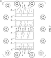
- FIG. 7 is a plan view of a second substrate 18, such as a substantially planar surface of a second base 30 of a second heat sink 24 with solder paste, with or without copper material, arranged in generally rectangular matrices 116 on conductive members for mating with a respective primary metallic surface 22, secondary metallic surface 23, or both on one or more semiconductor devices 14.
- FIG. 7 illustrates the result or completion of step S500 of FIG. 6 .
- FIG. 8 is a plan view of a plurality of semiconductor devices 14 with solder paste arranged in matrices on their respective conductive pads, such as the first conductive pad 34, the second conductive pad 38 and third conductive pad 40.
- the conductive pads (34, 38, 40) are illustrated as generally rectangular regions that underlie a corresponding matrix of solder paste or a combination of solder paste and copper material.
- the first matrix 112 of solder paste or combined solder paste and copper material overlies the corresponding first conductive pad 34, which is composed of copper or a copper alloy; the second matrix 212 of solder paste or combined solder paste and copper material overlies the corresponding second conductive pad 38, which is composed of copper or a copper alloy; the third matrix 312 of solder paste or combined solder paste and copper material overlies the corresponding third conductive pad 40, which is composed of copper or a copper alloy.
- FIG. 8 illustrates the result or completion of step S504 of FIG. 6 .
- FIG. 9 is a plan view of one embodiment of an electronic assembly (11, 111 or 211).
- FIG. 9 illustrates the result or completion of step S506, step S508, or both of FIG. 6 .
- each bond-layer such as the first bonding layer 12 and the second bonding layer 16
- the disclosed method and the associated structure reduces the heating or manufacturing cycles from two to one cycle, which can be referred to as single pass heating process or single pass reflow process.
- the single pass heating process can reduce manufacturing cost, manufacturing time, and manufacturing thermal energy input, or can increase manufacturing throughput volume of manufactured units.
- FIG. 10 is an alternate embodiment of a cross-section of an electronic assembly 311 as viewed along reference line 10-10 of FIG. 11A .
- the electronic assembly 311 of FIG. 10 is similar to the electronic assembly 111 of FIG. 2 , except that a second side 44 of the semiconductor device 14 comprises a primary metallic surface 122 that occupies a majority of the surface area of the second side 44 to form a metallic ground plane.
- the second side 44 of each semiconductor device 14 has no dielectric region 45 and the second metallic surface 23 is omitted.
- the second bonding layer 16 or 116 is formed between the primary metallic surface 122 and a substantially planar surface of the second base 30 of the second heat sink 24.
- the second bonding layer 16 may be composed of solder or a combination of solder and copper material.
- FIG. 11A is a plan view of a first side (e.g., upper side) of one illustrative embodiment of a semiconductor device in accordance with FIG. 10 .
- Like reference numbers in FIGS. 10 , 11A and 11B indicate like elements or features.
- FIG. 11B is a plan view of a second side (e.g., lower side) of one illustrative embodiment of the semiconductor device, consistent with FIG. 10 and FIG. 11A .
- the method disclosed herein is well suited for manufacturing with lead-free solder materials, silicon semiconductors, or silicon carbide semiconductors. Solder materials may be required to comply with environmental regulations and directives, such as Directive 2011/65/EU of the European Parliament and of the council of 8 June 2011.
- the method of electronic assembly (11, 11 or 211) facilitate cost-effective and reliable operation of the electronics assembly (11, 11 or 211) under harsh conditions such as high temperatures, high voltages and currents, high shock and vibration, and varying application environments.
- the method disclosed herein is also well-suited for enhanced double-sided heat dissipation that meet or exceed high temperature applications, such as those at or above 200 degrees Celsius.
Landscapes
- Cooling Or The Like Of Semiconductors Or Solid State Devices (AREA)
- Engineering & Computer Science (AREA)
- Manufacturing & Machinery (AREA)
- Chemical & Material Sciences (AREA)
- Ceramic Engineering (AREA)
Abstract


Description
- This disclosure relates to an electronic assembly with enhanced thermal dissipation.
- Certain prior art uses bonded wire to connect the leads of a semiconductor device to a semiconductor package or substrate. However, the thermal dissipation, the operational temperature range, or the maximum operating temperature of the semiconductor device may be limited because of the bonded wire connections. Some semiconductor devices may use silicon carbide for its superior power handling capabilities. However, silicon carbide presents challenges in semiconductor packaging with respect to providing adequate thermal dissipation. Thus, there is a need for an electronic assembly with enhanced thermal dissipation.
- In accordance with one aspect of the disclosure, an electronic assembly comprises a semiconductor device with a first side and a second side opposite the first side. The first side has a first conductive pad. The second side has a primary metallic surface. A first substrate (e.g. lead frame) is bonded to the first conductive pad via first metallic bonding layer. A second substrate (e.g., heat sinking circuit board) is bonded to the at least primary metallic surface via a second metallic bonding layer. In one configuration the second metallic bonding layer is composed of solder and copper, for example.
-
-
FIG. 1 is one embodiment of a block diagram that is representative of a cross-section of an electronic assembly of the disclosure. -
FIG. 2 is another embodiment of a cross-section of an electronic assembly as viewed along reference line 2-2 ofFIG. 3A . -
FIG. 3A is a plan view of a first side (e.g., upper side) of one illustrative embodiment of a semiconductor device in accordance withFIG. 2 . -
FIG. 3B is a plan view of a second side (e.g., lower side) of one illustrative embodiment of the semiconductor device, consistent withFIG. 2 andFIG. 3A . -
FIG. 4 is a cross-section of an alternate embodiment of an electronic assembly that features an additional substrate (e.g., circuit board) between a semiconductor device and a heat sink. -
FIG. 5 is a plan view of a plurality of illustrative lead frames suitable for the electronic assembly. -
FIG. 6 is one embodiment of flow chart for a method for making an assembly with enhanced thermal dissipation. -
FIG. 7 is a plan view of a second substrate, such as a heat sink with solder paste on conductive members for mating with respective conductive pads on one or more semiconductor devices. -
FIG. 8 is a plan view of a plurality of semiconductor devices with solder paste on their respective conductive pads. -
FIG. 9 is a plan view of one embodiment of a fully assembled electronic assembly. -
FIG. 10 is an alternate embodiment of a cross-section of an electronic assembly as viewed along reference line 10-10 ofFIG. 11A . -
FIG. 11A is a plan view of a first side (e.g., upper side) of one illustrative embodiment of a semiconductor device in accordance withFIG. 10 . -
FIG. 11B is a plan view of a second side (e.g., lower side) of one illustrative embodiment of the semiconductor device, consistent withFIG. 10 andFIG. 11A . - In any group of the drawings, like reference numbers indicate like elements, features, processes or steps.
-
FIG. 1 is a block diagram that is representative of a cross-section of one embodiment of anelectronic assembly 11 of the disclosure. In accordance withFIG. 1 , anelectronic assembly 11 comprises asemiconductor device 14 with afirst side 42 and asecond side 44 opposite thefirst side 42. Thefirst side 42 has a firstconductive pad 34. Thesecond side 44 has a primarymetallic surface 22. A first substrate 10 (e.g. lead frame) is bonded to the firstconductive pad 34 via firstmetallic bonding layer 12. A second substrate 18 (e.g., heat sink or heat-sinking circuit board) is bonded to the primarymetallic surface 22 via a secondmetallic bonding layer 16. - The
first bonding layer 12 provides an electrical and mechanical connection between the firstconductive pad 34 and the first substrate 10 (e.g., one or more lead frames). Alternatively, thefirst bonding layer 12 provides a set of respective electrical and mechanical connections to different terminals of a lead frame for a corresponding firstconductive pad 34, a corresponding secondconductive pad 38 and corresponding thirdconductive pad 40. - The
second bonding layer 16 provides an electrical and mechanical connection between the primarymetallic surface 22 and the second substrate 18 (e.g., heat sink or heat-sinking circuit board). Alternatively, thesecond bonding layer 16 provides an electrical and mechanical connection between the primarymetallic surface 22, the secondarymetallic surface 23 and the second substrate (e.g. heat sink or heat sinking circuit board). - In one embodiment, the
first bonding layer 12 is composed of solder; thesecond bonding layer 16 is composed of solder or both solder and copper material. However, in an alternate embodiment, thefirst bonding layer 12 is composed of both solder and copper material. - In the
first bonding layer 12, thesecond bonding layer 16, or both, the copper content (e.g., copper pellets) can facilitate enhanced heat dissipation from thesemiconductor device 14. Further, the copper content can promote improved thermomechanical strength of one or more bonding layers (12, 16). For example, in one embodiment, the copper (in the first bonding layer 12) lowers a homologous temperature of thefirst bonding layer 12 to facilitate greater mechanical strength (e.g., sheer, tensile and/or compressive strength) of a bond between thefirst bonding layer 12 and the firstconductive pad 34. Similarly, in one embodiment, the copper (in the second bonding layer 16) lowers a homologous temperature of thesecond bonding layer 16 to facilitate greater mechanical strength (e.g., sheer, tensile and/or compressive strength) of a bond between thesecond bonding layer 16 and the primarymetallic surface 22. - In one configuration, the
semiconductor device 14 has a primary coefficient of thermal expansion (CTE), whereas the first substrate 10 (e.g., lead frame) or secondary substrate 18 (e.g., heatsink) has a secondary coefficient of thermal expansion (CTE), and wherein the copper in thefirst bonding layer 12 or thesecond bonding layer 16, respectively, reduces a mismatch (and associated thermal stress) between the primary CTE and the secondary CTE. - In an alternate embodiment, the
semiconductor device 14 further comprises a secondconductive pad 38 and a thirdconductive pad 40 on thefirst side 42. As shown inFIG. 1 , thesecond pad 38 and the thirdconductive pad 40 are optional as indicated by the dashed lines. Similarly, in an alternate embodiment, thesemiconductor device 14 further comprises a secondarymetallic surface 23, which is optional as indicated by the dashed lines inFIG. 1 . - Any or all of the conductive pads (34, 38, 40) are composed of electrically conductive materials, such as metal (e.g., copper), alloys or metallic materials.
-
FIG. 2 is an embodiment of a cross-section of anelectronic assembly 111 taken along reference line 2-2 ofFIG. 3A and FIG. 3B .FIG. 2 shows an illustrative example of one possible cross-section of anelectronic assembly 111. Like reference numbers in any permutation ofFIG. 1 ,FIG. 2 ,FIG. 3A and FIG. 3B indicate like elements or features. - In one embodiment, the first substrate comprises one or more
lead frames 110 for interfacing with at least the firstconductive pad 34 on arespective semiconductor device 14. In another embodiment, the first substrate comprises a plurality oflead frames 110 for interfacing with the corresponding firstconductive pads 34 on a corresponding plurality ofrespective semiconductor devices 14. As illustrated inFIG. 2 , eachlead frame 110 engages, interfaces or registers with the correspondingconductive pad 34, the corresponding secondconductive pad 38 and corresponding thirdconductive pad 40 associated with thefirst side 42 of thesemiconductor device 14, such as semiconductor die. - In one embodiment, as best illustrated in
FIG. 2 andFIG. 3A , the firstconductive pad 34 may comprise a continuous metallic member (e.g., with a rectangular or polygonal surface area), where afirst matrix 112 of solder paste is placed on a grid, array or pattern of islands on the firstconductive pad 34; the secondconductive pad 38 may comprise a continuous metallic member (e.g., with a rectangular or polygonal surface area), where asecond matrix 212 of solder paste is placed on a grid, array or pattern of islands on the secondconductive pad 38; the thirdconductive pad 40 may comprise a continuous metallic member (e.g., with a rectangular or polygonal surface area), where athird matrix 312 of solder paste is placed on a grid, array or pattern of islands on the thirdconductive pad 40. The solder paste is reflowed during the manufacturing of theassembly 111, for example. Collectively, thefirst matrix 112 of solder paste, thesecond matrix 212 of solder paste and thethird matrix 312 of solder paste may be referred to as thefirst bonding layer 12. - In an alternate embodiment, a set of first conductive pads comprise a grid or array of conductive metallic islands that are spaced apart by a lateral gap (e.g., lateral dielectric gap or air gap) on the
first side 42 of thesemiconductor device 14. Similarly, a set of second conductive pads comprise a grid or array of conductive metallic islands that are spaced apart by a lateral gap (e.g., lateral dielectric gap or air gap) on thefirst side 42 of thesemiconductor device 14; a set of third conductive pads comprise a grid or array of conductive metallic islands that are spaced apart by a lateral gap (e.g., lateral dielectric gap or air gap) on thefirst side 42 of thesemiconductor device 14. In the alternate embodiment, the first, second and third matrices (112, 212, 312) of solder paste are spatially aligned with, and coextensive in size and shape with, the underlying set of first conductive pads, the underlying set of second conductive pads and the underlying set of third conductive pads. - In one configuration, each
lead frame 110 has a substantiallyplanar portion 46 that has a lower surface for interfacing with the firstconductive pad 34 on thesemiconductor device 14 and an upper surface for coupling or receiving, directly or indirectly, afirst heat sink 20. Further, the substantiallyplanar portion 46 may interface with the firstconductive pad 34, the secondconductive pad 38 and the thirdconductive pad 40. For example, eachfirst bonding layer 12 may interconnect one or more lead frames 110 (via its lower surface) to the corresponding firstconductive pad 34, the corresponding secondconductive pad 38 and the corresponding thirdconductive pad 40 of one or morerespective semiconductor devices 14. Further, the firstconductive pad 34 is associated with a corresponding first terminal of thesemiconductor device 14, the secondconductive pad 38 is associated with a corresponding second terminal of thesemiconductor device 14 and the thirdconductive pad 40 is associated with a third terminal of thesemiconductor device 14, where each terminal represents a distinct node or port (e.g., input or output port) of thesemiconductor device 14. Although other configurations of the terminals are possible, in one configuration the first terminal comprises an anode of a diode, wherein the second terminal comprises an emitter or source of a transistor and the third terminal comprises a base or a gate of the transistor. - The
first bonding layer 12 may comprise a continuous metallic layer (e.g., after reflow of the solder or solder and copper) or may comprise afirst matrix 112, asecond matrix 212, and a third matrix 312 (e.g., grid or array in one or two dimensions) of discontinuous conductive islands that are spaced apart by at least one lateral air gap or lateral isolation gap to support different leads or terminals for eachsemiconductor device 14. In one configuration, the first terminal or firstconductive pad 34 is associated with the respectivefirst matrix 112, the second terminal or secondconductive pad 38 is associated with the respectivesecond matrix 212, and the third terminal or thirdconductive pad 40 is associated with thethird matrix 312. - As illustrated, a thermal interface layer 36 (e.g., dielectric thermal interface material) or other dielectric layer is disposed between the lead frame 110 (or its upper surface) and the
first heat sink 20, or itsfirst base 32. In one configuration, thefirst heat sink 20 has a substantially planar mating surface orfirst base 32 for adjoining thethermal interface material 36.Fins 26, ridges or other protrusions extend outward from a side of thefirst heat sink 20 that is opposite the substantially planar mating surface. - In one embodiment, the first substrate comprises a
lead frame 110 having a substantiallyplanar portion 46 with a series or grid of holes 54 (inFIG. 5 ) for interfacing with the first bonding layer 12 (e.g., first metallic bonding layer). For example, the first substrate comprises alead frame 110 that is capable of laterally spreading or dissipating heat to reduce any temperature differential within different portions of theelectronic assembly 111, or among a plurality ofsemiconductor devices 14 of theelectronic assembly 111. - As illustrated in
FIG. 2 , the second substrate comprises asecond heat sink 24 with asecond base 30. Thesecond base 30 has a substantially planar surface for interconnection with the primarymetallic surface 22, the secondarymetallic surface 23, or both, of the one ormore semiconductor devices 14. Thesecond bonding layer 16 facilitates the interconnection between thesecond base 30 orsecond heat sink 24 and the primarymetallic surface 22, the secondarymetallic surface 23 or both of the one ormore semiconductor devices 14.Fins 28, ridges or other protrusions extend outward from a side of thesecond heat sink 24 that is opposite the substantially planar surface. - In one embodiment, the
first bonding layer 12 may comprise one or more of the following matrices of solder paste or a combination of solder paste and copper material: afirst matrix 112, asecond matrix 212 or athird matrix 312. In one embodiment, thefirst bonding layer 12 or first metallic bonding layer is composed of solder material, such as a composition of tin and silver, lead solder, or another suitable lead-free solder material. In an alternate embodiment, thefirst bonding layer 12 may comprise a combination of solder and copper material. For example, thefirst bonding layer 12 comprises solder material (e.g., a lead-free solder material) and copper pellets coated with a solderable finish such as tin, silver or electroless nickel immersion gold (ENIG). - In one embodiment, the solder material or solder paste is a lead-free solder material or alloy composition, such as tin-silver, tin-silver-copper, or tin-gold, or tin and one or more other metallic elements, such as antimony, bismuth, indium, or zinc. For example, tin-silver-copper solder alloy composition can be composed of approximately 2.5 to 4 percent silver by mass, approximately .25 to 1 percent copper by mass with the remaining mass being tin or a composition of tin. For solder paste, the solder powder size range should be: 20-38 microns and the solder paste is 90 percent metal load (percentage-by-weight of solder in the paste).
- In alternate embodiments, solder paste can contain lead, such as tin-silver-lead or tin-lead, if the lead-containing solder material is authorized under applicable law and regulations, such as military specifications.
In one embodiment, copper material or additional copper material is added to the above solder material or alloy composition, such that the copper content may exceed the range of .25 to 1 percent copper by mass of thefirst bonding layer 12 of thesecond bonding layer 16. For example, embedded copper material in the solder paste can be in the form of discs plated with a solderable finish such as tin, silver, or ENIG, among other possibilities. In one illustrative configuration, the diameter and thickness of the disc is 0.025 inches (0. 625mm) with a tolerance of ±0.002 inches and 0.010 inches (0.25mm) with a tolerance of ±0.001 inches respectively and the percentage volume in the solder paste/copper composite ranges from approximately 15 percent to approximately 40 percent. In one embodiment, thesecond bonding layer 16 may comprise one or more separate islands, bodies, or matrices (e.g., 116 inFIG. 7 ) of solder paste or a composition (e.g., alloy composition) of solder (e.g., lead-free solder, even including up to 1 percent copper by mass) and copper material (e.g., copper particles, copper flakes, copper pellets, or copper filler). In one configuration, thesecond bonding layer 16 or second metallic bonding layer is composed of copper material and solder material, such as a composition of tin and silver, lead solder, or another suitable lead-free solder material. In one embodiment, the copper comprises copper pellets coated with tin, silver, or electroless nickel immersion gold. The copper is well-suited to lower a homologous temperature of thesecond bonding layer 16 to facilitate greater mechanical strength of a bond between thesecond bonding layer 16 and the primary metallic surfaces 22. - In one configuration, the
semiconductor device 14 is capable of generating heat, thefirst bonding layer 12 and thesecond bonding layer 16 comprise metallic materials or thermal interface materials that conduct simultaneously the heat away from one ormore semiconductor devices 14 from eachfirst side 42 of eachsemiconductor device 14 and from eachsecond side 44 of each semiconductor device 14 (among the devices). - In certain configurations, the
semiconductor device 14 has a primary coefficient of thermal expansion (CTE) and the first substrate 10 (e.g., lead frames 110) or the second substrate 18 (e.g., second heat sink 24) has a secondary coefficient of thermal expansion (CTE); the copper in thefirst bonding layer 12 or thesecond bonding layer 16, respectively, reduces a mismatch (and associated thermal stress) between the primary CTE and the secondary CTE. - In one embodiment, the
electronic assembly 111 comprises a set ofsemiconductor devices 14. For example, eachsemiconductor device 14 comprises a semiconductor die, such as an insulated gate bipolar transistor (IGBT) or an insulated gate bipolar transistor and a diode on or in a direct bonded copper carrier or semiconductor substrate. Eachsemiconductor device 14 is capable of generating heat during normal operation. Thefirst bonding layer 12 and thesecond bonding layer 16 comprise thermal interface materials that conduct simultaneously the heat away from thesemiconductor device 14 from afirst side 42 of thesemiconductor device 14 and from asecond side 44 of thesemiconductor device 14. The first substrate comprises one or morelead frames 110 that are capable of laterally spreading or dissipating the heat to reduce any temperature differential within different portions of theelectronic assembly 111, or among a plurality ofsemiconductor devices 14 of theelectronic assembly 111. - In one embodiment, the first substrate comprises a
lead frame 110 with a substantiallyplanar portion 46 having a lower surface for interfacing with the corresponding firstconductive pad 34, secondconductive pad 38, and thirdconductive pad 40 on thesemiconductor device 14. Further, the substantiallyplanar portion 46 of thelead frame 110 has an upper surface for coupling or receiving, directly or indirectly, afirst heat sink 20. For example, the upper surface of the substantially planar portion 46 (of the lead frame 110) adjoins the dielectric thermal interface material 36 (e.g., thermally conductive adhesive), which is sandwiched between the upper surface and thefirst heat sink 20 or itsfirst base 32. Thelead frame 110 terminates in afirst terminal 48 and asecond terminal 50, which can be connected toconductive traces 57 on thecircuit board 25 via solder joints 67. As illustrated inFIG. 2 , thecircuit board 25 has anopening 59 of a size and shape to receive thesemiconductor device 14 with a peripheral clearance gap. Thecircuit board 25 may be composed of a ceramic, polymeric, plastic, polymer with glass filler, for example, with conductive traces on one or both sides. -
FIG. 3A is a plan view of a first side 42 (e.g., upper side) of one illustrative embodiment of asemiconductor device 14. Thefirst side 42 of thesemiconductor device 14 comprises the firstconductive pad 34, the secondconductive pad 38 and the thirdconductive pad 40 which are laterally separated from each other by one or moredielectric barriers 145. Eachdielectric barrier 145 represents an air gap, a ceramic insulating region, a plastic or polymer insulating region, or another dielectric region. In one embodiment, each firstconductive pad 34, each secondconductive pad 38 and each thirdconductive pad 40 is associated with a corresponding lead or terminal of arespective semiconductor device 14. For example, any pad (34, 38 and 40) may represent: (1) a gate pad or base pad, (2) an emitter pad or source pad, (3) an anode pad, or (4) a cathode pad. - An enlarged surface area for a corresponding pad (34, 38, 40) or set of pads of a
semiconductor device 14 facilitates enhanced heat dissipation for asemiconductor device 14. As illustrated, the firstconductive pad 34, the secondconductive pad 38 and the thirdconductive pad 40 are arranged as a grid or an array of substantially rectangular metallic pads that are separated bydielectric barriers 145, dielectric intermediate regions or dielectric borders, where the pads (34, 38, 40) occupy collectively a majority of thefirst side 42 of thesemiconductor device 14.FIG. 8 illustrates a plane view of foursemiconductor devices 14 with thefirst matrix 112, thesecond matrix 212 and thethird matrix 312 of solder paste deposited on one or more of the following: the at least one firstconductive pad 34, the at least one secondconductive pad 38 and the at least one thirdconductive pad 40. -
FIG. 3B is a plan view of a second side 44 (e.g., lower side) of one illustrative embodiment of thesemiconductor device 14, consistent withFIG. 3A . In one embodiment, thesecond side 44 of thesemiconductor device 14 comprises a primarymetallic surface 22, a secondarymetallic surface 23, or both. For example, the primarymetallic surface 22 may comprise one or more of the following metallic or conductive pads: (1) a gate pad or base pad, (2) a collector pad or drain pad, and (3) a cathode pad, and (4) an anode pad. In one configuration, metallic surfaces (22, 23) with an enlarged surface area for a corresponding terminal of asemiconductor device 14 facilitate enhanced heat dissipation compared to a minimal surface area required to carry the target (e.g., designed or peak load) electrical current from the corresponding terminal of asemiconductor device 14. As illustrated, the primarymetallic surface 22 and the secondarymetallic surface 23 are arranged as a grid or an array of substantially rectangular metallic pads that are separated by adielectric region 45, or dielectric borders. Thedielectric region 45 represents an intermediate or intervening dielectric barrier between the primarymetallic surface 22 and the secondarymetallic surface 23. For example, thedielectric region 45 may be defined by an air gap, a ceramic insulating region, a polymeric or plastic insulating region, or another insulating region, where a ceramic or polymeric region that is flush with the primarymetallic surface 22 and the secondarymetallic surface 23 inhibits the flow of solder (e.g., of the second bonding layer 16) into any gap between the pads that might otherwise form a short circuit or unwanted capacitive coupling. Here, the primarymetallic surface 22 and the secondarymetallic surface 23 occupy, collectively, a majority of the surface area of thesecond side 44 of thesemiconductor device 14. - The
electronic assembly 211 ofFIG. 4 is similar to theelectronic assembly 111 ofFIG. 2 , except theelectronic assembly 211 further comprises asupplemental substrate 56 or circuit board that intervenes between the second substrate orsecond heat sink 24 and thesemiconductor device 14. - As illustrated in
FIG. 4 , thesupplemental substrate 56 comprises a single-sided or double-sided circuit board that has an upper surface 58 with conductive mating surfaces 62 andconductive traces 64 for interfacing with one or more of the following on the semiconductor device 14: (1) primarymetallic surface 22, (2) secondarymetallic surface 23, or both. As illustrated, adielectric region 66 separates the conductive mating surfaces 62 into two separate regions that may be associated with corresponding conductive traces 64. Each of the separate regions orconductive traces 64 may be associated with different terminals of thesemiconductor device 14, such as a collector terminal of a transistor and a cathode terminal a protective diode associated with the transistor. As shown, thedielectric region 45 is aligned or registered with thedielectric region 66 to maintain electrical isolation and to support discrete separate terminals for the primarymetallic surface 22 and the secondarymetallic surface 23. Further, the conductive traces 64 may terminate in conductive pads for connection to thecircuit board 25, orconductive traces 64 on thecircuit board 25 viasolder joints 67 or other electrical connections. - As illustrated, a
lower surface 60 of thesupplemental substrate 56 comprises adielectric layer 65 that adjoins or contacts asecond base 30 of thesecond heat sink 24. Thedielectric layer 65 may have an optional thermal grease or thermally conductive adhesive between thedielectric layer 65 and thesecond base 30 of thesecond heat sink 24 to facilitate heat transfer of thermal energy away from thesemiconductor device 14. - In an alternate embodiment, a
lower surface 60 of thesupplemental substrate 56 comprises a conductive ground plane (e.g., metallized outer layer) and thesupplemental substrate 56 comprises a double-sided circuit board, where the conductive ground plane can be connected to or bonded to thesecond heat sink 24 via a third bonding layer of solder, or a combination of solder and copper material. - In another alternate embodiment where the
supplemental substrate 56 comprises a double-sided circuit board, conductive vias or plated through holes can connect the at least one mating pad to the ground plane. -
FIG. 5 is a plan view of a plurality of illustrative lead frames 110 suitable for any of the electronic assemblies (e.g., 11, 111, 211, 311). The first substrate may comprise one or more lead frames 110. In one embodiment, the first substrate comprises alead frame 110 having a substantiallyplanar portion 46 with a series or grid ofholes 54 for interfacing with the first bonding layer 12 (e.g., solder). As illustrated inFIG. 5 andFIG. 9 , the substantiallyplanar portion 46 of thelead frame 110 is centrally disposed for mating in registration or alignment with one or more of the following via the first bonding layer 12: (1) a corresponding firstconductive pad 34, (2) a corresponding secondconductive pad 38, and (3) a corresponding thirdconductive pad 40 of thesemiconductor device 14. Further, in some embodiments, the substantiallyplanar portion 46 of thelead frame 110 is divided or subdivided into discrete sections that are not electrically and mechanically connected, but separated by air gap or dielectric gaps to allow for multiple separate semiconductor terminals to be supported simultaneously, such as a gate terminal or base terminal, an emitter terminal or source terminal, a collector terminal or source terminal, and an anode terminal or cathode terminal. - In one embodiment, the solder outgassing holes 54 in the
planar portion 46 of the lead-frames 110 can be connected to one or more semiconductor devices 14 (e.g., semiconductor dies), such as insulated gate bipolar junction transistor (IGBT) dies, diode dies, or both. Each semiconductor die may be mounted or manufactured as a direct-bonded-copper substrate. - As shown in
FIG. 5 , theholes 54 serve as solder outgassing outlets and also allows for the creation of an array of solder fillets on the surface of lead-frames 110 at the end of soldering. Outgassing of liquid solder supports reduced opportunity for void formation in solidified bond-layer of thefirst bonding layer 12. For example, reduced voiding and the presence of solder fillet on the top surface of lead-frame 110 can enhance the thermomechanical reliability offirst bonding layer 12; hence, the assembly (11, 111, 211, or 311) or power module while in operation. - Each
lead frame 110 terminates in terminals (48, 50) orfingers 52 that can be connected to other circuitry of an electronic assembly (11, 11, 211, 311) via conductors, conductive traces ofcircuit board 25, wire, cables, or transmission line. In one embodiment, theterminal 48 of thelead frame 110 with the largest surface area or mass (e.g., compared to the other terminals) may be assigned to the collector or drain of asemiconductor device 14; theterminal 50 of thelead frame 110 with the second largest surface area or mass may be assigned to the emitter or source of thesemiconductor device 14, although other assignments of terminals are possible and fall within the scope of the claims. - Alternately, the
terminal 48 of lead frame with the largest surface area or mass (e.g., compared to the other terminals) may be assigned to the emitter or source of thesemiconductor device 14; theterminal 50 of thelead frame 110 with the second largest surface area or mass may be assigned to the collector or drain of thesemiconductor device 14. -
FIG. 6 is one embodiment of flow chart for a method for making an electronic assembly (11, 111 211, or 311) with enhanced thermal dissipation. The method ofFIG. 6 begins in step S500. - In step S500, solder paste is deposited onto a
second substrate 18, such as asecond base 30 of asecond heat sink 24 or a circuit board (e.g., double-sided circuit board with ground plane and one or more conductive vias) engineered for thermal dissipation. For example, a dispenser or applicator dispenses or applies solder paste onto or to thesecond substrate 18. - In step S502, copper material is embedded or provided in the deposited solder paste. Step S502 may be executed before, after or during step S500. In one example, copper material is added to the solder paste during or after the depositing of the solder paste. In another example, copper pellets are added to the solder paste after the solder paste is deposited onto the
second substrate 18 in step S500. The embedding or providing of the copper material can lower a homologous temperature of the second bonding layer (16 or 116) to facilitate greater mechanical strength of a bond between the second bonding layer (16 or 116) and the primarymetallic surface 22, and/or a bond between thesecond bonding layer 16 and the secondarymetallic surface 23. - In step S504, a dispenser or applicator deposits solder paste (e.g., in a matrix pattern) on a plurality of upper conductive pads (34, 38, 40) of one or
more semiconductor devices 14. For example, the dispenser or applicator deposits solder paste onto the firstconductive pad 34, the secondconductive pads 38 and a thirdconductive pad 40. In one configuration, eachsemiconductor device 14 has afirst side 42 or upper side with the firstconductive pad 34, the secondconductive pad 38 and the third conductive pad; eachsemiconductor device 14 has asecond side 44 opposite thefirst side 42. - In step S506, one or
more semiconductor devices 14 are placed and aligned on thesecond substrate 18 orsecond heat sink 24. For example, a pick-and-place machine places and aligns the one or more semiconductor devices 14 (e.g., semiconductor dies) on thesecond substrate 18 or on a substantially planar surface ofsecond base 30 of thesecond heat sink 24. - In step S508, a
first substrate 10 or one or morelead frames 110 are placed and aligned on one or more of the following: a corresponding firstconductive pad 34, a corresponding secondconductive pad 38 and a corresponding thirdconductive pad 40. For example, a pick-and-place machine places and aligns the first substrate orlead frame 110 on the corresponding firstconductive pad 34 of eachsemiconductor device 14 to assign or allocate to the firstconductive pad 34 to a first terminal of thelead frame 110, to assign or allocate to the second conductive pad 38 a second terminal of thelead frame 110, and to assign or allocate to the third conductive pad 40 a third terminal of thelead frame 110. The semiconductor manufacturer or designer assigns the each conductive pad (34, 38, 40) a particular input/output port or node of thesemiconductor device 14, such as a gate, source or drain terminal. - In step S510, the assembly (11, 111, 211, 311) is heated once in a single thermal cycle (e.g., only one-time in a reflow oven) to form a first bonding layer, 12 or 112, 212 and 312, (e.g., first metallic bonding layer) between the first substrate (e.g., lead frame 110) and the upper conductive pads (34, 38, 40) and to form a
second bonding layer 16 or 116 (e.g., second metallic bonding layer) between the second substrate 18 (e.g., second heat sink 24) and one or more metallic surfaces (22, 23 or both), such as one or more lower conductive pads. - Step S510 may be carried out in accordance with various techniques that may be applied separately or cumulatively. Under a first technique, the assembly (11, 111, 211, 311) is heated once in a single thermal cycle (e.g., only one-time in a reflow oven) to form a first bonding layer, 12 or 112, 212 and 312, between one or more
lead frames 110 and the upper conductive pads (34, 38, 40) on thefirst side 42 and to form asecond bonding layer second heat sink 24 and a primary metallic surface 22 (or both primarymetallic surfaces 22 and secondary metallic surface 23) on thesecond side 44 of the one ormore semiconductor devices 14. - Under a second technique, an oven heats the assembly (11, 111, 211, 311) in a soldering chamber in accordance with a thermal reflow process to form a first bonding layer 12 (e.g., first metallic bonding layer) between the first substrate 10 (e.g., lead frames 110) and the conductive pads (34, 38, 40) and to form a second bonding layer (e.g., second metallic bonding layer) between the
second substrate 18 and primarymetallic surfaces 22 on thesecond side 44 of the one ormore semiconductor devices 14. - Under a third technique, the heating of the assembly (11, 111, 211) once occurs in a single heating cycle. Heating the assembly (11, 111, 211) once is well-suited for reducing a layer thickness of a solder layer intermetallic compound (in the bonding layers 12, 16) to facilitate integrity of the
first bonding layer 12 and thesecond bonding layer 16. - Under a fourth technique, the
first bonding layer 12 and thesecond bonding layer 16 comprise two intermetallic compound (IMC) bond-layers that are simultaneously formed through melting, wetting and spreading of the solder paste material during soldering. The IMC layers binds or bonds both thefirst side 42 of thesemiconductor devices 14 to the lead-frames 110 andsecond side 44 to a heatsink (e.g., second heat sink 24) or heat-sinking circuit board.FIG. 9 shows a plan view of a fully built and functional electronic assembly (11, 111, 211) or sub-assembly for an inverter or other power electronics module. - Under a fifth technique, the
first bonding layer 12 and thesecond bonding layer 16 are formed simultaneously during a single heating cycle or reflow process where the melting temperature range of the solder material, such as lead-free solder material should be approximately 217 degrees Celsius to approximately 230 Celsius. - Under a sixth technique, the
first bonding layer 12 and thesecond bonding layer 16 are formed simultaneously during a single heating cycle or reflow process where the melting temperature range of the solder material, such as leaded solder paste (where lawful and applicable) is approximately 180 degrees Celsius to approximately 190 degrees Celsius. -
FIG. 7 is a plan view of asecond substrate 18, such as a substantially planar surface of asecond base 30 of asecond heat sink 24 with solder paste, with or without copper material, arranged in generallyrectangular matrices 116 on conductive members for mating with a respective primarymetallic surface 22, secondarymetallic surface 23, or both on one ormore semiconductor devices 14.FIG. 7 illustrates the result or completion of step S500 ofFIG. 6 . -
FIG. 8 is a plan view of a plurality ofsemiconductor devices 14 with solder paste arranged in matrices on their respective conductive pads, such as the firstconductive pad 34, the secondconductive pad 38 and thirdconductive pad 40. The conductive pads (34, 38, 40) are illustrated as generally rectangular regions that underlie a corresponding matrix of solder paste or a combination of solder paste and copper material. In one embodiment, thefirst matrix 112 of solder paste or combined solder paste and copper material overlies the corresponding firstconductive pad 34, which is composed of copper or a copper alloy; thesecond matrix 212 of solder paste or combined solder paste and copper material overlies the corresponding secondconductive pad 38, which is composed of copper or a copper alloy; thethird matrix 312 of solder paste or combined solder paste and copper material overlies the corresponding thirdconductive pad 40, which is composed of copper or a copper alloy.FIG. 8 illustrates the result or completion of step S504 ofFIG. 6 . -
FIG. 9 is a plan view of one embodiment of an electronic assembly (11, 111 or 211).FIG. 9 illustrates the result or completion of step S506, step S508, or both ofFIG. 6 . - In a conventional manufacturing process, the formation of each bond-layer, such as the
first bonding layer 12 and thesecond bonding layer 16, requires one independent manufacturing cycle or heat cycle. Accordingly, two manufacturing cycles or heat cycles ordinarily would be needed to create the two bond-layers (12, 16) of the assembly (11, 111 or 211) in accordance with some conventional processes. The disclosed method and the associated structure reduces the heating or manufacturing cycles from two to one cycle, which can be referred to as single pass heating process or single pass reflow process. The single pass heating process can reduce manufacturing cost, manufacturing time, and manufacturing thermal energy input, or can increase manufacturing throughput volume of manufactured units. -
FIG. 10 is an alternate embodiment of a cross-section of anelectronic assembly 311 as viewed along reference line 10-10 ofFIG. 11A . Theelectronic assembly 311 ofFIG. 10 is similar to theelectronic assembly 111 ofFIG. 2 , except that asecond side 44 of thesemiconductor device 14 comprises a primarymetallic surface 122 that occupies a majority of the surface area of thesecond side 44 to form a metallic ground plane. As illustrated inFIG. 10 , of theelectronic assembly 311, thesecond side 44 of eachsemiconductor device 14 has nodielectric region 45 and the secondmetallic surface 23 is omitted. Accordingly, thesecond bonding layer metallic surface 122 and a substantially planar surface of thesecond base 30 of thesecond heat sink 24. As previously indicated, thesecond bonding layer 16 may be composed of solder or a combination of solder and copper material. -
FIG. 11A is a plan view of a first side (e.g., upper side) of one illustrative embodiment of a semiconductor device in accordance withFIG. 10 . Like reference numbers inFIGS. 10 ,11A and 11B indicate like elements or features. -
FIG. 11B is a plan view of a second side (e.g., lower side) of one illustrative embodiment of the semiconductor device, consistent withFIG. 10 andFIG. 11A . - The method disclosed herein is well suited for manufacturing with lead-free solder materials, silicon semiconductors, or silicon carbide semiconductors. Solder materials may be required to comply with environmental regulations and directives, such as Directive 2011/65/EU of the European Parliament and of the council of 8 June 2011. The method of electronic assembly (11, 11 or 211) facilitate cost-effective and reliable operation of the electronics assembly (11, 11 or 211) under harsh conditions such as high temperatures, high voltages and currents, high shock and vibration, and varying application environments. The method disclosed herein is also well-suited for enhanced double-sided heat dissipation that meet or exceed high temperature applications, such as those at or above 200 degrees Celsius.
- Having described the preferred embodiment, it will become apparent that various modifications can be made without departing from the scope of the invention as defined in the accompanying claims.
Claims (17)
- An electronic assembly comprising:a semiconductor device comprises a first side and a second side opposite the first side; the first side having a first conductive pad; the second side having a primary metallic surface;a first substrate bonded to the first conductive pad via first metallic bonding layer; anda second substrate bonded to the primary metallic surface via a second metallic bonding layer, wherein the second bonding layer is composed of solder and copper.
- The electronic assembly according to claim 1 wherein the first metallic bonding layer is composed of either solder or solder and copper, and the first metallic bonding layer is arranged as a first matrix of islands of solder.
- The electronic assembly according to claim 1 or 2 wherein the first substrate comprises a lead frame with a substantially planar portion having a lower surface for interfacing with the first conductive pad on the semiconductor device and having an upper surface for coupling or receiving, directly or indirectly, a first heat sink.
- The electronic assembly according to claim 3 further comprising a dielectric thermal interface material between the upper surface of the lead frame and the first heat sink.
- The electronic assembly according to any preceding claim wherein the first side of the semiconductor device has the first conductive pad, the second conductive pad, and the third conductive pad, where the first conductive pad is associated with a corresponding first terminal of the semiconductor device, the second conductive pad is associated with a corresponding second terminal of the semiconductor device and the third conductive pad is associated with a third terminal.
- The electronic assembly according to any preceding claim wherein the second side of the semiconductor device comprises the primary metallic surface and a secondary metallic surface, where the primary metallic surface and the secondary metallic surface are spaced apart and separated by a dielectric region or dielectric barrier, and wherein the primary metallic surface and the secondary metallic surface collectively occupy a majority of the second side.
- The electronic assembly according to claim 6 wherein the primary metallic surface is associated with a collector or drain terminal of a transistor and wherein the secondary metallic surface is associated with a cathode terminal of diode.
- The electronic assembly according to claim 6 or 7 further comprising:a second heat sink with a base, wherein the primary metallic surface and the secondary metallic surface are bonded to the base via the second metallic bonding layer.
- The electronic assembly according to claim 8, 9 or 10 further comprising:a circuit board having an upper surface with conductive mating surfaces for interfacing with the primary metallic surface and the secondary metallic surface, wherein the conductive mating surfaces are separated by a dielectric region into two separate regions that may be associated with different terminals of the semiconductor device, and wherein a second metallic bonding layer is formed between the mating surfaces, the primary metallic surface and the second metallic surface.
- The electronic assembly according to claim 9 further comprising a lower surface of the circuit board opposite the upper surface, wherein the lower surface comprises a metallic ground plane, and wherein a third metallic bonding layer is formed between the metallic ground plane and a second heat sink.
- The electronic assembly according to any preceding claim wherein the primary metallic region comprises a ground plane that occupies a majority of the second side of the semiconductor device; further comprising:a second heat sink with a base, wherein the primary metallic surface is bonded to the base via the first metallic bonding layer.
- The electronic assembly according to any preceding claim wherein the semiconductor comprises an insulated gate bipolar transistor or the combination of an insulated gate bipolar transistor and a diode mounted on a direct bonded copper carrier or semiconductor substrate.
- The electronic assembly according to any preceding claim wherein the copper comprises a plurality of copper pellets coated with tin, silver, or electroless nickel immersion gold.
- The electronic assembly according to any preceding claim wherein the copper lowers a homologous temperature of the second metallic bonding layer to facilitate greater mechanical strength of a bond between the second metallic bonding layer and the primary metallic surfaces.
- The electronic assembly according to any preceding claim wherein the semiconductor device has a primary coefficient of thermal expansion (CTE) and wherein the first substrate or the secondary coefficient of thermal expansion (CTE), and wherein the copper in the first metallic bonding layer or the second metallic bonding layer, respectively, reduces a mismatch between the primary CTE and the secondary CTE.
- The electronic assembly according to any preceding claim wherein the first substrate comprises a lead frame having a substantially planar portion with a series or grid of holes for interfacing with the first metallic bonding layer.
- The electronic assembly according to any preceding claim wherein the semiconductor device is capable of generating heat, the first metallic bonding layer and the second metallic bonding layer conduct simultaneously the heat away from the semiconductor device from a first side of the semiconductor device and from a second side of the semiconductor device.
Applications Claiming Priority (1)
| Application Number | Priority Date | Filing Date | Title |
|---|---|---|---|
| US15/445,052 US10461021B2 (en) | 2017-02-28 | 2017-02-28 | Electronic assembly with enhanced thermal dissipation |
Publications (3)
| Publication Number | Publication Date |
|---|---|
| EP3367435A2 true EP3367435A2 (en) | 2018-08-29 |
| EP3367435A3 EP3367435A3 (en) | 2019-01-09 |
| EP3367435B1 EP3367435B1 (en) | 2025-12-24 |
Family
ID=61244476
Family Applications (1)
| Application Number | Title | Priority Date | Filing Date |
|---|---|---|---|
| EP18157432.8A Active EP3367435B1 (en) | 2017-02-28 | 2018-02-19 | Electronic assembly with enhanced thermal dissipation thanks to a metallic bonding layer composed of solder and copper |
Country Status (3)
| Country | Link |
|---|---|
| US (2) | US10461021B2 (en) |
| EP (1) | EP3367435B1 (en) |
| CN (1) | CN108511406B (en) |
Families Citing this family (8)
| Publication number | Priority date | Publication date | Assignee | Title |
|---|---|---|---|---|
| KR102391008B1 (en) * | 2017-08-08 | 2022-04-26 | 현대자동차주식회사 | Power module and power conversion system including the power module |
| CN108091621A (en) * | 2017-12-21 | 2018-05-29 | 乐健科技(珠海)有限公司 | Device module of embedded switch chip and preparation method thereof |
| CN112119492A (en) * | 2018-05-17 | 2020-12-22 | 京瓷株式会社 | Power semiconductor module |
| CN110360860B (en) * | 2019-07-19 | 2021-02-05 | 常州恒创热管理有限公司 | Method for processing brazing type soaking plate |
| CN111146096B (en) * | 2019-11-26 | 2021-10-12 | 通富微电子股份有限公司 | Double-sided heat dissipation semiconductor device and single-reflow soldering method thereof |
| CN113871308A (en) * | 2021-09-08 | 2021-12-31 | 捷敏电子(上海)有限公司 | Upper core and lead frame pin bending process |
| US12469765B2 (en) | 2022-09-22 | 2025-11-11 | Apple Inc. | Thermally enhanced chip-on-wafer or wafer-on-wafer bonding |
| WO2026043692A1 (en) * | 2024-08-20 | 2026-02-26 | Kyocera International, Inc. | Electronics package with heterogenous heatsink |
Family Cites Families (24)
| Publication number | Priority date | Publication date | Assignee | Title |
|---|---|---|---|---|
| JPS62179889A (en) | 1986-01-31 | 1987-08-07 | Senjiyu Kinzoku Kogyo Kk | Creamy solder |
| US5135890A (en) * | 1989-06-16 | 1992-08-04 | General Electric Company | Method of forming a hermetic package having a lead extending through an aperture in the package lid and packaged semiconductor chip |
| US5614043A (en) * | 1992-09-17 | 1997-03-25 | Coors Ceramics Company | Method for fabricating electronic components incorporating ceramic-metal composites |
| JP3293736B2 (en) | 1996-02-28 | 2002-06-17 | キヤノン株式会社 | Semiconductor substrate manufacturing method and bonded substrate |
| DE19730865C2 (en) * | 1997-07-18 | 2001-12-13 | Ulrich Grauvogel | Arrangement with a heat sink made of an aluminum material and elements to be cooled |
| US6013877A (en) | 1998-03-12 | 2000-01-11 | Lucent Technologies Inc. | Solder bonding printed circuit boards |
| JP2002359247A (en) | 2000-07-10 | 2002-12-13 | Canon Inc | Semiconductor member, semiconductor device, and manufacturing method thereof |
| WO2002049797A1 (en) | 2000-12-21 | 2002-06-27 | Hitachi, Ltd. | Solder foil and semiconductor device and electronic device |
| BRPI0415609A (en) * | 2003-10-20 | 2006-12-05 | Behr Gmbh & Co Kg | heat exchanger |
| US7023075B2 (en) * | 2003-11-06 | 2006-04-04 | Crydom Technologies | Teardrop shaped lead frames |
| JP4302607B2 (en) * | 2004-01-30 | 2009-07-29 | 株式会社デンソー | Semiconductor device |
| US20070013054A1 (en) * | 2005-07-12 | 2007-01-18 | Ruchert Brian D | Thermally conductive materials, solder preform constructions, assemblies and semiconductor packages |
| GB2485087B (en) * | 2006-08-30 | 2012-06-13 | Denso Corp | Power electronic package having two substrates with multiple semiconductor chips and electronic components |
| US8259451B2 (en) * | 2008-11-25 | 2012-09-04 | Intel Corporation | Metal injection molded heat dissipation device |
| JP5546889B2 (en) * | 2010-02-09 | 2014-07-09 | 日本電産エレシス株式会社 | Electronic component unit and manufacturing method thereof |
| US9240371B2 (en) * | 2011-08-10 | 2016-01-19 | Denso Corporation | Semiconductor module, semiconductor device having semiconductor module, and method of manufacturing semiconductor module |
| FR2981200B1 (en) | 2011-10-10 | 2017-01-13 | Centre Nat De La Rech Scient (Cnrs) | MONOLITHIC CELL WITH INTEGRATED CIRCUIT AND IN PARTICULAR MONOLITHIC SWITCH CELL |
| WO2014082100A1 (en) | 2012-11-16 | 2014-05-30 | Ormet Circuits Inc. | Alternative compositions for high temperature soldering applications |
| US8916474B2 (en) * | 2013-02-18 | 2014-12-23 | Infineon Technologies Ag | Semiconductor modules and methods of formation thereof |
| US9209141B2 (en) | 2014-02-26 | 2015-12-08 | International Business Machines Corporation | Shielded package assemblies with integrated capacitor |
| US9439278B2 (en) | 2014-12-12 | 2016-09-06 | Deere & Company | Film capacitor having a package for heat transfer |
| US9693488B2 (en) | 2015-02-13 | 2017-06-27 | Deere & Company | Electronic assembly with one or more heat sinks |
| KR102335066B1 (en) | 2015-04-28 | 2021-12-03 | 오르멧 서키츠 인코퍼레이티드 | High metal loading sintering pastes for semiconductor die attach applications |
| US9941234B2 (en) | 2015-05-28 | 2018-04-10 | Ut-Battelle, Llc | Integrated packaging of multiple double sided cooling planar bond power modules |
-
2017
- 2017-02-28 US US15/445,052 patent/US10461021B2/en active Active
-
2018
- 2018-01-10 CN CN201810024632.XA patent/CN108511406B/en active Active
- 2018-02-19 EP EP18157432.8A patent/EP3367435B1/en active Active
-
2019
- 2019-09-24 US US16/580,778 patent/US10672690B2/en active Active
Non-Patent Citations (1)
| Title |
|---|
| None |
Also Published As
| Publication number | Publication date |
|---|---|
| EP3367435A3 (en) | 2019-01-09 |
| CN108511406A (en) | 2018-09-07 |
| US10461021B2 (en) | 2019-10-29 |
| EP3367435B1 (en) | 2025-12-24 |
| US20180247885A1 (en) | 2018-08-30 |
| CN108511406B (en) | 2024-02-09 |
| US20200020619A1 (en) | 2020-01-16 |
| US10672690B2 (en) | 2020-06-02 |
Similar Documents
| Publication | Publication Date | Title |
|---|---|---|
| US10672690B2 (en) | Method for manufacturing an electronic assembly | |
| CN104051376B (en) | Power overlay structure and preparation method thereof | |
| CN104051377B (en) | Power cover structure and method of making the same | |
| CN101752326B (en) | Power quad flat no-lead semiconductor die packages with isolated heat sink for high-voltage, high-power applications, systems using the same, and methods of making the same | |
| KR101245114B1 (en) | Integrated circuit device incorporating metallurgical bond to enhance thermal conduction to a heat sink | |
| CN111128938B (en) | Semiconductor package and method of manufacturing semiconductor package | |
| JP6881304B2 (en) | Semiconductor devices and methods for manufacturing semiconductor devices | |
| CN112106194A (en) | Heat removal assembly for semiconductor power module | |
| CN112928080A (en) | Semiconductor device and method for manufacturing semiconductor device | |
| US20240057255A1 (en) | Method of manufacturing a printed circuit board assembly | |
| US20020030276A1 (en) | Dimple array interconnect technique for semiconductor device | |
| CN110783211B (en) | Chip component and manufacturing method thereof | |
| WO2020201005A1 (en) | Semiconductor module and method for manufacturing it | |
| JP6985599B2 (en) | Electronic device and manufacturing method of electronic device | |
| KR20190063108A (en) | Semiconductor package structure and semiconductor Module including the same | |
| HK1168196B (en) | Semiconductor component and method of manufacture | |
| HK1168196A (en) | Semiconductor component and method of manufacture |
Legal Events
| Date | Code | Title | Description |
|---|---|---|---|
| PUAI | Public reference made under article 153(3) epc to a published international application that has entered the european phase |
Free format text: ORIGINAL CODE: 0009012 |
|
| STAA | Information on the status of an ep patent application or granted ep patent |
Free format text: STATUS: THE APPLICATION HAS BEEN PUBLISHED |
|
| AK | Designated contracting states |
Kind code of ref document: A2 Designated state(s): AL AT BE BG CH CY CZ DE DK EE ES FI FR GB GR HR HU IE IS IT LI LT LU LV MC MK MT NL NO PL PT RO RS SE SI SK SM TR |
|
| AX | Request for extension of the european patent |
Extension state: BA ME |
|
| RIC1 | Information provided on ipc code assigned before grant |
Ipc: H01L 23/495 20060101ALI20180815BHEP Ipc: H01L 25/18 20060101ALI20180815BHEP Ipc: H01L 23/367 20060101ALI20180815BHEP Ipc: H01L 23/488 20060101AFI20180815BHEP Ipc: H01L 21/60 20060101ALI20180815BHEP |
|
| PUAL | Search report despatched |
Free format text: ORIGINAL CODE: 0009013 |
|
| AK | Designated contracting states |
Kind code of ref document: A3 Designated state(s): AL AT BE BG CH CY CZ DE DK EE ES FI FR GB GR HR HU IE IS IT LI LT LU LV MC MK MT NL NO PL PT RO RS SE SI SK SM TR |
|
| AX | Request for extension of the european patent |
Extension state: BA ME |
|
| RIC1 | Information provided on ipc code assigned before grant |
Ipc: H01L 21/60 20060101ALI20181130BHEP Ipc: H01L 25/18 20060101ALI20181130BHEP Ipc: H01L 23/495 20060101ALI20181130BHEP Ipc: H01L 27/06 20060101ALI20181130BHEP Ipc: H01L 23/488 20060101AFI20181130BHEP Ipc: H01L 23/367 20060101ALI20181130BHEP |
|
| STAA | Information on the status of an ep patent application or granted ep patent |
Free format text: STATUS: REQUEST FOR EXAMINATION WAS MADE |
|
| 17P | Request for examination filed |
Effective date: 20190709 |
|
| RBV | Designated contracting states (corrected) |
Designated state(s): AL AT BE BG CH CY CZ DE DK EE ES FI FR GB GR HR HU IE IS IT LI LT LU LV MC MK MT NL NO PL PT RO RS SE SI SK SM TR |
|
| STAA | Information on the status of an ep patent application or granted ep patent |
Free format text: STATUS: EXAMINATION IS IN PROGRESS |
|
| 17Q | First examination report despatched |
Effective date: 20200409 |
|
| GRAP | Despatch of communication of intention to grant a patent |
Free format text: ORIGINAL CODE: EPIDOSNIGR1 |
|
| STAA | Information on the status of an ep patent application or granted ep patent |
Free format text: STATUS: GRANT OF PATENT IS INTENDED |
|
| RIC1 | Information provided on ipc code assigned before grant |
Ipc: H10D 84/80 20250101ALI20250307BHEP Ipc: H01L 23/373 20060101ALI20250307BHEP Ipc: H01L 25/18 20060101ALI20250307BHEP Ipc: H01L 21/60 20060101ALI20250307BHEP Ipc: H01L 23/495 20060101ALI20250307BHEP Ipc: H01L 23/367 20060101ALI20250307BHEP Ipc: H01L 23/488 20060101AFI20250307BHEP |
|
| INTG | Intention to grant announced |
Effective date: 20250404 |
|
| GRAJ | Information related to disapproval of communication of intention to grant by the applicant or resumption of examination proceedings by the epo deleted |
Free format text: ORIGINAL CODE: EPIDOSDIGR1 |
|
| STAA | Information on the status of an ep patent application or granted ep patent |
Free format text: STATUS: EXAMINATION IS IN PROGRESS |
|
| GRAP | Despatch of communication of intention to grant a patent |
Free format text: ORIGINAL CODE: EPIDOSNIGR1 |
|
| STAA | Information on the status of an ep patent application or granted ep patent |
Free format text: STATUS: GRANT OF PATENT IS INTENDED |
|
| INTC | Intention to grant announced (deleted) | ||
| INTG | Intention to grant announced |
Effective date: 20250826 |
|
| GRAS | Grant fee paid |
Free format text: ORIGINAL CODE: EPIDOSNIGR3 |
|
| GRAA | (expected) grant |
Free format text: ORIGINAL CODE: 0009210 |
|
| STAA | Information on the status of an ep patent application or granted ep patent |
Free format text: STATUS: THE PATENT HAS BEEN GRANTED |
|
| REG | Reference to a national code |
Ref country code: DE Ref legal event code: R079 Ref document number: 602018088083 Country of ref document: DE Free format text: PREVIOUS MAIN CLASS: H01L0023488000 Ipc: H10W0072000000 |
|
| AK | Designated contracting states |
Kind code of ref document: B1 Designated state(s): AL AT BE BG CH CY CZ DE DK EE ES FI FR GB GR HR HU IE IS IT LI LT LU LV MC MK MT NL NO PL PT RO RS SE SI SK SM TR |
|
| REG | Reference to a national code |
Ref country code: CH Ref legal event code: F10 Free format text: ST27 STATUS EVENT CODE: U-0-0-F10-F00 (AS PROVIDED BY THE NATIONAL OFFICE) Effective date: 20251224 Ref country code: GB Ref legal event code: FG4D |
|
| REG | Reference to a national code |
Ref country code: DE Ref legal event code: R096 Ref document number: 602018088083 Country of ref document: DE |
|
| REG | Reference to a national code |
Ref country code: LT Ref legal event code: MG9D |
|
| PG25 | Lapsed in a contracting state [announced via postgrant information from national office to epo] |
Ref country code: NO Free format text: LAPSE BECAUSE OF FAILURE TO SUBMIT A TRANSLATION OF THE DESCRIPTION OR TO PAY THE FEE WITHIN THE PRESCRIBED TIME-LIMIT Effective date: 20260324 |
|
| PGFP | Annual fee paid to national office [announced via postgrant information from national office to epo] |
Ref country code: DE Payment date: 20260121 Year of fee payment: 9 |
|
| PG25 | Lapsed in a contracting state [announced via postgrant information from national office to epo] |
Ref country code: FI Free format text: LAPSE BECAUSE OF FAILURE TO SUBMIT A TRANSLATION OF THE DESCRIPTION OR TO PAY THE FEE WITHIN THE PRESCRIBED TIME-LIMIT Effective date: 20251224 Ref country code: HR Free format text: LAPSE BECAUSE OF FAILURE TO SUBMIT A TRANSLATION OF THE DESCRIPTION OR TO PAY THE FEE WITHIN THE PRESCRIBED TIME-LIMIT Effective date: 20251224 |
|
| PG25 | Lapsed in a contracting state [announced via postgrant information from national office to epo] |
Ref country code: RS Free format text: LAPSE BECAUSE OF FAILURE TO SUBMIT A TRANSLATION OF THE DESCRIPTION OR TO PAY THE FEE WITHIN THE PRESCRIBED TIME-LIMIT Effective date: 20260324 |
|
| PG25 | Lapsed in a contracting state [announced via postgrant information from national office to epo] |
Ref country code: LV Free format text: LAPSE BECAUSE OF FAILURE TO SUBMIT A TRANSLATION OF THE DESCRIPTION OR TO PAY THE FEE WITHIN THE PRESCRIBED TIME-LIMIT Effective date: 20251224 |
|
| REG | Reference to a national code |
Ref country code: NL Ref legal event code: MP Effective date: 20251224 |
|
| PG25 | Lapsed in a contracting state [announced via postgrant information from national office to epo] |
Ref country code: BG Free format text: LAPSE BECAUSE OF FAILURE TO SUBMIT A TRANSLATION OF THE DESCRIPTION OR TO PAY THE FEE WITHIN THE PRESCRIBED TIME-LIMIT Effective date: 20251224 |