EP3367428A1 - Method for blocking a trench portion during patterning of trenches in a dielectric material, and corresponding semiconductor structure - Google Patents
Method for blocking a trench portion during patterning of trenches in a dielectric material, and corresponding semiconductor structure Download PDFInfo
- Publication number
- EP3367428A1 EP3367428A1 EP17157578.0A EP17157578A EP3367428A1 EP 3367428 A1 EP3367428 A1 EP 3367428A1 EP 17157578 A EP17157578 A EP 17157578A EP 3367428 A1 EP3367428 A1 EP 3367428A1
- Authority
- EP
- European Patent Office
- Prior art keywords
- overlayer
- layer
- trenches
- metal oxide
- photo
- Prior art date
- Legal status (The legal status is an assumption and is not a legal conclusion. Google has not performed a legal analysis and makes no representation as to the accuracy of the status listed.)
- Withdrawn
Links
Images






Classifications
-
- H—ELECTRICITY
- H10—SEMICONDUCTOR DEVICES; ELECTRIC SOLID-STATE DEVICES NOT OTHERWISE PROVIDED FOR
- H10W—GENERIC PACKAGES, INTERCONNECTIONS, CONNECTORS OR OTHER CONSTRUCTIONAL DETAILS OF DEVICES COVERED BY CLASS H10
- H10W20/00—Interconnections in chips, wafers or substrates
- H10W20/01—Manufacture or treatment
- H10W20/071—Manufacture or treatment of dielectric parts thereof
- H10W20/081—Manufacture or treatment of dielectric parts thereof by forming openings in the dielectric parts
-
- H—ELECTRICITY
- H10—SEMICONDUCTOR DEVICES; ELECTRIC SOLID-STATE DEVICES NOT OTHERWISE PROVIDED FOR
- H10D—INORGANIC ELECTRIC SEMICONDUCTOR DEVICES
- H10D62/00—Semiconductor bodies, or regions thereof, of devices having potential barriers
- H10D62/10—Shapes, relative sizes or dispositions of the regions of the semiconductor bodies; Shapes of the semiconductor bodies
- H10D62/113—Isolations within a component, i.e. internal isolations
- H10D62/115—Dielectric isolations, e.g. air gaps
-
- H—ELECTRICITY
- H10—SEMICONDUCTOR DEVICES; ELECTRIC SOLID-STATE DEVICES NOT OTHERWISE PROVIDED FOR
- H10P—GENERIC PROCESSES OR APPARATUS FOR THE MANUFACTURE OR TREATMENT OF DEVICES COVERED BY CLASS H10
- H10P50/00—Etching of wafers, substrates or parts of devices
- H10P50/73—Etching of wafers, substrates or parts of devices using masks for insulating materials
-
- H—ELECTRICITY
- H10—SEMICONDUCTOR DEVICES; ELECTRIC SOLID-STATE DEVICES NOT OTHERWISE PROVIDED FOR
- H10P—GENERIC PROCESSES OR APPARATUS FOR THE MANUFACTURE OR TREATMENT OF DEVICES COVERED BY CLASS H10
- H10P76/00—Manufacture or treatment of masks on semiconductor bodies, e.g. by lithography or photolithography
- H10P76/20—Manufacture or treatment of masks on semiconductor bodies, e.g. by lithography or photolithography of masks comprising organic materials
- H10P76/204—Manufacture or treatment of masks on semiconductor bodies, e.g. by lithography or photolithography of masks comprising organic materials of organic photoresist masks
- H10P76/2041—Photolithographic processes
-
- H—ELECTRICITY
- H10—SEMICONDUCTOR DEVICES; ELECTRIC SOLID-STATE DEVICES NOT OTHERWISE PROVIDED FOR
- H10P—GENERIC PROCESSES OR APPARATUS FOR THE MANUFACTURE OR TREATMENT OF DEVICES COVERED BY CLASS H10
- H10P76/00—Manufacture or treatment of masks on semiconductor bodies, e.g. by lithography or photolithography
- H10P76/40—Manufacture or treatment of masks on semiconductor bodies, e.g. by lithography or photolithography of masks comprising inorganic materials
-
- H—ELECTRICITY
- H10—SEMICONDUCTOR DEVICES; ELECTRIC SOLID-STATE DEVICES NOT OTHERWISE PROVIDED FOR
- H10P—GENERIC PROCESSES OR APPARATUS FOR THE MANUFACTURE OR TREATMENT OF DEVICES COVERED BY CLASS H10
- H10P76/00—Manufacture or treatment of masks on semiconductor bodies, e.g. by lithography or photolithography
- H10P76/40—Manufacture or treatment of masks on semiconductor bodies, e.g. by lithography or photolithography of masks comprising inorganic materials
- H10P76/405—Manufacture or treatment of masks on semiconductor bodies, e.g. by lithography or photolithography of masks comprising inorganic materials characterised by their composition, e.g. multilayer masks
-
- H—ELECTRICITY
- H10—SEMICONDUCTOR DEVICES; ELECTRIC SOLID-STATE DEVICES NOT OTHERWISE PROVIDED FOR
- H10P—GENERIC PROCESSES OR APPARATUS FOR THE MANUFACTURE OR TREATMENT OF DEVICES COVERED BY CLASS H10
- H10P76/00—Manufacture or treatment of masks on semiconductor bodies, e.g. by lithography or photolithography
- H10P76/40—Manufacture or treatment of masks on semiconductor bodies, e.g. by lithography or photolithography of masks comprising inorganic materials
- H10P76/408—Manufacture or treatment of masks on semiconductor bodies, e.g. by lithography or photolithography of masks comprising inorganic materials characterised by their sizes, orientations, dispositions, behaviours or shapes
- H10P76/4085—Manufacture or treatment of masks on semiconductor bodies, e.g. by lithography or photolithography of masks comprising inorganic materials characterised by their sizes, orientations, dispositions, behaviours or shapes characterised by the processes involved to create the masks
-
- H—ELECTRICITY
- H10—SEMICONDUCTOR DEVICES; ELECTRIC SOLID-STATE DEVICES NOT OTHERWISE PROVIDED FOR
- H10P—GENERIC PROCESSES OR APPARATUS FOR THE MANUFACTURE OR TREATMENT OF DEVICES COVERED BY CLASS H10
- H10P95/00—Generic processes or apparatus for manufacture or treatments not covered by the other groups of this subclass
- H10P95/06—Planarisation of inorganic insulating materials
-
- H—ELECTRICITY
- H10—SEMICONDUCTOR DEVICES; ELECTRIC SOLID-STATE DEVICES NOT OTHERWISE PROVIDED FOR
- H10W—GENERIC PACKAGES, INTERCONNECTIONS, CONNECTORS OR OTHER CONSTRUCTIONAL DETAILS OF DEVICES COVERED BY CLASS H10
- H10W10/00—Isolation regions in semiconductor bodies between components of integrated devices
- H10W10/01—Manufacture or treatment
- H10W10/011—Manufacture or treatment of isolation regions comprising dielectric materials
- H10W10/014—Manufacture or treatment of isolation regions comprising dielectric materials using trench refilling with dielectric materials, e.g. shallow trench isolations
-
- H—ELECTRICITY
- H10—SEMICONDUCTOR DEVICES; ELECTRIC SOLID-STATE DEVICES NOT OTHERWISE PROVIDED FOR
- H10W—GENERIC PACKAGES, INTERCONNECTIONS, CONNECTORS OR OTHER CONSTRUCTIONAL DETAILS OF DEVICES COVERED BY CLASS H10
- H10W10/00—Isolation regions in semiconductor bodies between components of integrated devices
- H10W10/10—Isolation regions comprising dielectric materials
- H10W10/17—Isolation regions comprising dielectric materials formed using trench refilling with dielectric materials, e.g. shallow trench isolations
-
- H—ELECTRICITY
- H10—SEMICONDUCTOR DEVICES; ELECTRIC SOLID-STATE DEVICES NOT OTHERWISE PROVIDED FOR
- H10W—GENERIC PACKAGES, INTERCONNECTIONS, CONNECTORS OR OTHER CONSTRUCTIONAL DETAILS OF DEVICES COVERED BY CLASS H10
- H10W20/00—Interconnections in chips, wafers or substrates
- H10W20/01—Manufacture or treatment
- H10W20/031—Manufacture or treatment of conductive parts of the interconnections
- H10W20/069—Manufacture or treatment of conductive parts of the interconnections by forming self-aligned vias or self-aligned contact plugs
-
- H—ELECTRICITY
- H10—SEMICONDUCTOR DEVICES; ELECTRIC SOLID-STATE DEVICES NOT OTHERWISE PROVIDED FOR
- H10W—GENERIC PACKAGES, INTERCONNECTIONS, CONNECTORS OR OTHER CONSTRUCTIONAL DETAILS OF DEVICES COVERED BY CLASS H10
- H10W20/00—Interconnections in chips, wafers or substrates
- H10W20/01—Manufacture or treatment
- H10W20/031—Manufacture or treatment of conductive parts of the interconnections
- H10W20/069—Manufacture or treatment of conductive parts of the interconnections by forming self-aligned vias or self-aligned contact plugs
- H10W20/0693—Manufacture or treatment of conductive parts of the interconnections by forming self-aligned vias or self-aligned contact plugs by forming self-aligned vias
-
- H—ELECTRICITY
- H10—SEMICONDUCTOR DEVICES; ELECTRIC SOLID-STATE DEVICES NOT OTHERWISE PROVIDED FOR
- H10W—GENERIC PACKAGES, INTERCONNECTIONS, CONNECTORS OR OTHER CONSTRUCTIONAL DETAILS OF DEVICES COVERED BY CLASS H10
- H10W20/00—Interconnections in chips, wafers or substrates
- H10W20/01—Manufacture or treatment
- H10W20/071—Manufacture or treatment of dielectric parts thereof
- H10W20/081—Manufacture or treatment of dielectric parts thereof by forming openings in the dielectric parts
- H10W20/084—Manufacture or treatment of dielectric parts thereof by forming openings in the dielectric parts for dual-damascene structures
- H10W20/087—Manufacture or treatment of dielectric parts thereof by forming openings in the dielectric parts for dual-damascene structures involving multiple stacked pre-patterned masks
-
- H—ELECTRICITY
- H10—SEMICONDUCTOR DEVICES; ELECTRIC SOLID-STATE DEVICES NOT OTHERWISE PROVIDED FOR
- H10W—GENERIC PACKAGES, INTERCONNECTIONS, CONNECTORS OR OTHER CONSTRUCTIONAL DETAILS OF DEVICES COVERED BY CLASS H10
- H10W20/00—Interconnections in chips, wafers or substrates
- H10W20/01—Manufacture or treatment
- H10W20/071—Manufacture or treatment of dielectric parts thereof
- H10W20/081—Manufacture or treatment of dielectric parts thereof by forming openings in the dielectric parts
- H10W20/084—Manufacture or treatment of dielectric parts thereof by forming openings in the dielectric parts for dual-damascene structures
- H10W20/088—Manufacture or treatment of dielectric parts thereof by forming openings in the dielectric parts for dual-damascene structures involving partial etching of via holes
-
- H—ELECTRICITY
- H10—SEMICONDUCTOR DEVICES; ELECTRIC SOLID-STATE DEVICES NOT OTHERWISE PROVIDED FOR
- H10W—GENERIC PACKAGES, INTERCONNECTIONS, CONNECTORS OR OTHER CONSTRUCTIONAL DETAILS OF DEVICES COVERED BY CLASS H10
- H10W20/00—Interconnections in chips, wafers or substrates
- H10W20/01—Manufacture or treatment
- H10W20/071—Manufacture or treatment of dielectric parts thereof
- H10W20/081—Manufacture or treatment of dielectric parts thereof by forming openings in the dielectric parts
- H10W20/089—Manufacture or treatment of dielectric parts thereof by forming openings in the dielectric parts using processes for implementing desired shapes or dispositions of the openings, e.g. double patterning
-
- H—ELECTRICITY
- H10—SEMICONDUCTOR DEVICES; ELECTRIC SOLID-STATE DEVICES NOT OTHERWISE PROVIDED FOR
- H10W—GENERIC PACKAGES, INTERCONNECTIONS, CONNECTORS OR OTHER CONSTRUCTIONAL DETAILS OF DEVICES COVERED BY CLASS H10
- H10W20/00—Interconnections in chips, wafers or substrates
- H10W20/40—Interconnections external to wafers or substrates, e.g. back-end-of-line [BEOL] metallisations or vias connecting to gate electrodes
- H10W20/41—Interconnections external to wafers or substrates, e.g. back-end-of-line [BEOL] metallisations or vias connecting to gate electrodes characterised by their conductive parts
- H10W20/42—Vias, e.g. via plugs
-
- H—ELECTRICITY
- H10—SEMICONDUCTOR DEVICES; ELECTRIC SOLID-STATE DEVICES NOT OTHERWISE PROVIDED FOR
- H10W—GENERIC PACKAGES, INTERCONNECTIONS, CONNECTORS OR OTHER CONSTRUCTIONAL DETAILS OF DEVICES COVERED BY CLASS H10
- H10W20/00—Interconnections in chips, wafers or substrates
- H10W20/40—Interconnections external to wafers or substrates, e.g. back-end-of-line [BEOL] metallisations or vias connecting to gate electrodes
- H10W20/45—Interconnections external to wafers or substrates, e.g. back-end-of-line [BEOL] metallisations or vias connecting to gate electrodes characterised by their insulating parts
- H10W20/48—Insulating materials thereof
-
- H—ELECTRICITY
- H10—SEMICONDUCTOR DEVICES; ELECTRIC SOLID-STATE DEVICES NOT OTHERWISE PROVIDED FOR
- H10D—INORGANIC ELECTRIC SEMICONDUCTOR DEVICES
- H10D84/00—Integrated devices formed in or on semiconductor substrates that comprise only semiconducting layers, e.g. on Si wafers or on GaAs-on-Si wafers
- H10D84/01—Manufacture or treatment
- H10D84/0123—Integrating together multiple components covered by H10D12/00 or H10D30/00, e.g. integrating multiple IGBTs
- H10D84/0126—Integrating together multiple components covered by H10D12/00 or H10D30/00, e.g. integrating multiple IGBTs the components including insulated gates, e.g. IGFETs
- H10D84/0149—Manufacturing their interconnections or electrodes, e.g. source or drain electrodes
-
- H—ELECTRICITY
- H10—SEMICONDUCTOR DEVICES; ELECTRIC SOLID-STATE DEVICES NOT OTHERWISE PROVIDED FOR
- H10D—INORGANIC ELECTRIC SEMICONDUCTOR DEVICES
- H10D84/00—Integrated devices formed in or on semiconductor substrates that comprise only semiconducting layers, e.g. on Si wafers or on GaAs-on-Si wafers
- H10D84/01—Manufacture or treatment
- H10D84/0123—Integrating together multiple components covered by H10D12/00 or H10D30/00, e.g. integrating multiple IGBTs
- H10D84/0126—Integrating together multiple components covered by H10D12/00 or H10D30/00, e.g. integrating multiple IGBTs the components including insulated gates, e.g. IGFETs
- H10D84/0151—Manufacturing their isolation regions
-
- H—ELECTRICITY
- H10—SEMICONDUCTOR DEVICES; ELECTRIC SOLID-STATE DEVICES NOT OTHERWISE PROVIDED FOR
- H10D—INORGANIC ELECTRIC SEMICONDUCTOR DEVICES
- H10D84/00—Integrated devices formed in or on semiconductor substrates that comprise only semiconducting layers, e.g. on Si wafers or on GaAs-on-Si wafers
- H10D84/01—Manufacture or treatment
- H10D84/02—Manufacture or treatment characterised by using material-based technologies
- H10D84/03—Manufacture or treatment characterised by using material-based technologies using Group IV technology, e.g. silicon technology or silicon-carbide [SiC] technology
- H10D84/038—Manufacture or treatment characterised by using material-based technologies using Group IV technology, e.g. silicon technology or silicon-carbide [SiC] technology using silicon technology, e.g. SiGe
-
- H—ELECTRICITY
- H10—SEMICONDUCTOR DEVICES; ELECTRIC SOLID-STATE DEVICES NOT OTHERWISE PROVIDED FOR
- H10W—GENERIC PACKAGES, INTERCONNECTIONS, CONNECTORS OR OTHER CONSTRUCTIONAL DETAILS OF DEVICES COVERED BY CLASS H10
- H10W20/00—Interconnections in chips, wafers or substrates
- H10W20/01—Manufacture or treatment
- H10W20/031—Manufacture or treatment of conductive parts of the interconnections
- H10W20/032—Manufacture or treatment of conductive parts of the interconnections of conductive barrier, adhesion or liner layers
- H10W20/033—Manufacture or treatment of conductive parts of the interconnections of conductive barrier, adhesion or liner layers in openings in dielectrics
-
- H—ELECTRICITY
- H10—SEMICONDUCTOR DEVICES; ELECTRIC SOLID-STATE DEVICES NOT OTHERWISE PROVIDED FOR
- H10W—GENERIC PACKAGES, INTERCONNECTIONS, CONNECTORS OR OTHER CONSTRUCTIONAL DETAILS OF DEVICES COVERED BY CLASS H10
- H10W20/00—Interconnections in chips, wafers or substrates
- H10W20/01—Manufacture or treatment
- H10W20/031—Manufacture or treatment of conductive parts of the interconnections
- H10W20/056—Manufacture or treatment of conductive parts of the interconnections by filling conductive material into holes, grooves or trenches
Definitions
- the present invention relates to manufacturing of semiconductor structures and in particular to blocking one or more trench portions during said manufacturing.
- BEOL Back End Of Line
- the present invention relates to a method for blocking one or more portions of one or more trenches during manufacture of a semiconductor structure, the method comprising:
- the present invention relates to a semiconductor structure, comprising:
- an element described herein of an apparatus embodiment is an example of a means for carrying out the function performed by the element for the purpose of carrying out the invention.
- first material when a first material is said to be etched selectively with respect to a second material, this means that the first material is etched faster than the second material.
- the etching process would etch the first material at least twice faster, or more preferably at least five times faster, yet more preferably at least 10 times faster, than the second material.
- the second material may be substantially not etched by the etching process.
- metal encompasses alkali metals, alkaline earth metals, transition metals, post-transition metals, lanthanides and actinides. It excludes metalloids (B, Si, Ge As, Sb, Te) and non-metals (C, P, S, Se, H, N, O, F, Cl, Br, I, and noble gases).
- the present invention relates to a method for blocking one or more portions of one or more trenches during manufacture of a semiconductor structure, the method comprising:
- a substrate is provided.
- the substrate comprises one or more trenches and a dielectric material under the one or more trenches.
- the substrate may comprise a hardmask.
- This hardmask will aslo hereinafter be called “memory layer” since it records the trench and via pattern. This hardmask would therefore form the bottom of the trenches.
- a hardmask directly under the trenches is advantageous in embodiments where the material used to form the sidewalls of the trenches is not sufficiently etch-resistant to survive the entire trench and via transfer process. This will typically be the case when the trenches are defined in a spacer material (e.g. Si 3 N 4 , SiO 2 , AlN or TiO 2 ), for example formed therein using an ArF lithography, an EUV lithography or a spacer defined technology.
- the hardmask may for instance be a TiN layer.
- a hardmask is however superfluous if the sidewalls of the trenches are defined in a condensed photo-condensable metal oxide. Indeed, condensed photo-condensable metal oxides are typically sufficiently etch-resistant to survive the entire trench and via transfer process.
- the substrate may therefore further comprise a condensed photo-condensable metal oxide layer in which the sidewalls of the one or more trenches are defined.
- an advantage of a photo-condensable metal oxide layer is that it can be easily patterned, e.g. in a fashion analogous to how a photoresist can be patterned using an EUV lithography, while being hard enough to suitably resist against being etched during the process of transferring trenches and vias in the dielectric layer.
- a condensed photo-condensable metal oxide layer combines the advantages of a hardmask and of a photoresist into a single layer.
- the substrate comprise the dielectric layer directly under the hardmask, or directly under the trenches if no hardmask is present, the substrate comprise the dielectric layer.
- the dielectric layer is preferably a low-k dielectric layer. The deepening of the trenches is typically stopped in this dielectric layer.
- the substrate may typically comprise a blocking layer such as a SiCO and/or SiCN layer.
- the substrate may typically further comprise a semiconductive part, such as a semiconductor (e.g. Si) wafer.
- the semiconductive part may typically comprise semiconductor devices such as transistors forming a so-called M0 level, and the trenches will be used to form conductive lines at a so-called M1 level, with the vias connecting part of the M1 level with part of the M0 level.
- the invention may however also be used to connect a M n+1 level with the underlying M n level, where n is an integer equal to at least 1.
- step b the first overlayer fills the one or more trenches.
- the first overlayer advantageously provides a planarization of the device under construction by completely filling the one or more trenches and presenting a planar top surface.
- filling the one or more trenches may comprise overfilling the one or more trenches.
- a first overlayer is typically formed which uniformly covers an area of the substrate, including a surface of the substrate in between two trenches.
- the first overlayer may be planarized by using a chemical-mechanical polishing.
- the first overlayer may comprise a single layer or a plurality of sub-layers. Preferably it consists of one or two layers. Preferably, it comprises a planarization layer filling completely the one or more trenches and, optionally, a hardmask layer thereon.
- the planarization layer may be a spin-on-carbon layer (SOC).
- the optional hardmask layer may be a spin-on-glass (SOG), a SiO 2 , a SiOC or a Si 3 N 4 layer.
- the second overlayer may be directly in contact with the first overlayer; i.e. an area exists where the first overlayer and the second overlayer are not separated by any further layers.
- the contact may consist of a contact between two different materials.
- the optional hardmask layer is typically used to advantageously provide this contact between two different materials, when at least a top surface of the planarization layer and a bottom surface of the second overlayer consist of the same material.
- the trench referred to in the present invention is typically a concave shape in the substrate, which is longer than wide.
- the substrate will typically have more than one of such trenches. They are typically disposed parallel to each other. They are typically placed at a regular interval following a certain pitch.
- the substrate may comprise two or more trenches disposed with a pitch of 45 nm or less, preferably 30 nm or less, such as 20 nm or less.
- the pitch is defined as being the distance between a longitudinal side of a trench and the corresponding longitudinal side of a neighbouring trench. The pitch is therefore equal to the distance between two trenches plus the width of a trench.
- the one or more trenches may have a width of 25 nm or less, preferably 13 nm or less, such as 9.5 nm or less.
- the one or more trenches may be formed using an ArF lithography, an EUV lithography or a spacer defined technology such as self-aligned multiple patterning (SAMP).
- SAMP self-aligned multiple patterning
- SADP self-aligned double patterning
- SAQP self-aligned quadruple patterning
- SAOP self-aligned octuple patterning
- the side-walls of the trenches are the side-walls of the spacers and the bottom of the trenches is part of the top surface of the layer directly underlying the spacers.
- the layer directly underlying the spacers is typically a hardmask layer such as TiN.
- the trenches in the substrate may be longer than required for the particular envisioned connection scheme.
- the blocking of portions of these trenches may fulfil the purpose of precisely limiting the length of the trenches to the requirements of the connection scheme.
- the portion referred to in the present invention is a segment of a trench along its length. It is defined by the entire width of the trench and by only part of its length. Blocking a portion means entirely covering that trench portion with a block pattern, and leaving the rest of that trench uncovered, so as to prevent that portion of the trench to be ultimately transferred into the dielectric material.
- step f the transfer of the other portion of the at least one of the trenches into the dielectric material will create therein two co-linear trenches linearly separated by a distance corresponding to the length of the portion of the original trench which has been blocked. It is an advantage of embodiments of the present invention that these two new co-linear trenches have well-defined length, determined by the position of the blocked portion.
- the deepening of the trenches can for instance comprise first the transfer of the blocked trench pattern into a hardmask underlying the original trenches, followed by a transfer of the pattern now present in the hardmask to the underlying dielectric layer of the substrate, such as a low-k dielectric layer. These trenches in the dielectric layer can then be metalized to serve as connecting lines.
- the method of the present invention is typically used during manufacture of a semiconductor device, such as a device comprising one or more field effect transistors at a M0 level.
- the method of the present invention can for instance be used to form connecting lines at a M1 level and vias connecting these lines with contacts at a M0 level.
- step f comprises transferring the via pattern down to the bottom of the dielectric layer, in the blocking layer if present, in order to expose a portion of the semiconductive part to which the via will allow an electrical connection to be made.
- the trenches and the vias in the present method are typically used in interconnecting different parts of the semiconductor device.
- the method may further comprise, after step f:
- the conductive material may be a metal, such as copper, cobalt, ruthenium or NiSi.
- the trenches and/or the vias may be lined with one or more barrier layers prior to filling it with the conductive material. Filling the at least one opening with the conductive material typically forms connecting lines and vias and may for example comprise a damascene or dual damascene process.
- the block pattern is made of a condensed photo-condensable metal oxide. Since it is made of a metal oxide, it typically has different etching properties than typical photoresists, that are organic materials, and different etching properties than traditional hardmasks such as non-oxide hardmasks (e.g. TiN or Si 3 N 4 ) or hardmasks which comprise oxygen but no metal (e.g. comprising a metalloid such as Si instead of a metal, like in the case of SOG or SiOC). This permits mutual selective etching among 1) the condensed photo-condensable metal oxide, 2) an organic material (e.g.
- a polymer such as a SOC material or an organic photoresist
- a hard mask which is not a metal oxide (e.g. a non-oxide hardmasks or a hardmask which comprise oxygen but no metal).
- the metal oxide is a photo-condensable metal oxide.
- a photo-condensable metal oxide may also be referred to as a photo-condensable molecular metal oxide.
- Photo-condensable means that it can be condensed, i.e. hardened, upon exposure to a suitable light. As such, it behaves like a photoresist but is typically much more etch resistant than traditional photoresists.
- the block pattern is formed of condensed photo-condensable metal oxide, i.e. photo-condensable metal oxide that has been condensed by exposure to a suitable light, e.g. EUV light.
- the condensed photo-condensable metal oxide is advantageously easily patterned, e.g. as a block pattern, while being etch resistant enough to suitably resist against etching during etching of the first and second overlayers (e.g. during step f of transferring the pattern), and in particular during etching of the first overlayer.
- the condensed photo-condensable metal oxide combines the advantages of a separate hardmask layer and a separate photoresist layer into a single layer. Patterning the photo-condensable metal oxide may for example be done using an EUV lithography to condense a pattern within an uncondensed photo-condensable metal oxide.
- the first overlayer may be etchable selectively with respect to the condensed photo-condensable metal oxide.
- at least one etching chemistry may exist which etches the first overlayer selectively with respect to the condensed photo-condensable metal oxide.
- step c may comprise:
- a condensed photo-condensable metal oxide is obtained after irradiation at a suitable wavelength for the photo-condensable metal oxide.
- the photo-condensable metal oxide may be condensable under EUV irradiation.
- one or more of the photo-condensable metal oxides used in embodiments of the present invention may comprise an organo-tin compound.
- the organo-tin compound may be an organometallic compound having a general chemical formula of RSnO (3/2-x/2) (OH) x where (0 ⁇ x ⁇ 3), where R is an alkyl group or cycloalkyl group with 3-31 carbon atoms, where the alkyl or cycloalkyl group is bonded to the tin at a secondary or tertiary carbon atom, as described in WO2016065120 , the content of which being incorporated herein by reference.
- the photo-condensable metal oxides may comprise or be a metal oxo-hydroxo network with organic ligands with a metal carbon bonds and/or with metal carboxylate bonds, as described in WO 2015/026482 , the content of which being incorporated herein by reference.
- the photo-condensable metal oxide may comprise or be a metal oxide hardmask formed from an aqueous hardmask precursor composition comprising polyoxometal clusters and polyatomic inorganic anions, as described in WO 2012/118847 , the content of which being incorporated herein by reference.
- the photo-condensable metal oxide may be a composition comprising metal suboxide cations, ligands comprising a peroxide group and inorganic polyatomic anions, wherein the composition has a molar concentration ratio of ligands to metal suboxide cations of at least about 2, as described in EP2392969 , the content of which being incorporated herein by reference.
- the second overlayer may comprise a spin-on-glass layer and/or a spin-on-carbon layer.
- the second overlayer may typically consist of a spin-on-glass layer and/or a spin-on-carbon layer.
- the second overlayer may consist of a single material.
- the second overlayer may be directly in contact with the masking layer, with the block pattern and with the second area of the substrate.
- steps c and d may be repeated one or more times.
- the top surface referred to in the repeated step c refers to the top surface of the last deposited overlayer (e.g. the top surface of the second overlayer deposited in the first step d if it is the first time step c is repeated).
- the masking layer may comprise a photoresist layer or a condensed photo-condensable metal oxide layer.
- the masking layer may consist of the combination of a photoresist patterned layer and a hardmask thereunder or may consist of a condensed photo-condensable metal oxide layer. Any chemically amplified resist may typically be suitable for forming the masking layer.
- the masking layer may be an EUV masking layer.
- the via pattern is typically formed in the masking layer using a suitable lithographic procedure, such as using an EUV lithography.
- step f may comprise: transferring the via pattern into the dielectric layer, removing the masking layer, removing the second overlayer, and etching away the first overlayer present over the second area selectively with respect to the first area by using the block pattern as an etching mask.
- the first overlayer may consist of a spin-on-carbon planarization layer
- the second overlayer may consist of a spin-on-glass layer and a spin-on-carbon layer thereon
- the masking layer may consist of a spin-on-glass layer and a photoresist layer thereon.
- the first overlayer may consist of a spin-on-carbon planarization layer
- the second overlayer may consist of a spin-on-glass layer and a spin-on-carbon layer thereon
- the masking layer may consist of a condensed photo-condensable metal oxide layer.
- the first overlayer may consist of a spin-on-carbon planarization layer
- the second overlayer may consist of a spin-on-glass layer
- the masking layer may consist of a condensed photo-condensable metal oxide layer.
- the first overlayer may consist of a spin-on-carbon planarization layer and a spin-on-glass hardmask layer thereon
- the second overlayer may consist of a spin-on-glass layer
- the masking layer may consist of a spin-on-glass layer and a photoresist layer thereon.
- the first overlayer may consist of a spin-on-carbon planarization layer and a spin-on-glass hardmask layer thereon
- the second overlayer may consist of a spin-on-glass layer
- the masking layer may consist of a condensed photo-condensable metal oxide layer.
- the present invention relates to a semiconductor structure, comprising:
- the structure may further comprise:
- the structure may further comprise:
- the first overlayer may consist of a spin-on-carbon planarization layer
- the second overlayer may consist of a spin-on-glass layer and a spin-on-carbon layer thereon
- the masking layer if present, may consist of a spin-on-glass layer and a photoresist layer thereon.
- the first overlayer may consist of a spin-on-carbon planarization layer
- the second overlayer may consist of a spin-on-glass layer and a spin-on-carbon layer thereon
- the masking layer if present, may consist of a condensed photo-condensable metal oxide layer.
- the first overlayer may consist of a spin-on-carbon planarization layer
- the second overlayer may consist of a spin-on-glass layer
- the masking layer if present, may consist of a condensed photo-condensable metal oxide layer.
- the first overlayer may consist of a spin-on-carbon planarization layer and a spin-on-glass hardmask layer thereon
- the second overlayer may consist of a spin-on-glass layer
- the masking layer if present, may consist of a spin-on-glass layer and a photoresist layer thereon.
- the first overlayer may consist of a spin-on-carbon planarization layer and a spin-on-glass hardmask layer thereon
- the second overlayer may consist of a spin-on-glass layer
- the masking layer if present, may consist of a condensed photo-condensable metal oxide layer.
- any feature of the second aspect and its embodiments may independently be as correspondingly described for the first aspect and its embodiments.
- transistors These are (three-terminal) devices having a first main electrode such as a drain, a second main electrode such as a source and a control electrode such as a gate for controlling the flow of electrical charges between the first and second main electrodes.
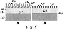
- the substrate (100) typically comprises a Si wafer (110) (which may typically comprise one or more semiconductor devices, such as transistors), a blocking layer (120) (e.g. a SiCO and/or SiCN layer), a low-k dielectric layer (130), a TiN hardmask memory layer (210) and a spacer material (220) (e.g. Si 3 N 4 , SiO 2 , AlN or TiO 2 ) defining the trenches (700).
- a barrier layer is typically present directly under it (not shown) and an oxide capping layer is typically present directly on it (not shown).
- a spin-on-carbon (SOC) first overlayer first overlayer.
- SOC spin-on-carbon
- SOG spin-on-glass layer
- the block pattern is transferred to the SOG, the SOC, and the HM, then the patterned HM is covered with a SOC layer, then with a masking layer consisting of an SOG layer and a photoresist, is provided thereon and a via pattern (i.e. a pattern for forming via openings) is defined in the photoresist.
- the via pattern is etched down to the SOG layer, the SOC layer and is etched further down to the HM.
- the via pattern and the blocked trench pattern are then etched further down into the low-k dielectric layer.
- the photoresist, the SOG layer and the SOC layer are consecutively stripped. This stripping may be performed as a separate step or it may occur as a consequence of etching down the pattern.
- the trench and via openings may be filled with a contact metal, e.g. using a damascene process.
- Fig. 8 Also depicted in Fig. 8 are optional additional steps (dashed outlines) which are performed when multiple block and/or multiple via patterning is desired. These optional steps include covering the SOC layer (of the first box of the flowchart and/or the seventh box of the flowchart) with multiple memory (hard mask) layers and a further SOC layer. In such cases, the process comprises, after opening the SOG and before opening the corresponding SOC, opening the further SOC layer and the multiple memory layers.
- this process entails many steps.
- the embodiments of the present invention permit to considerably reduce the number of steps as it will be illustrated in details in the following exemplary embodiments.
- Example 1 A first process flow for forming trench and via openings in a semiconductor structure
- a first process flow for forming trench and via openings in a semiconductor structure, using a method and structures according to the present invention, is described.
- the substrate (100) comprises a Si wafer (110) (which may typically comprise one or more semiconductor devices present at the lowest metallization level (Mo level) of the device, such as transistors, and/or may comprise M n-1 level metal conductive lines, wherein M n is the level corresponding to the conductive lines that will be enabled by the trenches (700)), a blocking layer (120) (e.g. a SiCO and/or SiCN layer), a low-k dielectric layer (130), a TiN hardmask memory layer (210) and a spacer material (220) (e.g.
- Si wafer (110) which may typically comprise one or more semiconductor devices present at the lowest metallization level (Mo level) of the device, such as transistors, and/or may comprise M n-1 level metal conductive lines, wherein M n is the level corresponding to the conductive lines that will be enabled by the trenches (700)
- a blocking layer 120
- a low-k dielectric layer 130
- TiN hardmask memory layer
- the substrate (100) comprises a Si wafer (110), a blocking layer (120) (e.g. a SiCO and/or SiCN layer), a low-k dielectric layer (130) and a condensed photo-condensable metal oxide (250) in which the trenches (700) are defined.
- a blocking layer 120
- a low-k dielectric layer 130
- a condensed photo-condensable metal oxide 250
- Fig. 2 The trenches (700) are filled and covered with a spin-on-carbon (SOC; 310) first overlayer (300) ( Fig. 2a ). Subsequently, a photo-condensable metal oxide layer is provided over the first overlayer (300) and a block pattern (400) is formed therein ( Fig. 2b ). The block pattern (400) is covered with a second overlayer (500) layer consisting of a spin-on-glass (SOG; 510) ( Fig. 2c ) and SOC layer (520) ( Fig. 2d ).
- SOG spin-on-glass
- SOC spin-on-glass
- a masking layer (600) consisting of an SOG layer (610) and a photoresist (620) is provided thereon and a via pattern (800) (i.e. a pattern for forming via openings) is defined in the photoresist (620) ( Fig. 2d ).
- the via pattern (800) is etched down to the SOG layer (510) of the second overlayer (500) and the photoresist (620) is removed ( Fig. 3a ).
- the via pattern (800) is etched further down to the hardmask memory layer (210) and the SOG (610) of the masking layer (600) and the SOC (520) of the second overlayer (500) are removed ( Fig. 3b ).
- the via pattern (800) is etched yet further down into the low-k dielectric layer (130), and the SOG (510) of the second overlayer (500) layer is removed ( Fig. 3c ).
- the first overlayer (300) is removed where it is not covered by the block pattern (400), thereby exposing trench portions (710) ( Fig. 3d ). These trench portions (710) are in turn etched down to the low-k dielectric layer (130), forming interruptions at the trench portions (720) present underneath the block pattern (400), and the block pattern (400) is removed ( Fig. 3e ). The remainder of the first overlayer (300) is removed ( Fig. 3f ). Finally, the trench (700) and via (800) patterns are etched further down, until the via openings expose part of the Si wafer (110) (typically until the via openings expose contacts to devices comprised in that substrate) or until the via openings expose M n-1 level metal conductive lines ( Fig. 3g ).
- the spacer material (220) and hardmask (210) may be removed and the trench and via openings may be filled with a contact metal, e.g. using a damascene process.
- the hardmask (210) can for example be removed by means of chemical mechanical polishing after the trench and via openings are filled with the contact metal.
- the masking layer (600) may consist of a photo-condensable metal oxide (650) and the via pattern (800) may be defined in the photo-condensable metal oxide (650).
- the other steps being analogous to what was already described with respect to Fig. 3 .
- Example 2 A second process flow for forming trench and via openings in a semiconductor structure
- a second process flow for forming trench and via openings in a semiconductor structure, using a method and structures according to the present invention, is described.
- the second overlayer (500) layer consists of an SOG layer.
- a masking layer (600) consisting of a photo-condensable metal oxide (650) is provided thereon and the via pattern (800) is defined in the photo-condensable metal oxide (650) ( Fig. 5a ).
- the via pattern (800) is etched down to the SOC (310) layer of the first overlayer (300) ( Fig. 5b ).
- the masking layer (600) is removed ( Fig. 5c ).
- the via pattern (800) is etched further down to the hardmask (210) ( Fig. 5d ). Further steps are as previously described in example 1 ( Fig. 3c-g ).
- Example 3 A third process flow for forming trench and via openings in a semiconductor structure
- a third process flow for forming trench and via openings in a semiconductor structure, using a method and structures according to the present invention, is described.
- the first overlayer (300) consists of an SOC layer (310) and an SOG layer (320) thereon, whereupon the condensed photo-condensable metal oxide block pattern (400) is formed ( Fig. 6a ).
- the block pattern (400) is covered with a second overlayer (500) consisting of an SOC layer (520) ( Fig. 6c ).
- a masking layer (600) comprising an SOG layer (610) and a photoresist (620) is provided thereon and a via pattern (800) is defined in the photoresist (620) ( Fig. 6c ).
- Example 4 A fourth process flow for forming trench and via openings in a semiconductor structure
- a fourth process flow for forming trench and via openings in a semiconductor structure, using a method and structures according to the present invention, is described.
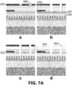
- Fig. 7 A similar structure as in example 3 is formed, but the masking layer (600) consists of a photo-condensable metal oxide (650) ( Fig. 7a ).
- the via pattern (800) is etched down to the SOG layer (320) of the first overlayer (300) ( Fig. 7b ), after which the SOG layer (320) is opened ( Fig. 7c ) and the masking layer (600) is removed ( Fig. 7d ).
- the via pattern (800) is etched further down to the memory layer (210) and the second overlayer (500) is removed ( Fig. 7e ).
- the SOG (320) of the first overlayer (300) is removed where it is not covered by the block pattern (400) ( Fig.
- the via pattern (800) is etched further down to the low-k dielectric layer (130) ( Fig. 7g ) and the SOC (310) of the first overlayer (300) is removed where it is not covered by the no patterned SOG layer (320) ( Fig. 7h ).
- the via pattern (800) is etched yet further down in to the low-k dielectric layer (130) and the remainder of the SOG (320) in the first overlayer (300) is removed ( Fig. 7i ).
- the exposed trench portions (710) are etched down to the low-k dielectric layer (130), forming interruptions corresponding to the trench portions which remain covered (720) ( Fig. 7j ). Further steps are as previously described in example 1 ( Fig. 3f-g ).
Landscapes
- Internal Circuitry In Semiconductor Integrated Circuit Devices (AREA)
- Drying Of Semiconductors (AREA)
- Chemical & Material Sciences (AREA)
- Inorganic Chemistry (AREA)
Abstract
A method for blocking one or more portions of one or more trenches (700) during manufacture of a semiconductor structure, the method comprising:
a. providing a substrate (100) comprising one or more trenches (700), and a dielectric material (130),
b. providing a first overlayer (300), thereby filling the one or more trenches (700);
c. covering a first area of the substrate (100), situated directly above the one or more portions and corresponding thereto, with a block pattern (400) of the condensed photo-condensable metal oxide;
d. covering the block pattern and the second area with a second overlayer (500);
e. providing a masking layer (600) over the second overlayer (500), the masking layer (600) having a via pattern (800); and
f. transferring the via pattern (800) and the other portion of the at least one of the trenches (700) into the dielectric material (130).
a. providing a substrate (100) comprising one or more trenches (700), and a dielectric material (130),
b. providing a first overlayer (300), thereby filling the one or more trenches (700);
c. covering a first area of the substrate (100), situated directly above the one or more portions and corresponding thereto, with a block pattern (400) of the condensed photo-condensable metal oxide;
d. covering the block pattern and the second area with a second overlayer (500);
e. providing a masking layer (600) over the second overlayer (500), the masking layer (600) having a via pattern (800); and
f. transferring the via pattern (800) and the other portion of the at least one of the trenches (700) into the dielectric material (130).
Description
- The present invention relates to manufacturing of semiconductor structures and in particular to blocking one or more trench portions during said manufacturing.
- In the manufacture of semiconductor devices, especially on advanced nodes, multiple lithographic layer stacks and mulitple lithographic exposure and etch sequences are required for forming vias and connecting lines in the Back End Of Line (BEOL).
- A typical sequence for the formation of such connecting lines is described in Kobayashi, Shinji, et al. "Analyzing block placement errors in SADP patterning." Proc. Of SPIE Vol 9779, 2016. This sequence starts by forming a pattern of spacer-defined trenches, followed by providing a lithographic stack and performing a first lithographic exposure and etch sequence to form blocks above portions of the trenches. Subsequently, the trench pattern is etched deeper into the substrate, such as into a hard mask layer in the substrate, whereby the blocks define interruptions in the trenches.
- Once the wished interrupted trench pattern is transferred in the hard mask, in order to form vias, it is typical to use a second lithographic stack and a second lithographic exposure and etch sequence to pattern vias into the hard mask. After both the via and trench patterns have been etched to the appropriate depth in the dielectric underlying the hard mask, the corresponding openings may be filled with a conductive metal to form the vias and connecting lines. A flowchart of this process up to the etching in the dielectric is shown in
Fig. 8 . - There is still room in the art for more straightforward BEOL methods.
- It is an object of the present invention to provide good methods and structures for BEOL.
- It is an advantage of embodiments of the present invention that a low number of steps is required.
- The above objective is accomplished by a method and device according to the present invention.
- In a first aspect, the present invention relates to a method for blocking one or more portions of one or more trenches during manufacture of a semiconductor structure, the method comprising:
- a. providing a substrate comprising one or more trenches, and a dielectric material under the one or more trenches,
- b. providing a first overlayer on the substrate, thereby filling the one or more trenches, the first overlayer having a planar top surface, a top portion of the first overlayer, comprising the top surface, being etchable selectively with respect to a condensed photo-condensable metal oxide;
- c. covering a first area of the top surface, situated directly above the one or more portions and corresponding thereto, with a block pattern of the condensed photo-condensable metal oxide, thereby leaving a second area of the top surface, having at least another portion of at least one of the trenches thereunder, uncovered;
- d. covering the block pattern and the second area with a second overlayer having a planar top surface, a bottom portion of the second overlayer, in contact with the block pattern and the second area, being etchable selectively with respect to the condensed photo-condensable metal oxide and with respect to the top portion of the first overlayer;
- e. providing a masking layer over the second overlayer, the masking layer having a via pattern; and
- f. transferring the via pattern and the other portion of the at least one of the trenches into the dielectric material.
- In a second aspect, the present invention relates to a semiconductor structure, comprising:
- i. a substrate comprising one or more trenches, and a dielectric material under the one or more trenches;
- ii. a first overlayer on the substrate, filling the one or more trenches and having a planar top surface, a top portion of the first overlayer, comprising the top surface, being etchable selectively with respect to a condensed photo-condensable metal oxide;
- iii. a block pattern of a condensed photo-condensable metal oxide, the block pattern covering a first area of the top surface, the first area being situated directly above one or more portions of the one or more trenches and corresponding to these portions, a second area of the top surface, having at least another portion of at least one of the trenches thereunder, remaining uncovered; and
- iv. a second overlayer having a planar top surface, a bottom portion of the second overlayer, in contact with the block pattern and the second area, being etchable selectively with respect to the condensed photo-condensable metal oxide and with respect to the top portion of the first overlayer.
- Particular and preferred aspects of the invention are set out in the accompanying independent and dependent claims. Features from the dependent claims may be combined with features of the independent claims and with features of other dependent claims as appropriate and not merely as explicitly set out in the claims.
- Although there has been constant improvement, change and evolution of devices in this field, the present concepts are believed to represent substantial new and novel improvements, including departures from prior practices, resulting in the provision of more efficient, stable and reliable devices of this nature.
- The above and other characteristics, features and advantages of the present invention will become apparent from the following detailed description, taken in conjunction with the accompanying drawings, which illustrate, by way of example, the principles of the invention. This description is given for the sake of example only, without limiting the scope of the invention. The reference figures quoted below refer to the attached drawings.
-
-
Figs. 1 a and b are schematic representations of vertical cross-sections of two substrates used in accordance with embodiments of the present invention. -
Figs. 2 to 3 are schematic representations of vertical cross-sections of semiconductor structures obtained at different stages of manufacture in accordance with an embodiment of the present invention starting withFig. 1a . -
Fig. 4 is a schematic representation of a vertical cross-section of a semiconductor structure obtained when a condensed photo-condensable metal oxide masking layer is used to replace the masking layer provided inFig.2 (d) . -
Fig. 5 is a schematic representation of vertical cross-sections obtained at different stages of manufacture in accordance with another embodiment of the present invention. -
Fig. 6 is a schematic representation of vertical cross-sections obtained at different stages of manufacture in accordance with yet another embodiment of the present invention. -
Fig. 7 is a schematic representation of vertical cross-sections obtained at different stages of manufacture in accordance with yet a further embodiment of the present invention. -
Fig. 8 is a flowchart showing the main steps in a process of the prior art. -
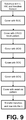
Fig. 9 is a flowchart showing the main steps of a process in accordance with the embodiment of the present invention illustrated inFigs. 2 to 3 . -
Fig. 10 is a flowchart showing the main steps of a process in accordance with the embodiment illustrated inFig. 4 where a condensed photo-condensable metal oxide masking layer is used to replace the masking layer provided inFig.2(d) . -
Fig. 11 is a flowchart showing the main steps of a process in accordance with the other embodiment of the present invention illustrated inFig. 5 . -
Fig. 12 is a flowchart showing the main steps of a process in accordance with the yet other embodiment of the present invention illustrated inFig. 6 . -
Fig. 13 is a flowchart showing the main steps of a process in accordance with the yet further embodiment illustrated inFig. 7 . - In the different figures, the same reference signs refer to the same or analogous elements.
- The present invention will be described with respect to particular embodiments and with reference to certain drawings but the invention is not limited thereto but only by the claims. The drawings described are only schematic and are non-limiting. In the drawings, the size of some of the elements may be exaggerated and not drawn on scale for illustrative purposes. The dimensions and the relative dimensions do not correspond to actual reductions to practice of the invention.
- Furthermore, the terms first, second, third and the like in the description and in the claims, are used for distinguishing between similar elements and not necessarily for describing a sequence, either temporally, spatially, in ranking or in any other manner. It is to be understood that the terms so used are interchangeable under appropriate circumstances and that the embodiments of the invention described herein are capable of operation in other sequences than described or illustrated herein.
- Moreover, the terms top, bottom, over, under and the like in the description and the claims are used for descriptive purposes and not necessarily for describing relative positions. It is to be understood that the terms so used are interchangeable under appropriate circumstances and that the embodiments of the invention described herein are capable of operation in other orientations than described or illustrated herein.
- It is to be noticed that the term "comprising", used in the claims, should not be interpreted as being restricted to the means listed thereafter; it does not exclude other elements or steps. It is thus to be interpreted as specifying the presence of the stated features, integers, steps or components as referred to, but does not preclude the presence or addition of one or more other features, integers, steps or components, or groups thereof. Thus, the scope of the expression "a device comprising means A and B" should not be limited to devices consisting only of components A and B. It means that with respect to the present invention, the only relevant components of the device are A and B.
- Reference throughout this specification to "one embodiment" or "an embodiment" means that a particular feature, structure or characteristic described in connection with the embodiment is included in at least one embodiment of the present invention. Thus, appearances of the phrases "in one embodiment" or "in an embodiment" in various places throughout this specification are not necessarily all referring to the same embodiment, but may. Furthermore, the particular features, structures or characteristics may be combined in any suitable manner, as would be apparent to one of ordinary skill in the art from this disclosure, in one or more embodiments.
- Similarly it should be appreciated that in the description of exemplary embodiments of the invention, various features of the invention are sometimes grouped together in a single embodiment, figure, or description thereof for the purpose of streamlining the disclosure and aiding in the understanding of one or more of the various inventive aspects. This method of disclosure, however, is not to be interpreted as reflecting an intention that the claimed invention requires more features than are expressly recited in each claim. Rather, as the following claims reflect, inventive aspects lie in less than all features of a single foregoing disclosed embodiment. Thus, the claims following the detailed description are hereby expressly incorporated into this detailed description, with each claim standing on its own as a separate embodiment of this invention.
- Furthermore, while some embodiments described herein include some but not other features included in other embodiments, combinations of features of different embodiments are meant to be within the scope of the invention, and form different embodiments, as would be understood by those in the art. For example, in the following claims, any of the claimed embodiments can be used in any combination.
- Furthermore, some of the embodiments are described herein as a method or combination of elements of a method that can be implemented by a processor of a computer system or by other means of carrying out the function. Thus, a processor with the necessary instructions for carrying out such a method or element of a method forms a means for carrying out the method or element of a method. Furthermore, an element described herein of an apparatus embodiment is an example of a means for carrying out the function performed by the element for the purpose of carrying out the invention.
- In the description provided herein, numerous specific details are set forth. However, it is understood that embodiments of the invention may be practiced without these specific details. In other instances, well-known methods, structures and techniques have not been shown in detail in order not to obscure an understanding of this description.
- The following term is provided solely to aid in the understanding of the invention.
- As used herein, when a first material is said to be etched selectively with respect to a second material, this means that the first material is etched faster than the second material. Preferably, the etching process would etch the first material at least twice faster, or more preferably at least five times faster, yet more preferably at least 10 times faster, than the second material. In some preferred embodiments, the second material may be substantially not etched by the etching process.
- As used herein, and unless provided otherwise, the term metal encompasses alkali metals, alkaline earth metals, transition metals, post-transition metals, lanthanides and actinides. It excludes metalloids (B, Si, Ge As, Sb, Te) and non-metals (C, P, S, Se, H, N, O, F, Cl, Br, I, and noble gases).
- In a first aspect, the present invention relates to a method for blocking one or more portions of one or more trenches during manufacture of a semiconductor structure, the method comprising:
- a. providing a substrate comprising one or more trenches, and a dielectric material under the one or more trenches,
- b. providing a first overlayer on the substrate, thereby filling the one or more trenches, the first overlayer having a planar top surface, a top portion of the first overlayer, comprising the top surface, being etchable selectively with respect to a condensed photo-condensable metal oxide;
- c. covering a first area of the top surface, situated directly above the one or more portions and corresponding thereto, with a block pattern of the condensed photo-condensable metal oxide, thereby leaving a second area of the top surface, having at least another portion of at least one of the trenches thereunder, uncovered;
- d. covering the block pattern and the second area with a second overlayer having a planar top surface, a bottom portion of the second overlayer, in contact with the block pattern and the second area, being etchable selectively with respect to the condensed photo-condensable metal oxide and with respect to the top portion of the first overlayer;
- e. providing a masking layer over the second overlayer, the masking layer having a via pattern; and
- f. transferring the via pattern and the other portion of the at least one of the trenches into the dielectric material.
- In step a of the method, a substrate is provided. The substrate comprises one or more trenches and a dielectric material under the one or more trenches.
- In embodiments, directly under the trenches, the substrate may comprise a hardmask. This hardmask will aslo hereinafter be called "memory layer" since it records the trench and via pattern. This hardmask would therefore form the bottom of the trenches. A hardmask directly under the trenches is advantageous in embodiments where the material used to form the sidewalls of the trenches is not sufficiently etch-resistant to survive the entire trench and via transfer process. This will typically be the case when the trenches are defined in a spacer material (e.g. Si3N4, SiO2, AlN or TiO2), for example formed therein using an ArF lithography, an EUV lithography or a spacer defined technology. The hardmask may for instance be a TiN layer.
- A hardmask is however superfluous if the sidewalls of the trenches are defined in a condensed photo-condensable metal oxide. Indeed, condensed photo-condensable metal oxides are typically sufficiently etch-resistant to survive the entire trench and via transfer process.
- In embodiments, which are preferred, the substrate may therefore further comprise a condensed photo-condensable metal oxide layer in which the sidewalls of the one or more trenches are defined.
- In general, an advantage of a photo-condensable metal oxide layer is that it can be easily patterned, e.g. in a fashion analogous to how a photoresist can be patterned using an EUV lithography, while being hard enough to suitably resist against being etched during the process of transferring trenches and vias in the dielectric layer. As such, a condensed photo-condensable metal oxide layer combines the advantages of a hardmask and of a photoresist into a single layer.
- Typically, directly under the hardmask, or directly under the trenches if no hardmask is present, the substrate comprise the dielectric layer. Hence, if the trenches have condensed photo-condensable metal oxide side walls, the bottom of the trenches will typically be made of the dielectric layer. The dielectric layer is preferably a low-k dielectric layer. The deepening of the trenches is typically stopped in this dielectric layer.
- Directly under the dielectric layer, the substrate may typically comprise a blocking layer such as a SiCO and/or SiCN layer.
- Directly under the blocking layer, the substrate may typically further comprise a semiconductive part, such as a semiconductor (e.g. Si) wafer. The semiconductive part may typically comprise semiconductor devices such as transistors forming a so-called M0 level, and the trenches will be used to form conductive lines at a so-called M1 level, with the vias connecting part of the M1 level with part of the M0 level. The invention may however also be used to connect a Mn+1 level with the underlying Mn level, where n is an integer equal to at least 1.
- In step b, the first overlayer fills the one or more trenches.
- The first overlayer advantageously provides a planarization of the device under construction by completely filling the one or more trenches and presenting a planar top surface. In embodiments, filling the one or more trenches may comprise overfilling the one or more trenches. By overfilling the one or more trenches, a first overlayer is typically formed which uniformly covers an area of the substrate, including a surface of the substrate in between two trenches. In embodiments, the first overlayer may be planarized by using a chemical-mechanical polishing.
- In embodiments, the first overlayer may comprise a single layer or a plurality of sub-layers. Preferably it consists of one or two layers. Preferably, it comprises a planarization layer filling completely the one or more trenches and, optionally, a hardmask layer thereon. In embodiments, the planarization layer may be a spin-on-carbon layer (SOC). In embodiments, the optional hardmask layer may be a spin-on-glass (SOG), a SiO2, a SiOC or a Si3N4 layer. In embodiments, after step d, the second overlayer may be directly in contact with the first overlayer; i.e. an area exists where the first overlayer and the second overlayer are not separated by any further layers. In preferred embodiments, the contact may consist of a contact between two different materials. The optional hardmask layer is typically used to advantageously provide this contact between two different materials, when at least a top surface of the planarization layer and a bottom surface of the second overlayer consist of the same material.
- The trench referred to in the present invention is typically a concave shape in the substrate, which is longer than wide. The substrate will typically have more than one of such trenches. They are typically disposed parallel to each other. They are typically placed at a regular interval following a certain pitch. In embodiments, the substrate may comprise two or more trenches disposed with a pitch of 45 nm or less, preferably 30 nm or less, such as 20 nm or less. The pitch is defined as being the distance between a longitudinal side of a trench and the corresponding longitudinal side of a neighbouring trench. The pitch is therefore equal to the distance between two trenches plus the width of a trench. In embodiments, the one or more trenches may have a width of 25 nm or less, preferably 13 nm or less, such as 9.5 nm or less. In embodiments, the one or more trenches may be formed using an ArF lithography, an EUV lithography or a spacer defined technology such as self-aligned multiple patterning (SAMP). Examples of SAMP are self-aligned double patterning (SADP), self-aligned quadruple patterning (SAQP), and self-aligned octuple patterning (SAOP). In the case of a spacer defined technology, the side-walls of the trenches are the side-walls of the spacers and the bottom of the trenches is part of the top surface of the layer directly underlying the spacers. The layer directly underlying the spacers is typically a hardmask layer such as TiN.
- In the method of the present invention, the trenches in the substrate may be longer than required for the particular envisioned connection scheme. Hence, the blocking of portions of these trenches may fulfil the purpose of precisely limiting the length of the trenches to the requirements of the connection scheme. The portion referred to in the present invention is a segment of a trench along its length. It is defined by the entire width of the trench and by only part of its length. Blocking a portion means entirely covering that trench portion with a block pattern, and leaving the rest of that trench uncovered, so as to prevent that portion of the trench to be ultimately transferred into the dielectric material. Hence, in step f, the transfer of the other portion of the at least one of the trenches into the dielectric material will create therein two co-linear trenches linearly separated by a distance corresponding to the length of the portion of the original trench which has been blocked. It is an advantage of embodiments of the present invention that these two new co-linear trenches have well-defined length, determined by the position of the blocked portion. The deepening of the trenches can for instance comprise first the transfer of the blocked trench pattern into a hardmask underlying the original trenches, followed by a transfer of the pattern now present in the hardmask to the underlying dielectric layer of the substrate, such as a low-k dielectric layer. These trenches in the dielectric layer can then be metalized to serve as connecting lines.
- The method of the present invention is typically used during manufacture of a semiconductor device, such as a device comprising one or more field effect transistors at a M0 level. The method of the present invention can for instance be used to form connecting lines at a M1 level and vias connecting these lines with contacts at a M0 level.
- Typically, step f comprises transferring the via pattern down to the bottom of the dielectric layer, in the blocking layer if present, in order to expose a portion of the semiconductive part to which the via will allow an electrical connection to be made.
- The trenches and the vias in the present method are typically used in interconnecting different parts of the semiconductor device.
- In embodiments, the method may further comprise, after step f:
- g. filling at least partially the trenches and the vias in the dielectric layer with a conductive material.
- The conductive material may be a metal, such as copper, cobalt, ruthenium or NiSi. The trenches and/or the vias may be lined with one or more barrier layers prior to filling it with the conductive material. Filling the at least one opening with the conductive material typically forms connecting lines and vias and may for example comprise a damascene or dual damascene process.
- The block pattern is made of a condensed photo-condensable metal oxide. Since it is made of a metal oxide, it typically has different etching properties than typical photoresists, that are organic materials, and different etching properties than traditional hardmasks such as non-oxide hardmasks (e.g. TiN or Si3N4) or hardmasks which comprise oxygen but no metal (e.g. comprising a metalloid such as Si instead of a metal, like in the case of SOG or SiOC). This permits mutual selective etching among 1) the condensed photo-condensable metal oxide, 2) an organic material (e.g. a polymer such as a SOC material or an organic photoresist), and 3) a hard mask which is not a metal oxide (e.g. a non-oxide hardmasks or a hardmask which comprise oxygen but no metal). The metal oxide is a photo-condensable metal oxide. A photo-condensable metal oxide may also be referred to as a photo-condensable molecular metal oxide. "Photo-condensable" means that it can be condensed, i.e. hardened, upon exposure to a suitable light. As such, it behaves like a photoresist but is typically much more etch resistant than traditional photoresists. The block pattern is formed of condensed photo-condensable metal oxide, i.e. photo-condensable metal oxide that has been condensed by exposure to a suitable light, e.g. EUV light.
- The condensed photo-condensable metal oxide is advantageously easily patterned, e.g. as a block pattern, while being etch resistant enough to suitably resist against etching during etching of the first and second overlayers (e.g. during step f of transferring the pattern), and in particular during etching of the first overlayer. As such, the condensed photo-condensable metal oxide combines the advantages of a separate hardmask layer and a separate photoresist layer into a single layer. Patterning the photo-condensable metal oxide may for example be done using an EUV lithography to condense a pattern within an uncondensed photo-condensable metal oxide. In embodiments, the first overlayer may be etchable selectively with respect to the condensed photo-condensable metal oxide. In other words, at least one etching chemistry may exist which etches the first overlayer selectively with respect to the condensed photo-condensable metal oxide.
- In embodiments, step c may comprise:
- c1. providing a layer of a photo-condensable metal oxide;
- c2. exposing an area of the layer of photo-condensable metal oxide to a light source, such that the area of the layer condenses into the block pattern of condensed photo-condensable metal oxide; and
- c3. removing any uncondensed photo-condensable metal oxide.
- A condensed photo-condensable metal oxide is obtained after irradiation at a suitable wavelength for the photo-condensable metal oxide. For instance, the photo-condensable metal oxide may be condensable under EUV irradiation.
- In embodiments, one or more of the photo-condensable metal oxides used in embodiments of the present invention may comprise an organo-tin compound.
- In embodiments, the organo-tin compound may be an organometallic compound having a general chemical formula of RSnO(3/2-x/2)(OH)x where (0<x<3), where R is an alkyl group or cycloalkyl group with 3-31 carbon atoms, where the alkyl or cycloalkyl group is bonded to the tin at a secondary or tertiary carbon atom, as described in
WO2016065120 , the content of which being incorporated herein by reference. - In embodiments, the photo-condensable metal oxides may comprise or be a metal oxo-hydroxo network with organic ligands with a metal carbon bonds and/or with metal carboxylate bonds, as described in
WO 2015/026482 , the content of which being incorporated herein by reference. - In embodiments, the photo-condensable metal oxide may comprise or be a metal oxide hardmask formed from an aqueous hardmask precursor composition comprising polyoxometal clusters and polyatomic inorganic anions, as described in
WO 2012/118847 , the content of which being incorporated herein by reference. - In embodiments, the photo-condensable metal oxide may be a composition comprising metal suboxide cations, ligands comprising a peroxide group and inorganic polyatomic anions, wherein the composition has a molar concentration ratio of ligands to metal suboxide cations of at least about 2, as described in
EP2392969 , the content of which being incorporated herein by reference. - In embodiments, the second overlayer may comprise a spin-on-glass layer and/or a spin-on-carbon layer. The second overlayer may typically consist of a spin-on-glass layer and/or a spin-on-carbon layer. In embodiments, the second overlayer may consist of a single material. In embodiments, after step e, the second overlayer may be directly in contact with the masking layer, with the block pattern and with the second area of the substrate.
- In embodiments, steps c and d may be repeated one or more times. In that case, the top surface referred to in the repeated step c refers to the top surface of the last deposited overlayer (e.g. the top surface of the second overlayer deposited in the first step d if it is the first time step c is repeated).
- In embodiments, the masking layer may comprise a photoresist layer or a condensed photo-condensable metal oxide layer. In preferred embodiments, the masking layer may consist of the combination of a photoresist patterned layer and a hardmask thereunder or may consist of a condensed photo-condensable metal oxide layer. Any chemically amplified resist may typically be suitable for forming the masking layer. In preferred embodiments, the masking layer may be an EUV masking layer. The via pattern is typically formed in the masking layer using a suitable lithographic procedure, such as using an EUV lithography.
- In preferred embodiments, step f may comprise: transferring the via pattern into the dielectric layer, removing the masking layer, removing the second overlayer, and etching away the first overlayer present over the second area selectively with respect to the first area by using the block pattern as an etching mask.
- In a first set of embodiments, the first overlayer may consist of a spin-on-carbon planarization layer, the second overlayer may consist of a spin-on-glass layer and a spin-on-carbon layer thereon, and the masking layer may consist of a spin-on-glass layer and a photoresist layer thereon.
- In a second set of embodiments, the first overlayer may consist of a spin-on-carbon planarization layer, the second overlayer may consist of a spin-on-glass layer and a spin-on-carbon layer thereon, and the masking layer may consist of a condensed photo-condensable metal oxide layer.
- In a third set of embodiments, the first overlayer may consist of a spin-on-carbon planarization layer, the second overlayer may consist of a spin-on-glass layer, and the masking layer may consist of a condensed photo-condensable metal oxide layer.
- In a fourth set of embodiments, the first overlayer may consist of a spin-on-carbon planarization layer and a spin-on-glass hardmask layer thereon, the second overlayer may consist of a spin-on-glass layer, and the masking layer may consist of a spin-on-glass layer and a photoresist layer thereon.
- In a fifth set of embodiments, the first overlayer may consist of a spin-on-carbon planarization layer and a spin-on-glass hardmask layer thereon, the second overlayer may consist of a spin-on-glass layer, and the masking layer may consist of a condensed photo-condensable metal oxide layer.
- In a second aspect, the present invention relates to a semiconductor structure, comprising:
- i. a substrate comprising one or more trenches, and a dielectric material under the one or more trenches,
- ii. a first overlayer on the substrate, filling the one or more trenches and having a planar top surface, a top portion of the first overlayer, comprising the top surface, being etchable selectively with respect to a condensed photo-condensable metal oxide;
- iii. a block pattern of a condensed photo-condensable metal oxide, the block pattern covering a first area of the top surface, the first area being situated directly above one or more portions of the one or more trenches and corresponding to these portions, a second area of the top surface, having at least another portion of at least one of the trenches thereunder, remaining uncovered; and
- iv. a second overlayer having a planar top surface, a bottom portion of the second overlayer, in contact with the block pattern and the second area, being etchable selectively with respect to the condensed photo-condensable metal oxide and with respect to the top portion of the first overlayer;
- In embodiments, the structure may further comprise:
- v. a masking layer over the second overlayer, wherein the masking layer has a via pattern.
- In embodiments, the structure may further comprise:
- vi. trenches and vias in the dielectric material. The masking layer is typically no longer present in that embodiment.
- In a first set of embodiments, the first overlayer may consist of a spin-on-carbon planarization layer, the second overlayer may consist of a spin-on-glass layer and a spin-on-carbon layer thereon, and the masking layer, if present, may consist of a spin-on-glass layer and a photoresist layer thereon.
- In a second set of embodiments, the first overlayer may consist of a spin-on-carbon planarization layer, the second overlayer may consist of a spin-on-glass layer and a spin-on-carbon layer thereon, and the masking layer, if present, may consist of a condensed photo-condensable metal oxide layer.
- In a third set of embodiments, the first overlayer may consist of a spin-on-carbon planarization layer, the second overlayer may consist of a spin-on-glass layer, and the masking layer, if present, may consist of a condensed photo-condensable metal oxide layer.
- In a fourth set of embodiments, the first overlayer may consist of a spin-on-carbon planarization layer and a spin-on-glass hardmask layer thereon, the second overlayer may consist of a spin-on-glass layer, and the masking layer, if present, may consist of a spin-on-glass layer and a photoresist layer thereon.
- In a fifth set of embodiments, the first overlayer may consist of a spin-on-carbon planarization layer and a spin-on-glass hardmask layer thereon, the second overlayer may consist of a spin-on-glass layer, and the masking layer, if present, may consist of a condensed photo-condensable metal oxide layer.
- In any embodiment, any feature of the second aspect and its embodiments may independently be as correspondingly described for the first aspect and its embodiments.
- The invention will now be described by a detailed description of several embodiments of the invention. It is clear that other embodiments of the invention can be configured according to the knowledge of the person skilled in the art without departing from the true technical teaching of the invention, the invention being limited only by the terms of the appended claims.
- Reference will be made to transistors. These are (three-terminal) devices having a first main electrode such as a drain, a second main electrode such as a source and a control electrode such as a gate for controlling the flow of electrical charges between the first and second main electrodes.
- We now refer to
Fig. 8 . - A substrate comprising trenches, a hardmask (HM) thereunder and a dielectric layer (ε) under the hardmask (HM) is provided. We now refer to
Fig 1 a. The substrate (100) typically comprises a Si wafer (110) (which may typically comprise one or more semiconductor devices, such as transistors), a blocking layer (120) (e.g. a SiCO and/or SiCN layer), a low-k dielectric layer (130), a TiN hardmask memory layer (210) and a spacer material (220) (e.g. Si3N4, SiO2, AlN or TiO2) defining the trenches (700). In addition to the low-k dielectric layer (130), a barrier layer is typically present directly under it (not shown) and an oxide capping layer is typically present directly on it (not shown). - We now turn back to
Fig. 8 . The trenches are filled and covered with a spin-on-carbon (SOC) first overlayer. Subsequently, a spin-on-glass layer (SOG) is provided over the SOC layer and a photoresist block pattern is formed thereon. The block pattern is transferred to the SOG, the SOC, and the HM, then the patterned HM is covered with a SOC layer, then with a masking layer consisting of an SOG layer and a photoresist, is provided thereon and a via pattern (i.e. a pattern for forming via openings) is defined in the photoresist. - The via pattern is etched down to the SOG layer, the SOC layer and is etched further down to the HM. The via pattern and the blocked trench pattern are then etched further down into the low-k dielectric layer. During these pattern transfers, the photoresist, the SOG layer and the SOC layer are consecutively stripped. This stripping may be performed as a separate step or it may occur as a consequence of etching down the pattern.
- In further steps, which are not depicted, the trench and via openings may be filled with a contact metal, e.g. using a damascene process.
- Also depicted in
Fig. 8 are optional additional steps (dashed outlines) which are performed when multiple block and/or multiple via patterning is desired. These optional steps include covering the SOC layer (of the first box of the flowchart and/or the seventh box of the flowchart) with multiple memory (hard mask) layers and a further SOC layer. In such cases, the process comprises, after opening the SOG and before opening the corresponding SOC, opening the further SOC layer and the multiple memory layers. - As can be seen in this flowchart, this process entails many steps. The embodiments of the present invention permit to considerably reduce the number of steps as it will be illustrated in details in the following exemplary embodiments.
- A first process flow for forming trench and via openings in a semiconductor structure, using a method and structures according to the present invention, is described.
- We now refer to
Fig. 1 . A substrate (100) comprising trenches (700) is provided. In a first version, seeFig. 1a , the substrate (100) comprises a Si wafer (110) (which may typically comprise one or more semiconductor devices present at the lowest metallization level (Mo level) of the device, such as transistors, and/or may comprise Mn-1 level metal conductive lines, wherein Mn is the level corresponding to the conductive lines that will be enabled by the trenches (700)), a blocking layer (120) (e.g. a SiCO and/or SiCN layer), a low-k dielectric layer (130), a TiN hardmask memory layer (210) and a spacer material (220) (e.g. Si3N4, SiO2, AlN or TiO2) defining the trenches (700). In an alternative version, seeFig. 1b , the substrate (100) comprises a Si wafer (110), a blocking layer (120) (e.g. a SiCO and/or SiCN layer), a low-k dielectric layer (130) and a condensed photo-condensable metal oxide (250) in which the trenches (700) are defined. - We now refer to
Fig. 2 . The trenches (700) are filled and covered with a spin-on-carbon (SOC; 310) first overlayer (300) (Fig. 2a ). Subsequently, a photo-condensable metal oxide layer is provided over the first overlayer (300) and a block pattern (400) is formed therein (Fig. 2b ). The block pattern (400) is covered with a second overlayer (500) layer consisting of a spin-on-glass (SOG; 510) (Fig. 2c ) and SOC layer (520) (Fig. 2d ). A masking layer (600) consisting of an SOG layer (610) and a photoresist (620) is provided thereon and a via pattern (800) (i.e. a pattern for forming via openings) is defined in the photoresist (620) (Fig. 2d ). - We now refer to
Fig. 3 . The via pattern (800) is etched down to the SOG layer (510) of the second overlayer (500) and the photoresist (620) is removed (Fig. 3a ). The via pattern (800) is etched further down to the hardmask memory layer (210) and the SOG (610) of the masking layer (600) and the SOC (520) of the second overlayer (500) are removed (Fig. 3b ). The via pattern (800) is etched yet further down into the low-k dielectric layer (130), and the SOG (510) of the second overlayer (500) layer is removed (Fig. 3c ). The first overlayer (300) is removed where it is not covered by the block pattern (400), thereby exposing trench portions (710) (Fig. 3d ). These trench portions (710) are in turn etched down to the low-k dielectric layer (130), forming interruptions at the trench portions (720) present underneath the block pattern (400), and the block pattern (400) is removed (Fig. 3e ). The remainder of the first overlayer (300) is removed (Fig. 3f ). Finally, the trench (700) and via (800) patterns are etched further down, until the via openings expose part of the Si wafer (110) (typically until the via openings expose contacts to devices comprised in that substrate) or until the via openings expose Mn-1 level metal conductive lines (Fig. 3g ). - In further steps, which are not depicted, the spacer material (220) and hardmask (210) may be removed and the trench and via openings may be filled with a contact metal, e.g. using a damascene process. The hardmask (210) can for example be removed by means of chemical mechanical polishing after the trench and via openings are filled with the contact metal.
- We now refer to
Fig. 4 . In an alternative version of this first example, the masking layer (600) may consist of a photo-condensable metal oxide (650) and the via pattern (800) may be defined in the photo-condensable metal oxide (650). The other steps being analogous to what was already described with respect toFig. 3 . - A second process flow for forming trench and via openings in a semiconductor structure, using a method and structures according to the present invention, is described.
- We now refer to
Fig. 5 . The same process flow as in example 1 is followed up to the stage depicted inFig. 2c . In this example, the second overlayer (500) layer consists of an SOG layer. A masking layer (600) consisting of a photo-condensable metal oxide (650) is provided thereon and the via pattern (800) is defined in the photo-condensable metal oxide (650) (Fig. 5a ). The via pattern (800) is etched down to the SOC (310) layer of the first overlayer (300) (Fig. 5b ). The masking layer (600) is removed (Fig. 5c ). Subsequently, the via pattern (800) is etched further down to the hardmask (210) (Fig. 5d ). Further steps are as previously described in example 1 (Fig. 3c-g ). - A third process flow for forming trench and via openings in a semiconductor structure, using a method and structures according to the present invention, is described.
- We now refer to
Fig. 6 . In this case, the first overlayer (300) consists of an SOC layer (310) and an SOG layer (320) thereon, whereupon the condensed photo-condensable metal oxide block pattern (400) is formed (Fig. 6a ). The block pattern (400) is covered with a second overlayer (500) consisting of an SOC layer (520) (Fig. 6c ). A masking layer (600) comprising an SOG layer (610) and a photoresist (620) is provided thereon and a via pattern (800) is defined in the photoresist (620) (Fig. 6c ). - Further steps (not depicted) are analogous to those described in example 4 (
Fig. 7b-j ). - A fourth process flow for forming trench and via openings in a semiconductor structure, using a method and structures according to the present invention, is described.
- We now refer to
Fig. 7 . A similar structure as in example 3 is formed, but the masking layer (600) consists of a photo-condensable metal oxide (650) (Fig. 7a ). The via pattern (800) is etched down to the SOG layer (320) of the first overlayer (300) (Fig. 7b ), after which the SOG layer (320) is opened (Fig. 7c ) and the masking layer (600) is removed (Fig. 7d ). The via pattern (800) is etched further down to the memory layer (210) and the second overlayer (500) is removed (Fig. 7e ). The SOG (320) of the first overlayer (300) is removed where it is not covered by the block pattern (400) (Fig. 7f ). The via pattern (800) is etched further down to the low-k dielectric layer (130) (Fig. 7g ) and the SOC (310) of the first overlayer (300) is removed where it is not covered by the no patterned SOG layer (320) (Fig. 7h ). The via pattern (800) is etched yet further down in to the low-k dielectric layer (130) and the remainder of the SOG (320) in the first overlayer (300) is removed (Fig. 7i ). The exposed trench portions (710) are etched down to the low-k dielectric layer (130), forming interruptions corresponding to the trench portions which remain covered (720) (Fig. 7j ). Further steps are as previously described in example 1 (Fig. 3f-g ). - It is to be understood that although preferred embodiments, specific constructions and configurations, as well as materials, have been discussed herein for devices according to the present invention, various changes or modifications in form and detail may be made without departing from the scope and technical teachings of this invention. For example, any formulas given above are merely representative of procedures that may be used. Functionality may be added or deleted from the block diagrams and operations may be interchanged among functional blocks. Steps may be added or deleted to methods described within the scope of the present invention.
Claims (14)
- A method for blocking one or more portions of one or more trenches (700) during manufacture of a semiconductor structure, the method comprising:a. providing a substrate (100) comprising one or more trenches (700), and a dielectric material (130) under the one or more trenches (700),b. providing a first overlayer (300) on the substrate (100), thereby filling the one or more trenches (700), the first overlayer (300) having a planar top surface, a top portion of the first overlayer (300), comprising the top surface, being etchable selectively with respect to a condensed photo-condensable metal oxide;c. covering a first area of the top surface, situated directly above the one or more portions and corresponding thereto, with a block pattern (400) of the condensed photo-condensable metal oxide, thereby leaving a second area of the top surface, having at least another portion of at least one of the trenches (700) thereunder, uncovered;d. covering the block pattern and the second area with a second overlayer (500) having a planar top surface, a bottom portion of the second overlayer (500), in contact with the block pattern and the second area, being etchable selectively with respect to the condensed photo-condensable metal oxide and with respect to the top portion of the first overlayer (300);e. providing a masking layer (600) over the second overlayer (500), the masking layer (600) having a via pattern (800); andf. transferring the via pattern (800) and the other portion of the at least one of the trenches (700) into the dielectric material (130).
- The method according to claim 1, wherein, after step d, the second overlayer (500) is directly in contact with the first overlayer (300).
- The method according to claim 1 or 2, wherein the first overlayer (300) comprises a planarization layer (310) filling completely the one or more trenches (700) and, optionally, a hardmask layer (320) thereon.
- The method according to any of the previous claims, wherein the optional hardmask layer (320) is a spin-on-glass, a SiO2, a SiOC or a Si3N4 layer.
- The method according to any of the previous claims, wherein, after step e, the second overlayer (500) is directly in contact with the masking layer (600), with the block pattern (400) and with the second area of the top surface.
- The method according to any of the previous claims, wherein the second overlayer (500) comprises a spin-on-glass layer (510) and/or a spin-on-carbon layer (520).
- The method according to any of the previous claims, wherein the second overlayer (500) consists of a single material.
- The method according to any of the previous claims, wherein the masking layer (600) consists of a patterned photoresist (620) layer on a hard mask layer (610) or consists in a patterned condensed photo-condensable metal oxide layer (650).
- The method according to any of the previous claims, wherein step c comprises:c1. providing a layer of a photo-condensable metal oxide;c2. exposing an area of the layer of photo-condensable metal oxide to a light source, such that the area of the layer condenses into the block pattern (400) of condensed photo-condensable metal oxide; andc3. removing any uncondensed photo-condensable metal oxide.
- The method according to any of claims 1 to 9, wherein the one or more trenches (700) comprise condensed photo-condensable metal oxide side walls.
- The method according to claim 10, wherein the one or more trenches (700) comprise a bottom made of the dielectric material (130).
- The method according to any of the previous claims, wherein one or more of the photo-condensable metal oxides comprise an organo-tin compound.
- A semiconductor structure, comprising:i. a substrate (100) comprising one or more trenches (700), and a dielectric material (130) under the one or more trenches (700);ii. a first overlayer (300) on the substrate (100), filling the one or more trenches (700) and having a planar top surface, a top portion of the first overlayer (300), comprising the top surface, being etchable selectively with respect to a condensed photo-condensable metal oxide;iii. a block pattern (400) of a condensed photo-condensable metal oxide, the block pattern (400) covering a first area of the top surface, the first area being situated directly above one or more portions of the one or more trenches (700) and corresponding to these portions, a second area of the top surface, having at least another portion of at least one of the trenches thereunder, remaining uncovered; andiv. a second overlayer (500) having a planar top surface, a bottom portion of the second overlayer (500), in contact with the block pattern (400) and the second area, being etchable selectively with respect to the condensed photo-condensable metal oxide and with respect to the top portion of the first overlayer (300).
- The structure according to claim 13, further comprising:v. a masking layer (600) over the second overlayer (500), wherein the masking layer (600) has a via pattern (800).
Priority Applications (3)
| Application Number | Priority Date | Filing Date | Title |
|---|---|---|---|
| EP17157578.0A EP3367428A1 (en) | 2017-02-23 | 2017-02-23 | Method for blocking a trench portion during patterning of trenches in a dielectric material, and corresponding semiconductor structure |
| CN201810154064.5A CN108470712B (en) | 2017-02-23 | 2018-02-22 | Method for blocking trench portion |
| US15/903,909 US10490442B2 (en) | 2017-02-23 | 2018-02-23 | Method for blocking a trench portion |
Applications Claiming Priority (1)
| Application Number | Priority Date | Filing Date | Title |
|---|---|---|---|
| EP17157578.0A EP3367428A1 (en) | 2017-02-23 | 2017-02-23 | Method for blocking a trench portion during patterning of trenches in a dielectric material, and corresponding semiconductor structure |
Publications (1)
| Publication Number | Publication Date |
|---|---|
| EP3367428A1 true EP3367428A1 (en) | 2018-08-29 |
Family
ID=58192109
Family Applications (1)
| Application Number | Title | Priority Date | Filing Date |
|---|---|---|---|
| EP17157578.0A Withdrawn EP3367428A1 (en) | 2017-02-23 | 2017-02-23 | Method for blocking a trench portion during patterning of trenches in a dielectric material, and corresponding semiconductor structure |
Country Status (3)
| Country | Link |
|---|---|
| US (1) | US10490442B2 (en) |
| EP (1) | EP3367428A1 (en) |
| CN (1) | CN108470712B (en) |
Families Citing this family (8)
| Publication number | Priority date | Publication date | Assignee | Title |
|---|---|---|---|---|
| US10163634B2 (en) * | 2016-05-20 | 2018-12-25 | Taiwan Semiconductor Manufacturing Co., Ltd. | Method for forming conductive lines |
| US10886367B2 (en) * | 2019-01-17 | 2021-01-05 | International Business Machines Corporation | Forming FinFET with reduced variability |
| CN110323181B (en) * | 2019-07-17 | 2021-08-24 | 武汉新芯集成电路制造有限公司 | A method of manufacturing a semiconductor device |
| US12359313B2 (en) * | 2019-07-31 | 2025-07-15 | Taiwan Semiconductor Manufacturing Company, Ltd. | Deposition apparatus and method of forming metal oxide layer using the same |
| KR20230005970A (en) | 2020-05-06 | 2023-01-10 | 인프리아 코포레이션 | Multiple Patterning Using Organometallic Photopatternable Layers with Intermediate Fixation Steps |
| WO2023009288A1 (en) * | 2021-07-30 | 2023-02-02 | Applied Materials, Inc. | Two-dimension self-aligned scheme with subtractive metal etch |
| KR20240025916A (en) * | 2022-08-19 | 2024-02-27 | 삼성전자주식회사 | Method of fabraicating semiconductor device |
| TWI827324B (en) | 2022-10-26 | 2023-12-21 | 華邦電子股份有限公司 | Pick-up structure for memory device and method for manufacturing memory device |
Citations (8)
| Publication number | Priority date | Publication date | Assignee | Title |
|---|---|---|---|---|
| EP2392969A2 (en) | 2010-06-01 | 2011-12-07 | Inpria Corporation | Patterned inorganic layers, radiation based patterning compositions and corresponding methods |
| WO2012118847A2 (en) | 2011-02-28 | 2012-09-07 | Inpria Corportion | Solution processible hardmarks for high resolusion lithography |
| US20130072017A1 (en) * | 2010-06-01 | 2013-03-21 | Jerome Belledent | Lithographic Method for Making Networks of Conductors Connected by Vias |
| US20140199843A1 (en) * | 2013-01-11 | 2014-07-17 | Canon Kabushiki Kaisha | Pattern forming method and article manufacturing method |
| WO2015026482A2 (en) | 2013-08-22 | 2015-02-26 | Inpria Corporation | Organometallic solution based high resolution patterning compositions |
| WO2016065120A1 (en) | 2014-10-23 | 2016-04-28 | Inpria Corporation | Organometallic solution based high resolution patterning compositions and corresponding methods |
| US9373582B1 (en) * | 2015-06-24 | 2016-06-21 | International Business Machines Corporation | Self aligned via in integrated circuit |
| EP3035379A1 (en) * | 2014-12-15 | 2016-06-22 | IMEC vzw | Method for blocking a trench portion |
Family Cites Families (2)
| Publication number | Priority date | Publication date | Assignee | Title |
|---|---|---|---|---|
| US6884692B2 (en) * | 2002-08-29 | 2005-04-26 | Micron Technology, Inc. | Method for forming conductive material in opening and structures regarding same |
| KR102377372B1 (en) * | 2014-04-02 | 2022-03-21 | 어플라이드 머티어리얼스, 인코포레이티드 | Method for forming interconnects |
-
2017
- 2017-02-23 EP EP17157578.0A patent/EP3367428A1/en not_active Withdrawn
-
2018
- 2018-02-22 CN CN201810154064.5A patent/CN108470712B/en active Active
- 2018-02-23 US US15/903,909 patent/US10490442B2/en active Active
Patent Citations (8)
| Publication number | Priority date | Publication date | Assignee | Title |
|---|---|---|---|---|
| EP2392969A2 (en) | 2010-06-01 | 2011-12-07 | Inpria Corporation | Patterned inorganic layers, radiation based patterning compositions and corresponding methods |
| US20130072017A1 (en) * | 2010-06-01 | 2013-03-21 | Jerome Belledent | Lithographic Method for Making Networks of Conductors Connected by Vias |
| WO2012118847A2 (en) | 2011-02-28 | 2012-09-07 | Inpria Corportion | Solution processible hardmarks for high resolusion lithography |
| US20140199843A1 (en) * | 2013-01-11 | 2014-07-17 | Canon Kabushiki Kaisha | Pattern forming method and article manufacturing method |
| WO2015026482A2 (en) | 2013-08-22 | 2015-02-26 | Inpria Corporation | Organometallic solution based high resolution patterning compositions |
| WO2016065120A1 (en) | 2014-10-23 | 2016-04-28 | Inpria Corporation | Organometallic solution based high resolution patterning compositions and corresponding methods |
| EP3035379A1 (en) * | 2014-12-15 | 2016-06-22 | IMEC vzw | Method for blocking a trench portion |
| US9373582B1 (en) * | 2015-06-24 | 2016-06-21 | International Business Machines Corporation | Self aligned via in integrated circuit |
Non-Patent Citations (1)
| Title |
|---|
| KOBAYASHI, SHINJI ET AL.: "Analyzing block placement errors in SADP patterning.", PROC. OF SPIE, vol. 9779, 2016, XP060065135, DOI: doi:10.1117/12.2218597 |
Also Published As
| Publication number | Publication date |
|---|---|
| US10490442B2 (en) | 2019-11-26 |
| CN108470712A (en) | 2018-08-31 |
| US20180240699A1 (en) | 2018-08-23 |
| CN108470712B (en) | 2020-10-09 |
Similar Documents
| Publication | Publication Date | Title |
|---|---|---|
| US10490442B2 (en) | Method for blocking a trench portion | |
| US11177138B2 (en) | Double patterning method | |
| US10103032B2 (en) | Methods of forming etch masks for sub-resolution substrate patterning | |
| KR102436100B1 (en) | Method of Forming Etching Masks for Sub-Resolution Substrate Patterning | |
| US9099530B2 (en) | Methods of patterning small via pitch dimensions | |
| JP5983953B2 (en) | Lithographic method for doubling the pitch | |
| US11640924B2 (en) | Structure and method for interconnection with self-alignment | |
| US12205886B2 (en) | Hybrid method for forming semiconductor interconnect structure | |
| US6664191B1 (en) | Non self-aligned shallow trench isolation process with disposable space to define sub-lithographic poly space | |
| EP3035379A1 (en) | Method for blocking a trench portion | |
| EP0388862B1 (en) | Fabrication method of a semiconductor device having a planarized surface | |
| JPH09205145A (en) | Integrated circuit and manufacturing method thereof | |
| JP5879656B2 (en) | Lithographic method for producing a network of conductors connected by via holes | |
| CN111834213A (en) | Semiconductor device and method of forming the same | |
| TW200816311A (en) | Poly silicon hard mask | |
| US11646224B2 (en) | Method of fabricating semiconductor structure | |
| CN111293075B (en) | Method for forming precision interconnection of semiconductor device | |
| CN114823293B (en) | Methods for forming semiconductor structures | |
| US20250293037A1 (en) | Method for processing a substrate | |
| KR102851599B1 (en) | Methods for forming patterns in a semiconductor device | |
| KR100602133B1 (en) | Method of forming mask pattern of semiconductor device | |
| KR100694975B1 (en) | Metal wiring formation method of semiconductor device | |
| CN119301758A (en) | A metal integration method for manufacturing integrated devices | |
| KR20030096705A (en) | Method for froming gate of semiconductor device |
Legal Events
| Date | Code | Title | Description |
|---|---|---|---|
| PUAI | Public reference made under article 153(3) epc to a published international application that has entered the european phase |
Free format text: ORIGINAL CODE: 0009012 |
|
| STAA | Information on the status of an ep patent application or granted ep patent |
Free format text: STATUS: THE APPLICATION HAS BEEN PUBLISHED |
|
| AK | Designated contracting states |
Kind code of ref document: A1 Designated state(s): AL AT BE BG CH CY CZ DE DK EE ES FI FR GB GR HR HU IE IS IT LI LT LU LV MC MK MT NL NO PL PT RO RS SE SI SK SM TR |
|
| AX | Request for extension of the european patent |
Extension state: BA ME |
|
| STAA | Information on the status of an ep patent application or granted ep patent |
Free format text: STATUS: THE APPLICATION IS DEEMED TO BE WITHDRAWN |
|
| 18D | Application deemed to be withdrawn |
Effective date: 20190301 |