EP3367301A1 - Fingerprint sensor and method of manufacturing the same - Google Patents
Fingerprint sensor and method of manufacturing the same Download PDFInfo
- Publication number
- EP3367301A1 EP3367301A1 EP18158104.2A EP18158104A EP3367301A1 EP 3367301 A1 EP3367301 A1 EP 3367301A1 EP 18158104 A EP18158104 A EP 18158104A EP 3367301 A1 EP3367301 A1 EP 3367301A1
- Authority
- EP
- European Patent Office
- Prior art keywords
- sensor
- electrode
- protective layer
- permittivity
- pixels
- Prior art date
- Legal status (The legal status is an assumption and is not a legal conclusion. Google has not performed a legal analysis and makes no representation as to the accuracy of the status listed.)
- Granted
Links
Images



Classifications
-
- G—PHYSICS
- G06—COMPUTING OR CALCULATING; COUNTING
- G06F—ELECTRIC DIGITAL DATA PROCESSING
- G06F3/00—Input arrangements for transferring data to be processed into a form capable of being handled by the computer; Output arrangements for transferring data from processing unit to output unit, e.g. interface arrangements
- G06F3/01—Input arrangements or combined input and output arrangements for interaction between user and computer
- G06F3/03—Arrangements for converting the position or the displacement of a member into a coded form
- G06F3/041—Digitisers, e.g. for touch screens or touch pads, characterised by the transducing means
- G06F3/044—Digitisers, e.g. for touch screens or touch pads, characterised by the transducing means by capacitive means
- G06F3/0446—Digitisers, e.g. for touch screens or touch pads, characterised by the transducing means by capacitive means using a grid-like structure of electrodes in at least two directions, e.g. using row and column electrodes
-
- G—PHYSICS
- G06—COMPUTING OR CALCULATING; COUNTING
- G06V—IMAGE OR VIDEO RECOGNITION OR UNDERSTANDING
- G06V40/00—Recognition of biometric, human-related or animal-related patterns in image or video data
- G06V40/10—Human or animal bodies, e.g. vehicle occupants or pedestrians; Body parts, e.g. hands
- G06V40/12—Fingerprints or palmprints
- G06V40/13—Sensors therefor
- G06V40/1306—Sensors therefor non-optical, e.g. ultrasonic or capacitive sensing
-
- B—PERFORMING OPERATIONS; TRANSPORTING
- B32—LAYERED PRODUCTS
- B32B—LAYERED PRODUCTS, i.e. PRODUCTS BUILT-UP OF STRATA OF FLAT OR NON-FLAT, e.g. CELLULAR OR HONEYCOMB, FORM
- B32B15/00—Layered products comprising a layer of metal
- B32B15/04—Layered products comprising a layer of metal comprising metal as the main or only constituent of a layer, which is next to another layer of the same or of a different material
- B32B15/08—Layered products comprising a layer of metal comprising metal as the main or only constituent of a layer, which is next to another layer of the same or of a different material of synthetic resin
-
- B—PERFORMING OPERATIONS; TRANSPORTING
- B32—LAYERED PRODUCTS
- B32B—LAYERED PRODUCTS, i.e. PRODUCTS BUILT-UP OF STRATA OF FLAT OR NON-FLAT, e.g. CELLULAR OR HONEYCOMB, FORM
- B32B27/00—Layered products comprising a layer of synthetic resin
- B32B27/18—Layered products comprising a layer of synthetic resin characterised by the use of special additives
- B32B27/20—Layered products comprising a layer of synthetic resin characterised by the use of special additives using fillers, pigments, thixotroping agents
-
- G—PHYSICS
- G06—COMPUTING OR CALCULATING; COUNTING
- G06F—ELECTRIC DIGITAL DATA PROCESSING
- G06F3/00—Input arrangements for transferring data to be processed into a form capable of being handled by the computer; Output arrangements for transferring data from processing unit to output unit, e.g. interface arrangements
- G06F3/01—Input arrangements or combined input and output arrangements for interaction between user and computer
- G06F3/03—Arrangements for converting the position or the displacement of a member into a coded form
- G06F3/041—Digitisers, e.g. for touch screens or touch pads, characterised by the transducing means
- G06F3/0412—Digitisers structurally integrated in a display
-
- G—PHYSICS
- G06—COMPUTING OR CALCULATING; COUNTING
- G06F—ELECTRIC DIGITAL DATA PROCESSING
- G06F3/00—Input arrangements for transferring data to be processed into a form capable of being handled by the computer; Output arrangements for transferring data from processing unit to output unit, e.g. interface arrangements
- G06F3/01—Input arrangements or combined input and output arrangements for interaction between user and computer
- G06F3/03—Arrangements for converting the position or the displacement of a member into a coded form
- G06F3/041—Digitisers, e.g. for touch screens or touch pads, characterised by the transducing means
- G06F3/044—Digitisers, e.g. for touch screens or touch pads, characterised by the transducing means by capacitive means
- G06F3/0443—Digitisers, e.g. for touch screens or touch pads, characterised by the transducing means by capacitive means using a single layer of sensing electrodes
-
- G—PHYSICS
- G06—COMPUTING OR CALCULATING; COUNTING
- G06F—ELECTRIC DIGITAL DATA PROCESSING
- G06F3/00—Input arrangements for transferring data to be processed into a form capable of being handled by the computer; Output arrangements for transferring data from processing unit to output unit, e.g. interface arrangements
- G06F3/01—Input arrangements or combined input and output arrangements for interaction between user and computer
- G06F3/03—Arrangements for converting the position or the displacement of a member into a coded form
- G06F3/041—Digitisers, e.g. for touch screens or touch pads, characterised by the transducing means
- G06F3/044—Digitisers, e.g. for touch screens or touch pads, characterised by the transducing means by capacitive means
- G06F3/0445—Digitisers, e.g. for touch screens or touch pads, characterised by the transducing means by capacitive means using two or more layers of sensing electrodes, e.g. using two layers of electrodes separated by a dielectric layer
-
- G—PHYSICS
- G06—COMPUTING OR CALCULATING; COUNTING
- G06F—ELECTRIC DIGITAL DATA PROCESSING
- G06F3/00—Input arrangements for transferring data to be processed into a form capable of being handled by the computer; Output arrangements for transferring data from processing unit to output unit, e.g. interface arrangements
- G06F3/01—Input arrangements or combined input and output arrangements for interaction between user and computer
- G06F3/03—Arrangements for converting the position or the displacement of a member into a coded form
- G06F3/041—Digitisers, e.g. for touch screens or touch pads, characterised by the transducing means
- G06F3/044—Digitisers, e.g. for touch screens or touch pads, characterised by the transducing means by capacitive means
- G06F3/0447—Position sensing using the local deformation of sensor cells
-
- G—PHYSICS
- G06—COMPUTING OR CALCULATING; COUNTING
- G06V—IMAGE OR VIDEO RECOGNITION OR UNDERSTANDING
- G06V40/00—Recognition of biometric, human-related or animal-related patterns in image or video data
- G06V40/10—Human or animal bodies, e.g. vehicle occupants or pedestrians; Body parts, e.g. hands
- G06V40/12—Fingerprints or palmprints
- G06V40/13—Sensors therefor
- G06V40/1329—Protecting the fingerprint sensor against damage caused by the finger
-
- H—ELECTRICITY
- H03—ELECTRONIC CIRCUITRY
- H03K—PULSE TECHNIQUE
- H03K17/00—Electronic switching or gating, i.e. not by contact-making and –breaking
- H03K17/94—Electronic switching or gating, i.e. not by contact-making and –breaking characterised by the way in which the control signals are generated
- H03K17/96—Touch switches
- H03K17/962—Capacitive touch switches
-
- B—PERFORMING OPERATIONS; TRANSPORTING
- B32—LAYERED PRODUCTS
- B32B—LAYERED PRODUCTS, i.e. PRODUCTS BUILT-UP OF STRATA OF FLAT OR NON-FLAT, e.g. CELLULAR OR HONEYCOMB, FORM
- B32B2305/00—Condition, form or state of the layers or laminate
- B32B2305/30—Fillers, e.g. particles, powders, beads, flakes, spheres, chips
-
- B—PERFORMING OPERATIONS; TRANSPORTING
- B32—LAYERED PRODUCTS
- B32B—LAYERED PRODUCTS, i.e. PRODUCTS BUILT-UP OF STRATA OF FLAT OR NON-FLAT, e.g. CELLULAR OR HONEYCOMB, FORM
- B32B2307/00—Properties of the layers or laminate
- B32B2307/40—Properties of the layers or laminate having particular optical properties
Definitions
- the present disclosure relates to a fingerprint sensor, and more particularly, to a fingerprint sensor and a method of manufacturing the same.
- Fingerprint sensors have been incorporated into a surface of a display device.
- the active self-capacitive fingerprint sensor senses a fingerprint based on a change in capacitance of a capacitor formed between it and the hand of a user.
- the minimum distance required between a sensor electrode of the fingerprint sensor and the hand of the user is larger than is typical for mutual-capacitive fingerprint sensors. This distance is known as the "window sensing distance.”
- a fingerprint sensor includes a sensor substrate.
- a plurality of sensor pixels is configured to sense a change in capacitance corresponding to a touch of a user.
- Each of the plurality of sensor pixels includes a sensor electrode.
- a sensor protective layer is configured to protect the sensor substrate and the plurality of sensor pixels.
- the sensor protective layer includes a first region disposed over the sensor electrode, and a second region.
- the first region has a first permittivity.
- the second region has a second permittivity lower than the first permittivity.
- the sensor protective layer has a hardness ranging from 8 H to 10 H.
- the fingerprint sensor further comprises a plurality of sensor scan lines coupled with the plurality of sensor pixels and a plurality of output lines coupled with the plurality of sensor pixels, wherein a sensor pixel, of the plurality of sensor pixels, coupled with an i-th sensor scan line, where i is an integer of 2 or more, and a j-th output line, where j is a positive integer, comprises: a first transistor comprising a first gate electrode coupled to the sensor electrode, the first transistor being configured to control current to be outputted through the j-th output line; a second transistor comprising a second gate electrode coupled to the i-th sensor scan line, the second transistor being coupled between a reference voltage line and the first transistor; and a capacitor electrode configured to form a first capacitor with the sensor electrode, and coupled to the i-th sensor scan line.
- the sensor pixel further comprises a third transistor comprising a third gate electrode coupled to an (i-1)-th scan line, the third transistor being coupled between the reference voltage line and the sensor electrode.
- the plurality of sensor electrodes form a second capacitor with a hand of a user.
- the fingerprint sensor is configured to recognize a fingerprint or a palm print of the user using a change in a capacitance of the second capacitor corresponding to the touch.
- the fingerprint sensor further comprises: a sensor scan driver configured to sequentially supply sensor scan signals to the sensor scan lines.
- the fingerprint sensor further comprises: a read-out circuit configured to detect a fingerprint or a palm print using current output from through the output lines.
- the sensor protective layer has a light transmittance ranging from 90% to 100%.
- the first region includes an inorganic filler at a first ratio
- the second region includes the inorganic filler at a second ratio that is lower than the first ratio.
- the inorganic filler includes barium titanate, alumina, or titanium dioxide.
- the fingerprint sensor further comprises a plurality of display pixels configured to display an image.
- the sensor protective layer has a hardness ranging from 8 H to 10 H.
- a method of manufacturing a fingerprint sensor includes forming a plurality of sensor pixels on a sensor substrate. Each of the plurality of sensor pixels includes a sensor electrode. A mask is disposed over the sensor substrate and the plurality of sensor pixels. The mask includes a plurality of openings. A first resin is applied on the sensor electrodes through the plurality of openings. The sensor substrate is planarized by disposing a second resin. A sensor protective layer is formed by hardening the first resin and the second resin. The first resin has a first permittivity, and the second resin has a second permittivity lower than the first permittivity. Preferably, the sensor protective layer has a hardness ranging from 8 H to 10 H.
- the first resin includes an inorganic filler at a first ratio
- the second resin includes the inorganic filler at a second ratio that is lower than the first ratio
- the inorganic filler includes barium titanate, alumina, or titanium dioxide.
- the disposing of the mask over the sensor substrate and the plurality of sensor pixels comprises: aligning the mask over the sensor substrate and the plurality of sensor pixels such that the plurality of openings are disposed over respective sensor electrodes of the plurality of sensor electrodes.
- the first resin and the second resin are hardened by an optical or thermal hardening method.
- a method of manufacturing a fingerprint sensor includes forming a plurality of sensor pixels on a sensor substrate. Each of the plurality of sensor pixels includes a sensor electrode. A sensor protective layer is applied on the sensor substrate and the plurality of sensor pixels. A mask is disposed over the sensor protective layer. The mask includes a plurality of openings. Light is applied to the sensor protective layer through the plurality of openings. The sensor protective layer is hardened. After the hardening of the sensor protective layer, the sensor protective layer includes a first region formed over and aligned with the sensor electrode, and a second region formed over and aligned with a peripheral portion of the sensor electrode. The first region has a first permittivity, and the second region has a second permittivity lower than the first permittivity.
- the first region includes an inorganic filler at a first ratio
- the second region includes the inorganic filler at a second ratio that is lower than the first ratio
- the inorganic filler includes barium titanate, alumina, or titanium dioxide.
- FIG. 1 is a diagram illustrating a fingerprint sensor 100 in accordance with an exemplary embodiment of the present disclosure.
- FIG. 2 is a partial sectional diagram illustrating the fingerprint sensor 100 shown in FIG. 1 .
- the fingerprint sensor 100 may recognize a touch of a user.
- the fingerprint sensor 100 may include a sensor unit 110.
- the sensor unit 110 may include a sensor substrate SS, a plurality of sensor pixels SP, and a sensor protective layer 200.
- the sensor substrate SS may include an insulating material such as glass or resin. Furthermore, the sensor substrate SS may be flexible, bendable, and/or foldable, and may have a single-layer structure or multi-layer structure.
- the sensor substrate SS may include polystyrene, polyvinyl alcohol, polymethyl methacrylate, polyethersulfone, polyacrylate, polyetherimide, polyethylene naphthalate, polyethylene terephthalate, polyphenylene sulfide, polyarylate, polyimide, polycarbonate, triacetate cellulose, and/or cellulose acetate propionate.
- the material constituting the sensor substrate SS may be changed in various ways, for example, the sensor substrate SS may include glass fiber reinforced plastic (FRP) or the like.
- FRP glass fiber reinforced plastic
- the sensor pixels SP may be disposed on the sensor substrate SS.
- the sensor pixels SP may be coupled with sensor scan lines SS0 to SSn and output lines O1 to Om.
- the sensor pixels SP may be arranged in the form of a matrix at intersections of reference voltage lines P1 to Pm and the sensor scan lines SS0 to SSn.
- the sensor pixels SP may each receive sensor scan signals through the sensor scan lines SS0 to SSn.
- the sensor pixels SP may output predetermined current corresponding to a touch state to the associated output lines O1 to Om during a supply period of the sensor scan signal.
- the sensor scan lines SS0 to SSn may be disposed on the sensor substrate SS, may extend predetermined lengths in a first direction (e.g., an X-axis direction), and may be coupled to the sensor pixels SP on a line basis.
- a first direction e.g., an X-axis direction
- the output lines O1 to Om may be disposed on the sensor substrate SS, may extend predetermined lengths in a second direction (e.g., a Y-axis direction), and may be coupled to the sensor pixels SP on a line basis.
- a second direction e.g., a Y-axis direction
- the sensor pixels SP may be coupled to the reference voltage lines P1 to Pm, and may be supplied with a reference voltage Vcom through the reference voltage lines P1 to Pm.
- the reference voltage lines P1 to Pm may extend predetermined lengths in the second direction (e.g., the Y-axis direction), and may be coupled to the sensor pixels SP on a line basis.
- the reference voltage lines P1 to Pm may be arranged in parallel to the output lines O1 to Om.
- the arrangement direction of the reference voltage lines P1 to Pm may be changed in various forms, and the reference voltage lines P1 to Pm may be arranged in parallel to, for example, the sensor scan lines SS0 to SSn.
- the reference voltage lines P1 to Pm may be electrically coupled to each other to maintain the same electrical potential at each voltage line.
- the reference voltage lines P1 to Pm may be electrically coupled to each other in the perimeter of the sensor substrate SS via a line Pa.
- the sensor protective layer 200 may protect the sensor substrate SS and the sensor pixels SP and may be formed on both the sensor substrate SS and the sensor pixels SP.
- the sensor protective layer 200 may form a surface to receive the touch of the user, and may have a single-layer structure or multi-layer structure.
- the sensor protective layer 200 may be made of insulating material such as glass or resin.
- the sensor protective layer 200 may be flexible, bendable, and/or foldable.
- the sensor protective layer 200 may include one or more materials capable of constituting the sensor substrate SS.
- the fingerprint sensor 100 may further include a sensor driving unit 120.
- the sensor driving unit 120 may include a sensor scan driver 130 for driving the fingerprint sensor 100, a read-out circuit 140, and a power supply unit 150.
- the sensor scan driver 130 may supply sensor scan signals to the sensor pixels SP through the sensor scan lines SS0 to SSn. For example, the sensor scan driver 130 may sequentially output the sensor scan signals to the sensor scan lines SS0 to SSn.
- the sensor scan signals may have voltage levels sufficient to turn on transistors associated therewith.
- the sensor scan driver 130 may be directly mounted on the sensor substrate SS or may be coupled to the sensor substrate SS through a separate component such as a flexible printed circuit board (FPCB).
- FPCB flexible printed circuit board
- the read-out circuit 140 may receive signals (e.g., currents), output from the sensor pixels SP, through the output lines O1 to Om.
- signals e.g., currents
- the sensor pixels SP may be selected on a line basis, and the read-out circuit 140 may sequentially receive, through the output lines O1 to Om, current output from the sensor pixels SP selected on a line basis.
- the read-out circuit 140 may recognize a touch by sensing a change in current.
- the touch information may include the location of a touch detected by the fingerprint sensor 100, and valleys and ridges of a fingerprint or palm print.
- the read-out circuit 140 may be directly mounted on the sensor substrate SS, or may be coupled with the sensor substrate SS by a separate component such as a flexible printed circuit board.
- the power supply unit 150 may supply a reference voltage Vcom to the sensor pixels SP through the reference voltage lines P1 to Pm.
- the power supply unit 150 may be directly mounted on the sensor substrate SS, or may be coupled with the sensor substrate SS by a separate component such as a flexible printed circuit board.
- FIG. 1 an example in which the sensor scan driver 130, the read-out circuit 140, and the power supply unit 150 are separately provided is illustrated, however, at least some of the foregoing components may be integrated with each other where desired.
- the sensor scan driver 130, the read-out circuit 140, and the power supply unit 150 may each be installed using any one of various methods, such as chip on glass, chip on plastic, tape carrier package, and chip on film methods.
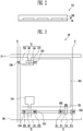
- FIG. 3 is a plan view illustrating a sensor pixel SP in accordance with an exemplary embodiment of the present disclosure.
- a pixel is shown as being coupled to an i-th sensor scan line SSi and a j-th output line Oj (where i is an integer of 2 or more and j is a positive integer).
- the sensor pixel SP may include a sensor electrode 300, a first transistor T1, a second transistor T2, a third transistor T3, and a capacitor electrode 350.
- the first transistor T1 may control a current flowing to the j-th output line Oj.
- the first transistor T1 may be coupled between the j-th output line Oj and the second transistor T2.
- the first transistor T1 may include a first electrode 312 coupled to a second electrode 323 of the second transistor T2, a second electrode 313 coupled to the j-th output line Oj, a gate electrode 314 coupled to the sensor electrode 300, and a semiconductor layer 311 coupled between the first electrode 312 and the second electrode 313.
- the gate electrode 314, the first electrode 312, and the second electrode 313 of the first transistor T1 may be coupled to other components through respective contact holes CHI, CH2, and CH3.
- the first transistor T1 may control a current "lo" which is output to the j-th output line Oj in response to the potential of the sensor electrode 300.
- the second transistor T2 may be coupled between a j-th reference voltage line Pj and the first transistor T1.
- the second transistor T2 may include a first electrode 322 coupled to the j-th reference voltage line Pj, a second electrode 323 coupled to the first electrode 312 of the first transistor T1, a gate electrode 324 coupled to the i-th sensor scan line SSi, and a semiconductor layer 321 coupled between the first electrode 322 and the second electrode 323.
- the first electrode 322 and the second electrode 323 of the second transistor T2 may be coupled to other components through respective contact holes CH4 and CH5.
- the second transistor T2 may be turned on when a sensor scan signal is supplied to the i-th sensor scan line SSi. When the second transistor T2 is turned on, a reference voltage Vcom may be applied to the first electrode 312 of the first transistor T1.
- the third transistor T3 may be coupled between the j-th reference voltage line Pj and the sensor electrode 300.
- the third transistor T3 may include a first electrode 332 coupled to the j-th reference voltage line Pj, a second electrode 333 coupled to the sensor electrode 300, a gate electrode 334 coupled to the i-1-th sensor scan line SSi-1, and a semiconductor layer 331 coupled between the first electrode 332 and the second electrode 333.
- the first electrode 332 and the second electrode 333 of the third transistor T3 may be coupled to other components through respective contact holes CH6 and CH7.
- the third transistor T3 may be turned on when a sensor scan signal is supplied to the i-1-th sensor scan line SSi-1.
- the third transistor T3 When the third transistor T3 is turned on, the voltage of the sensor electrode 300 may be initialized to the reference voltage Vcom.
- the capacitor electrode 350 may be disposed to overlap the sensor electrode 300, and may thus form a capacitor with the sensor electrode 300.
- the capacitor electrode 350 may be coupled to the i-th sensor scan line SSi.
- the capacitor electrode 350 may be coupled to the i-th sensor scan line SSi through the gate electrode 324 of the second transistor T2.
- the capacitor electrode 350 and the gate electrode 324 of the second transistor T2 may be made of the same material as that of the i-th sensor scan line SSi.
- the sensor electrode 300 may form a capacitor with the capacitor electrode 350 and a finger, stylus, or the like, of the user.
- the sensor electrode 300 may include conductive material.
- the conductive material may include a metal material, a metal alloy, a conductive polymer, or a transparent conductive material.
- Examples of the metal material may include copper, silver, gold, platinum, palladium, nickel, tin, aluminum, cobalt, rhodium, iridium, iron, ruthenium, osmium, manganese, molybdenum, tungsten, niobium, tantalum, titanium, bismuth, antimony, and lead.
- examples of the conductive polymer may include polythiophene, polypyrrole, polyaniline, polyacetylene and polyphenylene compounds, and mixtures thereof.
- a poly-3,4-ethylenedioxythiophene/polystyrenesulfonate (PEDOT/PSS) compound of the polythiophene conductive polymer may be used.
- Examples of the transparent conductive material may include silver nanowires (AgNW), indium tin oxide (ITO), indium zinc oxide (IZO), antimony zinc oxide (AZO), indium tin zinc oxide (ITZO), zinc oxide (ZnO), tin oxide (SnO 2 ), a carbon nanotube, and grapheme.
- AgNW silver nanowires
- ITO indium tin oxide
- IZO indium zinc oxide
- AZO antimony zinc oxide
- ITZO indium tin zinc oxide
- ZnO zinc oxide
- SnO 2 tin oxide
- carbon nanotube grapheme
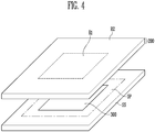
- FIG. 4 is a diagram illustrating in detail a sensor protective layer 200 in accordance with an exemplary embodiment of the present disclosure.
- FIG. 4 illustrates the sensor protective layer 200 which is formed on the sensor pixel SP and the sensor substrate SS.
- the sensor substrate SS and the sensor protective layer 200 are illustrated as being spaced apart from each other as an exploded view. However, the sensor substrate SS and the sensor protective layer 200 may actually be joined together.
- FIG. 4 for the sake of description, only the sensor electrode 300 of the components of the sensor pixel SP shown in FIG. 3 is illustrated, but the present disclosure is not limited thereto.
- the sensor protective layer 200 may include a first region R1, and a second region R2 which extends outwardly from the periphery of the first region R1.
- the first region R1 may be a region disposed over the sensor electrode 300.
- the second region R2 may be a region disposed above a peripheral portion of the sensor electrode 300.
- the sensor protective layer 200 may be relatively hard.
- the sensor protective layer 200 may have a hardness ranging from 8 H to 10 H according to the Mohs hardness system.
- the sensor protective layer 200 may have a relatively high light transmissivity.
- the sensor protective layer 200 may have light transmittance ranging from about 90% to about 100%.
- C refers to capacitance
- E refers to permittivity
- A refers to an area of an electrode plate
- d refers to a distance between electrode plates.
- Er refers to a dielectric constant
- E refers to permittivity
- E0 refers to permittivity in vacuum and has 8.854185 ⁇ 10 ⁇ (-12)F/m (under conditions of room temperature and frequency of 1kHz).
- the permittivity changes depending on the temperature or frequency.
- polycrystalline silicon nitride may have a dielectric constant ranging from 7 to 8 under conditions of room temperature and frequency of 1 MHz.
- barium titanate (BaTiO 3 ) may have a dielectric constant of 1200 or more under conditions of room temperature and frequency of about 1 kHz.
- the first region R1 may have a first permittivity.
- the first permittivity may be a permittivity higher than a second permittivity.
- the first permittivity may be a dielectric constant of 7 or more under conditions of room temperature and frequency of 1 MHz.
- the second region R2 may have the second permittivity different from the first permittivity.
- the second permittivity may be a permittivity lower than the first permittivity.
- the second permittivity may be a dielectric constant which is 1 or more and less than 7 under conditions of room temperature and frequency of 1 MHz.
- the first region R1 may include an inorganic filler at a first ratio.
- the first ratio may be a volume or weight ratio of the inorganic filler to resin that forms the first region R1 of the sensor protective layer 200.
- the first ratio may be set to an appropriate value to give the first region R1 the first permittivity.
- the second region R2 may include an inorganic filler at a second ratio that is lower than the first ratio.
- the second ratio may be a volume or weight ratio of the inorganic filler to resin that forms the second region R2 of the sensor protective layer 200.
- the second ratio may be set to an appropriate value to give the second region R2 the second permittivity.
- the inorganic filler may include at least one of barium titanate (BaTiO 3 ), alumina (Al 2 O 3 ), and titanium dioxide (TiO 2 ).
- barium titanate BaTiO 3
- alumina Al 2 O 3
- titanium dioxide TiO 2
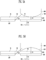
- FIGS. 5A and 5B are sectional diagrams of the sensor pixel SP in accordance with an exemplary embodiment of the present disclosure.
- FIGS. 5A and 5B are diagrams illustrating a change in capacitance of a second capacitor C2 related to the sensor electrode 300 depending on a ridge and a valley of a fingerprint.
- FIG. 5A illustrates the case where a ridge 410 of a finger 400 is disposed over the sensor pixel SP
- FIG. 5B illustrates the case where a valley 420 of the finger 400 is located disposed over the sensor pixel SP.
- the first region R1 of the sensor protective layer 200 may be disposed on the sensor electrode 300.
- the sensor protective layer 200 may be used as a surface to receive a touch of the user.
- an adjacent sensor electrode 300' is also illustrated along with the sensor electrode 300 in FIGS. 5A and 5B .
- the sensor electrode 300 and the capacitor electrode 350 may form a first capacitor C1.
- the sensor electrode 300 and the capacitor electrode 350 may be spaced apart from each other, and at least one insulating layer may be interposed therebetween.
- the sensor electrode 300 and the finger 400 may form a second capacitor C2.
- the second capacitor C2 is a variable capacitor, the capacitance of which may vary depending on whether the ridge 410 or valley 420 of the fingerprint is placed on the sensor electrode 300.
- the capacitance of the second capacitor C2 in the case where the ridge 410 is placed on the sensor electrode 300, as shown in FIG. 5A , and the capacitance of the second capacitor C2 in the case where the valley 420 is placed on the sensor electrode 300, as illustrated in FIG. 5B may differ from each other.
- the read-out circuit 140 may recognize the fingerprint or the palm print of the user by sensing a change in the output current "lo.”
- the sensor electrode 300' and the finger 400 may form a third capacitor C3.
- the third capacitor C3 may be a variable capacitor, and the capacitance of the third capacitor may be undesirable.
- the adjacent sensor electrode 300' might not recognize the ridge 410 or the valley 420 of the finger 400 because of the third capacitor C3. This may cause a defective sensing operation of the fingerprint sensor 100.
- the first region R1 having a relatively high permittivity may be disposed over the sensor electrode 300
- the second region R2 having a relatively low permittivity may be disposed over a region defined between the sensor electrode 300 and the adjacent sensor electrode 300'.
- the capacitance of the second capacitor C2 which may be calculated by Equation 1, may be increased.
- the capacitance of the third capacitor C3, which may be calculated by Equation 1, may be reduced.
- a ratio of the capacitance of the second capacitor C2 to the capacitance of the third capacitor C3 may be comparatively increased.
- the fingerprint sensor 100 in accordance with an exemplary embodiment of the present disclosure, may have enhanced sensing sensitivity.
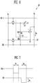
- FIG. 6 is a diagram illustrating an equivalent circuit diagram of the sensor pixel SP shown in FIG. 3 , according to an exemplary embodiment of the present disclosure.
- FIG. 7 is a waveform diagram illustrating the operation of the sensor pixel SP shown in FIG. 6 .
- a sensor pixel SP coupled to an i-th sensor scan line SSi, an i-1-th sensor scan line SSi-1, and a j-th output line Oj is illustrated in FIG. 6 .
- a sensor scan signal that is supplied to the i-1-th sensor scan line SSi-1 and a sensor scan signal that is supplied to the i-th sensor scan line SSi are illustrated.
- the sensor pixel SP may include a sensor electrode 300, a capacitor electrode 350, a first transistor T1, a second transistor T2, and a third transistor T3.
- the sensor electrode 300 and the capacitor electrode 350 may constitute the first capacitor C1.
- the first transistor T1, the second transistor T2, and the third transistor T3 may form a sensor circuit SC.
- the second capacitor C2 which is a variable capacitor, may be formed by the sensor electrode 300 and the finger 400, as described above.
- the capacitance of the second capacitor C2 may change depending on the distance between the sensor electrode 300 and the finger 400, whether the valley or ridge of a fingerprint is placed on the sensor electrode 300, the magnitude of pressure applied by a touch, or the like.
- the first transistor T1 may control a current flowing to the j-th output line Oj.
- the first transistor T1 may be coupled between the j-th output line Oj and the second transistor T2.
- the first transistor T1 may be coupled between the j-th output line Oj and a first node N1, and the gate electrode thereof may be coupled to a second node N2.
- the first transistor T1 may include a first electrode coupled to a second electrode of the second transistor T2, a second electrode coupled to the j-th output line Oj, and a gate electrode coupled to the sensor electrode 300.
- the second transistor T2 may be coupled between a j-th reference voltage line Pj and the first transistor T1.
- the second transistor T2 may be coupled between the j-th reference voltage line Pj and the first node N1, and the gate electrode thereof may be coupled to the i-th sensor scan line SSi.
- the second transistor T2 may include a first electrode coupled to the j-th reference voltage line Pj, a second electrode coupled to the first electrode of the first transistor T1, and a gate electrode coupled to the i-th sensor scan line SSi.
- the second transistor T2 may be turned on when a sensor scan signal is supplied to the i-th sensor scan line SSi.
- a reference voltage Vcom may be applied to the first electrode of the first transistor T1.
- the third transistor T3 may be coupled between the j-th reference voltage line Pj and the sensor electrode 300.
- the third transistor T3 may be coupled between the second node N2 and the j-th reference voltage line Pj, and the gate electrode thereof may be coupled to the i-1-th sensor scan line SSi-1.
- the third transistor T3 may include a first electrode coupled to the j-th reference voltage line Pj, a second electrode coupled to the sensor electrode 300, and a gate electrode coupled to the i-1-th sensor scan line SSi-1.
- the third transistor T3 may be turned on when a sensor scan signal is supplied to the i-1-th sensor scan line SSi-1.
- the third transistor T3 When the third transistor T3 is turned on, the voltage of the sensor electrode 300 may be initialized to the reference voltage Vcom.
- the capacitor electrode 350 may be disposed to overlap the sensor electrode 300, and may thus form the first capacitor C1 with the sensor electrode 300.
- the capacitor electrode 350 may be coupled to the i-th sensor scan line SSi.
- the first capacitor C1 may be coupled between the second node N1 and the i-th sensor scan line SSi.
- the second capacitor C2 may be coupled to the second node N2.
- the first node N1 is a node to which the first electrode of the first transistor T1 and the second electrode of the second transistor T2 are coupled in common
- the second node N2 is a node to which the sensor electrode 300, the gate electrode of the first transistor T1, and the second electrode of the third transistor T3 are coupled in common.
- the first electrode of each of the transistors T1, T2, and T3 may be set to any one of a source electrode and a drain electrode, and the second electrode of each of the transistors T1, T2, and T3 may be set to an electrode different from the first electrode. For example, if the first electrode is set to a source electrode, the second electrode may be set to a drain electrode.
- FIG. 6 illustrates an example in which the transistors T1, T2, and T3 are PMOS transistors, but in various embodiments, the transistors T1, T2, and T3 may be embodied by NMOS transistors.
- FIG. 7 is a waveform diagram illustrating the operation of the sensor pixel SP shown in FIG. 6 .
- a sensor scan signal may be supplied to the i-1-th sensor scan line SSi-1.
- the third transistor T3 may remain turned on, and the second node N2 may be initialized to the reference voltage Vcom which is applied from the j-th reference voltage line Pj.
- the sensor scan signal may be supplied to the i-th sensor scan line SSi.
- the second transistor T2 may remain turned on, and the current "Io" may flow from the j-th reference voltage line Pj to the j-th output line Oj through the second transistor T2 and the first transistor T1.
- the first transistor T1 may control the amount of output current "Io" in response to a gate voltage (e.g., voltage applied to the second node N2).
- a gate voltage e.g., voltage applied to the second node N2.
- Vcom denotes the reference voltage
- Vc1 denotes the capacitance of the first capacitor C1
- Vc2 denotes the capacitance of the second capacitor C2
- Vs denotes a change in the voltage of the sensor scan signal that is supplied to the i-th sensor scan line SSi.
- FIGS. 8A to 8E are diagrams illustrating a method of manufacturing the fingerprint sensor in accordance with an exemplary embodiment of the present disclosure.
- FIGS. 8A to 8E for the sake of description, only the sensor electrode 300 of the components of the sensor pixel SP shown in FIG. 3 is illustrated, but the present disclosure is not limited thereto.
- a plurality of sensor pixels SP may be formed on the sensor substrate SS.
- Each of the sensor pixels SP may include the sensor electrode 300.
- a mask MK including openings BK may be disposed over the plurality of sensor pixels SP.
- the openings BK are holes in the mask MK.
- the mask MK may be aligned over the plurality of sensor pixels SP such that the openings BK are disposed over the respective sensor electrodes included in the sensor pixels SP.
- first resin RS1 may be applied on the sensor electrodes 300 through the openings BK of the mask MK.
- the first resin RS1 may have a first permittivity.
- the first permittivity may be a permittivity higher than a second permittivity.
- the first permittivity may be a dielectric constant of 7 or more under conditions of room temperature and frequency of 1 MHz.
- the mask MK may be removed, and an upper surface of the sensor substrate SS may be planarized using second resin RS2.
- the second resin RS2 may be formed on a portion of the sensor substrate SS on which the first resin RS1 has not been formed.
- the upper surface of the first resin RS1 may be level with that of the second resin RS2.
- the second resin RS2 may have a second permittivity different from the first permittivity.
- the second permittivity may be a permittivity lower than the first permittivity.
- the second permittivity may be a dielectric constant which is 1 or more and less than 7 under conditions of room temperature and frequency of 1 MHz.
- the first resin RS1 and the second resin RS2 may be hardened, for example, within a single hardening step.
- the first resin RS1 and the second resin RS2 may be hardened by an optical (using light) or thermal (using heat) hardening method.
- a sensor protective layer 200 may be formed on the plurality of sensor pixels SP and the sensor substrate SS.
- the sensor protective layer 200 may include a first region R1 in which the first resin RS1 has been hardened, and a second region R2 in which the second resin RS2 has been hardened.
- the sensor protective layer 200 may be relatively hard.
- the sensor protective layer 20 may have a hardness ranging from 8 H to 10 H.
- the sensor protective layer 200 may be transmissive of light.
- the sensor protective layer 200 may have light transmittance ranging from 90% to 100%.
- the first region R1 may have a first permittivity.
- the first permittivity may be a permittivity higher than a second permittivity.
- the first permittivity may be a dielectric constant of 7 or more under conditions of room temperature and frequency of 1 MHz.
- the second region R2 may have the second permittivity different from the first permittivity.
- the second permittivity may be a permittivity lower than the first permittivity.
- the second permittivity may be a dielectric constant which is 1 or more and less than 7 under conditions of room temperature and frequency of 1 MHz.
- the first region R1 may include an inorganic filler at a first ratio.
- the first ratio may be a volume or weight ratio of the inorganic filler to resin that forms the first region R1 of the sensor protective layer 200.
- the first ratio may be set to an appropriate value to give the first region R1 the first permittivity.
- the second region R2 may include an inorganic filler at a second ratio that is lower than the first ratio.
- the second ratio may be a volume or weight ratio of the inorganic filler to resin that forms the second region R2 of the sensor protective layer 200.
- the second ratio may be set to an appropriate value to give the second region R2 the second permittivity.
- the inorganic filler may include at least one of barium titanate (BaTiO 3 ), alumina (Al 2 O 3 ), and titanium dioxide (TiO 2 ).
- barium titanate BaTiO 3
- alumina Al 2 O 3
- titanium dioxide TiO 2
- FIGS. 9A to 9E are diagrams illustrating a method of manufacturing the fingerprint sensor in accordance with an exemplary embodiment of the present disclosure.
- FIGS. 9A to 9E for the sake of description, only the sensor electrode 300 of the components of the sensor pixel SP shown in FIG. 3 is illustrated, but the present disclosure is not limited thereto.
- a plurality of sensor pixels SP may be formed on the sensor substrate SS.
- Each of the sensor pixels SP may include the sensor electrode 300.
- a sensor protective layer 200 may be applied on the sensor substrate SS and the sensor pixels SP.
- the same reference numeral is used to designate the sensor protective layer 200 shown in FIGS. 9B to 9E .
- the sensor protective layer 200 shown in FIGS. 9B and 9C may differ from the sensor protective layer 200 shown in FIGS. 9D and 9E in terms of permittivity or a distribution ratio of inorganic filler. Details pertaining to this will be described below.
- the sensor protective layer 200 shown in FIG. 9B may have a reference permittivity.
- the reference permittivity may be a median permittivity which is lower than a first permittivity and higher than a second permittivity.
- the sensor protective layer 200 may include an inorganic filler at a reference ratio.
- the reference ratio may be a volume or weight ratio of the inorganic filler to resin that forms the sensor protective layer 200.
- the reference ratio may be set to an appropriate value to give the sensor protective layer 200 the reference permittivity.
- a mask MK including openings BK may be disposed over the sensor protective layer 200.
- the mask MK may be aligned over the plurality of sensor pixels SP such that the openings BK are disposed over the respective sensor electrodes included in the sensor pixels SP.
- light IL may be incident through the openings.
- the light IL may be incident on only the sensor electrodes 300 included in the sensor pixels SP by the mask MK.
- the light IL may be applied to the sensor protective layer 200 through the openings BK.
- the light IL may be ultraviolet light.
- the inorganic filler included in the sensor protective layer 200 may be concentrated into the first regions R1 to which the light IL is applied. Photoreaction material contained in the inorganic filler may react to the light IL, thus making the inorganic filler concentrated into the first regions R1.
- the inorganic filler may be a component having a permittivity higher than the reference permittivity.
- the first region R1 disposed on each sensor electrode 300 may have the first permittivity
- the second region R2 disposed on the peripheral portion of the sensor electrode 300 may have the second permittivity
- the first region R1 may have the first permittivity.
- the first permittivity may be a permittivity higher than the second permittivity.
- the first permittivity may be a dielectric constant of 7 or more under conditions of room temperature and frequency of 1 MHz.
- the second region R2 may have the second permittivity different from the first permittivity.
- the second permittivity may be a permittivity lower than the first permittivity.
- the second permittivity may be a dielectric constant which is 1 or more and less than 7 under conditions of room temperature and frequency of 1 MHz.
- the first region R1 may include an inorganic filler at a first ratio.
- the first ratio may be a volume or weight ratio of the inorganic filler to resin that forms the first region R1 of the sensor protective layer 200.
- the first ratio may be set to an appropriate value to give the first region R1 the first permittivity.
- the second region R2 may include the inorganic filler at a second ratio that is lower than the first ratio.
- the second ratio may be a volume or weight ratio of the inorganic filler to resin that forms the second region R2 of the sensor protective layer 200.
- the second ratio may be set to an appropriate value to give the second region R2 the second permittivity.
- the inorganic filler may include at least one of barium titanate (BaTiO 3 ), alumina (Al 2 O 3 ), and titanium dioxide (TiO 2 ).
- barium titanate BaTiO 3
- alumina Al 2 O 3
- titanium dioxide TiO 2
- the mask MK may be removed.
- the sensor protective layer 200 may be hardened.
- the sensor protective layer 200 may be hardened by an optical (by light) or thermal (by heat) hardening method.
- the sensor protective layer 200 may be relatively hard.
- the sensor protective layer 20 may have a hardness ranging from 8 H to 10 H.
- the sensor protective layer 200 may be transmissive of light.
- the sensor protective layer 200 may have light transmittance ranging from 90% to 100%.
- FIG. 10 is a flowchart of the fingerprint sensor manufacturing method shown in FIGS. 8A to 8E .
- the sensor pixels SP may be formed on the sensor substrate SS, at step S110.
- Each of the sensor pixels SP may include the sensor electrode 300.
- the mask MK including the openings BK may be disposed over the sensor pixels SP, at step S120.
- the mask MK may be aligned over the plurality of sensor pixels SP such that the openings BK are disposed over the respective sensor electrodes included in the sensor pixels SP.
- the first resin RS1 may be applied on the sensor electrodes 300 through the openings BK of the mask MK, at step S130. Therefore, the first resin RS1 may be formed on only the sensor electrodes 300.
- the mask MK may be removed, at step S140.
- the upper surface of the sensor substrate SS may be planarized using the second resin RS2, at step S150.
- the second resin RS2 may be formed on a portion of the sensor substrate SS on which the first resin RS1 has not been formed. After the planarization, the upper surface of the first resin RS1 may be level with that of the second resin RS2.
- the first resin RS1 and the second resin RS2 may be hardened, at step S160.
- the first resin RS1 and the second resin RS2 may be hardened by an optical or thermal hardening method.
- the sensor protective layer 200 may be formed on the sensor pixels SP and the sensor substrate SS.
- the sensor protective layer 200 may include the first region R1, in which the first resin RS1 has been hardened, and the second region R2, in which the second resin RS2 has been hardened.
- FIG. 11 is a flowchart of the fingerprint sensor manufacturing method shown in FIGS. 9A to 9E .
- the sensor pixels SP may be formed on the sensor substrate SS, at step S210.
- Each of the sensor pixels SP may include the sensor electrode 300.
- the sensor protective layer 200 may be applied on the sensor substrate SS and the sensor pixels SP, at step S220.
- the sensor protective layer 200 may include an inorganic filler at a reference ratio.
- the sensor protective layer 200 may include at least one of barium titanate (BaTiO 3 ), alumina (Al 2 O 3 ), and titanium dioxide (TiO 2 ).
- the mask MK including the openings BK may be disposed over the sensor protective layer 200, at step S230.
- the mask MK may be aligned over the plurality of sensor pixels SP such that the openings BK are disposed over the respective sensor electrodes included in the sensor pixels SP.
- Light IL may be incident through the openings BK, at step S240.
- the light IL may be incident on only the sensor electrodes 300 included in the sensor pixels SP by the mask MK.
- the light IL may be applied to the sensor protective layer 200 through the openings BK.
- the light IL may be ultraviolet light.
- the inorganic filler e.g., barium titanate
- the inorganic filler included in the sensor protective layer 200 may be concentrated into portions (e.g., first regions R1) to which the light IL is applied.
- photoreaction material contained in the inorganic filler may react to the light IL, thus making the inorganic filler concentrated into the first regions R1.
- the inorganic filler may be a component having a permittivity higher than the reference permittivity.
- the first region R1 disposed on each sensor electrode 300 may have the first permittivity
- the second region R2 disposed on the peripheral portion of the sensor electrode 300 may have the second permittivity
- the mask MK may be removed, at step S250.
- the sensor protective layer 200 may be hardened, at step S260.
- the sensor protective layer 200 may be hardened by an optical (with light) or thermal (with heat) hardening method.
- a fingerprint sensor in accordance with an exemplary embodiment of the present disclosure, may satisfy a required window sensing distance condition and have increased sensing sensitivity.
- the fingerprint sensor in accordance with an exemplary embodiment of the present disclosure, may have enhanced hardness.
- a method of manufacturing a fingerprint sensor in accordance with an exemplary embodiment of the present disclosure may simplify a manufacturing process.
Landscapes
- Engineering & Computer Science (AREA)
- Theoretical Computer Science (AREA)
- General Engineering & Computer Science (AREA)
- Human Computer Interaction (AREA)
- Physics & Mathematics (AREA)
- General Physics & Mathematics (AREA)
- Multimedia (AREA)
- Measurement Of Length, Angles, Or The Like Using Electric Or Magnetic Means (AREA)
- Image Input (AREA)
Abstract
Description
- The present disclosure relates to a fingerprint sensor, and more particularly, to a fingerprint sensor and a method of manufacturing the same.
- Fingerprint sensors have been incorporated into a surface of a display device.
- One example of such an apparatus is an active self-capacitive fingerprint sensor. The active self-capacitive fingerprint sensor senses a fingerprint based on a change in capacitance of a capacitor formed between it and the hand of a user.
- In the active self-capacitive fingerprint sensor, the minimum distance required between a sensor electrode of the fingerprint sensor and the hand of the user is larger than is typical for mutual-capacitive fingerprint sensors. This distance is known as the "window sensing distance."
- A fingerprint sensor includes a sensor substrate. A plurality of sensor pixels is configured to sense a change in capacitance corresponding to a touch of a user. Each of the plurality of sensor pixels includes a sensor electrode. A sensor protective layer is configured to protect the sensor substrate and the plurality of sensor pixels. The sensor protective layer includes a first region disposed over the sensor electrode, and a second region. The first region has a first permittivity. The second region has a second permittivity lower than the first permittivity. Preferably, the sensor protective layer has a hardness ranging from 8 H to 10 H. Preferably, the fingerprint sensor further comprises a plurality of sensor scan lines coupled with the plurality of sensor pixels and a plurality of output lines coupled with the plurality of sensor pixels, wherein a sensor pixel, of the plurality of sensor pixels, coupled with an i-th sensor scan line, where i is an integer of 2 or more, and a j-th output line, where j is a positive integer, comprises: a first transistor comprising a first gate electrode coupled to the sensor electrode, the first transistor being configured to control current to be outputted through the j-th output line; a second transistor comprising a second gate electrode coupled to the i-th sensor scan line, the second transistor being coupled between a reference voltage line and the first transistor; and a capacitor electrode configured to form a first capacitor with the sensor electrode, and coupled to the i-th sensor scan line. Preferably, the sensor pixel further comprises a third transistor comprising a third gate electrode coupled to an (i-1)-th scan line, the third transistor being coupled between the reference voltage line and the sensor electrode. Preferably, when a touch is generated, the plurality of sensor electrodes form a second capacitor with a hand of a user. Preferably, the fingerprint sensor is configured to recognize a fingerprint or a palm print of the user using a change in a capacitance of the second capacitor corresponding to the touch. Preferably, the fingerprint sensor further comprises: a sensor scan driver configured to sequentially supply sensor scan signals to the sensor scan lines. Preferably, the fingerprint sensor further comprises: a read-out circuit configured to detect a fingerprint or a palm print using current output from through the output lines. Preferably, the sensor protective layer has a light transmittance ranging from 90% to 100%. Preferably, the first region includes an inorganic filler at a first ratio, and the second region includes the inorganic filler at a second ratio that is lower than the first ratio. Preferably, the inorganic filler includes barium titanate, alumina, or titanium dioxide. Preferably, the fingerprint sensor further comprises a plurality of display pixels configured to display an image. Preferably, the sensor protective layer has a hardness ranging from 8 H to 10 H.
- A method of manufacturing a fingerprint sensor includes forming a plurality of sensor pixels on a sensor substrate. Each of the plurality of sensor pixels includes a sensor electrode. A mask is disposed over the sensor substrate and the plurality of sensor pixels. The mask includes a plurality of openings. A first resin is applied on the sensor electrodes through the plurality of openings. The sensor substrate is planarized by disposing a second resin. A sensor protective layer is formed by hardening the first resin and the second resin. The first resin has a first permittivity, and the second resin has a second permittivity lower than the first permittivity. Preferably, the sensor protective layer has a hardness ranging from 8 H to 10 H. Preferably, the first resin includes an inorganic filler at a first ratio, and the second resin includes the inorganic filler at a second ratio that is lower than the first ratio. Preferably, the inorganic filler includes barium titanate, alumina, or titanium dioxide. Preferably, the disposing of the mask over the sensor substrate and the plurality of sensor pixels comprises: aligning the mask over the sensor substrate and the plurality of sensor pixels such that the plurality of openings are disposed over respective sensor electrodes of the plurality of sensor electrodes. Preferably, the first resin and the second resin are hardened by an optical or thermal hardening method.
- A method of manufacturing a fingerprint sensor includes forming a plurality of sensor pixels on a sensor substrate. Each of the plurality of sensor pixels includes a sensor electrode. A sensor protective layer is applied on the sensor substrate and the plurality of sensor pixels. A mask is disposed over the sensor protective layer. The mask includes a plurality of openings. Light is applied to the sensor protective layer through the plurality of openings. The sensor protective layer is hardened. After the hardening of the sensor protective layer, the sensor protective layer includes a first region formed over and aligned with the sensor electrode, and a second region formed over and aligned with a peripheral portion of the sensor electrode. The first region has a first permittivity, and the second region has a second permittivity lower than the first permittivity. Preferably, the first region includes an inorganic filler at a first ratio, and the second region includes the inorganic filler at a second ratio that is lower than the first ratio. Preferably, the inorganic filler includes barium titanate, alumina, or titanium dioxide.
- A more complete appreciation of the present disclosure and many of the attendant aspects thereof will be readily obtained as the same becomes better understood by reference to the following detailed description when considered in connection with the accompanying drawings, wherein:
-
FIG. 1 is a diagram illustrating a fingerprint sensor in accordance with an exemplary embodiment of the present disclosure; -
FIG. 2 is a partial sectional diagram illustrating the fingerprint sensor in accordance with an exemplary embodiment of the present disclosure; -
FIG. 3 is a plan diagram illustrating a sensor pixel in accordance with an exemplary embodiment of the present disclosure; -
FIG. 4 is a diagram illustrating a sensor protective layer in accordance with an exemplary embodiment of the present disclosure; -
FIGS. 5A and 5B are diagrams illustrating a change in capacitance of a second capacitor related to a sensor electrode depending on a ridge and a valley of a fingerprint in accordance with exemplary embodiments of the present disclosure; -
FIG. 6 is a diagram illustrating an equivalent circuit of the sensor pixel shown inFIG. 3 , according to an exemplary embodiment of the present invention; -
FIG. 7 is a waveform diagram illustrating the operation of the sensor pixel shown inFIG. 6 ; -
FIGS. 8A to 8E are diagrams illustrating a method of manufacturing the fingerprint sensor in accordance with an exemplary embodiment of the present disclosure; -
FIGS. 9A to 9E are diagrams illustrating a method of manufacturing the fingerprint sensor in accordance with an exemplary embodiment of the present disclosure; -
FIG. 10 is a flowchart illustrating the fingerprint sensor manufacturing method shown inFIGS. 8A to 8E ; and -
FIG. 11 is a flowchart illustrating the fingerprint sensor manufacturing method shown inFIGS. 9A to 9E . - Reference will now be made in detail to various exemplary embodiments of the present disclosure, specific examples of which are illustrated in the accompanying drawings and described below, since the embodiments of the present disclosure can be variously modified in many different forms. However, it is to be appreciated that all changes, equivalents, and substitutes do not depart from the technical scope of the present disclosure and are encompassed in the present disclosure.
- It will be understood that, although the terms "first", "second", etc. may be used herein to describe various components, these components should not be limited by these terms. These terms are only used to distinguish one component from other components.
- The drawings are not necessarily drawn to scale and in some instances, proportions may be exaggerated in order to clearly illustrate features of the embodiments. Like reference numerals may refer to like elements throughout the specification and figures. For example, when a first layer is referred to as being "on" a second layer or "on" a substrate, it not only refers to a case where the first layer is formed directly on the second layer or the substrate but also a case where a third layer exists between the first layer and the second layer or the substrate. Hereinafter, exemplary embodiments of the present disclosure will be described in detail with reference to the attached drawings.
-
FIG. 1 is a diagram illustrating afingerprint sensor 100 in accordance with an exemplary embodiment of the present disclosure.FIG. 2 is a partial sectional diagram illustrating thefingerprint sensor 100 shown inFIG. 1 . - The
fingerprint sensor 100, in accordance with an exemplary embodiment of the present disclosure, may recognize a touch of a user. - Referring to
FIGS. 1 and2 , thefingerprint sensor 100, in accordance with an exemplary embodiment of the present disclosure, may include asensor unit 110. - The
sensor unit 110 may include a sensor substrate SS, a plurality of sensor pixels SP, and a sensorprotective layer 200. - The sensor substrate SS may include an insulating material such as glass or resin. Furthermore, the sensor substrate SS may be flexible, bendable, and/or foldable, and may have a single-layer structure or multi-layer structure.
- For example, the sensor substrate SS may include polystyrene, polyvinyl alcohol, polymethyl methacrylate, polyethersulfone, polyacrylate, polyetherimide, polyethylene naphthalate, polyethylene terephthalate, polyphenylene sulfide, polyarylate, polyimide, polycarbonate, triacetate cellulose, and/or cellulose acetate propionate.
- The material constituting the sensor substrate SS may be changed in various ways, for example, the sensor substrate SS may include glass fiber reinforced plastic (FRP) or the like.
- The sensor pixels SP may be disposed on the sensor substrate SS. The sensor pixels SP may be coupled with sensor scan lines SS0 to SSn and output lines O1 to Om. For example, the sensor pixels SP may be arranged in the form of a matrix at intersections of reference voltage lines P1 to Pm and the sensor scan lines SS0 to SSn.
- The sensor pixels SP may each receive sensor scan signals through the sensor scan lines SS0 to SSn. The sensor pixels SP may output predetermined current corresponding to a touch state to the associated output lines O1 to Om during a supply period of the sensor scan signal.
- The sensor scan lines SS0 to SSn may be disposed on the sensor substrate SS, may extend predetermined lengths in a first direction (e.g., an X-axis direction), and may be coupled to the sensor pixels SP on a line basis.
- The output lines O1 to Om may be disposed on the sensor substrate SS, may extend predetermined lengths in a second direction (e.g., a Y-axis direction), and may be coupled to the sensor pixels SP on a line basis.
- The sensor pixels SP may be coupled to the reference voltage lines P1 to Pm, and may be supplied with a reference voltage Vcom through the reference voltage lines P1 to Pm.
- The reference voltage lines P1 to Pm may extend predetermined lengths in the second direction (e.g., the Y-axis direction), and may be coupled to the sensor pixels SP on a line basis.
- For example, the reference voltage lines P1 to Pm may be arranged in parallel to the output lines O1 to Om.
- The arrangement direction of the reference voltage lines P1 to Pm may be changed in various forms, and the reference voltage lines P1 to Pm may be arranged in parallel to, for example, the sensor scan lines SS0 to SSn.
- The reference voltage lines P1 to Pm may be electrically coupled to each other to maintain the same electrical potential at each voltage line. For example, the reference voltage lines P1 to Pm may be electrically coupled to each other in the perimeter of the sensor substrate SS via a line Pa.
- The sensor
protective layer 200 may protect the sensor substrate SS and the sensor pixels SP and may be formed on both the sensor substrate SS and the sensor pixels SP. - The sensor
protective layer 200 may form a surface to receive the touch of the user, and may have a single-layer structure or multi-layer structure. - For example, the sensor
protective layer 200 may be made of insulating material such as glass or resin. The sensorprotective layer 200 may be flexible, bendable, and/or foldable. For example, the sensorprotective layer 200 may include one or more materials capable of constituting the sensor substrate SS. - Details related to the sensor
protective layer 200 will be described with reference toFIG. 4 . - The
fingerprint sensor 100, in accordance with an exemplary embodiment of the present disclosure, may further include asensor driving unit 120. - The
sensor driving unit 120 may include asensor scan driver 130 for driving thefingerprint sensor 100, a read-out circuit 140, and apower supply unit 150. - The
sensor scan driver 130 may supply sensor scan signals to the sensor pixels SP through the sensor scan lines SS0 to SSn. For example, thesensor scan driver 130 may sequentially output the sensor scan signals to the sensor scan lines SS0 to SSn. - The sensor scan signals may have voltage levels sufficient to turn on transistors associated therewith.
- For connection with the sensor scan lines SSo to SSn, the
sensor scan driver 130 may be directly mounted on the sensor substrate SS or may be coupled to the sensor substrate SS through a separate component such as a flexible printed circuit board (FPCB). - The read-
out circuit 140 may receive signals (e.g., currents), output from the sensor pixels SP, through the output lines O1 to Om. - For example, when the
sensor scan driver 130 sequentially supplies the sensor scan signals, the sensor pixels SP may be selected on a line basis, and the read-out circuit 140 may sequentially receive, through the output lines O1 to Om, current output from the sensor pixels SP selected on a line basis. - Here, the read-
out circuit 140 may recognize a touch by sensing a change in current. - For example, the touch information may include the location of a touch detected by the
fingerprint sensor 100, and valleys and ridges of a fingerprint or palm print. - For connection with the output lines O1 to Om, the read-
out circuit 140 may be directly mounted on the sensor substrate SS, or may be coupled with the sensor substrate SS by a separate component such as a flexible printed circuit board. - The
power supply unit 150 may supply a reference voltage Vcom to the sensor pixels SP through the reference voltage lines P1 to Pm. - For connection with the reference voltage lines P1 to Pm, the
power supply unit 150 may be directly mounted on the sensor substrate SS, or may be coupled with the sensor substrate SS by a separate component such as a flexible printed circuit board. - In
FIG. 1 , an example in which thesensor scan driver 130, the read-out circuit 140, and thepower supply unit 150 are separately provided is illustrated, however, at least some of the foregoing components may be integrated with each other where desired. - The
sensor scan driver 130, the read-out circuit 140, and thepower supply unit 150 may each be installed using any one of various methods, such as chip on glass, chip on plastic, tape carrier package, and chip on film methods. -
FIG. 3 is a plan view illustrating a sensor pixel SP in accordance with an exemplary embodiment of the present disclosure. InFIG. 3 a pixel is shown as being coupled to an i-th sensor scan line SSi and a j-th output line Oj (where i is an integer of 2 or more and j is a positive integer). - Referring to
FIG. 3 , the sensor pixel SP, in accordance with an exemplary embodiment of the present disclosure, may include asensor electrode 300, a first transistor T1, a second transistor T2, a third transistor T3, and acapacitor electrode 350. - The first transistor T1 may control a current flowing to the j-th output line Oj. For this operation, the first transistor T1 may be coupled between the j-th output line Oj and the second transistor T2.
- For example, the first transistor T1 may include a
first electrode 312 coupled to asecond electrode 323 of the second transistor T2, asecond electrode 313 coupled to the j-th output line Oj, agate electrode 314 coupled to thesensor electrode 300, and asemiconductor layer 311 coupled between thefirst electrode 312 and thesecond electrode 313. - The
gate electrode 314, thefirst electrode 312, and thesecond electrode 313 of the first transistor T1 may be coupled to other components through respective contact holes CHI, CH2, and CH3. - Therefore, the first transistor T1 may control a current "lo" which is output to the j-th output line Oj in response to the potential of the
sensor electrode 300. - The second transistor T2 may be coupled between a j-th reference voltage line Pj and the first transistor T1.
- For example, the second transistor T2 may include a
first electrode 322 coupled to the j-th reference voltage line Pj, asecond electrode 323 coupled to thefirst electrode 312 of the first transistor T1, agate electrode 324 coupled to the i-th sensor scan line SSi, and asemiconductor layer 321 coupled between thefirst electrode 322 and thesecond electrode 323. - The
first electrode 322 and thesecond electrode 323 of the second transistor T2 may be coupled to other components through respective contact holes CH4 and CH5. - The second transistor T2 may be turned on when a sensor scan signal is supplied to the i-th sensor scan line SSi. When the second transistor T2 is turned on, a reference voltage Vcom may be applied to the
first electrode 312 of the first transistor T1. - The third transistor T3 may be coupled between the j-th reference voltage line Pj and the
sensor electrode 300. - For example, the third transistor T3 may include a
first electrode 332 coupled to the j-th reference voltage line Pj, asecond electrode 333 coupled to thesensor electrode 300, agate electrode 334 coupled to the i-1-th sensor scan line SSi-1, and asemiconductor layer 331 coupled between thefirst electrode 332 and thesecond electrode 333. - The
first electrode 332 and thesecond electrode 333 of the third transistor T3 may be coupled to other components through respective contact holes CH6 and CH7. - The third transistor T3 may be turned on when a sensor scan signal is supplied to the i-1-th sensor scan line SSi-1. When the third transistor T3 is turned on, the voltage of the
sensor electrode 300 may be initialized to the reference voltage Vcom. - The
capacitor electrode 350 may be disposed to overlap thesensor electrode 300, and may thus form a capacitor with thesensor electrode 300. - The
capacitor electrode 350 may be coupled to the i-th sensor scan line SSi. For example, thecapacitor electrode 350 may be coupled to the i-th sensor scan line SSi through thegate electrode 324 of the second transistor T2. - Here, the
capacitor electrode 350 and thegate electrode 324 of the second transistor T2 may be made of the same material as that of the i-th sensor scan line SSi. - The
sensor electrode 300 may form a capacitor with thecapacitor electrode 350 and a finger, stylus, or the like, of the user. - The
sensor electrode 300 may include conductive material. For example, the conductive material may include a metal material, a metal alloy, a conductive polymer, or a transparent conductive material. - Examples of the metal material may include copper, silver, gold, platinum, palladium, nickel, tin, aluminum, cobalt, rhodium, iridium, iron, ruthenium, osmium, manganese, molybdenum, tungsten, niobium, tantalum, titanium, bismuth, antimony, and lead.
- Furthermore, examples of the conductive polymer may include polythiophene, polypyrrole, polyaniline, polyacetylene and polyphenylene compounds, and mixtures thereof. In particular, a poly-3,4-ethylenedioxythiophene/polystyrenesulfonate (PEDOT/PSS) compound of the polythiophene conductive polymer may be used.
- Examples of the transparent conductive material may include silver nanowires (AgNW), indium tin oxide (ITO), indium zinc oxide (IZO), antimony zinc oxide (AZO), indium tin zinc oxide (ITZO), zinc oxide (ZnO), tin oxide (SnO2), a carbon nanotube, and grapheme.
-
FIG. 4 is a diagram illustrating in detail a sensorprotective layer 200 in accordance with an exemplary embodiment of the present disclosure.FIG. 4 illustrates the sensorprotective layer 200 which is formed on the sensor pixel SP and the sensor substrate SS. InFIG. 4 , for the sake of description, the sensor substrate SS and the sensorprotective layer 200 are illustrated as being spaced apart from each other as an exploded view. However, the sensor substrate SS and the sensorprotective layer 200 may actually be joined together. Furthermore, inFIG. 4 , for the sake of description, only thesensor electrode 300 of the components of the sensor pixel SP shown inFIG. 3 is illustrated, but the present disclosure is not limited thereto. - Referring to
FIGS. 2 to 4 , the sensorprotective layer 200 may include a first region R1, and a second region R2 which extends outwardly from the periphery of the first region R1. - The first region R1 may be a region disposed over the
sensor electrode 300. The second region R2 may be a region disposed above a peripheral portion of thesensor electrode 300. - The sensor
protective layer 200 may be relatively hard. For example, the sensorprotective layer 200 may have a hardness ranging from 8 H to 10 H according to the Mohs hardness system. - The sensor
protective layer 200 may have a relatively high light transmissivity. For example, the sensorprotective layer 200 may have light transmittance ranging from about 90% to about 100%. - Hereinbelow, permittivity of the sensor
protective layer 200 will be described.
- Here, C refers to capacitance, E refers to permittivity, A refers to an area of an electrode plate, and d refers to a distance between electrode plates.

- Here, Er refers to a dielectric constant, E refers to permittivity, and E0 refers to permittivity in vacuum and has 8.854185×10^(-12)F/m (under conditions of room temperature and frequency of 1kHz).
- In detail, the permittivity changes depending on the temperature or frequency.
- For example, polycrystalline silicon nitride may have a dielectric constant ranging from 7 to 8 under conditions of room temperature and frequency of 1 MHz.
- For example, barium titanate (BaTiO3) may have a dielectric constant of 1200 or more under conditions of room temperature and frequency of about 1 kHz.
- The first region R1 may have a first permittivity. The first permittivity may be a permittivity higher than a second permittivity. For example, the first permittivity may be a dielectric constant of 7 or more under conditions of room temperature and frequency of 1 MHz.
- The second region R2 may have the second permittivity different from the first permittivity. The second permittivity may be a permittivity lower than the first permittivity. For example, the second permittivity may be a dielectric constant which is 1 or more and less than 7 under conditions of room temperature and frequency of 1 MHz.
- The first region R1 may include an inorganic filler at a first ratio. The first ratio may be a volume or weight ratio of the inorganic filler to resin that forms the first region R1 of the sensor
protective layer 200. The first ratio may be set to an appropriate value to give the first region R1 the first permittivity. - The second region R2 may include an inorganic filler at a second ratio that is lower than the first ratio. The second ratio may be a volume or weight ratio of the inorganic filler to resin that forms the second region R2 of the sensor
protective layer 200. The second ratio may be set to an appropriate value to give the second region R2 the second permittivity. - For example, the inorganic filler may include at least one of barium titanate (BaTiO3), alumina (Al2O3), and titanium dioxide (TiO2).
-
FIGS. 5A and 5B are sectional diagrams of the sensor pixel SP in accordance with an exemplary embodiment of the present disclosure.FIGS. 5A and 5B are diagrams illustrating a change in capacitance of a second capacitor C2 related to thesensor electrode 300 depending on a ridge and a valley of a fingerprint. - For example,
FIG. 5A illustrates the case where aridge 410 of afinger 400 is disposed over the sensor pixel SP, andFIG. 5B illustrates the case where avalley 420 of thefinger 400 is located disposed over the sensor pixel SP. - Referring to
FIGS. 4 to 5A and5B , the first region R1 of the sensorprotective layer 200 may be disposed on thesensor electrode 300. The sensorprotective layer 200 may be used as a surface to receive a touch of the user. - For the sake of description, an adjacent sensor electrode 300' is also illustrated along with the
sensor electrode 300 inFIGS. 5A and 5B . - The
sensor electrode 300 and thecapacitor electrode 350 may form a first capacitor C1. Thesensor electrode 300 and thecapacitor electrode 350 may be spaced apart from each other, and at least one insulating layer may be interposed therebetween. - When the
finger 400 of the user is placed on the sensor pixel SP to recognize a fingerprint, thesensor electrode 300 and thefinger 400 may form a second capacitor C2. - Here, the second capacitor C2 is a variable capacitor, the capacitance of which may vary depending on whether the
ridge 410 orvalley 420 of the fingerprint is placed on thesensor electrode 300. - Since the distance between the
ridge 410 and thesensor electrode 300 is shorter than the distance between thevalley 420 and thesensor electrode 300, the capacitance of the second capacitor C2 in the case where theridge 410 is placed on thesensor electrode 300, as shown inFIG. 5A , and the capacitance of the second capacitor C2 in the case where thevalley 420 is placed on thesensor electrode 300, as illustrated inFIG. 5B , may differ from each other. - Referring to
FIGS. 1 to 5A and5B , since a change in the capacitance of the second capacitor C2 influences the output current "lo" of the sensor pixel SP, the read-out circuit 140 may recognize the fingerprint or the palm print of the user by sensing a change in the output current "lo." - The sensor electrode 300' and the
finger 400 may form a third capacitor C3. The third capacitor C3 may be a variable capacitor, and the capacitance of the third capacitor may be undesirable. - As shown in
FIGS. 5A and 5B , the adjacent sensor electrode 300' might not recognize theridge 410 or thevalley 420 of thefinger 400 because of the third capacitor C3. This may cause a defective sensing operation of thefingerprint sensor 100. - To avoid the above-mentioned problem, in the
fingerprint sensor 100, in accordance with an exemplary embodiment of the present disclosure, the first region R1, having a relatively high permittivity, may be disposed over thesensor electrode 300, and the second region R2, having a relatively low permittivity, may be disposed over a region defined between thesensor electrode 300 and the adjacent sensor electrode 300'. - As shown in
FIGS. 5A and 5B , when the first region R1 having a high permittivity is disposed between thesensor electrode 300 and theridge 410 or thevalley 420, the capacitance of the second capacitor C2, which may be calculated byEquation 1, may be increased. - Likewise, when the second region R2 having a low permittivity is disposed between the adjacent sensor electrode 300' and the
ridge 410 or thevalley 420, the capacitance of the third capacitor C3, which may be calculated byEquation 1, may be reduced. - Therefore, a ratio of the capacitance of the second capacitor C2 to the capacitance of the third capacitor C3 may be comparatively increased.
- Consequently, the
fingerprint sensor 100, in accordance with an exemplary embodiment of the present disclosure, may have enhanced sensing sensitivity. -
FIG. 6 is a diagram illustrating an equivalent circuit diagram of the sensor pixel SP shown inFIG. 3 , according to an exemplary embodiment of the present disclosure.FIG. 7 is a waveform diagram illustrating the operation of the sensor pixel SP shown inFIG. 6 . - In particular, for the sake of the description, a sensor pixel SP coupled to an i-th sensor scan line SSi, an i-1-th sensor scan line SSi-1, and a j-th output line Oj is illustrated in
FIG. 6 . InFIG. 7 , a sensor scan signal that is supplied to the i-1-th sensor scan line SSi-1 and a sensor scan signal that is supplied to the i-th sensor scan line SSi are illustrated. - Referring to
FIG. 6 , the sensor pixel SP may include asensor electrode 300, acapacitor electrode 350, a first transistor T1, a second transistor T2, and a third transistor T3. - As described above, the
sensor electrode 300 and thecapacitor electrode 350 may constitute the first capacitor C1. The first transistor T1, the second transistor T2, and the third transistor T3 may form a sensor circuit SC. - The second capacitor C2, which is a variable capacitor, may be formed by the
sensor electrode 300 and thefinger 400, as described above. Here, the capacitance of the second capacitor C2 may change depending on the distance between thesensor electrode 300 and thefinger 400, whether the valley or ridge of a fingerprint is placed on thesensor electrode 300, the magnitude of pressure applied by a touch, or the like. - The first transistor T1 may control a current flowing to the j-th output line Oj. For this operation, the first transistor T1 may be coupled between the j-th output line Oj and the second transistor T2.
- For example, the first transistor T1 may be coupled between the j-th output line Oj and a first node N1, and the gate electrode thereof may be coupled to a second node N2.
- For example, the first transistor T1 may include a first electrode coupled to a second electrode of the second transistor T2, a second electrode coupled to the j-th output line Oj, and a gate electrode coupled to the
sensor electrode 300. - The second transistor T2 may be coupled between a j-th reference voltage line Pj and the first transistor T1.
- For example, the second transistor T2 may be coupled between the j-th reference voltage line Pj and the first node N1, and the gate electrode thereof may be coupled to the i-th sensor scan line SSi.
- For example, the second transistor T2 may include a first electrode coupled to the j-th reference voltage line Pj, a second electrode coupled to the first electrode of the first transistor T1, and a gate electrode coupled to the i-th sensor scan line SSi.
- Therefore, the second transistor T2 may be turned on when a sensor scan signal is supplied to the i-th sensor scan line SSi. When the second transistor T2 is turned on, a reference voltage Vcom may be applied to the first electrode of the first transistor T1.
- The third transistor T3 may be coupled between the j-th reference voltage line Pj and the
sensor electrode 300. - For example, the third transistor T3 may be coupled between the second node N2 and the j-th reference voltage line Pj, and the gate electrode thereof may be coupled to the i-1-th sensor scan line SSi-1.
- For example, the third transistor T3 may include a first electrode coupled to the j-th reference voltage line Pj, a second electrode coupled to the
sensor electrode 300, and a gate electrode coupled to the i-1-th sensor scan line SSi-1. - Therefore, the third transistor T3 may be turned on when a sensor scan signal is supplied to the i-1-th sensor scan line SSi-1. When the third transistor T3 is turned on, the voltage of the
sensor electrode 300 may be initialized to the reference voltage Vcom. - The
capacitor electrode 350 may be disposed to overlap thesensor electrode 300, and may thus form the first capacitor C1 with thesensor electrode 300. - The
capacitor electrode 350 may be coupled to the i-th sensor scan line SSi. - The first capacitor C1 may be coupled between the second node N1 and the i-th sensor scan line SSi.
- The second capacitor C2 may be coupled to the second node N2.
- The first node N1 is a node to which the first electrode of the first transistor T1 and the second electrode of the second transistor T2 are coupled in common, and the second node N2 is a node to which the
sensor electrode 300, the gate electrode of the first transistor T1, and the second electrode of the third transistor T3 are coupled in common. - Here, the first electrode of each of the transistors T1, T2, and T3 may be set to any one of a source electrode and a drain electrode, and the second electrode of each of the transistors T1, T2, and T3 may be set to an electrode different from the first electrode. For example, if the first electrode is set to a source electrode, the second electrode may be set to a drain electrode.
-
FIG. 6 illustrates an example in which the transistors T1, T2, and T3 are PMOS transistors, but in various embodiments, the transistors T1, T2, and T3 may be embodied by NMOS transistors. -
FIG. 7 is a waveform diagram illustrating the operation of the sensor pixel SP shown inFIG. 6 . Referring toFIG. 7 , during a first period P1, a sensor scan signal may be supplied to the i-1-th sensor scan line SSi-1. - Therefore, during the first period P1, the third transistor T3 may remain turned on, and the second node N2 may be initialized to the reference voltage Vcom which is applied from the j-th reference voltage line Pj.
- Thereafter, during a second period P2, the sensor scan signal may be supplied to the i-th sensor scan line SSi.
- Therefore, during the second period P2, the second transistor T2 may remain turned on, and the current "Io" may flow from the j-th reference voltage line Pj to the j-th output line Oj through the second transistor T2 and the first transistor T1.
- Here, the first transistor T1 may control the amount of output current "Io" in response to a gate voltage (e.g., voltage applied to the second node N2).
- For example, the output current "Io" may change depending on the gate voltage Vg of the first transistor T1, and the gate voltage Vg of the first transistor T1 may be determined by the following equation:

- Here, Vcom denotes the reference voltage, Vc1 denotes the capacitance of the first capacitor C1, Vc2 denotes the capacitance of the second capacitor C2, and Vs denotes a change in the voltage of the sensor scan signal that is supplied to the i-th sensor scan line SSi.
-
FIGS. 8A to 8E are diagrams illustrating a method of manufacturing the fingerprint sensor in accordance with an exemplary embodiment of the present disclosure. - In
FIGS. 8A to 8E , for the sake of description, only thesensor electrode 300 of the components of the sensor pixel SP shown inFIG. 3 is illustrated, but the present disclosure is not limited thereto. - Referring to
FIG. 8A , a plurality of sensor pixels SP may be formed on the sensor substrate SS. Each of the sensor pixels SP may include thesensor electrode 300. - Referring to
FIG. 8B , a mask MK including openings BK may be disposed over the plurality of sensor pixels SP. The openings BK are holes in the mask MK. - For example, the mask MK may be aligned over the plurality of sensor pixels SP such that the openings BK are disposed over the respective sensor electrodes included in the sensor pixels SP.
- Referring to
FIG. 8C , first resin RS1 may be applied on thesensor electrodes 300 through the openings BK of the mask MK. - The first resin RS1 may have a first permittivity. The first permittivity may be a permittivity higher than a second permittivity. For example, the first permittivity may be a dielectric constant of 7 or more under conditions of room temperature and frequency of 1 MHz.
- Referring to
FIG. 8D , the mask MK may be removed, and an upper surface of the sensor substrate SS may be planarized using second resin RS2. For example, the second resin RS2 may be formed on a portion of the sensor substrate SS on which the first resin RS1 has not been formed. After the planarization, the upper surface of the first resin RS1 may be level with that of the second resin RS2. - The second resin RS2 may have a second permittivity different from the first permittivity. The second permittivity may be a permittivity lower than the first permittivity. For example, the second permittivity may be a dielectric constant which is 1 or more and less than 7 under conditions of room temperature and frequency of 1 MHz.
- Referring to
FIG. 8E , the first resin RS1 and the second resin RS2 may be hardened, for example, within a single hardening step. For example, the first resin RS1 and the second resin RS2 may be hardened by an optical (using light) or thermal (using heat) hardening method. - As the first resin RS1 and the second resin RS2 are hardened, a sensor
protective layer 200 may be formed on the plurality of sensor pixels SP and the sensor substrate SS. - After the hardening, the sensor
protective layer 200 may include a first region R1 in which the first resin RS1 has been hardened, and a second region R2 in which the second resin RS2 has been hardened. - The sensor
protective layer 200 may be relatively hard. For example, the sensor protective layer 20 may have a hardness ranging from 8 H to 10 H. - The sensor
protective layer 200 may be transmissive of light. For example, the sensorprotective layer 200 may have light transmittance ranging from 90% to 100%. - The first region R1 may have a first permittivity. The first permittivity may be a permittivity higher than a second permittivity. For example, the first permittivity may be a dielectric constant of 7 or more under conditions of room temperature and frequency of 1 MHz.
- The second region R2 may have the second permittivity different from the first permittivity. The second permittivity may be a permittivity lower than the first permittivity. For example, the second permittivity may be a dielectric constant which is 1 or more and less than 7 under conditions of room temperature and frequency of 1 MHz.
- The first region R1 may include an inorganic filler at a first ratio. The first ratio may be a volume or weight ratio of the inorganic filler to resin that forms the first region R1 of the sensor
protective layer 200. The first ratio may be set to an appropriate value to give the first region R1 the first permittivity. - The second region R2 may include an inorganic filler at a second ratio that is lower than the first ratio. The second ratio may be a volume or weight ratio of the inorganic filler to resin that forms the second region R2 of the sensor
protective layer 200. The second ratio may be set to an appropriate value to give the second region R2 the second permittivity. - For example, the inorganic filler may include at least one of barium titanate (BaTiO3), alumina (Al2O3), and titanium dioxide (TiO2).
-
FIGS. 9A to 9E are diagrams illustrating a method of manufacturing the fingerprint sensor in accordance with an exemplary embodiment of the present disclosure. - In
FIGS. 9A to 9E , for the sake of description, only thesensor electrode 300 of the components of the sensor pixel SP shown inFIG. 3 is illustrated, but the present disclosure is not limited thereto. - Referring to
FIG. 9A , a plurality of sensor pixels SP may be formed on the sensor substrate SS. Each of the sensor pixels SP may include thesensor electrode 300. - Referring to
FIG. 9B , a sensorprotective layer 200 may be applied on the sensor substrate SS and the sensor pixels SP. - For the sake of description, the same reference numeral is used to designate the sensor
protective layer 200 shown inFIGS. 9B to 9E . However, the sensorprotective layer 200 shown inFIGS. 9B and 9C may differ from the sensorprotective layer 200 shown inFIGS. 9D and 9E in terms of permittivity or a distribution ratio of inorganic filler. Details pertaining to this will be described below. - The sensor
protective layer 200 shown inFIG. 9B may have a reference permittivity. The reference permittivity may be a median permittivity which is lower than a first permittivity and higher than a second permittivity. - The sensor
protective layer 200 may include an inorganic filler at a reference ratio. The reference ratio may be a volume or weight ratio of the inorganic filler to resin that forms the sensorprotective layer 200. The reference ratio may be set to an appropriate value to give the sensorprotective layer 200 the reference permittivity. - Referring to
FIG. 9C , a mask MK including openings BK may be disposed over the sensorprotective layer 200. - For example, the mask MK may be aligned over the plurality of sensor pixels SP such that the openings BK are disposed over the respective sensor electrodes included in the sensor pixels SP.
- Referring to
FIG. 9D , light IL may be incident through the openings. The light IL may be incident on only thesensor electrodes 300 included in the sensor pixels SP by the mask MK. - For example, the light IL may be applied to the sensor
protective layer 200 through the openings BK. For example, the light IL may be ultraviolet light. - In this case, the inorganic filler included in the sensor
protective layer 200 may be concentrated into the first regions R1 to which the light IL is applied. Photoreaction material contained in the inorganic filler may react to the light IL, thus making the inorganic filler concentrated into the first regions R1. - The inorganic filler may be a component having a permittivity higher than the reference permittivity.
- As the light IL is applied to the sensor
protective layer 200, the first region R1 disposed on eachsensor electrode 300 may have the first permittivity, and the second region R2 disposed on the peripheral portion of thesensor electrode 300 may have the second permittivity. - The first region R1 may have the first permittivity. The first permittivity may be a permittivity higher than the second permittivity. For example, the first permittivity may be a dielectric constant of 7 or more under conditions of room temperature and frequency of 1 MHz.
- The second region R2 may have the second permittivity different from the first permittivity. The second permittivity may be a permittivity lower than the first permittivity. For example, the second permittivity may be a dielectric constant which is 1 or more and less than 7 under conditions of room temperature and frequency of 1 MHz.
- The first region R1 may include an inorganic filler at a first ratio. The first ratio may be a volume or weight ratio of the inorganic filler to resin that forms the first region R1 of the sensor
protective layer 200. The first ratio may be set to an appropriate value to give the first region R1 the first permittivity. - The second region R2 may include the inorganic filler at a second ratio that is lower than the first ratio. The second ratio may be a volume or weight ratio of the inorganic filler to resin that forms the second region R2 of the sensor
protective layer 200. The second ratio may be set to an appropriate value to give the second region R2 the second permittivity. - For example, the inorganic filler may include at least one of barium titanate (BaTiO3), alumina (Al2O3), and titanium dioxide (TiO2).
- Referring to
FIG. 9E , the mask MK may be removed. The sensorprotective layer 200 may be hardened. For example, the sensorprotective layer 200 may be hardened by an optical (by light) or thermal (by heat) hardening method. - The sensor
protective layer 200 may be relatively hard. For example, the sensor protective layer 20 may have a hardness ranging from 8 H to 10 H. - The sensor
protective layer 200 may be transmissive of light. For example, the sensorprotective layer 200 may have light transmittance ranging from 90% to 100%. -
FIG. 10 is a flowchart of the fingerprint sensor manufacturing method shown inFIGS. 8A to 8E . - Referring to
FIGS. 8A to 8E and10 , the sensor pixels SP may be formed on the sensor substrate SS, at step S110. Each of the sensor pixels SP may include thesensor electrode 300. - The mask MK including the openings BK may be disposed over the sensor pixels SP, at step S120. For example, the mask MK may be aligned over the plurality of sensor pixels SP such that the openings BK are disposed over the respective sensor electrodes included in the sensor pixels SP.
- The first resin RS1 may be applied on the
sensor electrodes 300 through the openings BK of the mask MK, at step S130. Therefore, the first resin RS1 may be formed on only thesensor electrodes 300. - The mask MK may be removed, at step S140.
- The upper surface of the sensor substrate SS may be planarized using the second resin RS2, at step S150. For example, the second resin RS2 may be formed on a portion of the sensor substrate SS on which the first resin RS1 has not been formed. After the planarization, the upper surface of the first resin RS1 may be level with that of the second resin RS2.
- The first resin RS1 and the second resin RS2 may be hardened, at step S160. The first resin RS1 and the second resin RS2 may be hardened by an optical or thermal hardening method.
- As the first resin RS1 and the second resin RS2 are hardened, the sensor
protective layer 200 may be formed on the sensor pixels SP and the sensor substrate SS. - The sensor
protective layer 200 may include the first region R1, in which the first resin RS1 has been hardened, and the second region R2, in which the second resin RS2 has been hardened. -
FIG. 11 is a flowchart of the fingerprint sensor manufacturing method shown inFIGS. 9A to 9E . - Referring to
FIGS. 9A to 9E and11 , the sensor pixels SP may be formed on the sensor substrate SS, at step S210. Each of the sensor pixels SP may include thesensor electrode 300. - The sensor
protective layer 200 may be applied on the sensor substrate SS and the sensor pixels SP, at step S220. The sensorprotective layer 200 may include an inorganic filler at a reference ratio. For instance, the sensorprotective layer 200 may include at least one of barium titanate (BaTiO3), alumina (Al2O3), and titanium dioxide (TiO2). - The mask MK including the openings BK may be disposed over the sensor
protective layer 200, at step S230. For example, the mask MK may be aligned over the plurality of sensor pixels SP such that the openings BK are disposed over the respective sensor electrodes included in the sensor pixels SP. - Light IL may be incident through the openings BK, at step S240. The light IL may be incident on only the
sensor electrodes 300 included in the sensor pixels SP by the mask MK. - For example, the light IL may be applied to the sensor
protective layer 200 through the openings BK. For example, the light IL may be ultraviolet light. - In this case, the inorganic filler (e.g., barium titanate) included in the sensor
protective layer 200 may be concentrated into portions (e.g., first regions R1) to which the light IL is applied. For example, photoreaction material contained in the inorganic filler may react to the light IL, thus making the inorganic filler concentrated into the first regions R1. - The inorganic filler may be a component having a permittivity higher than the reference permittivity.
- Consequently, as the light IL is applied to the sensor
protective layer 200, the first region R1 disposed on eachsensor electrode 300 may have the first permittivity, and the second region R2 disposed on the peripheral portion of thesensor electrode 300 may have the second permittivity. - The mask MK may be removed, at step S250.
- The sensor
protective layer 200 may be hardened, at step S260. For example, the sensorprotective layer 200 may be hardened by an optical (with light) or thermal (with heat) hardening method. - As described above, a fingerprint sensor, in accordance with an exemplary embodiment of the present disclosure, may satisfy a required window sensing distance condition and have increased sensing sensitivity.
- The fingerprint sensor, in accordance with an exemplary embodiment of the present disclosure, may have enhanced hardness.
- A method of manufacturing a fingerprint sensor in accordance with an exemplary embodiment of the present disclosure may simplify a manufacturing process.
Claims (14)
- A fingerprint sensor (100) comprising:a sensor substrate;a plurality of sensor pixels, each of the plurality of sensor pixels including a sensor electrode (300); anda sensor protective layer (200) configured to protect the sensor substrate and the plurality of sensor pixels,wherein the sensor protective layer (200) includes a first region disposed over the sensor electrode (300), and a second region,wherein the first region has a first permittivity, andwherein the second region has a second permittivity lower than the first permittivity.
- The fingerprint sensor (100) according to claim 1, wherein the sensor protective layer (200) has a hardness ranging from 8 H to 10 H.
- The fingerprint sensor (100) according to claim 1 or 2, further comprising
a plurality of sensor scan lines coupled with the plurality of sensor pixels and a plurality of output lines coupled with the plurality of sensor pixels,
wherein a sensor pixel, of the plurality of sensor pixels, coupled with an i-th sensor scan line, where i is an integer of 2 or more, and a j-th output line, where j is a positive integer, comprises:a first transistor comprising a first gate electrode coupled to the sensor electrode (300), the first transistor being configured to control current to be outputted through the j-th output line;a second transistor comprising a second gate electrode coupled to the i-th sensor scan line, the second transistor being coupled between a reference voltage line and the first transistor; anda capacitor electrode (350) configured to form a first capacitor with the sensor electrode (300), and coupled to the i-th sensor scan line. - The fingerprint sensor (100) according to claim 3, wherein the sensor pixel further comprises a third transistor comprising a third gate electrode coupled to an (i-1)-th scan line, the third transistor being coupled between the reference voltage line and the sensor electrode (300), wherein, when a touch is generated, the plurality of sensor electrodes (300) form a second capacitor with a hand of a user, and wherein the fingerprint sensor (100) is configured to recognize a fingerprint or a palm print of the user using a change in a capacitance of the second capacitor corresponding to the touch.
- The fingerprint sensor (100) according to claim 3, further comprising:a sensor scan driver (130) configured to sequentially supply sensor scan signals to the sensor scan lines; and/ora read-out circuit (140) configured to detect a fingerprint or a palm print using current output from through the output lines.
- The fingerprint sensor (100) according to any of claims 1-5, wherein the sensor protective layer (200) has a light transmittance ranging from 90% to 100%.
- The fingerprint sensor according to any of claims 1-6,
wherein the first region includes an inorganic filler at a first ratio, wherein the inorganic filler includes barium titanate, alumina, or titanium dioxide, and
wherein the second region includes the inorganic filler at a second ratio that is lower than the first ratio. - A method of manufacturing a fingerprint sensor (100), comprising:forming (S110) a plurality of sensor pixels on a sensor substrate, each of the plurality of sensor pixels including a sensor electrode (300);disposing (S120) a mask over the sensor substrate and the plurality of sensor pixels, the mask including a plurality of openings;applying (S130) a first resin on the sensor electrodes (300) through the plurality of openings;planarizing (S150) the sensor substrate by disposing a second resin; andforming a sensor protective layer (200) by hardening (S160) the first resin and the second resin,wherein the first resin has a first permittivity, andwherein the second resin has a second permittivity lower than the first permittivity.
- The method according to claim 8, wherein the sensor protective layer (200) has a hardness ranging from 8 H to 10 H, and/or wherein the first resin and the second resin are hardened by an optical or thermal hardening method.
- The method according to claim 8 or 9,
wherein the first resin includes an inorganic filler at a first ratio, wherein the inorganic filler includes barium titanate, alumina, or titanium dioxide, and
wherein the second resin includes the inorganic filler at a second ratio that is lower than the first ratio. - The method according to any of claims 8-10, wherein the disposing of the mask over the sensor substrate and the plurality of sensor pixels comprises:aligning the mask over the sensor substrate and the plurality of sensor pixels such that the plurality of openings are disposed over respective sensor electrodes (300) of the plurality of sensor electrodes (300).
- A method of manufacturing a fingerprint sensor (100), comprising:forming (S210) a plurality of sensor pixels on a sensor substrate, each of the plurality of sensor pixels including a sensor electrode (300);applying (S220) a sensor protective layer (200) on the sensor substrate and the plurality of sensor pixels;disposing (S230) a mask over the sensor protective layer (200), the mask including a plurality of openings;applying (S240) light to the sensor protective layer (200) through the plurality of openings; andhardening (S260) the sensor protective layer (200),wherein, after the hardening of the sensor protective layer (200), the sensor protective layer (200) includes a first region formed over and aligned with the sensor electrode (300), and a second region formed over and aligned with a peripheral portion of the sensor electrode (300), andwherein the first region has a first permittivity, and the second region has a second permittivity lower than the first permittivity.
- The method according to claim 12,
wherein the first region includes an inorganic filler at a first ratio, wherein the inorganic filler includes barium titanate, alumina, or titanium dioxide, and
wherein the second region includes the inorganic filler at a second ratio that is lower than the first ratio. - A fingerprint sensor (100) according to any of claims 1-7, wherein the fingerprint sensor (100) further comprises a plurality of display pixels configured to display an image 15. The fingerprint sensor of claim 14, wherein the sensor protective layer has a hardness ranging from 8 H to 10 H.
Applications Claiming Priority (1)
| Application Number | Priority Date | Filing Date | Title |
|---|---|---|---|
| KR1020170023692A KR102838254B1 (en) | 2017-02-22 | 2017-02-22 | Fingerprint sensor and method for manufacturing the same |
Publications (2)
| Publication Number | Publication Date |
|---|---|
| EP3367301A1 true EP3367301A1 (en) | 2018-08-29 |
| EP3367301B1 EP3367301B1 (en) | 2025-09-17 |
Family
ID=61256804
Family Applications (1)
| Application Number | Title | Priority Date | Filing Date |
|---|---|---|---|
| EP18158104.2A Active EP3367301B1 (en) | 2017-02-22 | 2018-02-22 | Method of manufacturing a fingerprint sensor |
Country Status (4)
| Country | Link |
|---|---|
| US (1) | US10565421B2 (en) |
| EP (1) | EP3367301B1 (en) |
| KR (1) | KR102838254B1 (en) |
| CN (1) | CN108710817A (en) |
Cited By (1)
| Publication number | Priority date | Publication date | Assignee | Title |
|---|---|---|---|---|
| WO2020094016A1 (en) * | 2018-11-07 | 2020-05-14 | 京东方科技集团股份有限公司 | Display panel, display apparatus, pattern recognition method, and electronic device |
Families Citing this family (5)
| Publication number | Priority date | Publication date | Assignee | Title |
|---|---|---|---|---|
| KR102503174B1 (en) * | 2017-07-27 | 2023-02-27 | 삼성디스플레이 주식회사 | Fingerprint sensor, display device including the same, and method for operating the fingerprint sensor |
| WO2020079838A1 (en) * | 2018-10-19 | 2020-04-23 | 凸版印刷株式会社 | Capacitance sensor substrate and electronic device |
| KR102808360B1 (en) | 2019-01-04 | 2025-05-19 | 삼성디스플레이 주식회사 | Fingerprint sensor and display device including the same |
| GB201903093D0 (en) * | 2019-03-07 | 2019-04-24 | Touch Biometrix Ltd | High resolution touch sensor apparatus and method |
| TWI782722B (en) * | 2021-09-28 | 2022-11-01 | 友達光電股份有限公司 | Sensing device and operation method thereof |
Citations (4)
| Publication number | Priority date | Publication date | Assignee | Title |
|---|---|---|---|---|
| US20150254491A1 (en) * | 2014-03-07 | 2015-09-10 | Focaltech Systems, Ltd. | Display device, driving circuit, method for driving display device, and electronic apparatus |
| WO2015146816A1 (en) * | 2014-03-25 | 2015-10-01 | 住友ベークライト株式会社 | Epoxy resin composition and electrostatic-capacitance-type fingerprint sensor |
| US20160260380A1 (en) * | 2014-06-23 | 2016-09-08 | Boe Technology Group Co., Ltd. | Organic light-emitting diode pixel circuit and driving method thereof |
| US20160354801A1 (en) * | 2015-06-08 | 2016-12-08 | Fingerprint Cards Ab | Fingerprint sensing device with heterogeneous coating structure comprising a mold |
Family Cites Families (12)
| Publication number | Priority date | Publication date | Assignee | Title |
|---|---|---|---|---|
| TW583592B (en) * | 2002-04-03 | 2004-04-11 | Lightuning Tech Inc | Capacitive fingerprint sensor |
| JP2006014838A (en) | 2004-06-30 | 2006-01-19 | Alps Electric Co Ltd | Electrostatic capacity sensor |
| TWI390452B (en) | 2008-10-17 | 2013-03-21 | Acer Inc | Fingerprint detection device and method and associated touch control device with fingerprint detection |
| US8564314B2 (en) * | 2010-11-02 | 2013-10-22 | Atmel Corporation | Capacitive touch sensor for identifying a fingerprint |
| US20130287274A1 (en) * | 2012-04-29 | 2013-10-31 | Weidong Shi | Methods and Apparatuses of Unified Capacitive Based Sensing of Touch and Fingerprint |
| CN104662430B (en) * | 2012-05-22 | 2017-05-03 | 硅显示技术有限公司 | Capacitive fingerprint sensor |
| US20140266262A1 (en) * | 2013-03-14 | 2014-09-18 | Perkinelmer Holdings, Inc. | High resolution fingerprint imaging device |
| US9640332B2 (en) | 2013-12-20 | 2017-05-02 | Intel Corporation | Hybrid electrochemical capacitor |
| TWI559185B (en) | 2014-10-03 | 2016-11-21 | 速博思股份有限公司 | Display device with fingerprint recognition and touch detection |
| TW201643772A (en) * | 2015-06-08 | 2016-12-16 | 指紋卡公司 | Fingerprint sensing device with interposer structure |
| KR102542983B1 (en) | 2016-06-27 | 2023-06-15 | 삼성디스플레이 주식회사 | Touch sensor and display device including the same |
| KR102367813B1 (en) | 2017-03-21 | 2022-03-02 | 삼성디스플레이 주식회사 | Fingerprint sensor and method for manufacturing the same |
-
2017
- 2017-02-22 KR KR1020170023692A patent/KR102838254B1/en active Active
- 2017-11-07 US US15/805,593 patent/US10565421B2/en active Active
-
2018
- 2018-02-22 CN CN201810153492.6A patent/CN108710817A/en active Pending
- 2018-02-22 EP EP18158104.2A patent/EP3367301B1/en active Active
Patent Citations (4)
| Publication number | Priority date | Publication date | Assignee | Title |
|---|---|---|---|---|
| US20150254491A1 (en) * | 2014-03-07 | 2015-09-10 | Focaltech Systems, Ltd. | Display device, driving circuit, method for driving display device, and electronic apparatus |
| WO2015146816A1 (en) * | 2014-03-25 | 2015-10-01 | 住友ベークライト株式会社 | Epoxy resin composition and electrostatic-capacitance-type fingerprint sensor |
| US20160260380A1 (en) * | 2014-06-23 | 2016-09-08 | Boe Technology Group Co., Ltd. | Organic light-emitting diode pixel circuit and driving method thereof |
| US20160354801A1 (en) * | 2015-06-08 | 2016-12-08 | Fingerprint Cards Ab | Fingerprint sensing device with heterogeneous coating structure comprising a mold |
Non-Patent Citations (1)
| Title |
|---|
| JEON Y E ET AL: "Capacitive sensor array for fingerprint recognition", 2016 10TH INTERNATIONAL CONFERENCE ON SENSING TECHNOLOGY (ICST), IEEE, 11 November 2016 (2016-11-11), pages 1 - 4, XP033028800, DOI: 10.1109/ICSENST.2016.7796301 * |
Cited By (2)
| Publication number | Priority date | Publication date | Assignee | Title |
|---|---|---|---|---|
| WO2020094016A1 (en) * | 2018-11-07 | 2020-05-14 | 京东方科技集团股份有限公司 | Display panel, display apparatus, pattern recognition method, and electronic device |
| US11386692B2 (en) | 2018-11-07 | 2022-07-12 | Boe Technology Group Co., Ltd. | Display panel, display apparatus, texture recognition method and electronic device |
Also Published As
| Publication number | Publication date |
|---|---|
| EP3367301B1 (en) | 2025-09-17 |
| US20180239940A1 (en) | 2018-08-23 |
| CN108710817A (en) | 2018-10-26 |
| KR20180097203A (en) | 2018-08-31 |
| KR102838254B1 (en) | 2025-07-28 |
| US10565421B2 (en) | 2020-02-18 |
Similar Documents
| Publication | Publication Date | Title |
|---|---|---|
| EP3367301B1 (en) | Method of manufacturing a fingerprint sensor | |
| CN107544706B (en) | Touch sensor and display device including the same | |
| US10572085B2 (en) | Fingerprint sensor and display device including the same | |
| CN109308446B (en) | Fingerprint sensor, display device and method of operating fingerprint sensor | |
| KR102228561B1 (en) | Display device indlucing touch sensor | |
| KR102367813B1 (en) | Fingerprint sensor and method for manufacturing the same | |
| US20230251747A1 (en) | Fingerprint sensor and display device including the same | |
| US20160098110A1 (en) | Display device including touch sensor | |
| KR20180051692A (en) | Fingerprint sensor, display device and manufacturing method of display device | |
| KR102773244B1 (en) | Touch sensor and display device including the same | |
| US8970543B2 (en) | Touch sensing apparatus and method thereof | |
| KR20160130056A (en) | Touch Sensor and Method of manufacturing the same | |
| US10488963B2 (en) | In-cell touch display apparatus with pressure detection function | |
| CN108399372B (en) | Sensor pixels and a fingerprint sensor including the sensor pixels | |
| KR102775755B1 (en) | Shift lever and vehicle control system including the same | |
| CN112764567B (en) | Force sensor and display device including the force sensor | |
| US10185453B2 (en) | Pressure sensor and display device including the same | |
| US10949046B2 (en) | Pressure sensor and display device including the same | |
| US20180210578A1 (en) | Touch sensor and computer mouse including the same |
Legal Events
| Date | Code | Title | Description |
|---|---|---|---|
| PUAI | Public reference made under article 153(3) epc to a published international application that has entered the european phase |
Free format text: ORIGINAL CODE: 0009012 |
|
| STAA | Information on the status of an ep patent application or granted ep patent |
Free format text: STATUS: THE APPLICATION HAS BEEN PUBLISHED |
|
| AK | Designated contracting states |
Kind code of ref document: A1 Designated state(s): AL AT BE BG CH CY CZ DE DK EE ES FI FR GB GR HR HU IE IS IT LI LT LU LV MC MK MT NL NO PL PT RO RS SE SI SK SM TR |
|
| AX | Request for extension of the european patent |
Extension state: BA ME |
|
| STAA | Information on the status of an ep patent application or granted ep patent |
Free format text: STATUS: REQUEST FOR EXAMINATION WAS MADE |
|
| 17P | Request for examination filed |
Effective date: 20190225 |
|
| RBV | Designated contracting states (corrected) |
Designated state(s): AL AT BE BG CH CY CZ DE DK EE ES FI FR GB GR HR HU IE IS IT LI LT LU LV MC MK MT NL NO PL PT RO RS SE SI SK SM TR |
|
| STAA | Information on the status of an ep patent application or granted ep patent |
Free format text: STATUS: EXAMINATION IS IN PROGRESS |
|
| 17Q | First examination report despatched |
Effective date: 20200813 |
|
| P01 | Opt-out of the competence of the unified patent court (upc) registered |
Effective date: 20230516 |
|
| REG | Reference to a national code |
Ref legal event code: R079 Ipc: G06V0040130000 Ref country code: DE Ref legal event code: R079 Ref document number: 602018085622 Country of ref document: DE Free format text: PREVIOUS MAIN CLASS: G06K0009000000 Ipc: G06V0040130000 |
|
| GRAP | Despatch of communication of intention to grant a patent |
Free format text: ORIGINAL CODE: EPIDOSNIGR1 |
|
| STAA | Information on the status of an ep patent application or granted ep patent |
Free format text: STATUS: GRANT OF PATENT IS INTENDED |
|
| RIC1 | Information provided on ipc code assigned before grant |
Ipc: G06F 3/044 20060101ALI20250403BHEP Ipc: G06V 40/13 20220101AFI20250403BHEP |
|
| INTG | Intention to grant announced |
Effective date: 20250414 |
|
| GRAS | Grant fee paid |
Free format text: ORIGINAL CODE: EPIDOSNIGR3 |
|
| GRAA | (expected) grant |
Free format text: ORIGINAL CODE: 0009210 |
|
| STAA | Information on the status of an ep patent application or granted ep patent |
Free format text: STATUS: THE PATENT HAS BEEN GRANTED |
|
| AK | Designated contracting states |
Kind code of ref document: B1 Designated state(s): AL AT BE BG CH CY CZ DE DK EE ES FI FR GB GR HR HU IE IS IT LI LT LU LV MC MK MT NL NO PL PT RO RS SE SI SK SM TR |
|
| REG | Reference to a national code |
Ref country code: GB Ref legal event code: FG4D |
|
| REG | Reference to a national code |
Ref country code: CH Ref legal event code: EP |
|
| REG | Reference to a national code |
Ref country code: DE Ref legal event code: R096 Ref document number: 602018085622 Country of ref document: DE |
|
| REG | Reference to a national code |
Ref country code: IE Ref legal event code: FG4D |
|
| PG25 | Lapsed in a contracting state [announced via postgrant information from national office to epo] |
Ref country code: NO Free format text: LAPSE BECAUSE OF FAILURE TO SUBMIT A TRANSLATION OF THE DESCRIPTION OR TO PAY THE FEE WITHIN THE PRESCRIBED TIME-LIMIT Effective date: 20251217 |
|
| REG | Reference to a national code |
Ref country code: LT Ref legal event code: MG9D |
|
| PG25 | Lapsed in a contracting state [announced via postgrant information from national office to epo] |
Ref country code: FI Free format text: LAPSE BECAUSE OF FAILURE TO SUBMIT A TRANSLATION OF THE DESCRIPTION OR TO PAY THE FEE WITHIN THE PRESCRIBED TIME-LIMIT Effective date: 20250917 |
|
| PG25 | Lapsed in a contracting state [announced via postgrant information from national office to epo] |
Ref country code: HR Free format text: LAPSE BECAUSE OF FAILURE TO SUBMIT A TRANSLATION OF THE DESCRIPTION OR TO PAY THE FEE WITHIN THE PRESCRIBED TIME-LIMIT Effective date: 20250917 |
|
| PG25 | Lapsed in a contracting state [announced via postgrant information from national office to epo] |
Ref country code: GR Free format text: LAPSE BECAUSE OF FAILURE TO SUBMIT A TRANSLATION OF THE DESCRIPTION OR TO PAY THE FEE WITHIN THE PRESCRIBED TIME-LIMIT Effective date: 20251218 |
|
| PG25 | Lapsed in a contracting state [announced via postgrant information from national office to epo] |
Ref country code: SE Free format text: LAPSE BECAUSE OF FAILURE TO SUBMIT A TRANSLATION OF THE DESCRIPTION OR TO PAY THE FEE WITHIN THE PRESCRIBED TIME-LIMIT Effective date: 20250917 |
|
| REG | Reference to a national code |
Ref country code: NL Ref legal event code: MP Effective date: 20250917 |
|
| PG25 | Lapsed in a contracting state [announced via postgrant information from national office to epo] |
Ref country code: LV Free format text: LAPSE BECAUSE OF FAILURE TO SUBMIT A TRANSLATION OF THE DESCRIPTION OR TO PAY THE FEE WITHIN THE PRESCRIBED TIME-LIMIT Effective date: 20250917 |
|
| PG25 | Lapsed in a contracting state [announced via postgrant information from national office to epo] |
Ref country code: BG Free format text: LAPSE BECAUSE OF FAILURE TO SUBMIT A TRANSLATION OF THE DESCRIPTION OR TO PAY THE FEE WITHIN THE PRESCRIBED TIME-LIMIT Effective date: 20250917 |
|
| PG25 | Lapsed in a contracting state [announced via postgrant information from national office to epo] |
Ref country code: RS Free format text: LAPSE BECAUSE OF FAILURE TO SUBMIT A TRANSLATION OF THE DESCRIPTION OR TO PAY THE FEE WITHIN THE PRESCRIBED TIME-LIMIT Effective date: 20251217 |
|
| PG25 | Lapsed in a contracting state [announced via postgrant information from national office to epo] |
Ref country code: NL Free format text: LAPSE BECAUSE OF FAILURE TO SUBMIT A TRANSLATION OF THE DESCRIPTION OR TO PAY THE FEE WITHIN THE PRESCRIBED TIME-LIMIT Effective date: 20250917 |
|
| REG | Reference to a national code |
Ref country code: AT Ref legal event code: MK05 Ref document number: 1839034 Country of ref document: AT Kind code of ref document: T Effective date: 20250917 |
|
| PG25 | Lapsed in a contracting state [announced via postgrant information from national office to epo] |
Ref country code: SM Free format text: LAPSE BECAUSE OF FAILURE TO SUBMIT A TRANSLATION OF THE DESCRIPTION OR TO PAY THE FEE WITHIN THE PRESCRIBED TIME-LIMIT Effective date: 20250917 |
|
| PG25 | Lapsed in a contracting state [announced via postgrant information from national office to epo] |
Ref country code: ES Free format text: LAPSE BECAUSE OF FAILURE TO SUBMIT A TRANSLATION OF THE DESCRIPTION OR TO PAY THE FEE WITHIN THE PRESCRIBED TIME-LIMIT Effective date: 20250917 |
|
| PGFP | Annual fee paid to national office [announced via postgrant information from national office to epo] |
Ref country code: DE Payment date: 20260120 Year of fee payment: 9 |
|
| PG25 | Lapsed in a contracting state [announced via postgrant information from national office to epo] |
Ref country code: AT Free format text: LAPSE BECAUSE OF FAILURE TO SUBMIT A TRANSLATION OF THE DESCRIPTION OR TO PAY THE FEE WITHIN THE PRESCRIBED TIME-LIMIT Effective date: 20250917 |
|
| PG25 | Lapsed in a contracting state [announced via postgrant information from national office to epo] |
Ref country code: IT Free format text: LAPSE BECAUSE OF FAILURE TO SUBMIT A TRANSLATION OF THE DESCRIPTION OR TO PAY THE FEE WITHIN THE PRESCRIBED TIME-LIMIT Effective date: 20250917 |
|
| PG25 | Lapsed in a contracting state [announced via postgrant information from national office to epo] |
Ref country code: IS Free format text: LAPSE BECAUSE OF FAILURE TO SUBMIT A TRANSLATION OF THE DESCRIPTION OR TO PAY THE FEE WITHIN THE PRESCRIBED TIME-LIMIT Effective date: 20260117 |
|
| PG25 | Lapsed in a contracting state [announced via postgrant information from national office to epo] |
Ref country code: PT Free format text: LAPSE BECAUSE OF FAILURE TO SUBMIT A TRANSLATION OF THE DESCRIPTION OR TO PAY THE FEE WITHIN THE PRESCRIBED TIME-LIMIT Effective date: 20260119 Ref country code: CZ Free format text: LAPSE BECAUSE OF FAILURE TO SUBMIT A TRANSLATION OF THE DESCRIPTION OR TO PAY THE FEE WITHIN THE PRESCRIBED TIME-LIMIT Effective date: 20250917 |
|
| PG25 | Lapsed in a contracting state [announced via postgrant information from national office to epo] |
Ref country code: PL Free format text: LAPSE BECAUSE OF FAILURE TO SUBMIT A TRANSLATION OF THE DESCRIPTION OR TO PAY THE FEE WITHIN THE PRESCRIBED TIME-LIMIT Effective date: 20250917 |
|
| PG25 | Lapsed in a contracting state [announced via postgrant information from national office to epo] |
Ref country code: EE Free format text: LAPSE BECAUSE OF FAILURE TO SUBMIT A TRANSLATION OF THE DESCRIPTION OR TO PAY THE FEE WITHIN THE PRESCRIBED TIME-LIMIT Effective date: 20250917 Ref country code: SK Free format text: LAPSE BECAUSE OF FAILURE TO SUBMIT A TRANSLATION OF THE DESCRIPTION OR TO PAY THE FEE WITHIN THE PRESCRIBED TIME-LIMIT Effective date: 20250917 |