EP3361633A1 - Doherty power amplifier circuit - Google Patents
Doherty power amplifier circuit Download PDFInfo
- Publication number
- EP3361633A1 EP3361633A1 EP16853074.9A EP16853074A EP3361633A1 EP 3361633 A1 EP3361633 A1 EP 3361633A1 EP 16853074 A EP16853074 A EP 16853074A EP 3361633 A1 EP3361633 A1 EP 3361633A1
- Authority
- EP
- European Patent Office
- Prior art keywords
- impendence
- power amplifier
- doherty power
- circuit
- amplifier circuit
- Prior art date
- Legal status (The legal status is an assumption and is not a legal conclusion. Google has not performed a legal analysis and makes no representation as to the accuracy of the status listed.)
- Granted
Links
Images

Classifications
-
- H—ELECTRICITY
- H03—ELECTRONIC CIRCUITRY
- H03F—AMPLIFIERS
- H03F1/00—Details of amplifiers with only discharge tubes, only semiconductor devices or only unspecified devices as amplifying elements
- H03F1/02—Modifications of amplifiers to raise the efficiency, e.g. gliding Class A stages, use of an auxiliary oscillation
- H03F1/0205—Modifications of amplifiers to raise the efficiency, e.g. gliding Class A stages, use of an auxiliary oscillation in transistor amplifiers
- H03F1/0288—Modifications of amplifiers to raise the efficiency, e.g. gliding Class A stages, use of an auxiliary oscillation in transistor amplifiers using a main and one or several auxiliary peaking amplifiers whereby the load is connected to the main amplifier using an impedance inverter, e.g. Doherty amplifiers
-
- H—ELECTRICITY
- H03—ELECTRONIC CIRCUITRY
- H03F—AMPLIFIERS
- H03F1/00—Details of amplifiers with only discharge tubes, only semiconductor devices or only unspecified devices as amplifying elements
- H03F1/42—Modifications of amplifiers to extend the bandwidth
-
- H—ELECTRICITY
- H03—ELECTRONIC CIRCUITRY
- H03F—AMPLIFIERS
- H03F1/00—Details of amplifiers with only discharge tubes, only semiconductor devices or only unspecified devices as amplifying elements
- H03F1/56—Modifications of input or output impedances, not otherwise provided for
- H03F1/565—Modifications of input or output impedances, not otherwise provided for using inductive elements
-
- H—ELECTRICITY
- H03—ELECTRONIC CIRCUITRY
- H03F—AMPLIFIERS
- H03F3/00—Amplifiers with only discharge tubes or only semiconductor devices as amplifying elements
- H03F3/20—Power amplifiers, e.g. Class B amplifiers, Class C amplifiers
- H03F3/21—Power amplifiers, e.g. Class B amplifiers, Class C amplifiers with semiconductor devices only
-
- H—ELECTRICITY
- H03—ELECTRONIC CIRCUITRY
- H03F—AMPLIFIERS
- H03F2200/00—Indexing scheme relating to amplifiers
- H03F2200/111—Indexing scheme relating to amplifiers the amplifier being a dual or triple band amplifier, e.g. 900 and 1800 MHz, e.g. switched or not switched, simultaneously or not
-
- H—ELECTRICITY
- H03—ELECTRONIC CIRCUITRY
- H03F—AMPLIFIERS
- H03F2200/00—Indexing scheme relating to amplifiers
- H03F2200/222—A circuit being added at the input of an amplifier to adapt the input impedance of the amplifier
-
- H—ELECTRICITY
- H03—ELECTRONIC CIRCUITRY
- H03F—AMPLIFIERS
- H03F2200/00—Indexing scheme relating to amplifiers
- H03F2200/309—Indexing scheme relating to amplifiers the loading circuit of an amplifying stage being a series resonance circuit
-
- H—ELECTRICITY
- H03—ELECTRONIC CIRCUITRY
- H03F—AMPLIFIERS
- H03F2200/00—Indexing scheme relating to amplifiers
- H03F2200/387—A circuit being added at the output of an amplifier to adapt the output impedance of the amplifier
-
- H—ELECTRICITY
- H03—ELECTRONIC CIRCUITRY
- H03F—AMPLIFIERS
- H03F2200/00—Indexing scheme relating to amplifiers
- H03F2200/451—Indexing scheme relating to amplifiers the amplifier being a radio frequency amplifier
Definitions
- the present application relates to the technical field of circuits, and particularly to a Doherty power amplifier circuit.
- 2G, 3G, and 4G communication systems are currently coexisting, and both device suppliers and network operators expect a communication device capable of operating in multiple frequency bands and in multiple operating modes to thereby lower a device production cost, and a network operating and maintenance cost. Furthermore the communication device is also required to operate efficiently in the multiple frequency bands and in the multiple operating modes from the perspectives of saving energy, reducing emission, and eco-friendly communication. There are inevitable bandwidth and efficient design challenges to a power amplifier which is such a component in the communication device that has the most seriously constricted operating bandwidth and consumes significant energy.
- the existing high efficient power amplifiers are generally embodied in the Doherty circuit structure for their high efficiency, but the Doherty circuit structure thereof includes a ⁇ /4 impedance conversion line which is such a narrowband component that results in a limited available bandwidth of the traditional Doherty structure.
- An inverted Doherty circuit structure is an efficient solution to a power amplifier for a wider bandwidth, and respective components in the power amplifier are required to match therewith, but not all the components may operate therewith.
- GaN gallium nitride
- Embodiments of the application provide a Doherty power amplifier circuit so as to address the narrowband characteristic of the traditional Doherty radio-frequency power amplifier by improving effectively the broadband performance thereof while guaranteeing the high efficiency thereof.
- a Doherty power amplifier circuit including a power distributor 1, a carrier amplifier branch 2, a peak amplifier branch 4, and a combiner 3, where a series resonator circuit 5 is arranged between the carrier amplifier branch 2 and the combiner 3, and is configured to: appear inductive when an operating frequency of the Doherty power amplifier circuit is higher than a central frequency, appear capacitive when the operating frequency of the Doherty power amplifier circuit is lower than the central frequency, and have an impedance of 0 when the operating frequency of the Doherty power amplifier circuit is the central frequency.
- the carrier amplifier branch 2 includes a first input matching circuit 20, a carrier amplifier transistor 21, a first output matching circuit 22, and a first offset line 23, all of which are connected in series, where one end of the first input matching circuit 20 is connected with the power distributor 1, and one end of the first offset line 23 is connected with the series resonator circuit 5.
- the carrier amplifier transistor 11 is a LDMOS component or a GaN component, and a characteristic impedance of the first offset line 23 is 50 ohms.
- the combiner 3 includes a first ⁇ /4 impendence conversion line 30, a second ⁇ /4 impendence conversion line 31, and a first load 32, all of which are connected in series, where two ends of the first ⁇ /4 impendence conversion line 30 are connected respectively with the series resonator circuit 5 and the peak amplifier branch 4, and ⁇ represents a wavelength of an impendence conversion line.
- a characteristic impendence of the first ⁇ /4 impendence conversion line 30 is 50 ohms
- a characteristic impendence of the second ⁇ /4 impendence conversion line 31 is 50 1 + a ohms
- a resistance of the first load 32 is 50 ohms, where a maximum output capacity of the peak amplifier transistor divided by a maximum output capacity of the carrier amplifier transistor is a.
- the peak amplifier branch 4 includes a second offset line 40, a second input matching circuit 41, a peak amplifier transistor 42, a second output matching circuit 43, a third ⁇ /4 impendence conversion line 44, and a third offset line 45, all of which are connected in series, where one end of the second offset line 40 is connected with the power distributor 1, and one end of the third offset line 45 is connected with the combiner 3; and ⁇ represents a wavelength of an impendence conversion line.
- the peak amplifier transistor 42 is an LDMOS component or a GaN component
- a characteristic impendence of the third ⁇ /4 impendence conversion line 44 is 50 a ohms
- a characteristic impendence of the second offline line 40 is 50 ohms
- a characteristic impendence of the third offset line 45 is 50 a ohms, where a maximum output capacity of the a peak amplifier transistor divided by a maximum output capacity of the carrier amplifier transistor is a.
- the series resonator circuit is added to the traditional Doherty power amplifier circuit to thereby counteract a reactance introduced by the combiner in the traditional Doherty power amplifier circuit in operation, so as to improve a load pulling effect of the Doherty power amplifier circuit while operating efficiently, so that the load pulling effect is in wider bandwidth to enable a communication device to operate in multiple frequency bands and in multiple operating modes so as to lower production and operating costs.
- the Doherty circuit structure is redesigned in the application to improve effectively the broadband performance of the Doherty power amplifier circuit so that the power amplifier can operate efficiently in multiple frequency bands.
- a redesigned Doherty power amplifier circuit includes a power distributor 1, a carrier amplifier branch 2, a peak amplifier branch 4, and a combiner 3 in that order, which are particularly connected in such a way that two ends of the power distributor 1 are connected respectively with one end of the carrier amplifier branch 2 and one end of the peak amplifier branch 4, and the other end of the carrier amplifier branch 2 and the other end of the peak amplifier branch 4 are connected respectively with the combiner 3.
- a series resonator circuit 5 is arranged between the carrier amplifier branch 2 and the combiner 3.
- the series resonator circuit 5 is configured to: appear inductive when an operating frequency of the Doherty power amplifier circuit above is higher than a central frequency, appear capacitive when the operating frequency of the Doherty power amplifier circuit above is lower than the central frequency, and have an impedance of 0 when the operating frequency of the Doherty power amplifier circuit above is the central frequency.
- the carrier amplifier branch 2 includes a first input matching circuit 20, a carrier amplifier transistor 21, a first output matching circuit 22, and a first offset line 23, all of which are connected in series.
- One end of the first input matching circuit 20 is connected with the power distributor 1, and one end of the first offset line 23 is connected with the series resonator circuit 5.
- the carrier amplifier transistor 11 is a Laterally Diffused Metal Oxide Semiconductor, LDMOS, component or a gallium nitride (GaN) component, and a characteristic impedance of the first offset line 23 is 50 ohms.
- the combiner 3 includes a first ⁇ /4 impendence conversion line 30, a second ⁇ /4 impendence conversion line 31, and a first load 32, all of which are connected in series. Two ends of the first ⁇ /4 impendence conversion line 30 are connected respectively with the series resonator circuit 5 and the peak amplifier branch 4.
- the peak amplifier branch 4 includes a second offset line 40, a second input matching circuit 41, a peak amplifier transistor 42, a second output matching circuit 43, a third ⁇ /4 impendence conversion line 44, and a third offset line 45, all of which are connected in series.
- One end of the second offset line 40 is connected with the power distributor 1, and one end of the third offset line 45 is connected with the combiner 3.
- the carrier amplifier transistor 11 is an LDMOS component or a GaN component
- a characteristic impendence of the first offset line 23 is 50 ohms
- a characteristic impendence of the first ⁇ /4 impendence conversion line 30 is 50 ohms
- a characteristic impendence of the second ⁇ /4 impendence conversion line 31 is 50 1 + a ohms
- a resistance of the first load 32 is 50 ohms.
- the peak amplifier transistor 42 is an LDMOS component or a GaN component
- a characteristic impendence of the third ⁇ /4 impendence conversion line 44 is 50 a ohms
- a characteristic impendence of the third offset line 45 is 50 a ohms, where ⁇ represents a wavelength of an a impendence conversion line, and the same will apply hereinafter, so a repeated description thereof will be omitted.
- the second offset line 40 is arranged to align the carrier amplifier branch 2 in phase with the peak amplifier branch 4, and preferably a characteristic impendence of the second offset line 40 is 50 ohms.
- the ratio of the maximum output capacity of the peak amplifier transistor 42 to the maximum output capacity of the carrier amplifier transistor 21 is an expected value a , that is, the maximum output capacity of the peak amplifier transistor divided by the maximum output capacity of the carrier amplifier transistor is a.
- the first input matching circuit 20 and the first output matching circuit 22 can match the impendence of the carrier amplifier transistor 21 with 50 ohms
- the second input matching circuit 41 and the second output matching circuit 43 can match the impendence of the peak amplifier transistor 42 with 50 ohms, in order for corresponding performance.
- the first offset line 23 with the characteristic impendence of 50 ohms in the carrier amplifier branch 2, and the first ⁇ /4 impendence conversion line 30 with the characteristic impendence of 50 ohms in the combiner 3 operate to modulate the load of the carrier amplifier transistor 21 from 50 ohms to 50* a ohms given back-off power of -20log(1+ a ) dB in order for high efficiency.
- the third ⁇ /4 impendence conversion line 44 with the characteristic impendence of 50 a ohms in the peak amplifier branch 4 operates to convert the 50-ohm load impendence of the peak amplifier transistor 42 to 50 a ohms to thereby satisfy the a power ratio a of the peak amplifier transistor 42 to the carrier amplifier transistor 21.
- the third offset line 45 with the characteristic impendence of 50 a ohms operates for an open a performance of the peak amplifier branch given back-off power of -20log(1+ a ) dB in order for reduced power leakage and high efficiency.
- the narrowband characteristic of the Doherty power amplifier circuit in the traditional design paradigm arises from the narrow characteristic of the first ⁇ /4 impendence conversion line 30, the third ⁇ /4 impendence conversion line 44, the first offset line 23, and the third offset line 45.
- the series resonator circuit 5 is added to the carrier amplifier branch 2 to improve a bandwidth of the amplifier circuit, because the series resonator circuit 5 is characterized in that: it has an impendence of 0 when the operating frequency of the Doherty power amplifier circuit is the central frequency, appears inductive when the operating frequency of the Doherty power amplifier circuit is higher than the central frequency, and appears capacitive when the operating frequency of the Doherty power amplifier circuit is lower than the central frequency.
- the central frequency is the center of the entire bandwidth, and for example, the highest operating frequency is F1, and the lowest operating frequency is F2, given a bandwidth, so there is a central frequency of (F1+F2)/2.
- the combiner in the traditional Doherty power amplifier circuit is characterized in that it appears capacitive when the operating frequency is higher than the central frequency, and appears inductive when the operating frequency is lower than the central frequency, apparently its characteristic is exactly opposite to that of the series resonator circuit 5, so the series resonator circuit 5 can counteract a reactance part of the Doherty power amplifier circuit in operation so that the input impendence of the combiner appears substantially only having the real part in a certain bandwidth to thereby extend effectively a load pulling bandwidth of the traditional Doherty power amplifier circuit.
- a load pulling effect in the traditional Doherty power amplifier circuit is achieved by the first ⁇ /4 impendence conversion line 30 of 50 ohms in the combiner 3 given back-off power of -20log(1+ a ) dB; but the desirable load pulling effect can only be achieved at the central frequency, and the load pulling effect becomes poorer at a frequency further from the central frequency, due to the narrowband characteristic thereof.
- Fig.4 shows clearly the narrowband characteristic of the traditional Doherty power amplifier circuit.
- the first ⁇ /4 impendence conversion line 30 of 50 ohms with a narrowband characteristic cannot achieve load pulling effectively in the bandwidth; and as can be apparent from Fig.4 , the frequencies other than the central frequency are distributed on two sides of the real axis of the Smith chart (represented as the curve mlm2), and appear capacitive and inductive respectively, while an ideal load pulling effect is achieved until the real axis throughout the bandwidth, that is, the impedance of the combiner appears only having the real part, but not having the imaginary part.
- the series resonator circuit 5 is connected in series with the first ⁇ /4 impendence conversion line 30 of 50 ohms to thereby counteract a reactance part introduced by the first ⁇ /4 impendence conversion line so as to improve effectively the bandwidth of the Doherty power amplifier circuit.
- the newly designed Doherty power amplifier circuit above can also be applicable to a GaN component, and can be applicable to another circuit component adapted thereto, although a repeated description thereof will be omitted here.
- the series resonator circuit is added to the traditional Doherty power amplifier circuit to thereby counteract a reactance introduced by the combiner in the traditional Doherty power amplifier circuit in operation, so as to improve the load pulling effect of the Doherty power amplifier circuit while operating efficiently, so that the load pulling effect is in wider bandwidth to enable a communication device to operate in multiple frequency bands and in multiple operating modes so as to lower the production and operating costs.
- the embodiments of the application can be embodied as a method, a system or a computer program product. Therefore the application can be embodied in the form of an all-hardware embodiment, an all-software embodiment or an embodiment of software and hardware in combination. Furthermore the application can be embodied in the form of a computer program product embodied in one or more computer useable storage mediums (including but not limited to a disk memory, a CD-ROM, an optical memory, etc.) in which computer useable program codes are contained.
- These computer program instructions can also be stored into a computer readable memory capable of directing the computer or the other programmable data processing device to operate in a specific manner so that the instructions stored in the computer readable memory create an article of manufacture including instruction means which perform the functions specified in the flow(s) of the flow chart and/or the block(s) of the block diagram.
- These computer program instructions can also be loaded onto the computer or the other programmable data processing device so that a series of operational steps are performed on the computer or the other programmable data processing device to create a computer implemented process so that the instructions executed on the computer or the other programmable device provide steps for performing the functions specified in the flow(s) of the flow chart and/or the block(s) of the block diagram.
Landscapes
- Engineering & Computer Science (AREA)
- Power Engineering (AREA)
- Amplifiers (AREA)
Abstract
Description
- This application claims priority to Chinese Patent Application No.
201510645404.0 - The present application relates to the technical field of circuits, and particularly to a Doherty power amplifier circuit.
- With the constant development of communication technologies, 2G, 3G, and 4G communication systems are currently coexisting, and both device suppliers and network operators expect a communication device capable of operating in multiple frequency bands and in multiple operating modes to thereby lower a device production cost, and a network operating and maintenance cost. Furthermore the communication device is also required to operate efficiently in the multiple frequency bands and in the multiple operating modes from the perspectives of saving energy, reducing emission, and eco-friendly communication. There are inevitable bandwidth and efficient design challenges to a power amplifier which is such a component in the communication device that has the most seriously constricted operating bandwidth and consumes significant energy.
- The existing high efficient power amplifiers are generally embodied in the Doherty circuit structure for their high efficiency, but the Doherty circuit structure thereof includes a λ/4 impedance conversion line which is such a narrowband component that results in a limited available bandwidth of the traditional Doherty structure. An inverted Doherty circuit structure is an efficient solution to a power amplifier for a wider bandwidth, and respective components in the power amplifier are required to match therewith, but not all the components may operate therewith. The existing gallium nitride (GaN) components, particularly components consuming high power, generally can not technically operate in the inverted Doherty circuit structure, so the GaN components still have to operate in the traditional Doherty circuit structure to be improved, and accordingly the Doherty circuit structure needs to be redesigned for an improved bandwidth thereof.
- Embodiments of the application provide a Doherty power amplifier circuit so as to address the narrowband characteristic of the traditional Doherty radio-frequency power amplifier by improving effectively the broadband performance thereof while guaranteeing the high efficiency thereof.
- Particular technical solutions according to the embodiments of the application are as follows.
- There is a Doherty power amplifier circuit including a
power distributor 1, acarrier amplifier branch 2, apeak amplifier branch 4, and acombiner 3, where a series resonator circuit 5 is arranged between thecarrier amplifier branch 2 and thecombiner 3, and is configured to: appear inductive when an operating frequency of the Doherty power amplifier circuit is higher than a central frequency, appear capacitive when the operating frequency of the Doherty power amplifier circuit is lower than the central frequency, and have an impedance of 0 when the operating frequency of the Doherty power amplifier circuit is the central frequency. - Preferably the
carrier amplifier branch 2 includes a firstinput matching circuit 20, acarrier amplifier transistor 21, a firstoutput matching circuit 22, and a first offset line 23, all of which are connected in series, where one end of the firstinput matching circuit 20 is connected with thepower distributor 1, and one end of the first offset line 23 is connected with the series resonator circuit 5. - Preferably the carrier amplifier transistor 11 is a LDMOS component or a GaN component, and a characteristic impedance of the first offset line 23 is 50 ohms.
- Preferably the
combiner 3 includes a first λ/4impendence conversion line 30, a second λ/4impendence conversion line 31, and a first load 32, all of which are connected in series, where two ends of the first λ/4impendence conversion line 30 are connected respectively with the series resonator circuit 5 and thepeak amplifier branch 4, and λ represents a wavelength of an impendence conversion line. - Preferably a characteristic impendence of the first λ/4
impendence conversion line 30 is 50 ohms, a characteristic impendence of the second λ/4impendence conversion line 31 is
- Preferably the
peak amplifier branch 4 includes asecond offset line 40, a secondinput matching circuit 41, apeak amplifier transistor 42, a secondoutput matching circuit 43, a third λ/4impendence conversion line 44, and athird offset line 45, all of which are connected in series, where one end of thesecond offset line 40 is connected with thepower distributor 1, and one end of thethird offset line 45 is connected with thecombiner 3; and λ represents a wavelength of an impendence conversion line. - Preferably the
peak amplifier transistor 42 is an LDMOS component or a GaN component, a characteristic impendence of the third λ/4impendence conversion line 44 is
offline line 40 is 50 ohms, and a characteristic impendence of thethird offset line 45 is
- In the embodiments of the application, the series resonator circuit is added to the traditional Doherty power amplifier circuit to thereby counteract a reactance introduced by the combiner in the traditional Doherty power amplifier circuit in operation, so as to improve a load pulling effect of the Doherty power amplifier circuit while operating efficiently, so that the load pulling effect is in wider bandwidth to enable a communication device to operate in multiple frequency bands and in multiple operating modes so as to lower production and operating costs.
-
-
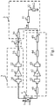
Fig.1 is a schematic diagram of the principle of a radio-frequency power amplifier circuit according to an embodiment of the application; -
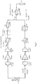
Fig.2 is a schematic diagram of an example of the radio-frequency power amplifier circuit according to an embodiment of the application; -
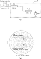
Fig.3 is a schematic diagram of an implementation of a combiner according to an embodiment of the application; -
Fig.4 is a schematic diagram of a load pulling effect in the traditional Doherty power amplifier circuit at 1.2GHz to 1.8GHz in the prior art; and -
Fig.5 is a schematic diagram of a load pulling effect in the Doherty power amplifier circuit at 1.2GHz to 1.8GHz according to an embodiment of the application. - In order to make the objects, technical solutions, and advantages of the embodiments of the application more apparent, the technical solutions according to the embodiments of the application will be described below clearly and fully with reference to the drawings in the embodiments of the application, and apparently the embodiments to be described below are only a part but not all of the embodiments of the application. Based upon the embodiments here of the application, all the other embodiments which can occur to those ordinarily skilled in the art without any inventive effort shall fall into the scope of the application.
- In order to address the narrowband characteristic of the traditional radio-frequency Doherty power amplifier circuit, the Doherty circuit structure is redesigned in the application to improve effectively the broadband performance of the Doherty power amplifier circuit so that the power amplifier can operate efficiently in multiple frequency bands.
- Preferable embodiments of the application will be described below in details with reference to the drawings.
- Referring to
Fig.1 , a redesigned Doherty power amplifier circuit according to an embodiment of the application includes apower distributor 1, acarrier amplifier branch 2, apeak amplifier branch 4, and acombiner 3 in that order, which are particularly connected in such a way that two ends of thepower distributor 1 are connected respectively with one end of thecarrier amplifier branch 2 and one end of thepeak amplifier branch 4, and the other end of thecarrier amplifier branch 2 and the other end of thepeak amplifier branch 4 are connected respectively with thecombiner 3. A series resonator circuit 5 is arranged between thecarrier amplifier branch 2 and thecombiner 3. The series resonator circuit 5 is configured to: appear inductive when an operating frequency of the Doherty power amplifier circuit above is higher than a central frequency, appear capacitive when the operating frequency of the Doherty power amplifier circuit above is lower than the central frequency, and have an impedance of 0 when the operating frequency of the Doherty power amplifier circuit above is the central frequency. - As illustrated in
Fig.1 , optionally thecarrier amplifier branch 2 includes a firstinput matching circuit 20, acarrier amplifier transistor 21, a firstoutput matching circuit 22, and a first offset line 23, all of which are connected in series. One end of the firstinput matching circuit 20 is connected with thepower distributor 1, and one end of the first offset line 23 is connected with the series resonator circuit 5. Preferably the carrier amplifier transistor 11 is a Laterally Diffused Metal Oxide Semiconductor, LDMOS, component or a gallium nitride (GaN) component, and a characteristic impedance of the first offset line 23 is 50 ohms. - As illustrated in
Fig.1 , thecombiner 3 includes a first λ/4impendence conversion line 30, a second λ/4impendence conversion line 31, and a first load 32, all of which are connected in series. Two ends of the first λ/4impendence conversion line 30 are connected respectively with the series resonator circuit 5 and thepeak amplifier branch 4. - As illustrated in
Fig.1 , thepeak amplifier branch 4 includes asecond offset line 40, a secondinput matching circuit 41, apeak amplifier transistor 42, a secondoutput matching circuit 43, a third λ/4impendence conversion line 44, and athird offset line 45, all of which are connected in series. One end of thesecond offset line 40 is connected with thepower distributor 1, and one end of thethird offset line 45 is connected with thecombiner 3. - As illustrated in
Fig.2 , in an embodiment, preferably the carrier amplifier transistor 11 is an LDMOS component or a GaN component, and a characteristic impendence of the first offset line 23 is 50 ohms Preferably a characteristic impendence of the first λ/4impendence conversion line 30 is 50 ohms, a characteristic impendence of the second λ/4impendence conversion line 31 is
peak amplifier transistor 42 is an LDMOS component or a GaN component, a characteristic impendence of the third λ/4impendence conversion line 44 is
third offset line 45 is
- As illustrated in
Fig.1 andFig.2 , thesecond offset line 40 is arranged to align thecarrier amplifier branch 2 in phase with thepeak amplifier branch 4, and preferably a characteristic impendence of thesecond offset line 40 is 50 ohms. - As illustrated in
Fig.1 andFig.2 , in an embodiment of the application combined with the design scheme of the traditional Doherty power amplifier circuit, the ratio of the maximum output capacity of thepeak amplifier transistor 42 to the maximum output capacity of thecarrier amplifier transistor 21 is an expected value a, that is, the maximum output capacity of the peak amplifier transistor divided by the maximum output capacity of the carrier amplifier transistor is a. In the traditional Doherty power amplifier circuit, the firstinput matching circuit 20 and the firstoutput matching circuit 22 can match the impendence of thecarrier amplifier transistor 21 with 50 ohms, and the secondinput matching circuit 41 and the secondoutput matching circuit 43 can match the impendence of thepeak amplifier transistor 42 with 50 ohms, in order for corresponding performance. The first offset line 23 with the characteristic impendence of 50 ohms in thecarrier amplifier branch 2, and the first λ/4impendence conversion line 30 with the characteristic impendence of 50 ohms in thecombiner 3 operate to modulate the load of thecarrier amplifier transistor 21 from 50 ohms to 50*a ohms given back-off power of -20log(1+a) dB in order for high efficiency. The third λ/4impendence conversion line 44 with the characteristic impendence of
peak amplifier branch 4 operates to convert the 50-ohm load impendence of thepeak amplifier transistor 42 to
peak amplifier transistor 42 to thecarrier amplifier transistor 21. Thethird offset line 45 with the characteristic impendence of
impendence conversion line 30, the third λ/4impendence conversion line 44, the first offset line 23, and thethird offset line 45. - In an embodiment of the application, the series resonator circuit 5 is added to the
carrier amplifier branch 2 to improve a bandwidth of the amplifier circuit, because the series resonator circuit 5 is characterized in that: it has an impendence of 0 when the operating frequency of the Doherty power amplifier circuit is the central frequency, appears inductive when the operating frequency of the Doherty power amplifier circuit is higher than the central frequency, and appears capacitive when the operating frequency of the Doherty power amplifier circuit is lower than the central frequency. The central frequency is the center of the entire bandwidth, and for example, the highest operating frequency is F1, and the lowest operating frequency is F2, given a bandwidth, so there is a central frequency of (F1+F2)/2. - Since the combiner in the traditional Doherty power amplifier circuit is characterized in that it appears capacitive when the operating frequency is higher than the central frequency, and appears inductive when the operating frequency is lower than the central frequency, apparently its characteristic is exactly opposite to that of the series resonator circuit 5, so the series resonator circuit 5 can counteract a reactance part of the Doherty power amplifier circuit in operation so that the input impendence of the combiner appears substantially only having the real part in a certain bandwidth to thereby extend effectively a load pulling bandwidth of the traditional Doherty power amplifier circuit.
- As illustrated in
Fig.3 , a load pulling effect in the traditional Doherty power amplifier circuit is achieved by the first λ/4impendence conversion line 30 of 50 ohms in thecombiner 3 given back-off power of -20log(1+a) dB; but the desirable load pulling effect can only be achieved at the central frequency, and the load pulling effect becomes poorer at a frequency further from the central frequency, due to the narrowband characteristic thereof. - As illustrated in
Fig.4 , taking the traditional Doherty power amplifier circuit including thecarrier amplifier transistor 21 and thepeak amplifier transistor 42, both of which are matched to 50 ohms as an example (suppose a symmetric structure, i.e., a=1, is adopted, and a load pulling effect in the frequency range of 1.2GHz to 1.8GHz is simulated),Fig.4 shows clearly the narrowband characteristic of the traditional Doherty power amplifier circuit. Particularly in the traditional Doherty power amplifier circuit, the first λ/4impendence conversion line 30 of 50 ohms with a narrowband characteristic cannot achieve load pulling effectively in the bandwidth; and as can be apparent fromFig.4 , the frequencies other than the central frequency are distributed on two sides of the real axis of the Smith chart (represented as the curve mlm2), and appear capacitive and inductive respectively, while an ideal load pulling effect is achieved until the real axis throughout the bandwidth, that is, the impedance of the combiner appears only having the real part, but not having the imaginary part. - As illustrated in
Fig.5 , taking the traditional Doherty power amplifier circuit including thecarrier amplifier transistor 21 and thepeak amplifier transistor 42, both of which are matched to 50 ohms as an example (suppose in a symmetric structure, i.e., a=1, is adopted, and a load pulling effect in the frequency range of 1.2GHz to 1.8GHz is simulated), particularly after the series resonator circuit 5 is added, a load pulling effect in the frequency range of 1.2GHz to 1.8GHz is changed from the curve X to the curve Y, and apparently the load pulling effect is in wider bandwidth, which approximates an ideal load pulling effect, after the series resonator circuit 5 is added, because the series resonator circuit 5 appears inductive when the operating frequency thereof is higher than the central frequency, appears capacitive when the operating frequency thereof is lower than the central frequency, and has an impendence of 0 when the operating frequency thereof is the central frequency. The series resonator circuit 5 is connected in series with the first λ/4impendence conversion line 30 of 50 ohms to thereby counteract a reactance part introduced by the first λ/4 impendence conversion line so as to improve effectively the bandwidth of the Doherty power amplifier circuit. - The newly designed Doherty power amplifier circuit above can also be applicable to a GaN component, and can be applicable to another circuit component adapted thereto, although a repeated description thereof will be omitted here.
- In summary, in embodiments of the application, the series resonator circuit is added to the traditional Doherty power amplifier circuit to thereby counteract a reactance introduced by the combiner in the traditional Doherty power amplifier circuit in operation, so as to improve the load pulling effect of the Doherty power amplifier circuit while operating efficiently, so that the load pulling effect is in wider bandwidth to enable a communication device to operate in multiple frequency bands and in multiple operating modes so as to lower the production and operating costs.
- Those skilled in the art shall appreciate that the embodiments of the application can be embodied as a method, a system or a computer program product. Therefore the application can be embodied in the form of an all-hardware embodiment, an all-software embodiment or an embodiment of software and hardware in combination. Furthermore the application can be embodied in the form of a computer program product embodied in one or more computer useable storage mediums (including but not limited to a disk memory, a CD-ROM, an optical memory, etc.) in which computer useable program codes are contained.
- The application has been described in a flow chart and/or a block diagram of the method, the device (system) and the computer program product according to the embodiments of the application. It shall be appreciated that respective flows and/or blocks in the flow chart and/or the block diagram and combinations of the flows and/or the blocks in the flow chart and/or the block diagram can be embodied in computer program instructions. These computer program instructions can be loaded onto a general-purpose computer, a specific-purpose computer, an embedded processor or a processor of another programmable data processing device to produce a machine so that the instructions executed on the computer or the processor of the other programmable data processing device create means for performing the functions specified in the flow(s) of the flow chart and/or the block(s) of the block diagram.
- These computer program instructions can also be stored into a computer readable memory capable of directing the computer or the other programmable data processing device to operate in a specific manner so that the instructions stored in the computer readable memory create an article of manufacture including instruction means which perform the functions specified in the flow(s) of the flow chart and/or the block(s) of the block diagram.
- These computer program instructions can also be loaded onto the computer or the other programmable data processing device so that a series of operational steps are performed on the computer or the other programmable data processing device to create a computer implemented process so that the instructions executed on the computer or the other programmable device provide steps for performing the functions specified in the flow(s) of the flow chart and/or the block(s) of the block diagram.
- Although the preferred embodiments of the application have been described, those skilled in the art benefiting from the underlying inventive concept can make additional modifications and variations to these embodiments. Therefore the appended claims are intended to be construed as encompassing the preferred embodiments and all the modifications and variations coming into the scope of the application.
- Evidently those skilled in the art can make various modifications and variations to the application without departing from the spirit and scope of the application. Thus the application is also intended to encompass these modifications and variations thereto so long as the modifications and variations come into the scope of the claims appended to the application and their equivalents.
Claims (7)
- A Doherty power amplifier circuit, comprising a power distributor (1), a carrier amplifier branch (2), a peak amplifier branch (4), and a combiner (3), wherein:
a series resonator circuit (5) is arranged between the carrier amplifier branch (2) and the combiner (3), and configured to: appear inductive when an operating frequency of the Doherty power amplifier circuit is higher than a central frequency, appear capacitive when the operating frequency of the Doherty power amplifier circuit is lower than the central frequency, and have an impedance of 0 when the operating frequency of the Doherty power amplifier circuit is the central frequency. - The Doherty power amplifier circuit according to claim 1, wherein the carrier amplifier branch (2) comprises a first input matching circuit (20), a carrier amplifier transistor (21), a first output matching circuit (22), and a first offset line (23), all of which are connected in series, wherein one end of the first input matching circuit (20) is connected with the power distributor (1), and one end of the first offset line (23) is connected with the series resonator circuit (5).
- The Doherty power amplifier circuit according to claim 2, wherein the carrier amplifier transistor (11) is a Laterally Diffused Metal Oxide Semiconductor, LDMOS, component or a gallium nitride (GaN) component, and a characteristic impedance of the first offset line (23) is 50 ohms.
- The Doherty power amplifier circuit according to claim 1, wherein the combiner (3) comprises a first λ/4 impendence conversion line (30), a second λ/4 impendence conversion line (31), and a first load (32), all of which are connected in series, wherein two ends of the first λ/4 impendence conversion line (30) are connected respectively with the series resonator circuit (5) and the peak amplifier branch (4), and λ represents a wavelength of an impendence conversion line.
- The Doherty power amplifier circuit according to claim 4, wherein a characteristic impendence of the first λ/4 impendence conversion line (30) is 50 ohms, a characteristic impendence of the second λ/4 impendence conversion line (31) is

- The Doherty power amplifier circuit according to claim 1, wherein the peak amplifier branch (4) comprises a second offset line (40), a second input matching circuit (41), a peak amplifier transistor (42), a second output matching circuit (43), a third λ/4 impendence conversion line (44), and a third offset line (45), all of which are connected in series, wherein one end of the second offset line (40) is connected with the power distributor (1), and one end of the third offset line (45) is connected with the combiner (3); and λ represents a wavelength of an impendence conversion line.
- The Doherty power amplifier circuit according to claim 6, wherein the peak amplifier transistor (42) is an LDMOS component or a GaN component, a characteristic impendence of the third λ/4 impendence conversion line (44) is


Applications Claiming Priority (2)
| Application Number | Priority Date | Filing Date | Title |
|---|---|---|---|
| CN201510645404.0A CN106571781B (en) | 2015-10-08 | 2015-10-08 | Doherty power amplifying circuit |
| PCT/CN2016/099605 WO2017059769A1 (en) | 2015-10-08 | 2016-09-21 | Doherty power amplifier circuit |
Publications (3)
| Publication Number | Publication Date |
|---|---|
| EP3361633A1 true EP3361633A1 (en) | 2018-08-15 |
| EP3361633A4 EP3361633A4 (en) | 2018-10-10 |
| EP3361633B1 EP3361633B1 (en) | 2021-05-05 |
Family
ID=58487235
Family Applications (1)
| Application Number | Title | Priority Date | Filing Date |
|---|---|---|---|
| EP16853074.9A Active EP3361633B1 (en) | 2015-10-08 | 2016-09-21 | Doherty power amplifier circuit |
Country Status (5)
| Country | Link |
|---|---|
| US (1) | US10511265B2 (en) |
| EP (1) | EP3361633B1 (en) |
| JP (1) | JP6616499B2 (en) |
| CN (1) | CN106571781B (en) |
| WO (1) | WO2017059769A1 (en) |
Families Citing this family (14)
| Publication number | Priority date | Publication date | Assignee | Title |
|---|---|---|---|---|
| CN107547051B (en) * | 2017-08-28 | 2020-10-23 | 广东顺德中山大学卡内基梅隆大学国际联合研究院 | Doherty power amplifier based on distributed broadband impedance transformation structure |
| EP3729640A4 (en) | 2017-12-19 | 2021-07-14 | Telefonaktiebolaget LM Ericsson (publ) | Power amplifier and radio frequency device comprising the same |
| CN109672411B (en) * | 2018-12-19 | 2023-02-28 | 重庆邮电大学 | Asymmetric broadband Doherty power amplifier suitable for 5G low-frequency band full frequency band |
| DE112019007775T5 (en) * | 2019-10-02 | 2022-06-15 | Mitsubishi Electric Corporation | Doherty amplifier |
| US10868500B1 (en) | 2019-10-29 | 2020-12-15 | Nxp Usa, Inc. | Doherty amplifier with complex combining load matching circuit |
| US10862434B1 (en) * | 2019-10-29 | 2020-12-08 | Nxp Usa, Inc. | Asymmetric Doherty amplifier with complex combining load matching circuit |
| CN113014205B (en) * | 2019-12-19 | 2024-09-24 | 苏州华太电子技术股份有限公司 | Asymmetric Doherty power amplifier, matching circuit thereof and implementation method of matching circuit |
| US11522497B2 (en) | 2020-05-26 | 2022-12-06 | Nxp Usa, Inc. | Doherty amplifier incorporating output matching network with integrated passive devices |
| US11750156B2 (en) | 2020-08-24 | 2023-09-05 | City University Of Hong Kong | Power amplifier |
| US11616476B2 (en) | 2020-10-19 | 2023-03-28 | City University Of Hong Kong | Power amplifier circuit |
| US12034408B2 (en) | 2020-11-16 | 2024-07-09 | City University Of Hong Kong | Wideband Doherty power amplifier |
| CN114553149A (en) * | 2020-11-24 | 2022-05-27 | 苏州华太电子技术有限公司 | Doherty radio frequency power amplifier module based on novel DraaMOS (DraaMOS) process and output matching network thereof |
| CN112491365B (en) * | 2020-12-29 | 2021-09-10 | 南京米乐为微电子科技有限公司 | Broadband Doherty power amplifier based on single parallel resonance block |
| CN119696519A (en) * | 2024-11-29 | 2025-03-25 | 重庆邮电大学 | A GaN-based mode-reconfigurable Doherty power amplifier |
Family Cites Families (21)
| Publication number | Priority date | Publication date | Assignee | Title |
|---|---|---|---|---|
| JP2002118428A (en) * | 2000-10-06 | 2002-04-19 | Matsushita Electric Ind Co Ltd | High frequency amplifier |
| KR100546491B1 (en) * | 2001-03-21 | 2006-01-26 | 학교법인 포항공과대학교 | Output Matching Device for Microwave Doherty Amplifiers |
| JP4700470B2 (en) * | 2004-12-15 | 2011-06-15 | 株式会社日立国際電気 | amplifier |
| CN100426662C (en) * | 2006-03-22 | 2008-10-15 | 华为技术有限公司 | Power amplifier |
| JP5217182B2 (en) * | 2007-02-22 | 2013-06-19 | 富士通株式会社 | High frequency amplifier circuit |
| KR101102128B1 (en) * | 2009-12-15 | 2012-01-02 | 서울대학교산학협력단 | E power amplifier |
| KR101677555B1 (en) * | 2010-02-25 | 2016-11-21 | 삼성전자주식회사 | Apparatus for improving performance at low power region in doherty amplifier |
| CN102142812B (en) | 2010-12-17 | 2013-08-28 | 华为技术有限公司 | Doherty power amplifier |
| US8717102B2 (en) * | 2011-09-27 | 2014-05-06 | Infineon Technologies Ag | RF device with compensatory resonator matching topology |
| US8502599B2 (en) * | 2011-10-19 | 2013-08-06 | Futurewei Technologies, Inc. | System and method for a multi-band power-amplifier |
| JP5874441B2 (en) * | 2012-02-29 | 2016-03-02 | 富士通株式会社 | amplifier |
| EP2870691A1 (en) * | 2012-07-05 | 2015-05-13 | Telefonaktiebolaget LM Ericsson (Publ) | Amplifier device and corresponding radio base station and mobile communication terminal |
| CN103107778B (en) | 2012-12-31 | 2016-03-02 | 东南大学 | A kind of Doherty power amplifier and adjustment method thereof reducing third order intermodulation |
| CN104218897A (en) | 2013-05-31 | 2014-12-17 | 诺基亚公司 | Device and method for providing efficient and compact Doherty power amplifier |
| US9397616B2 (en) * | 2013-11-06 | 2016-07-19 | Commscope Technologies Llc | Quasi-doherty architecture amplifier and method |
| CN203800892U (en) | 2014-02-28 | 2014-08-27 | 上海无线电设备研究所 | High-linearity power amplifier |
| JP6558360B2 (en) * | 2014-03-06 | 2019-08-14 | 日本電気株式会社 | Transmitter, transmission method |
| CN104113286B (en) * | 2014-07-10 | 2017-08-04 | 大唐移动通信设备有限公司 | Doherty power amplifying circuit |
| WO2016203512A1 (en) * | 2015-06-15 | 2016-12-22 | 株式会社日立国際電気 | Power amplifier and radio transmitter |
| DE112016006472T5 (en) * | 2016-02-23 | 2018-11-08 | Mitsubishi Electric Corporation | LAST MODULATION AMPLIFIER |
| US10284147B2 (en) * | 2016-12-15 | 2019-05-07 | Nxp Usa, Inc. | Doherty amplifiers and amplifier modules with shunt inductance circuits that affect transmission line length between carrier and peaking amplifier outputs |
-
2015
- 2015-10-08 CN CN201510645404.0A patent/CN106571781B/en active Active
-
2016
- 2016-09-21 US US15/767,135 patent/US10511265B2/en active Active
- 2016-09-21 JP JP2018517726A patent/JP6616499B2/en active Active
- 2016-09-21 EP EP16853074.9A patent/EP3361633B1/en active Active
- 2016-09-21 WO PCT/CN2016/099605 patent/WO2017059769A1/en not_active Ceased
Also Published As
| Publication number | Publication date |
|---|---|
| JP6616499B2 (en) | 2019-12-04 |
| CN106571781A (en) | 2017-04-19 |
| EP3361633A4 (en) | 2018-10-10 |
| JP2018530263A (en) | 2018-10-11 |
| WO2017059769A1 (en) | 2017-04-13 |
| EP3361633B1 (en) | 2021-05-05 |
| US20190074799A1 (en) | 2019-03-07 |
| CN106571781B (en) | 2020-09-25 |
| US10511265B2 (en) | 2019-12-17 |
Similar Documents
| Publication | Publication Date | Title |
|---|---|---|
| US10511265B2 (en) | Doherty power amplifier circuit | |
| EP3010144B1 (en) | Switchable dual core power amplifier | |
| EP2713505B1 (en) | Doherty power amplifier and signal processing method | |
| US20220166384A1 (en) | No-load-modulation, high-efficiency power amplifier | |
| US9215120B2 (en) | Multi-band crest factor reduction | |
| EP2887541A1 (en) | Enhanced and versatile N-way doherty power amplifier | |
| CN107210710B (en) | Three-way sequential power amplifier | |
| EP2541759A1 (en) | Doherty power amplifier and implementation method therefor | |
| CN110266275A (en) | A Hybrid Broadband Doherty Power Amplifier of Continuous Inverse Class F and Class J | |
| US20140035679A1 (en) | Power Amplifier Device and Power Amplifier Circuit Thereof | |
| CN104113286B (en) | Doherty power amplifying circuit | |
| US12368458B2 (en) | Multistage doherty power amplifier and transmitter | |
| US11411540B2 (en) | Power amplifier and radio frequency device comprising the same | |
| CN106374863A (en) | Doherty power amplifier capable of improving power back-off dynamic range and realization method thereof | |
| Han et al. | Dual-mode dual-band symmetrical Doherty power amplifier employing reciprocal gate bias for high-efficiency range enhancement | |
| US8797099B2 (en) | Power amplifier device and power amplifier circuit thereof | |
| US10224878B2 (en) | Power amplification device | |
| Manni et al. | A waveform engineering approach for class F operation in a class C biased peaking branch of GaN MMIC Doherty power amplifiers | |
| US20210250208A1 (en) | Method and apparatus for envelope shaping of multi-carrier signal in envelope tracking transmission | |
| Ghannouchi et al. | Doherty power amplifiers in software radio systems | |
| Wang et al. | Envelope Tracking Line-up Design Considerations with High Efficiency Linearizable Inverse Class-F Driver Amplifier |
Legal Events
| Date | Code | Title | Description |
|---|---|---|---|
| STAA | Information on the status of an ep patent application or granted ep patent |
Free format text: STATUS: THE INTERNATIONAL PUBLICATION HAS BEEN MADE |
|
| PUAI | Public reference made under article 153(3) epc to a published international application that has entered the european phase |
Free format text: ORIGINAL CODE: 0009012 |
|
| STAA | Information on the status of an ep patent application or granted ep patent |
Free format text: STATUS: REQUEST FOR EXAMINATION WAS MADE |
|
| 17P | Request for examination filed |
Effective date: 20180413 |
|
| AK | Designated contracting states |
Kind code of ref document: A1 Designated state(s): AL AT BE BG CH CY CZ DE DK EE ES FI FR GB GR HR HU IE IS IT LI LT LU LV MC MK MT NL NO PL PT RO RS SE SI SK SM TR |
|
| AX | Request for extension of the european patent |
Extension state: BA ME |
|
| REG | Reference to a national code |
Ref country code: DE Ref legal event code: R079 Ref document number: 602016057553 Country of ref document: DE Free format text: PREVIOUS MAIN CLASS: H03F0001420000 Ipc: H03F0001020000 |
|
| A4 | Supplementary search report drawn up and despatched |
Effective date: 20180907 |
|
| RIC1 | Information provided on ipc code assigned before grant |
Ipc: H03F 1/56 20060101ALI20180901BHEP Ipc: H03F 1/02 20060101AFI20180901BHEP Ipc: H03F 1/42 20060101ALI20180901BHEP |
|
| DAV | Request for validation of the european patent (deleted) | ||
| DAX | Request for extension of the european patent (deleted) | ||
| GRAP | Despatch of communication of intention to grant a patent |
Free format text: ORIGINAL CODE: EPIDOSNIGR1 |
|
| STAA | Information on the status of an ep patent application or granted ep patent |
Free format text: STATUS: GRANT OF PATENT IS INTENDED |
|
| INTG | Intention to grant announced |
Effective date: 20210120 |
|
| GRAS | Grant fee paid |
Free format text: ORIGINAL CODE: EPIDOSNIGR3 |
|
| GRAA | (expected) grant |
Free format text: ORIGINAL CODE: 0009210 |
|
| STAA | Information on the status of an ep patent application or granted ep patent |
Free format text: STATUS: THE PATENT HAS BEEN GRANTED |
|
| AK | Designated contracting states |
Kind code of ref document: B1 Designated state(s): AL AT BE BG CH CY CZ DE DK EE ES FI FR GB GR HR HU IE IS IT LI LT LU LV MC MK MT NL NO PL PT RO RS SE SI SK SM TR |
|
| REG | Reference to a national code |
Ref country code: GB Ref legal event code: FG4D |
|
| REG | Reference to a national code |
Ref country code: CH Ref legal event code: EP |
|
| REG | Reference to a national code |
Ref country code: AT Ref legal event code: REF Ref document number: 1391099 Country of ref document: AT Kind code of ref document: T Effective date: 20210515 |
|
| REG | Reference to a national code |
Ref country code: IE Ref legal event code: FG4D |
|
| REG | Reference to a national code |
Ref country code: DE Ref legal event code: R096 Ref document number: 602016057553 Country of ref document: DE |
|
| REG | Reference to a national code |
Ref country code: LT Ref legal event code: MG9D |
|
| REG | Reference to a national code |
Ref country code: AT Ref legal event code: MK05 Ref document number: 1391099 Country of ref document: AT Kind code of ref document: T Effective date: 20210505 |
|
| PG25 | Lapsed in a contracting state [announced via postgrant information from national office to epo] |
Ref country code: BG Free format text: LAPSE BECAUSE OF FAILURE TO SUBMIT A TRANSLATION OF THE DESCRIPTION OR TO PAY THE FEE WITHIN THE PRESCRIBED TIME-LIMIT Effective date: 20210805 Ref country code: AT Free format text: LAPSE BECAUSE OF FAILURE TO SUBMIT A TRANSLATION OF THE DESCRIPTION OR TO PAY THE FEE WITHIN THE PRESCRIBED TIME-LIMIT Effective date: 20210505 Ref country code: HR Free format text: LAPSE BECAUSE OF FAILURE TO SUBMIT A TRANSLATION OF THE DESCRIPTION OR TO PAY THE FEE WITHIN THE PRESCRIBED TIME-LIMIT Effective date: 20210505 Ref country code: FI Free format text: LAPSE BECAUSE OF FAILURE TO SUBMIT A TRANSLATION OF THE DESCRIPTION OR TO PAY THE FEE WITHIN THE PRESCRIBED TIME-LIMIT Effective date: 20210505 Ref country code: LT Free format text: LAPSE BECAUSE OF FAILURE TO SUBMIT A TRANSLATION OF THE DESCRIPTION OR TO PAY THE FEE WITHIN THE PRESCRIBED TIME-LIMIT Effective date: 20210505 |
|
| PG25 | Lapsed in a contracting state [announced via postgrant information from national office to epo] |
Ref country code: PL Free format text: LAPSE BECAUSE OF FAILURE TO SUBMIT A TRANSLATION OF THE DESCRIPTION OR TO PAY THE FEE WITHIN THE PRESCRIBED TIME-LIMIT Effective date: 20210505 Ref country code: NO Free format text: LAPSE BECAUSE OF FAILURE TO SUBMIT A TRANSLATION OF THE DESCRIPTION OR TO PAY THE FEE WITHIN THE PRESCRIBED TIME-LIMIT Effective date: 20210805 Ref country code: PT Free format text: LAPSE BECAUSE OF FAILURE TO SUBMIT A TRANSLATION OF THE DESCRIPTION OR TO PAY THE FEE WITHIN THE PRESCRIBED TIME-LIMIT Effective date: 20210906 Ref country code: RS Free format text: LAPSE BECAUSE OF FAILURE TO SUBMIT A TRANSLATION OF THE DESCRIPTION OR TO PAY THE FEE WITHIN THE PRESCRIBED TIME-LIMIT Effective date: 20210505 Ref country code: SE Free format text: LAPSE BECAUSE OF FAILURE TO SUBMIT A TRANSLATION OF THE DESCRIPTION OR TO PAY THE FEE WITHIN THE PRESCRIBED TIME-LIMIT Effective date: 20210505 Ref country code: IS Free format text: LAPSE BECAUSE OF FAILURE TO SUBMIT A TRANSLATION OF THE DESCRIPTION OR TO PAY THE FEE WITHIN THE PRESCRIBED TIME-LIMIT Effective date: 20210905 Ref country code: GR Free format text: LAPSE BECAUSE OF FAILURE TO SUBMIT A TRANSLATION OF THE DESCRIPTION OR TO PAY THE FEE WITHIN THE PRESCRIBED TIME-LIMIT Effective date: 20210806 Ref country code: LV Free format text: LAPSE BECAUSE OF FAILURE TO SUBMIT A TRANSLATION OF THE DESCRIPTION OR TO PAY THE FEE WITHIN THE PRESCRIBED TIME-LIMIT Effective date: 20210505 |
|
| REG | Reference to a national code |
Ref country code: NL Ref legal event code: MP Effective date: 20210505 |
|
| PG25 | Lapsed in a contracting state [announced via postgrant information from national office to epo] |
Ref country code: NL Free format text: LAPSE BECAUSE OF FAILURE TO SUBMIT A TRANSLATION OF THE DESCRIPTION OR TO PAY THE FEE WITHIN THE PRESCRIBED TIME-LIMIT Effective date: 20210505 |
|
| PG25 | Lapsed in a contracting state [announced via postgrant information from national office to epo] |
Ref country code: DK Free format text: LAPSE BECAUSE OF FAILURE TO SUBMIT A TRANSLATION OF THE DESCRIPTION OR TO PAY THE FEE WITHIN THE PRESCRIBED TIME-LIMIT Effective date: 20210505 Ref country code: EE Free format text: LAPSE BECAUSE OF FAILURE TO SUBMIT A TRANSLATION OF THE DESCRIPTION OR TO PAY THE FEE WITHIN THE PRESCRIBED TIME-LIMIT Effective date: 20210505 Ref country code: CZ Free format text: LAPSE BECAUSE OF FAILURE TO SUBMIT A TRANSLATION OF THE DESCRIPTION OR TO PAY THE FEE WITHIN THE PRESCRIBED TIME-LIMIT Effective date: 20210505 Ref country code: ES Free format text: LAPSE BECAUSE OF FAILURE TO SUBMIT A TRANSLATION OF THE DESCRIPTION OR TO PAY THE FEE WITHIN THE PRESCRIBED TIME-LIMIT Effective date: 20210505 Ref country code: RO Free format text: LAPSE BECAUSE OF FAILURE TO SUBMIT A TRANSLATION OF THE DESCRIPTION OR TO PAY THE FEE WITHIN THE PRESCRIBED TIME-LIMIT Effective date: 20210505 Ref country code: SK Free format text: LAPSE BECAUSE OF FAILURE TO SUBMIT A TRANSLATION OF THE DESCRIPTION OR TO PAY THE FEE WITHIN THE PRESCRIBED TIME-LIMIT Effective date: 20210505 Ref country code: SM Free format text: LAPSE BECAUSE OF FAILURE TO SUBMIT A TRANSLATION OF THE DESCRIPTION OR TO PAY THE FEE WITHIN THE PRESCRIBED TIME-LIMIT Effective date: 20210505 |
|
| REG | Reference to a national code |
Ref country code: DE Ref legal event code: R097 Ref document number: 602016057553 Country of ref document: DE |
|
| PLBE | No opposition filed within time limit |
Free format text: ORIGINAL CODE: 0009261 |
|
| STAA | Information on the status of an ep patent application or granted ep patent |
Free format text: STATUS: NO OPPOSITION FILED WITHIN TIME LIMIT |
|
| 26N | No opposition filed |
Effective date: 20220208 |
|
| REG | Reference to a national code |
Ref country code: CH Ref legal event code: PL |
|
| REG | Reference to a national code |
Ref country code: BE Ref legal event code: MM Effective date: 20210930 |
|
| PG25 | Lapsed in a contracting state [announced via postgrant information from national office to epo] |
Ref country code: IS Free format text: LAPSE BECAUSE OF FAILURE TO SUBMIT A TRANSLATION OF THE DESCRIPTION OR TO PAY THE FEE WITHIN THE PRESCRIBED TIME-LIMIT Effective date: 20210905 Ref country code: MC Free format text: LAPSE BECAUSE OF FAILURE TO SUBMIT A TRANSLATION OF THE DESCRIPTION OR TO PAY THE FEE WITHIN THE PRESCRIBED TIME-LIMIT Effective date: 20210505 Ref country code: AL Free format text: LAPSE BECAUSE OF FAILURE TO SUBMIT A TRANSLATION OF THE DESCRIPTION OR TO PAY THE FEE WITHIN THE PRESCRIBED TIME-LIMIT Effective date: 20210505 |
|
| PG25 | Lapsed in a contracting state [announced via postgrant information from national office to epo] |
Ref country code: BE Free format text: LAPSE BECAUSE OF NON-PAYMENT OF DUE FEES Effective date: 20210930 Ref country code: LU Free format text: LAPSE BECAUSE OF NON-PAYMENT OF DUE FEES Effective date: 20210921 Ref country code: IT Free format text: LAPSE BECAUSE OF FAILURE TO SUBMIT A TRANSLATION OF THE DESCRIPTION OR TO PAY THE FEE WITHIN THE PRESCRIBED TIME-LIMIT Effective date: 20210505 Ref country code: IE Free format text: LAPSE BECAUSE OF NON-PAYMENT OF DUE FEES Effective date: 20210921 |
|
| PG25 | Lapsed in a contracting state [announced via postgrant information from national office to epo] |
Ref country code: LI Free format text: LAPSE BECAUSE OF NON-PAYMENT OF DUE FEES Effective date: 20210930 Ref country code: CH Free format text: LAPSE BECAUSE OF NON-PAYMENT OF DUE FEES Effective date: 20210930 |
|
| PG25 | Lapsed in a contracting state [announced via postgrant information from national office to epo] |
Ref country code: CY Free format text: LAPSE BECAUSE OF FAILURE TO SUBMIT A TRANSLATION OF THE DESCRIPTION OR TO PAY THE FEE WITHIN THE PRESCRIBED TIME-LIMIT Effective date: 20210505 |
|
| PG25 | Lapsed in a contracting state [announced via postgrant information from national office to epo] |
Ref country code: HU Free format text: LAPSE BECAUSE OF FAILURE TO SUBMIT A TRANSLATION OF THE DESCRIPTION OR TO PAY THE FEE WITHIN THE PRESCRIBED TIME-LIMIT; INVALID AB INITIO Effective date: 20160921 |
|
| PG25 | Lapsed in a contracting state [announced via postgrant information from national office to epo] |
Ref country code: MK Free format text: LAPSE BECAUSE OF FAILURE TO SUBMIT A TRANSLATION OF THE DESCRIPTION OR TO PAY THE FEE WITHIN THE PRESCRIBED TIME-LIMIT Effective date: 20210505 |
|
| PG25 | Lapsed in a contracting state [announced via postgrant information from national office to epo] |
Ref country code: TR Free format text: LAPSE BECAUSE OF FAILURE TO SUBMIT A TRANSLATION OF THE DESCRIPTION OR TO PAY THE FEE WITHIN THE PRESCRIBED TIME-LIMIT Effective date: 20210505 |
|
| PG25 | Lapsed in a contracting state [announced via postgrant information from national office to epo] |
Ref country code: MT Free format text: LAPSE BECAUSE OF FAILURE TO SUBMIT A TRANSLATION OF THE DESCRIPTION OR TO PAY THE FEE WITHIN THE PRESCRIBED TIME-LIMIT Effective date: 20210505 |
|
| PGFP | Annual fee paid to national office [announced via postgrant information from national office to epo] |
Ref country code: DE Payment date: 20250919 Year of fee payment: 10 |
|
| PGFP | Annual fee paid to national office [announced via postgrant information from national office to epo] |
Ref country code: GB Payment date: 20250919 Year of fee payment: 10 |
|
| PGFP | Annual fee paid to national office [announced via postgrant information from national office to epo] |
Ref country code: FR Payment date: 20250922 Year of fee payment: 10 |