EP3361510A1 - Graphene nanoribbon, graphene nanoribbon fabrication method, and semiconductor device - Google Patents
Graphene nanoribbon, graphene nanoribbon fabrication method, and semiconductor device Download PDFInfo
- Publication number
- EP3361510A1 EP3361510A1 EP18155338.9A EP18155338A EP3361510A1 EP 3361510 A1 EP3361510 A1 EP 3361510A1 EP 18155338 A EP18155338 A EP 18155338A EP 3361510 A1 EP3361510 A1 EP 3361510A1
- Authority
- EP
- European Patent Office
- Prior art keywords
- graphene nanoribbon
- edge
- bonded
- graphene
- group
- Prior art date
- Legal status (The legal status is an assumption and is not a legal conclusion. Google has not performed a legal analysis and makes no representation as to the accuracy of the status listed.)
- Granted
Links
Images


Classifications
-
- H—ELECTRICITY
- H10—SEMICONDUCTOR DEVICES; ELECTRIC SOLID-STATE DEVICES NOT OTHERWISE PROVIDED FOR
- H10D—INORGANIC ELECTRIC SEMICONDUCTOR DEVICES
- H10D62/00—Semiconductor bodies, or regions thereof, of devices having potential barriers
- H10D62/80—Semiconductor bodies, or regions thereof, of devices having potential barriers characterised by the materials
- H10D62/881—Semiconductor bodies, or regions thereof, of devices having potential barriers characterised by the materials being a two-dimensional material
- H10D62/882—Graphene
-
- B—PERFORMING OPERATIONS; TRANSPORTING
- B82—NANOTECHNOLOGY
- B82Y—SPECIFIC USES OR APPLICATIONS OF NANOSTRUCTURES; MEASUREMENT OR ANALYSIS OF NANOSTRUCTURES; MANUFACTURE OR TREATMENT OF NANOSTRUCTURES
- B82Y30/00—Nanotechnology for materials or surface science, e.g. nanocomposites
-
- B—PERFORMING OPERATIONS; TRANSPORTING
- B82—NANOTECHNOLOGY
- B82Y—SPECIFIC USES OR APPLICATIONS OF NANOSTRUCTURES; MEASUREMENT OR ANALYSIS OF NANOSTRUCTURES; MANUFACTURE OR TREATMENT OF NANOSTRUCTURES
- B82Y40/00—Manufacture or treatment of nanostructures
-
- C—CHEMISTRY; METALLURGY
- C01—INORGANIC CHEMISTRY
- C01B—NON-METALLIC ELEMENTS; COMPOUNDS THEREOF; METALLOIDS OR COMPOUNDS THEREOF NOT COVERED BY SUBCLASS C01C
- C01B32/00—Carbon; Compounds thereof
- C01B32/15—Nano-sized carbon materials
- C01B32/182—Graphene
- C01B32/184—Preparation
-
- C—CHEMISTRY; METALLURGY
- C08—ORGANIC MACROMOLECULAR COMPOUNDS; THEIR PREPARATION OR CHEMICAL WORKING-UP; COMPOSITIONS BASED THEREON
- C08G—MACROMOLECULAR COMPOUNDS OBTAINED OTHERWISE THAN BY REACTIONS ONLY INVOLVING UNSATURATED CARBON-TO-CARBON BONDS
- C08G61/00—Macromolecular compounds obtained by reactions forming a carbon-to-carbon link in the main chain of the macromolecule
- C08G61/12—Macromolecular compounds containing atoms other than carbon in the main chain of the macromolecule
-
- C—CHEMISTRY; METALLURGY
- C08—ORGANIC MACROMOLECULAR COMPOUNDS; THEIR PREPARATION OR CHEMICAL WORKING-UP; COMPOSITIONS BASED THEREON
- C08G—MACROMOLECULAR COMPOUNDS OBTAINED OTHERWISE THAN BY REACTIONS ONLY INVOLVING UNSATURATED CARBON-TO-CARBON BONDS
- C08G61/00—Macromolecular compounds obtained by reactions forming a carbon-to-carbon link in the main chain of the macromolecule
- C08G61/12—Macromolecular compounds containing atoms other than carbon in the main chain of the macromolecule
- C08G61/122—Macromolecular compounds containing atoms other than carbon in the main chain of the macromolecule derived from five- or six-membered heterocyclic compounds, other than imides
-
- H—ELECTRICITY
- H10—SEMICONDUCTOR DEVICES; ELECTRIC SOLID-STATE DEVICES NOT OTHERWISE PROVIDED FOR
- H10K—ORGANIC ELECTRIC SOLID-STATE DEVICES
- H10K10/00—Organic devices specially adapted for rectifying, amplifying, oscillating or switching; Organic capacitors or resistors having potential barriers
- H10K10/40—Organic transistors
- H10K10/46—Field-effect transistors, e.g. organic thin-film transistors [OTFT]
- H10K10/462—Insulated gate field-effect transistors [IGFETs]
- H10K10/464—Lateral top-gate IGFETs comprising only a single gate
-
- H—ELECTRICITY
- H10—SEMICONDUCTOR DEVICES; ELECTRIC SOLID-STATE DEVICES NOT OTHERWISE PROVIDED FOR
- H10K—ORGANIC ELECTRIC SOLID-STATE DEVICES
- H10K10/00—Organic devices specially adapted for rectifying, amplifying, oscillating or switching; Organic capacitors or resistors having potential barriers
- H10K10/40—Organic transistors
- H10K10/46—Field-effect transistors, e.g. organic thin-film transistors [OTFT]
- H10K10/462—Insulated gate field-effect transistors [IGFETs]
- H10K10/466—Lateral bottom-gate IGFETs comprising only a single gate
-
- H—ELECTRICITY
- H10—SEMICONDUCTOR DEVICES; ELECTRIC SOLID-STATE DEVICES NOT OTHERWISE PROVIDED FOR
- H10K—ORGANIC ELECTRIC SOLID-STATE DEVICES
- H10K85/00—Organic materials used in the body or electrodes of devices covered by this subclass
- H10K85/20—Carbon compounds, e.g. carbon nanotubes or fullerenes
-
- C—CHEMISTRY; METALLURGY
- C08—ORGANIC MACROMOLECULAR COMPOUNDS; THEIR PREPARATION OR CHEMICAL WORKING-UP; COMPOSITIONS BASED THEREON
- C08G—MACROMOLECULAR COMPOUNDS OBTAINED OTHERWISE THAN BY REACTIONS ONLY INVOLVING UNSATURATED CARBON-TO-CARBON BONDS
- C08G2261/00—Macromolecular compounds obtained by reactions forming a carbon-to-carbon link in the main chain of the macromolecule
- C08G2261/10—Definition of the polymer structure
- C08G2261/11—Homopolymers
-
- C—CHEMISTRY; METALLURGY
- C08—ORGANIC MACROMOLECULAR COMPOUNDS; THEIR PREPARATION OR CHEMICAL WORKING-UP; COMPOSITIONS BASED THEREON
- C08G—MACROMOLECULAR COMPOUNDS OBTAINED OTHERWISE THAN BY REACTIONS ONLY INVOLVING UNSATURATED CARBON-TO-CARBON BONDS
- C08G2261/00—Macromolecular compounds obtained by reactions forming a carbon-to-carbon link in the main chain of the macromolecule
- C08G2261/10—Definition of the polymer structure
- C08G2261/13—Morphological aspects
-
- C—CHEMISTRY; METALLURGY
- C08—ORGANIC MACROMOLECULAR COMPOUNDS; THEIR PREPARATION OR CHEMICAL WORKING-UP; COMPOSITIONS BASED THEREON
- C08G—MACROMOLECULAR COMPOUNDS OBTAINED OTHERWISE THAN BY REACTIONS ONLY INVOLVING UNSATURATED CARBON-TO-CARBON BONDS
- C08G2261/00—Macromolecular compounds obtained by reactions forming a carbon-to-carbon link in the main chain of the macromolecule
- C08G2261/10—Definition of the polymer structure
- C08G2261/22—Molecular weight
- C08G2261/228—Polymers, i.e. more than 10 repeat units
-
- C—CHEMISTRY; METALLURGY
- C08—ORGANIC MACROMOLECULAR COMPOUNDS; THEIR PREPARATION OR CHEMICAL WORKING-UP; COMPOSITIONS BASED THEREON
- C08G—MACROMOLECULAR COMPOUNDS OBTAINED OTHERWISE THAN BY REACTIONS ONLY INVOLVING UNSATURATED CARBON-TO-CARBON BONDS
- C08G2261/00—Macromolecular compounds obtained by reactions forming a carbon-to-carbon link in the main chain of the macromolecule
- C08G2261/30—Monomer units or repeat units incorporating structural elements in the main chain
- C08G2261/32—Monomer units or repeat units incorporating structural elements in the main chain incorporating heteroaromatic structural elements in the main chain
- C08G2261/324—Monomer units or repeat units incorporating structural elements in the main chain incorporating heteroaromatic structural elements in the main chain condensed
- C08G2261/3241—Monomer units or repeat units incorporating structural elements in the main chain incorporating heteroaromatic structural elements in the main chain condensed containing one or more nitrogen atoms as the only heteroatom, e.g. carbazole
-
- C—CHEMISTRY; METALLURGY
- C08—ORGANIC MACROMOLECULAR COMPOUNDS; THEIR PREPARATION OR CHEMICAL WORKING-UP; COMPOSITIONS BASED THEREON
- C08G—MACROMOLECULAR COMPOUNDS OBTAINED OTHERWISE THAN BY REACTIONS ONLY INVOLVING UNSATURATED CARBON-TO-CARBON BONDS
- C08G2261/00—Macromolecular compounds obtained by reactions forming a carbon-to-carbon link in the main chain of the macromolecule
- C08G2261/30—Monomer units or repeat units incorporating structural elements in the main chain
- C08G2261/32—Monomer units or repeat units incorporating structural elements in the main chain incorporating heteroaromatic structural elements in the main chain
- C08G2261/324—Monomer units or repeat units incorporating structural elements in the main chain incorporating heteroaromatic structural elements in the main chain condensed
- C08G2261/3242—Monomer units or repeat units incorporating structural elements in the main chain incorporating heteroaromatic structural elements in the main chain condensed containing one or more oxygen atoms as the only heteroatom, e.g. benzofuran
-
- C—CHEMISTRY; METALLURGY
- C08—ORGANIC MACROMOLECULAR COMPOUNDS; THEIR PREPARATION OR CHEMICAL WORKING-UP; COMPOSITIONS BASED THEREON
- C08G—MACROMOLECULAR COMPOUNDS OBTAINED OTHERWISE THAN BY REACTIONS ONLY INVOLVING UNSATURATED CARBON-TO-CARBON BONDS
- C08G2261/00—Macromolecular compounds obtained by reactions forming a carbon-to-carbon link in the main chain of the macromolecule
- C08G2261/70—Post-treatment
- C08G2261/72—Derivatisation
- C08G2261/724—Hydrogenation
-
- C—CHEMISTRY; METALLURGY
- C08—ORGANIC MACROMOLECULAR COMPOUNDS; THEIR PREPARATION OR CHEMICAL WORKING-UP; COMPOSITIONS BASED THEREON
- C08G—MACROMOLECULAR COMPOUNDS OBTAINED OTHERWISE THAN BY REACTIONS ONLY INVOLVING UNSATURATED CARBON-TO-CARBON BONDS
- C08G2261/00—Macromolecular compounds obtained by reactions forming a carbon-to-carbon link in the main chain of the macromolecule
- C08G2261/90—Applications
- C08G2261/91—Photovoltaic applications
-
- C—CHEMISTRY; METALLURGY
- C08—ORGANIC MACROMOLECULAR COMPOUNDS; THEIR PREPARATION OR CHEMICAL WORKING-UP; COMPOSITIONS BASED THEREON
- C08G—MACROMOLECULAR COMPOUNDS OBTAINED OTHERWISE THAN BY REACTIONS ONLY INVOLVING UNSATURATED CARBON-TO-CARBON BONDS
- C08G2261/00—Macromolecular compounds obtained by reactions forming a carbon-to-carbon link in the main chain of the macromolecule
- C08G2261/90—Applications
- C08G2261/92—TFT applications
-
- H—ELECTRICITY
- H10—SEMICONDUCTOR DEVICES; ELECTRIC SOLID-STATE DEVICES NOT OTHERWISE PROVIDED FOR
- H10K—ORGANIC ELECTRIC SOLID-STATE DEVICES
- H10K10/00—Organic devices specially adapted for rectifying, amplifying, oscillating or switching; Organic capacitors or resistors having potential barriers
- H10K10/20—Organic diodes
- H10K10/23—Schottky diodes
-
- H—ELECTRICITY
- H10—SEMICONDUCTOR DEVICES; ELECTRIC SOLID-STATE DEVICES NOT OTHERWISE PROVIDED FOR
- H10K—ORGANIC ELECTRIC SOLID-STATE DEVICES
- H10K10/00—Organic devices specially adapted for rectifying, amplifying, oscillating or switching; Organic capacitors or resistors having potential barriers
- H10K10/40—Organic transistors
- H10K10/46—Field-effect transistors, e.g. organic thin-film transistors [OTFT]
- H10K10/462—Insulated gate field-effect transistors [IGFETs]
- H10K10/484—Insulated gate field-effect transistors [IGFETs] characterised by the channel regions
-
- H—ELECTRICITY
- H10—SEMICONDUCTOR DEVICES; ELECTRIC SOLID-STATE DEVICES NOT OTHERWISE PROVIDED FOR
- H10K—ORGANIC ELECTRIC SOLID-STATE DEVICES
- H10K30/00—Organic devices sensitive to infrared radiation, light, electromagnetic radiation of shorter wavelength or corpuscular radiation
Definitions
- the embodiments discussed herein are related to a graphene nanoribbon, a graphene nanoribbon fabrication method, and a semiconductor device.
- a graphene nanoribbon is known as one of nanocarbon materials.
- a graphene nanoribbon to semiconductor devices such as field effect transistors, there is an attempt to control its width and edge structure so as to obtain a semiconducting graphene nanoribbon having a band gap.
- an armchair edge or a chiral edge is known as an edge structure of a semiconducting graphene nanoribbon.
- a graphene nanoribbon having a chiral edge to which an electron-withdrawing group is bonded.
- a graphene nanoribbon according to a first embodiment has a structure represented by the following formula (1), where Q is an NR group or an oxygen atom O. If Q is an NR group, then N is a nitrogen atom and R may be a hydrogen atom H, a halogen atom X (fluorine atom F, a chlorine atom Cl, a bromine atom Br, or an iodine atom I), a hydroxyl group (OH group), an amino group (NH 2 group), a cyano group (CN group), or a nitro group (NO 2 group). Furthermore, "R" of the NR group may be a 1-40C linear, branched, or cyclic and saturated or unsaturated hydrocarbyl group (or hydrocarbon group).
- the hydrocarbyl group may be mono-substituted or poly-substituted with at least one of a halogen atom X, an OH group, an NH 2 group, a CN group, and an NO 2 group or at least one methylene group (CH 2 group) of the hydrocarbyl group may be substituted with an oxygen atom O, a sulfur atom S, an ester group (COO group), or a carbonyl group (CO group).
- the hydrocarbyl group corresponding to "R" of the NR group is a phenyl group, a diisopropyl methyl group, a butylphenyl group, or the like.
- a polymerization degree s is an integer in the range of 0 to 10 and a polymerization degree t is an integer in the range of 2 to 100000.
- edges (edges opposite each other in the width direction) of the graphene nanoribbon represented by formula (1) are chiral edges. Furthermore, an imide structure (dicarbimide structure (-CONRCO-)) or an acid anhydride structure (carboxylic acid anhydride structure (-COOCO-)) is bonded to the chiral edges of the graphene nanoribbon.
- the precursor molecule represented by formula (2) has the following molecular structure.
- a plurality of naphthalene structure parts each containing a group of benzene rings arranged in a horizontal direction (first direction) is polymerized in a vertical direction (second direction).
- a halogen atom x and an electron-withdrawing group are bonded to determined carbon sites of terminal naphthalene structure parts.
- a halogen atom is bonded to 3-position and 7-position carbon atoms ( ⁇ -position carbon atoms at the edges in the first direction) of the terminal naphthalene structure parts and electron-withdrawing groups are bonded to 1-position and 8-position carbon atoms and 4-position and 5-position carbon atoms (group of ⁇ -position carbon atoms at the edges in the second direction) of the terminal naphthalene structure parts.
- An aromatic compound which is represented by formula (2) and in which the halogen atom x and the electron-withdrawing group are bonded to determined carbon sites is used as precursor molecules used for forming the graphene nanoribbon represented by formula (1) by the bottom-up synthesis.
- first precursor molecules represented by formula (2) are deposited over a heated substrate containing a catalytic metal in a vacuum (vacuum deposition).
- This vacuum deposition is performed at a temperature of, for example, about 200 to 300°C.
- a plurality of precursor molecules is polymerized by a dehydrohalogenation (HX) reaction among the precursor molecules deposited over the substrate to form a polymer chain of an aromatic compound.
- the polymer chain formed by the vacuum deposition is heated further in a vacuum at a higher temperature (high temperature heating). This high temperature heating is performed at a temperature of, for example, about 350 to 450°C.
- the graphene nanoribbon represented by formula (1) is formed by the dehydrohalogenation reaction and dehydrogenation reaction of the precursor molecules.
- the width of a graphene nanoribbon has an influence on its band gap. There is a tendency for the band gap of a graphene nanoribbon to become smaller as its width increases.
- the width of the graphene nanoribbon represented by formula (1) is controlled by the size of the precursor molecule represented by formula (2), that is to say, by a polymerization degree s of naphthalene structure parts. As a result, its band gap is controlled.
- edges of the graphene nanoribbon represented by formula (1) and formed by the use of the precursor molecule represented by formula (2) are not armchair edges but chiral edges with low symmetry.
- the small width graphene nanoribbon having such chiral edges realizes a small band gap, compared with a graphene nanoribbon having armchair edges.
- an imide structure or an acid anhydride structure is bonded to the chiral edges of the graphene nanoribbon represented by formula (1) and formed by the use of the precursor molecule represented by formula (2).
- Both of the imide structure or the acid anhydride structure function as electron-withdrawing groups.
- the graphene nanoribbon having the chiral edges the position of a conduction band is energetically deep, compared with a graphene nanoribbon having armchair edges.
- a work function increases. This enables n-type operation of the graphene nanoribbon by connecting as an electrode metal, such as titanium (Ti), whose work function is comparatively low.
- reaction intermediate is a biradical produced by separating the halogen atom X from the precursor molecule. If reaction intermediates are stabilized, the diffusion length of precursor molecules (reaction intermediates) over the substrate increases and the polymerization degree t increases. Therefore, it is expected that the ribbon length of the graphene nanoribbon increases.
- reaction intermediates are stabilized, a bond is easily cleaved from a polymer chain under reaction.
- a precursor molecule (reaction intermediate) is easily separated from over the substrate. That is to say, even if precursor molecules are bonded together in an undesirable form and a polymerization defect appears, the possibility that precursor molecules at a defective site are separated and that precursor molecules are bonded together anew in a desirable form at the site increases.
- a polymerization defect prevents the graphene nanoribbon from lengthening. Therefore, a process for correcting such a polymerization defect is important.
- an imide structure or an acid anhydride structure which functions as an electron-withdrawing group contains a nitrogen atom N and an oxygen atom O which are acceptors of a hydrogen bond. Therefore, self-organization of adjacent graphene nanoribbons occurs by the hydrogen bond. This improves the orientation of the graphene nanoribbons.
- Formula (2) indicates as an example a precursor molecule having a basic structure in which naphthalene structure parts are polymerized.
- another precursor molecule may be used for forming a graphene nanoribbon having chiral edges.
- a precursor molecule having a basic structure in which acene structure parts, such as anthracene structure parts, tetracene structure parts, or pentacene structure parts, are polymerized may be used for forming a graphene nanoribbon having a chiral edge.
- a chiral edge having a periodic structure corresponding to the number of benzene rings contained in a terminal acene structure part of a precursor molecule is formed in a graphene nanoribbon.
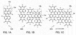
- FIGS. 1A through 1C are views for describing an example of a graphene nanoribbon.
- FIG. 1A illustrates an example of a precursor molecule of a graphene nanoribbon.
- FIG.1B indicates an example of a polymer (polymer chain) of the precursor molecule.
- FIG. 1C illustrates an example of a graphene nanoribbon.
- a precursor molecule 10A having a structure illustrated in FIG. 1A is used for forming a graphene nanoribbon 30A.
- the precursor molecule 10A illustrated in FIG. 1A has a structure in which X and Q in formula (2) are a bromine atom Br and an NH group respectively and in which the polymerization degree s is 0 and is 1,7-dibromoperylene-3,4:9,10-bis(dicarbimide).
- the above precursor molecule 10A is used and bottom-up synthesis is performed.
- the precursor molecule 10A is vacuum-deposited over a heated catalytic metal substrate.
- a (111) plane, a (110) plane, a (100) plane, or a high index plane, such as a (788) plane, of gold (Au), silver (Ag), copper (Cu), or the like is used as the catalytic metal substrate.
- Au gold
- Au gold
- silver Au
- Cu copper
- an Au (111) plane as an example.
- the Au (111) plane purified in an ultrahigh vacuum is kept at a temperature of about 200 to 300oC and the precursor molecule 10A is vacuum-deposited thereover. At this time it is desirable to control a deposition amount so that about one-molecule layer will be formed.
- the Au (111) plane over which the polymer 20A is formed is heated in a vacuum at a higher temperature of about 350 to 450oC. This high temperature heating causes in the polymer 20A over the Au (111) plane a dehydrogenation reaction by which hydrogen H 2 is separated from precursor molecules 10A, and aromatization progress. As a result, the graphene nanoribbon 30A illustrated in FIG. 1C is formed.
- the graphene nanoribbon 30A has a chiral edge 34 at which two benzene rings of a naphthalene structure part 10a of the precursor molecule 10A and one benzene ring formed by aromatization of precursor molecules 10A are arranged alternately and periodically.
- a dicarbimide structure 10b is bonded to the two benzene rings of the naphthalene structure part 10a.
- the dicarbimide structure 10b is periodically bonded to a carbon atom of the chiral edge 34 via a plurality of (three, in this example) carbon atoms.
- the graphene nanoribbon (GNR) 30A of FIG. 1C having the chiral edge 34 to which the dicarbimide (DCI) structure 10b is bonded may be represented by "(2, 1)-DCI-GNR".
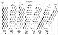
- FIGS. 2A through 2G are views for describing an edge structure of a graphene nanoribbon.
- FIG. 2D illustrates the chiral edge 34 of the graphene nanoribbon 30A illustrated in FIG. 1C .
- FIGS. 2A through 2C and 2E through 2G illustrate an armchair edge 31, other chiral edges 32, 33, 35, and 36, and a zigzag edge 37, respectively, for comparison.
- Angles of the chiral edges 32 through 36 are in the range of 0o, which is the angle of the armchair edge 31, to 30o, which is the angle of the zigzag edge 37.
- the chiral edges 32 through 36 form angles of 4.7o ( FIG. 2B ), 8.9o ( FIG. 2C ), 10.8o ( FIG. 2D ), 13.9o ( FIG. 2E ), and 23.4o ( FIG. 2F ), depending on their shapes.
- the angle of the chiral edge 34 of the graphene nanoribbon 30A ((2, 1)-DCI-GNR) illustrated in FIG. 1C is 10.8o ( FIG. 2D ).
- a band gap of a graphene nanoribbon increases or decreases slightly according to its width. Generally speaking, however, there is the following correlation between an edge angle and a band gap of a graphene nanoribbon.
- a band gap of a graphene nanoribbon decreases as its edge angle increases (see the above "Electronic Structure and Stability of Semiconducting Graphene Nanoribbons").
- Adoption of (2, 1)-DCI-GNR having the chiral edge 34 whose angle is 10.8o realizes a small band gap, compared with the AGNR having the armchair edge 31 and approximately the same width.
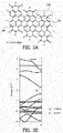
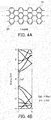
- FIGS. 3A, 3B , 4A, and 4B are views for describing the band structure of a graphene nanoribbon.
- FIG. 3A illustrates the structure of (2, 1)-DCI-GNR and FIG. 3B illustrates a result obtained by estimating its band structure by a density functional method.
- FIG. 4A illustrates the structure of an AGNR (7-AGNR) having width corresponding to seven carbon atoms and FIG. 4B illustrates a result obtained by estimating its band structure by the density functional method.
- the 7-AGNR is formed by forming a polymer chain by polymerization ofanthracene dimers (precursor molecules) to which a halogen atom is bonded and aromatizing the polymer chain after that.
- a band gap Eg2 of the 7-AGNR is estimated to be 1.56 eV. This value is smaller than a value experimentally reported. This is a known problem as the limit of the density functional method in the case of estimating a band gap of a graphene nanoribbon. However, it is possible to correctly estimate a relative magnitude relationship.
- a band gap Eg1 of the (2, 1)-DCI-GNR is estimated by the density functional method to be 0.66 eV. The band gap Eg1 of the (2, 1)-DCI-GNR is smaller than half of the band gap Eg2 of the 7-AGNR.
- a small band gap is realized by the (2, 1)-DCI-GNR having the chiral edge 34 whose angle is 10.8o ( FIG. 2D ), compared with the 7-AGNR having the armchair edge 31 and approximately the same width.
- small width is realized by the (2, 1)-DCI-GNR, compared with an AGNR whose band gap is approximately the same. That is to say, a relatively small precursor molecule may be used in the bottom-up synthesis to obtain a band gap which is approximately the same as that of an AGNR.
- a work function ⁇ 1 of the (2, 1)-DCI-GNR and a work function ⁇ 2 of the 7-AGNR are estimated by the density functional method to be 5.2 eV and 3.7 eV respectively.
- the dicarbimide structure 10b is expected to have the effect of delocalizing and stabilizing radicals and significantly improving the stability of a reaction intermediate, namely the stability of a biradical produced by separating a bromine atom Br from the precursor molecule 10A, in this example.
- FIGS. 5A through 5D are views for describing the stability of a molecule.
- FIGS. 5A through 5D illustrate the stability of radicals at the time of a dicarbimide structure, a fluorine atom F, or a dioxine structure (-OCCO-) being bonded to an anthracene structure part with a radical of the anthracene structure part corresponding to part of a precursor molecule of the 7-AGNR as a reference.
- FIG. 5A illustrates anthracene 40A.
- FIG. 5B illustrates anthracene 40B to which a dicarbimide structure 10b is bonded.
- FIG. 5C illustrates anthracene 40C to which a fluorine atom F is bonded.
- FIG. 5D illustrates anthracene 40D to which a dioxine structure 10d is bonded.
- a radical of the anthracene 40A illustrated in FIG. 5A is considered as a reference (0 eV)
- a radical of the anthracene 40B of FIG. 5B to which the dicarbimide structure 10b is bonded is 2.4 eV more stable than the radical of the anthracene 40A.
- a radical of the anthracene 40C of FIG. 5C to which the fluorine atom F is bonded is 1.4 eV less stable than the radical of the anthracene 40A.
- a radical of the anthracene 40D of FIG. 5D to which the dioxine structure 10d is bonded is 1.3 eV less stable than the radical of the anthracene 40A.
- the above dicarbimide structure 10b of the precursor molecule 10A is expected to have the effect of improving the stability of a reaction intermediate of the precursor molecule 10A.
- the dicarbimide structure 10b contains a nitrogen atom N and an oxygen atom O which are acceptors of a hydrogen bond.
- N nitrogen atom
- O oxygen atom
- the graphene nanoribbon 30A having the above characteristics is excellent in applicability to various semiconductor devices.
- the large precursor molecule needs vacuum deposition at a high temperature for formation and is originally designed so as to have high reactivity. As a result, in many cases, the large precursor molecule decomposes in a deposition process. Therefore, it is not always easy to use a moderately large precursor molecule for obtaining a graphene nanoribbon having large width, a small band gap, and an armchair edge.
- the length of conventional graphene nanoribbons having an armchair edge is about 20 nm on average.
- channel length with a length of about 10 nm, at the most, can be fabricated by the use of the present microfabrication technology. If a contact area between a graphene nanoribbon and an electrode is not wide, then contact resistance increases. Therefore, with the present graphene nanoribbon having an armchair edge, the ribbon length is not always sufficient to ensure fabricable channel length and to ensure a contact area between the graphene nanoribbon and an electrode for making contact resistance low.
- a comparatively small precursor molecule 10A (in which an acene structure part and its polymerization degree are comparatively small) is used in the bottom-up synthesis. Even if such a precursor molecule 10A is used, the graphene nanoribbon 30A having a comparatively small band gap is obtained.
- This graphene nanoribbon 30A is suitable for an FET or the like. As a result, an increase in vacuum deposition temperature at bottom-up synthesis time or decomposition of a precursor molecule in a deposition process is suppressed, compared with a case where a large precursor molecule is used for realizing a small band gap.
- FIGS. 6A through 6C are views for describing another example of a graphene nanoribbon.
- FIG. 6A illustrates another example of a precursor molecule of a graphene nanoribbon.
- FIG.6B indicates another example of a polymer (polymer chain) of the precursor molecule.
- FIG. 6C illustrates another example of a graphene nanoribbon.
- a precursor molecule 10B having a structure illustrated in FIG. 6A is used for forming a graphene nanoribbon 30B.
- the precursor molecule 10B illustrated in FIG. 6A has a structure in which X and Q in formula (2) are a bromine atom Br and an oxygen atom O respectively and in which the polymerization degree s is 0.
- the precursor molecule 10B contains a carboxylic acid anhydride structure 10c. This precursor molecule 10B is used and the bottom-up synthesis is performed.
- the precursor molecule 10B is vacuum-deposited over a catalytic metal substrate, such as an Au (111) plane, purified in an ultrahigh vacuum and kept at a temperature of about 200 to 300oC. At this time a deposition amount is controlled so that about one-molecule layer, for example, will be formed. Polymerization of precursor molecules 10B progresses over the Au (111) plane by a dehydrohalogenation reaction by which hydrogen bromide HBr is separated from adsorbed precursor molecules 10B. As a result, a polymer 20B illustrated in FIG. 6B is formed.
- a catalytic metal substrate such as an Au (111) plane
- the Au (111) plane over which the polymer 20B is formed is heated in a vacuum at a higher temperature of about 350 to 450oC. This high temperature heating causes in the polymer 20B over the Au (111) plane a dehydrogenation reaction by which hydrogen H 2 is separated from precursor molecules 10B, and aromatization progress. As a result, the graphene nanoribbon 30B illustrated in FIG. 6C is formed.
- the graphene nanoribbon 30B illustrated in FIG. 6C has a chiral edge 34 at which two benzene rings of a naphthalene structure part 10a of the precursor molecule 10B and one benzene ring formed by aromatization of precursor molecules 10B are arranged alternately and periodically.
- the carboxylic acid anhydride structure 10c is bonded to the two benzene rings of the naphthalene structure part 10a.
- the carboxylic acid anhydride structure 10c is periodically bonded to a carbon atom of the chiral edge 34 via a plurality of (three, in this example) carbon atoms.
- the angle of the chiral edge 34 of the graphene nanoribbon 30B is 10.8o.
- a small band gap is realized by the graphene nanoribbon 30B, compared with a graphene nanoribbon having an armchair edge and approximately the same width.
- a small width is realized by the (2, 1)-DCI-GNR, compared with an AGNR whose band gap is approximately the same. Therefore, a relatively small precursor molecule 10B may be used in the bottom-up synthesis.
- a work function of the graphene nanoribbon 30B increases due to the electron-withdrawing property of the carboxylic acid anhydride structure 10c. Therefore, n-type operation is easily realized by connecting as an electrode metal whose work function is comparatively low.
- the stability of a reaction intermediate is improved by the electron-withdrawing property of the carboxylic acid anhydride structure 10c.
- the ribbon length of the graphene nanoribbon 30B increases and a polymerization defect is corrected.
- the carboxylic acid anhydride structure 10c contains an oxygen atom O which is an acceptor of a hydrogen bond.
- O oxygen atom
- the graphene nanoribbon 30B having the above characteristics is excellent in applicability to various semiconductor devices.
- FIG. 7 illustrates a first example of a semiconductor device.
- FIG. 7 schematically illustrates a sectional view of the semiconductor device.
- a semiconductor device 50 illustrated in FIG. 7 is an example of a bottom gate type FET.
- the semiconductor device 50 includes a gate electrode 51, a gate insulating film 52, a graphene nanoribbon 53, an electrode 54a, and an electrode 54b.
- a conductive substrate is used as the gate electrode 51.
- a semiconductor substrate such as a silicon (Si) substrate, doped with an impurity element of a determined conduction type is used.
- the gate insulating film 52 is formed over this gate electrode 51.
- the graphene nanoribbon according to the above first embodiment represented by formula (1) and having the chiral edge or the graphene nanoribbon 30A or 30B according to the above second or third embodiment having the chiral edge 34 is used as the graphene nanoribbon 53.
- the graphene nanoribbon 53 is formed by transferring the graphene nanoribbon formed by the bottom-up synthesis described in the above first, second, or third embodiment over the gate insulating film 52 over the gate electrode 51.
- the electrode 54a and the electrode 54b are formed over one end portion and the other end portion, respectively, of the graphene nanoribbon 53 formed over the gate insulating film 52.
- the electrode 54a and the electrode 54b are formed by the use of metal such as Ti, chromium (Cr), cobalt (Co), nickel (Ni), palladium (Pd), aluminum (Al), Cu, Ag, platinum (Pt), or Au.
- the graphene nanoribbon 53 is used as a channel.
- An on state and an off state of the graphene nanoribbon 53 which connects the electrode 54a and the electrode 54b, that is to say, of the channel are controlled by controlling the potential of the gate electrode 51.
- a high-speed FET is realized by making use of high carrier mobility of the graphene nanoribbon 53.
- a graphene nanoribbon having a chiral edge and a band gap suitable for an FET is used as the graphene nanoribbon 53 of the semiconductor device 50.
- An electron-withdrawing group bonded to the chiral edge enables n-type operation of the graphene nanoribbon 53.
- the graphene nanoribbon 53 with proper ribbon length and good orientation in which a polymerization defect is suppressed is formed over the gate insulating film 52 by the effect of the electron-withdrawing group.
- a high performance semiconductor device 50 using the graphene nanoribbon 53 having the chiral edge to which the electron-withdrawing group is bonded is realized.
- the resistance of the graphene nanoribbon 53 changes at the time of adsorbing a molecule.
- the semiconductor device 50 illustrated in FIG. 7 may also be used as an FET-type gas sensor by utilizing this property of the graphene nanoribbon 53. With the semiconductor device 50 used as the FET-type gas sensor, a change in the relationship at the time of the graphene nanoribbon 53 adsorbing a gas between a current flowing between the electrode 54a and the electrode 54b and a voltage of the gate electrode 51 is measured. An FET-type gas sensor having high sensitivity is realized by the use of the graphene nanoribbon 53.
- FIG. 8 illustrates a second example of a semiconductor device.
- FIG. 8 schematically illustrates a sectional view of the semiconductor device.
- a semiconductor device 60 illustrated in FIG. 8 is an example of a top gate type FET.
- the semiconductor device 60 includes a support substrate 61, a graphene nanoribbon 62, an electrode 63a, an electrode 63b, a gate insulating film 64, and a gate electrode 65.
- An insulating substrate such as a sapphire substrate, is used as the support substrate 61.
- a substrate at least whose surface layer is formed by the use of an inorganic or organic insulating material is used as the support substrate 61.
- the graphene nanoribbon 62 is formed over the support substrate 61.
- the graphene nanoribbon according to the above first embodiment represented by formula (1) and having the chiral edge or the graphene nanoribbon 30A or 30B according to the above second or third embodiment having the chiral edge 34 is used as the graphene nanoribbon 62.
- the graphene nanoribbon 62 is formed by transferring over the support substrate 61 the graphene nanoribbon formed by the bottom-up synthesis described in the above first, second, or third embodiment.
- the electrode 63a and the electrode 63b are formed over one end portion and the other end portion, respectively, of the graphene nanoribbon 62 formed over the support substrate 61.
- the electrode 63a and the electrode 63b are formed by the use of metal such as Ti, Cr, Co, Ni, Pd, Al, Cu, Ag, Pt, or Au.
- the gate electrode 65 is formed over the graphene nanoribbon 62 between the electrode 63a and electrode 63b with the gate insulating film 64 therebetween.
- the gate insulating film 64 is formed by the use of an insulating material such as SiO.
- the gate electrode 65 is formed by the use of polycrystalline silicon or a conductor material such as metal.
- the graphene nanoribbon 62 is used as a channel.
- An on state and an off state of the graphene nanoribbon 62 which connects the electrode 63a and the electrode 63b, that is to say, of the channel are controlled by controlling the potential of the gate electrode 65.
- a high-speed FET is realized by making use of high carrier mobility of the graphene nanoribbon 62.
- a graphene nanoribbon having a chiral edge and a band gap suitable for an FET is used as the graphene nanoribbon 62 of the semiconductor device 60.
- An electron-withdrawing group bonded to the chiral edge enables n-type operation of the graphene nanoribbon 62.
- the graphene nanoribbon 62 with proper ribbon length and good orientation in which a polymerization defect is suppressed is formed over the support substrate 61 by the effect of the electron-withdrawing group.
- a high performance semiconductor device 60 using the graphene nanoribbon 62 having the chiral edge to which the electron-withdrawing group is bonded is realized.
- FIG. 9 illustrates a third example of a semiconductor device.
- FIG. 9 schematically illustrates a sectional view of the semiconductor device.
- a semiconductor device 70 illustrated in FIG. 9 is an example of a Schottky barrier diode.
- the semiconductor device 70 includes a support substrate 71, a graphene nanoribbon 72, an electrode 73, and an electrode 74.
- An insulating substrate such as a sapphire substrate, is used as the support substrate 71.
- a substrate at least whose surface layer is formed by the use of an inorganic or organic insulating material is used as the support substrate 71.
- the graphene nanoribbon 72 is formed over the support substrate 71.
- the graphene nanoribbon according to the above first embodiment represented by formula (1) and having the chiral edge or the graphene nanoribbon 30A or 30B according to the above second or third embodiment having the chiral edge 34 is used as the graphene nanoribbon 72.
- the graphene nanoribbon 72 is formed by transferring over the support substrate 71 the graphene nanoribbon formed by the bottom-up synthesis described in the above first, second, or third embodiment.
- the electrode 73 and the electrode 74 are formed over one end portion and the other end portion, respectively, of the graphene nanoribbon 72 formed over the support substrate 71.
- the electrode 73 is formed by the use of metal, such as Cr, which forms a Schottky connection with the graphene nanoribbon 72.
- the electrode 74 is formed by the use of metal, such as Ti, which forms an ohmic connection with the graphene nanoribbon 72.
- a graphene nanoribbon having a chiral edge and a band gap suitable for a Schottky barrier diode is used as the graphene nanoribbon 72 of the semiconductor device 70.
- An electron-withdrawing group bonded to the chiral edge enables n-type operation of the graphene nanoribbon 72.
- the graphene nanoribbon 72 with proper ribbon length and good orientation in which a polymerization defect is suppressed is formed over the support substrate 71 by the effect of the electron-withdrawing group.
- the graphene nanoribbon 72 having the chiral edge to which the electron-withdrawing group is bonded is used, a Schottky connection with the electrode 73 is realized on the one end portion side, and an ohmic connection with the electrode 74 is realized on the other end portion side.
- a Schottky barrier diode having excellent diode characteristics is realized.
- the above graphene nanoribbon 53, 62, or 72 may be formed over a material having the function of doping it, for example, over what is called a self-assembled monolayer (SAM).
- SAM self-assembled monolayer
- a graphene nanoribbon obtained by connecting graphene nanoribbons of different widths each having a chiral edge to which an electron-withdrawing group is bonded may be used as the above graphene nanoribbon 53, 62, or 72.
- a graphene nanoribbon obtained by connecting a graphene nanoribbon having a chiral edge to which an electron-withdrawing group is bonded and a graphene nanoribbon having an armchair edge or a graphene nanoribbon whose edge is terminated with a functional group may be used as the above graphene nanoribbon 53, 62, or 72. In any of these cases, parts which differ in band gap or work function are formed in the graphene nanoribbon 53, 62, or 72.
- electrodes 63a and 63b, or electrodes 73 and 74 for example, contact resistance or barrier height is controlled by the use of the graphene nanoribbon 53, 62, or 72 including these parts.
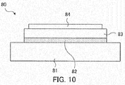
- FIG. 10 illustrates a fourth example of a semiconductor device.
- FIG. 10 schematically illustrates a sectional view of the semiconductor device.
- a semiconductor device 80 illustrated in FIG. 10 is an example of a laminated solar cell.
- the semiconductor device 80 includes a lower electrode 81, a graphene nanoribbon 82, a carrier transport layer 83, and an upper electrode 84.
- the lower electrode 81 and the upper electrode 84 are formed by the use of a transparent conductor material such as indium tin oxide.
- a transparent conductor material such as indium tin oxide.
- one (lower electrode 81, for example) of the lower electrode 81 and the upper electrode 84 is formed by the use of a transparent conductor material and the other (upper electrode 84, for example) of the lower electrode 81 and the upper electrode 84 is formed by the use of an opaque conductor material such as metal.
- a quantum dot structure laminate or an organic semiconductor material laminate including a pn junction is used as the carrier transport layer 83 formed between the lower electrode 81 and the upper electrode 84.
- the graphene nanoribbon 82 is formed between the lower electrode 81 and the carrier transport layer 83.
- the graphene nanoribbon according to the above first embodiment represented by formula (1) and having the chiral edge or the graphene nanoribbon 30A or 30B according to the above second or third embodiment having the chiral edge 34 is used as the graphene nanoribbon 82.
- the semiconductor device 80 electricity is generated as electrons and holes produced in response to incident light at a pn junction interface in the carrier transport layer 83 reach, for example, the lower electrode 81 and the upper electrode 84 respectively.
- the graphene nanoribbon 82 formed between the carrier transport layer 83 and the lower electrode 81 improves the efficiency of extracting electrons to the lower electrode 81 or controls the work function of the lower electrode 81.
- the graphene nanoribbon 82, together with the lower electrode 81 may be used as part of a lower electrode of a laminated solar cell.
- a graphene nanoribbon having a chiral edge and a work function suitable for a laminated solar cell is used as the graphene nanoribbon 82 of the semiconductor device 80.
- An electron-withdrawing group bonded to the chiral edge enables n-type operation of the graphene nanoribbon 82.
- the graphene nanoribbon 82 with proper ribbon length and good orientation in which a polymerization defect is suppressed is formed between the lower electrode 81 and the carrier transport layer 83 by the effect of the electron-withdrawing group.
- a graphene nanoribbon which improves the efficiency of extracting holes to the upper electrode 84 or which controls the work function of the upper electrode 84 may be formed between the carrier transport layer 83 and the upper electrode 84. Furthermore, the graphene nanoribbon, together with the upper electrode 84, may be used as part of an upper electrode of a laminated solar cell.
- Various electronic devices may be equipped with the semiconductor devices 50, 60, 70, 80, and the like according to the above fourth embodiment.
- the semiconductor devices 50, 60, 70, 80, and the like may be used in various electronic devices such as computers (personal computers, supercomputers, servers, and the like), smartphones, portable telephones, tablet terminals, sensors, cameras, audio equipment, measuring equipment, inspection equipment, and manufacturing equipment.
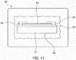
- FIG. 11 is a view for describing an electronic device.
- FIG. 11 is a schematic view of an example of the electronic device.
- the semiconductor device 50 illustrated in FIG. 7 is carried by (incorporated in) an electronic device 90.
- the semiconductor device 50 as stated above, the graphene nanoribbon 53 having a chiral edge to which an electron-withdrawing group is bonded is used. Characteristics, such as a band gap, a work function, ribbon length, orientation, and contact resistance, needed for the graphene nanoribbon 53 of the semiconductor device 50 are satisfied by the chiral edge and the electron-withdrawing group bonded thereto.
- a high performance semiconductor device 50 using the graphene nanoribbon 53 is realized and a high performance electronic device 90 which carries such a semiconductor device 50 is realized.
- the semiconductor device 50 illustrated in FIG. 7 is taken as an example. However, the other semiconductor devices 60, 70, 80, and the like are also carried by various electronic devices.
- a graphene nanoribbon excellent in applicability to a semiconductor device is realized. Furthermore, a high performance semiconductor device using such a graphene nanoribbon is realized.
Landscapes
- Chemical & Material Sciences (AREA)
- Engineering & Computer Science (AREA)
- Nanotechnology (AREA)
- Organic Chemistry (AREA)
- Materials Engineering (AREA)
- Physics & Mathematics (AREA)
- Condensed Matter Physics & Semiconductors (AREA)
- General Physics & Mathematics (AREA)
- Crystallography & Structural Chemistry (AREA)
- Chemical Kinetics & Catalysis (AREA)
- Health & Medical Sciences (AREA)
- Medicinal Chemistry (AREA)
- Polymers & Plastics (AREA)
- Composite Materials (AREA)
- Manufacturing & Machinery (AREA)
- Inorganic Chemistry (AREA)
- Carbon And Carbon Compounds (AREA)
- Thin Film Transistor (AREA)
- Physical Deposition Of Substances That Are Components Of Semiconductor Devices (AREA)
- Electroluminescent Light Sources (AREA)
- Physical Vapour Deposition (AREA)
- Chemical Vapour Deposition (AREA)
- Electrodes Of Semiconductors (AREA)
Abstract
Description
- The embodiments discussed herein are related to a graphene nanoribbon, a graphene nanoribbon fabrication method, and a semiconductor device.
- A graphene nanoribbon is known as one of nanocarbon materials. In view of application of a graphene nanoribbon to semiconductor devices such as field effect transistors, there is an attempt to control its width and edge structure so as to obtain a semiconducting graphene nanoribbon having a band gap. For example, an armchair edge or a chiral edge is known as an edge structure of a semiconducting graphene nanoribbon.
- See, for example, the following documents:
- International Publication Pamphlet No.
WO2013/061258 ; and - Veronica Barone, Oded Hod, and Gustavo E. Scuseria, "Electronic Structure and Stability of Semiconducting Graphene Nanoribbons", Nano Letters, Vol. 6, No. 12, pp. 2748-2754, 2006.
- Applying a graphene nanoribbon to a semiconductor device does not always result in a high performance semiconductor device. The reason for this is that it is difficult to obtain a graphene nanoribbon having a shape and characteristics, such as a band gap, suitable for the semiconductor device.
- According to an aspect, there is provided a graphene nanoribbon having a chiral edge to which an electron-withdrawing group is bonded.
- The invention is described, by way of example only, with reference to the following drawings, in which:
-
FIGS. 1A through 1C are views for describing an example of a graphene nanoribbon; -
FIGS. 2A through 2G are views for describing an edge structure of a graphene nanoribbon; -
FIGS. 3A and 3B are views for describing the band structure of a graphene nanoribbon (part 1) ; -
FIGS. 4A and 4B are views for describing the band structure of a graphene nanoribbon (part 2); -
FIGS. 5A through 5D are views for describing the stability of a molecule; -
FIGS. 6A through 6C are views for describing another example of a graphene nanoribbon; -
FIG. 7 illustrates a first example of a semiconductor device; -
FIG. 8 illustrates a second example of a semiconductor device; -
FIG. 9 illustrates a third example of a semiconductor device; -
FIG. 10 illustrates a fourth example of a semiconductor device; and -
FIG. 11 is a view for describing an electronic device. - A first embodiment will be described.
- A graphene nanoribbon according to a first embodiment has a structure represented by the following formula (1),

- The edges (edges opposite each other in the width direction) of the graphene nanoribbon represented by formula (1) are chiral edges. Furthermore, an imide structure (dicarbimide structure (-CONRCO-)) or an acid anhydride structure (carboxylic acid anhydride structure (-COOCO-)) is bonded to the chiral edges of the graphene nanoribbon.
- The graphene nanoribbon represented by formula
- (1) is formed by, for example, a bottom-up method (bottom-up synthesis). That is to say, the graphene nanoribbon represented by formula (1) is synthesized by polymerizing precursor molecules represented by the following formula (2)

- The precursor molecule represented by formula (2) has the following molecular structure. A plurality of naphthalene structure parts each containing a group of benzene rings arranged in a horizontal direction (first direction) is polymerized in a vertical direction (second direction). A halogen atom x and an electron-withdrawing group (an imide structure or an acid anhydride structure) are bonded to determined carbon sites of terminal naphthalene structure parts. A halogen atom is bonded to 3-position and 7-position carbon atoms (β-position carbon atoms at the edges in the first direction) of the terminal naphthalene structure parts and electron-withdrawing groups are bonded to 1-position and 8-position carbon atoms and 4-position and 5-position carbon atoms (group of α-position carbon atoms at the edges in the second direction) of the terminal naphthalene structure parts.
- An aromatic compound which is represented by formula (2) and in which the halogen atom x and the electron-withdrawing group are bonded to determined carbon sites is used as precursor molecules used for forming the graphene nanoribbon represented by formula (1) by the bottom-up synthesis.
- With the bottom-up synthesis, first precursor molecules represented by formula (2) are deposited over a heated substrate containing a catalytic metal in a vacuum (vacuum deposition). This vacuum deposition is performed at a temperature of, for example, about 200 to 300°C. When the vacuum deposition is performed, a plurality of precursor molecules is polymerized by a dehydrohalogenation (HX) reaction among the precursor molecules deposited over the substrate to form a polymer chain of an aromatic compound. The polymer chain formed by the vacuum deposition is heated further in a vacuum at a higher temperature (high temperature heating). This high temperature heating is performed at a temperature of, for example, about 350 to 450°C. When this high temperature heating is performed, aromatization (cyclization) progresses in the polymer chain of the aromatic compound over the substrate by a dehydrogenation reaction. The graphene nanoribbon represented by formula (1) is formed by the dehydrohalogenation reaction and dehydrogenation reaction of the precursor molecules.
- Usually the width of a graphene nanoribbon has an influence on its band gap. There is a tendency for the band gap of a graphene nanoribbon to become smaller as its width increases. The width of the graphene nanoribbon represented by formula (1) is controlled by the size of the precursor molecule represented by formula (2), that is to say, by a polymerization degree s of naphthalene structure parts. As a result, its band gap is controlled.
- The edges of the graphene nanoribbon represented by formula (1) and formed by the use of the precursor molecule represented by formula (2) are not armchair edges but chiral edges with low symmetry. The small width graphene nanoribbon having such chiral edges realizes a small band gap, compared with a graphene nanoribbon having armchair edges.
- Furthermore, an imide structure or an acid anhydride structure is bonded to the chiral edges of the graphene nanoribbon represented by formula (1) and formed by the use of the precursor molecule represented by formula (2). Both of the imide structure or the acid anhydride structure function as electron-withdrawing groups. As a result, with the graphene nanoribbon having the chiral edges, the position of a conduction band is energetically deep, compared with a graphene nanoribbon having armchair edges. As a result, a work function increases. This enables n-type operation of the graphene nanoribbon by connecting as an electrode metal, such as titanium (Ti), whose work function is comparatively low.
- It is expected that an electron-withdrawing group has the resonance effect of delocalizing and stabilizing radicals. This improves the stability (lifetime) of a reaction intermediate. The reaction intermediate is a biradical produced by separating the halogen atom X from the precursor molecule. If reaction intermediates are stabilized, the diffusion length of precursor molecules (reaction intermediates) over the substrate increases and the polymerization degree t increases. Therefore, it is expected that the ribbon length of the graphene nanoribbon increases.
- Furthermore, if reaction intermediates are stabilized, a bond is easily cleaved from a polymer chain under reaction. As a result, a precursor molecule (reaction intermediate) is easily separated from over the substrate. That is to say, even if precursor molecules are bonded together in an undesirable form and a polymerization defect appears, the possibility that precursor molecules at a defective site are separated and that precursor molecules are bonded together anew in a desirable form at the site increases. A polymerization defect prevents the graphene nanoribbon from lengthening. Therefore, a process for correcting such a polymerization defect is important.
- In addition, an imide structure or an acid anhydride structure which functions as an electron-withdrawing group contains a nitrogen atom N and an oxygen atom O which are acceptors of a hydrogen bond. Therefore, self-organization of adjacent graphene nanoribbons occurs by the hydrogen bond. This improves the orientation of the graphene nanoribbons.
- As has been described, with the small width graphene nanoribbon represented by formula (1) and having chiral edges, a small band gap is realized and n-type operation is realized by an increase in work function caused by an electron-withdrawing group bonded thereto. Furthermore, a graphene nanoribbon with long ribbon length and good orientation in which a polymerization defect is suppressed is realized by the electron-withdrawing group.
- Formula (2) indicates as an example a precursor molecule having a basic structure in which naphthalene structure parts are polymerized. However, another precursor molecule may be used for forming a graphene nanoribbon having chiral edges. A precursor molecule having a basic structure in which acene structure parts, such as anthracene structure parts, tetracene structure parts, or pentacene structure parts, are polymerized may be used for forming a graphene nanoribbon having a chiral edge. In this case, a chiral edge having a periodic structure corresponding to the number of benzene rings contained in a terminal acene structure part of a precursor molecule is formed in a graphene nanoribbon.
- Concrete examples of the above graphene nanoribbon and a precursor molecule used for forming the above graphene nanoribbon will now be described as second and third embodiments.
- First, a second embodiment will be described.
-
FIGS. 1A through 1C are views for describing an example of a graphene nanoribbon.FIG. 1A illustrates an example of a precursor molecule of a graphene nanoribbon.FIG.1B indicates an example of a polymer (polymer chain) of the precursor molecule.FIG. 1C illustrates an example of a graphene nanoribbon. - For example, a
precursor molecule 10A having a structure illustrated inFIG. 1A is used for forming agraphene nanoribbon 30A. Theprecursor molecule 10A illustrated inFIG. 1A has a structure in which X and Q in formula (2) are a bromine atom Br and an NH group respectively and in which the polymerization degree s is 0 and is 1,7-dibromoperylene-3,4:9,10-bis(dicarbimide). Theabove precursor molecule 10A is used and bottom-up synthesis is performed. - With the bottom-up synthesis, first the
precursor molecule 10A is vacuum-deposited over a heated catalytic metal substrate. A (111) plane, a (110) plane, a (100) plane, or a high index plane, such as a (788) plane, of gold (Au), silver (Ag), copper (Cu), or the like is used as the catalytic metal substrate. Description will now be given with an Au (111) plane as an example. The Au (111) plane purified in an ultrahigh vacuum is kept at a temperature of about 200 to 300ºC and theprecursor molecule 10A is vacuum-deposited thereover. At this time it is desirable to control a deposition amount so that about one-molecule layer will be formed. Polymerization ofprecursor molecules 10A progresses over the Au (111) plane by a dehydrohalogenation reaction by which hydrogen bromide HBr is separated from adsorbedprecursor molecules 10A. As a result, apolymer 20A illustrated inFIG. 1B is formed. - After the above vacuum deposition, the Au (111) plane over which the
polymer 20A is formed is heated in a vacuum at a higher temperature of about 350 to 450ºC. This high temperature heating causes in thepolymer 20A over the Au (111) plane a dehydrogenation reaction by which hydrogen H2 is separated fromprecursor molecules 10A, and aromatization progress. As a result, thegraphene nanoribbon 30A illustrated inFIG. 1C is formed. - The
graphene nanoribbon 30A has achiral edge 34 at which two benzene rings of anaphthalene structure part 10a of theprecursor molecule 10A and one benzene ring formed by aromatization ofprecursor molecules 10A are arranged alternately and periodically. Adicarbimide structure 10b is bonded to the two benzene rings of thenaphthalene structure part 10a. Thedicarbimide structure 10b is periodically bonded to a carbon atom of thechiral edge 34 via a plurality of (three, in this example) carbon atoms. In the following description the graphene nanoribbon (GNR) 30A ofFIG. 1C having thechiral edge 34 to which the dicarbimide (DCI)structure 10b is bonded may be represented by "(2, 1)-DCI-GNR". -
FIGS. 2A through 2G are views for describing an edge structure of a graphene nanoribbon. -
FIG. 2D illustrates thechiral edge 34 of thegraphene nanoribbon 30A illustrated inFIG. 1C . In addition,FIGS. 2A through 2C and 2E through 2G illustrate anarmchair edge 31, otherchiral edges zigzag edge 37, respectively, for comparison. - It is assumed that an angle of the
armchair edge 31 of a graphene nanoribbon (AGNR) is 0º (FIG. 2A ). Then an angle of thezigzag edge 37 of a graphene nanoribbon (ZGNR) is 30º (FIG. 2G ). - Angles of the
chiral edges 32 through 36 are in the range of 0º, which is the angle of thearmchair edge 31, to 30º, which is the angle of thezigzag edge 37. As illustrated inFIGS. 2B through 2F , thechiral edges 32 through 36 form angles of 4.7º (FIG. 2B ), 8.9º (FIG. 2C ), 10.8º (FIG. 2D ), 13.9º (FIG. 2E ), and 23.4º (FIG. 2F ), depending on their shapes. The angle of thechiral edge 34 of thegraphene nanoribbon 30A ((2, 1)-DCI-GNR) illustrated inFIG. 1C is 10.8º (FIG. 2D ). - A band gap of a graphene nanoribbon increases or decreases slightly according to its width. Generally speaking, however, there is the following correlation between an edge angle and a band gap of a graphene nanoribbon. A band gap of a graphene nanoribbon decreases as its edge angle increases (see the above "Electronic Structure and Stability of Semiconducting Graphene Nanoribbons"). Adoption of (2, 1)-DCI-GNR having the
chiral edge 34 whose angle is 10.8º realizes a small band gap, compared with the AGNR having thearmchair edge 31 and approximately the same width. -
FIGS. 3A, 3B ,4A, and 4B are views for describing the band structure of a graphene nanoribbon. -
FIG. 3A illustrates the structure of (2, 1)-DCI-GNR andFIG. 3B illustrates a result obtained by estimating its band structure by a density functional method. For comparison,FIG. 4A illustrates the structure of an AGNR (7-AGNR) having width corresponding to seven carbon atoms andFIG. 4B illustrates a result obtained by estimating its band structure by the density functional method. - For example, the 7-AGNR is formed by forming a polymer chain by polymerization ofanthracene dimers (precursor molecules) to which a halogen atom is bonded and aromatizing the polymer chain after that.
- In
FIGS. 4A and 4B , a band gap Eg2 of the 7-AGNR is estimated to be 1.56 eV. This value is smaller than a value experimentally reported. This is a known problem as the limit of the density functional method in the case of estimating a band gap of a graphene nanoribbon. However, it is possible to correctly estimate a relative magnitude relationship. InFIGS. 3A and 3B , a band gap Eg1 of the (2, 1)-DCI-GNR is estimated by the density functional method to be 0.66 eV. The band gap Eg1 of the (2, 1)-DCI-GNR is smaller than half of the band gap Eg2 of the 7-AGNR. - As has been described, a small band gap is realized by the (2, 1)-DCI-GNR having the
chiral edge 34 whose angle is 10.8º (FIG. 2D ), compared with the 7-AGNR having thearmchair edge 31 and approximately the same width. Alternatively, small width is realized by the (2, 1)-DCI-GNR, compared with an AGNR whose band gap is approximately the same. That is to say, a relatively small precursor molecule may be used in the bottom-up synthesis to obtain a band gap which is approximately the same as that of an AGNR. - Furthermore, a work function Φ1 of the (2, 1)-DCI-GNR and a work function Φ2 of the 7-AGNR are estimated by the density functional method to be 5.2 eV and 3.7 eV respectively. This means that the position of a conduction band of the (2, 1)-DCI-GNR is energetically deep due to the electron-withdrawing property of the
dicarbimide structure 10b. Therefore, it is possible to easily realize n-type operation of the (2, 1)-DCI-GNR by connecting as an electrode metal whose work function is comparatively low. - The
dicarbimide structure 10b is expected to have the effect of delocalizing and stabilizing radicals and significantly improving the stability of a reaction intermediate, namely the stability of a biradical produced by separating a bromine atom Br from theprecursor molecule 10A, in this example. -
FIGS. 5A through 5D are views for describing the stability of a molecule.FIGS. 5A through 5D illustrate the stability of radicals at the time of a dicarbimide structure, a fluorine atom F, or a dioxine structure (-OCCO-) being bonded to an anthracene structure part with a radical of the anthracene structure part corresponding to part of a precursor molecule of the 7-AGNR as a reference. -
FIG. 5A illustratesanthracene 40A.FIG. 5B illustratesanthracene 40B to which adicarbimide structure 10b is bonded.FIG. 5C illustratesanthracene 40C to which a fluorine atom F is bonded.FIG. 5D illustratesanthracene 40D to which adioxine structure 10d is bonded. - If a radical of the
anthracene 40A illustrated inFIG. 5A is considered as a reference (0 eV), then a radical of theanthracene 40B ofFIG. 5B to which thedicarbimide structure 10b is bonded is 2.4 eV more stable than the radical of theanthracene 40A. - On the other hand, a radical of the
anthracene 40C ofFIG. 5C to which the fluorine atom F is bonded is 1.4 eV less stable than the radical of theanthracene 40A. A radical of theanthracene 40D ofFIG. 5D to which thedioxine structure 10d is bonded is 1.3 eV less stable than the radical of theanthracene 40A. - From these factors, the
above dicarbimide structure 10b of theprecursor molecule 10A is expected to have the effect of improving the stability of a reaction intermediate of theprecursor molecule 10A. - Because a reaction intermediate of the
precursor molecule 10A is stabilized by thedicarbimide structure 10b, the diffusion length of reaction intermediates over a substrate increases. As a result, the ribbon length of thegraphene nanoribbon 30A is increased. - Furthermore, because a reaction intermediate of the
precursor molecule 10A is stabilized by thedicarbimide structure 10b, there is a high possibility that the reaction intermediate is separated from thepolymer 20A and that a polymerization defect is corrected by its repolymerization to thepolymer 20A. This suppresses a polymerization defect of thegraphene nanoribbon 30A and therefore increases its ribbon length. - In addition, the
dicarbimide structure 10b contains a nitrogen atom N and an oxygen atom O which are acceptors of a hydrogen bond. As a result, self-organization ofadjacent graphene nanoribbons 30A occurs by a hydrogen bond. This improves the orientation of thegraphene nanoribbons 30A. - As has been described, with the small
width graphene nanoribbon 30A having thechiral edge 34, a small bang gap is realized. Also, n-type operation is realized by the electron-withdrawing property of thedicarbimide structure 10b. Furthermore, thegraphene nanoribbon 30A with long ribbon length and good orientation in which a polymerization defect is suppressed is realized by thedicarbimide structure 10b. - The
graphene nanoribbon 30A having the above characteristics is excellent in applicability to various semiconductor devices. - With a graphene nanoribbon having an armchair edge, it is easy to realize a comparatively large band gap. Therefore, if it is applied to, for example, a photoelectric conversion device, it is a good material. On the other hand, however, if it is applied to a field effect transistor (FET), it is difficult due to an excessively large band gap to obtain good bonding with an electrode. A band gap of a graphene nanoribbon tends to become smaller as its width increases. Therefore, in principle, a precursor molecule (its acene structure part) used in the bottom-up synthesis is made large to form a graphene nanoribbon with large width having an armchair edge. However, the large precursor molecule needs vacuum deposition at a high temperature for formation and is originally designed so as to have high reactivity. As a result, in many cases, the large precursor molecule decomposes in a deposition process. Therefore, it is not always easy to use a moderately large precursor molecule for obtaining a graphene nanoribbon having large width, a small band gap, and an armchair edge.
- Furthermore, the length of conventional graphene nanoribbons having an armchair edge is about 20 nm on average. With an FET in which a graphene nanoribbon connects a source electrode and a drain electrode, channel length with a length of about 10 nm, at the most, can be fabricated by the use of the present microfabrication technology. If a contact area between a graphene nanoribbon and an electrode is not wide, then contact resistance increases. Therefore, with the present graphene nanoribbon having an armchair edge, the ribbon length is not always sufficient to ensure fabricable channel length and to ensure a contact area between the graphene nanoribbon and an electrode for making contact resistance low. In addition, if such a comparatively short graphene nanoribbon having an armchair edge grows with random orientation, it is difficult to fabricate FETs in which a graphene nanoribbon connects a source electrode and a drain electrode with a high yield. The orientation of a graphene nanoribbon is controllable by the use of a single crystal having a high index plane. However, this may lead to a significant increase in the costs.
- In the second embodiment, on the other hand, a comparatively
small precursor molecule 10A (in which an acene structure part and its polymerization degree are comparatively small) is used in the bottom-up synthesis. Even if such aprecursor molecule 10A is used, thegraphene nanoribbon 30A having a comparatively small band gap is obtained. Thisgraphene nanoribbon 30A is suitable for an FET or the like. As a result, an increase in vacuum deposition temperature at bottom-up synthesis time or decomposition of a precursor molecule in a deposition process is suppressed, compared with a case where a large precursor molecule is used for realizing a small band gap. Furthermore, it is possible to stably obtain by the bottom-up synthesis thegraphene nanoribbon 30A with comparatively long ribbon length and good orientation which is capable of n-type operation, while suppressing a polymerization defect. This makes it possible to fabricate high performance semiconductor devices, such as FETs, using thegraphene nanoribbon 30A with a high yield, while suppressing an increase in the costs. - A third embodiment will now be described.
-
FIGS. 6A through 6C are views for describing another example of a graphene nanoribbon.FIG. 6A illustrates another example of a precursor molecule of a graphene nanoribbon.FIG.6B indicates another example of a polymer (polymer chain) of the precursor molecule.FIG. 6C illustrates another example of a graphene nanoribbon. - In this case, for example, a
precursor molecule 10B having a structure illustrated inFIG. 6A is used for forming agraphene nanoribbon 30B. Theprecursor molecule 10B illustrated inFIG. 6A has a structure in which X and Q in formula (2) are a bromine atom Br and an oxygen atom O respectively and in which the polymerization degree s is 0. Theprecursor molecule 10B contains a carboxylicacid anhydride structure 10c. Thisprecursor molecule 10B is used and the bottom-up synthesis is performed. - With the bottom-up synthesis, the
precursor molecule 10B is vacuum-deposited over a catalytic metal substrate, such as an Au (111) plane, purified in an ultrahigh vacuum and kept at a temperature of about 200 to 300ºC. At this time a deposition amount is controlled so that about one-molecule layer, for example, will be formed. Polymerization ofprecursor molecules 10B progresses over the Au (111) plane by a dehydrohalogenation reaction by which hydrogen bromide HBr is separated from adsorbedprecursor molecules 10B. As a result, apolymer 20B illustrated inFIG. 6B is formed. - After the above vacuum deposition, the Au (111) plane over which the
polymer 20B is formed is heated in a vacuum at a higher temperature of about 350 to 450ºC. This high temperature heating causes in thepolymer 20B over the Au (111) plane a dehydrogenation reaction by which hydrogen H2 is separated fromprecursor molecules 10B, and aromatization progress. As a result, thegraphene nanoribbon 30B illustrated inFIG. 6C is formed. - The
graphene nanoribbon 30B illustrated inFIG. 6C has achiral edge 34 at which two benzene rings of anaphthalene structure part 10a of theprecursor molecule 10B and one benzene ring formed by aromatization ofprecursor molecules 10B are arranged alternately and periodically. The carboxylicacid anhydride structure 10c is bonded to the two benzene rings of thenaphthalene structure part 10a. The carboxylicacid anhydride structure 10c is periodically bonded to a carbon atom of thechiral edge 34 via a plurality of (three, in this example) carbon atoms. The angle of thechiral edge 34 of thegraphene nanoribbon 30B is 10.8º. - A small band gap is realized by the
graphene nanoribbon 30B, compared with a graphene nanoribbon having an armchair edge and approximately the same width. Alternatively, a small width is realized by the (2, 1)-DCI-GNR, compared with an AGNR whose band gap is approximately the same. Therefore, a relativelysmall precursor molecule 10B may be used in the bottom-up synthesis. - Furthermore, a work function of the
graphene nanoribbon 30B increases due to the electron-withdrawing property of the carboxylicacid anhydride structure 10c. Therefore, n-type operation is easily realized by connecting as an electrode metal whose work function is comparatively low. - Furthermore, the stability of a reaction intermediate is improved by the electron-withdrawing property of the carboxylic
acid anhydride structure 10c. As a result, the ribbon length of thegraphene nanoribbon 30B increases and a polymerization defect is corrected. - In addition, the carboxylic
acid anhydride structure 10c contains an oxygen atom O which is an acceptor of a hydrogen bond. As a result, the orientation ofgraphene nanoribbons 30B is improved by self-organization based on a hydrogen bond. - As has been described, with the small
width graphene nanoribbon 30B according to the third embodiment, a small bang gap is realized. Furthermore, n-type operation is realized by the electron-withdrawing property of the carboxylicacid anhydride structure 10c. This is the same with theabove graphene nanoribbon 30A. In addition, thegraphene nanoribbon 30B with long ribbon length and good orientation in which a polymerization defect is suppressed is realized by the carboxylicacid anhydride structure 10c. - The
graphene nanoribbon 30B having the above characteristics is excellent in applicability to various semiconductor devices. - A fourth embodiment will now be described.
- An example in which the graphene nanoribbon according to the above first embodiment represented by formula (1) or the
graphene nanoribbon -
FIG. 7 illustrates a first example of a semiconductor device.FIG. 7 schematically illustrates a sectional view of the semiconductor device. - A
semiconductor device 50 illustrated inFIG. 7 is an example of a bottom gate type FET. Thesemiconductor device 50 includes agate electrode 51, agate insulating film 52, agraphene nanoribbon 53, anelectrode 54a, and anelectrode 54b. - A conductive substrate is used as the
gate electrode 51. For example, a semiconductor substrate, such as a silicon (Si) substrate, doped with an impurity element of a determined conduction type is used. Thegate insulating film 52 is formed over thisgate electrode 51. An insulating material, such as silicon oxide (SiO), is used for forming thegate insulating film 52. - The graphene nanoribbon according to the above first embodiment represented by formula (1) and having the chiral edge or the
graphene nanoribbon chiral edge 34 is used as thegraphene nanoribbon 53. In this case, for example, thegraphene nanoribbon 53 is formed by transferring the graphene nanoribbon formed by the bottom-up synthesis described in the above first, second, or third embodiment over thegate insulating film 52 over thegate electrode 51. - The
electrode 54a and theelectrode 54b are formed over one end portion and the other end portion, respectively, of thegraphene nanoribbon 53 formed over thegate insulating film 52. Theelectrode 54a and theelectrode 54b are formed by the use of metal such as Ti, chromium (Cr), cobalt (Co), nickel (Ni), palladium (Pd), aluminum (Al), Cu, Ag, platinum (Pt), or Au. - With the
semiconductor device 50 which is a bottom gate type FET, thegraphene nanoribbon 53 is used as a channel. An on state and an off state of thegraphene nanoribbon 53 which connects theelectrode 54a and theelectrode 54b, that is to say, of the channel are controlled by controlling the potential of thegate electrode 51. A high-speed FET is realized by making use of high carrier mobility of thegraphene nanoribbon 53. - A graphene nanoribbon having a chiral edge and a band gap suitable for an FET is used as the
graphene nanoribbon 53 of thesemiconductor device 50. An electron-withdrawing group bonded to the chiral edge enables n-type operation of thegraphene nanoribbon 53. Furthermore, thegraphene nanoribbon 53 with proper ribbon length and good orientation in which a polymerization defect is suppressed is formed over thegate insulating film 52 by the effect of the electron-withdrawing group. In addition, it is possible to connect thisgraphene nanoribbon 53 and theelectrode 54a and theelectrode 54b, while ensuring a contact area by the proper ribbon length and suppressing an increase in contact resistance. - A high
performance semiconductor device 50 using thegraphene nanoribbon 53 having the chiral edge to which the electron-withdrawing group is bonded is realized. - The resistance of the
graphene nanoribbon 53 changes at the time of adsorbing a molecule. Thesemiconductor device 50 illustrated inFIG. 7 may also be used as an FET-type gas sensor by utilizing this property of thegraphene nanoribbon 53. With thesemiconductor device 50 used as the FET-type gas sensor, a change in the relationship at the time of thegraphene nanoribbon 53 adsorbing a gas between a current flowing between theelectrode 54a and theelectrode 54b and a voltage of thegate electrode 51 is measured. An FET-type gas sensor having high sensitivity is realized by the use of thegraphene nanoribbon 53. -
FIG. 8 illustrates a second example of a semiconductor device.FIG. 8 schematically illustrates a sectional view of the semiconductor device. - A
semiconductor device 60 illustrated inFIG. 8 is an example of a top gate type FET. Thesemiconductor device 60 includes asupport substrate 61, agraphene nanoribbon 62, anelectrode 63a, anelectrode 63b, agate insulating film 64, and agate electrode 65. - An insulating substrate, such as a sapphire substrate, is used as the
support substrate 61. A substrate at least whose surface layer is formed by the use of an inorganic or organic insulating material is used as thesupport substrate 61. Thegraphene nanoribbon 62 is formed over thesupport substrate 61. - The graphene nanoribbon according to the above first embodiment represented by formula (1) and having the chiral edge or the
graphene nanoribbon chiral edge 34 is used as thegraphene nanoribbon 62. In this case, for example, thegraphene nanoribbon 62 is formed by transferring over thesupport substrate 61 the graphene nanoribbon formed by the bottom-up synthesis described in the above first, second, or third embodiment. - The
electrode 63a and theelectrode 63b are formed over one end portion and the other end portion, respectively, of thegraphene nanoribbon 62 formed over thesupport substrate 61. Theelectrode 63a and theelectrode 63b are formed by the use of metal such as Ti, Cr, Co, Ni, Pd, Al, Cu, Ag, Pt, or Au. - The
gate electrode 65 is formed over thegraphene nanoribbon 62 between theelectrode 63a andelectrode 63b with thegate insulating film 64 therebetween. Thegate insulating film 64 is formed by the use of an insulating material such as SiO. Thegate electrode 65 is formed by the use of polycrystalline silicon or a conductor material such as metal. - With the
semiconductor device 60 which is a top gate type FET, thegraphene nanoribbon 62 is used as a channel. An on state and an off state of thegraphene nanoribbon 62 which connects theelectrode 63a and theelectrode 63b, that is to say, of the channel are controlled by controlling the potential of thegate electrode 65. A high-speed FET is realized by making use of high carrier mobility of thegraphene nanoribbon 62. - A graphene nanoribbon having a chiral edge and a band gap suitable for an FET is used as the
graphene nanoribbon 62 of thesemiconductor device 60. An electron-withdrawing group bonded to the chiral edge enables n-type operation of thegraphene nanoribbon 62. Furthermore, thegraphene nanoribbon 62 with proper ribbon length and good orientation in which a polymerization defect is suppressed is formed over thesupport substrate 61 by the effect of the electron-withdrawing group. In addition, it is possible to connect thisgraphene nanoribbon 62 and theelectrode 63a and theelectrode 63b, while ensuring a contact area by proper ribbon length and suppressing an increase in contact resistance. - A high
performance semiconductor device 60 using thegraphene nanoribbon 62 having the chiral edge to which the electron-withdrawing group is bonded is realized. -
FIG. 9 illustrates a third example of a semiconductor device.FIG. 9 schematically illustrates a sectional view of the semiconductor device. - A
semiconductor device 70 illustrated inFIG. 9 is an example of a Schottky barrier diode. Thesemiconductor device 70 includes asupport substrate 71, agraphene nanoribbon 72, anelectrode 73, and anelectrode 74. - An insulating substrate, such as a sapphire substrate, is used as the
support substrate 71. A substrate at least whose surface layer is formed by the use of an inorganic or organic insulating material is used as thesupport substrate 71. Thegraphene nanoribbon 72 is formed over thesupport substrate 71. - The graphene nanoribbon according to the above first embodiment represented by formula (1) and having the chiral edge or the
graphene nanoribbon chiral edge 34 is used as thegraphene nanoribbon 72. In this case, for example, thegraphene nanoribbon 72 is formed by transferring over thesupport substrate 71 the graphene nanoribbon formed by the bottom-up synthesis described in the above first, second, or third embodiment. - The
electrode 73 and theelectrode 74 are formed over one end portion and the other end portion, respectively, of thegraphene nanoribbon 72 formed over thesupport substrate 71. Theelectrode 73 is formed by the use of metal, such as Cr, which forms a Schottky connection with thegraphene nanoribbon 72. Theelectrode 74 is formed by the use of metal, such as Ti, which forms an ohmic connection with thegraphene nanoribbon 72. - A graphene nanoribbon having a chiral edge and a band gap suitable for a Schottky barrier diode is used as the
graphene nanoribbon 72 of thesemiconductor device 70. An electron-withdrawing group bonded to the chiral edge enables n-type operation of thegraphene nanoribbon 72. Furthermore, thegraphene nanoribbon 72 with proper ribbon length and good orientation in which a polymerization defect is suppressed is formed over thesupport substrate 71 by the effect of the electron-withdrawing group. In addition, it is possible to connect thisgraphene nanoribbon 72 and theelectrode 73 and theelectrode 74, while ensuring a contact area by proper ribbon length and suppressing an increase in contact resistance. - With the
semiconductor device 70, thegraphene nanoribbon 72 having the chiral edge to which the electron-withdrawing group is bonded is used, a Schottky connection with theelectrode 73 is realized on the one end portion side, and an ohmic connection with theelectrode 74 is realized on the other end portion side. As a result, a Schottky barrier diode having excellent diode characteristics is realized. - The
above graphene nanoribbon - A graphene nanoribbon obtained by connecting graphene nanoribbons of different widths each having a chiral edge to which an electron-withdrawing group is bonded may be used as the
above graphene nanoribbon above graphene nanoribbon graphene nanoribbon connected electrodes electrodes electrodes graphene nanoribbon - Furthermore,
FIG. 10 illustrates a fourth example of a semiconductor device.FIG. 10 schematically illustrates a sectional view of the semiconductor device. - A
semiconductor device 80 illustrated inFIG. 10 is an example of a laminated solar cell. Thesemiconductor device 80 includes alower electrode 81, agraphene nanoribbon 82, acarrier transport layer 83, and anupper electrode 84. - The
lower electrode 81 and theupper electrode 84 are formed by the use of a transparent conductor material such as indium tin oxide. Alternatively, one (lower electrode 81, for example) of thelower electrode 81 and theupper electrode 84 is formed by the use of a transparent conductor material and the other (upper electrode 84, for example) of thelower electrode 81 and theupper electrode 84 is formed by the use of an opaque conductor material such as metal. - A quantum dot structure laminate or an organic semiconductor material laminate including a pn junction is used as the
carrier transport layer 83 formed between thelower electrode 81 and theupper electrode 84. For example, thegraphene nanoribbon 82 is formed between thelower electrode 81 and thecarrier transport layer 83. - The graphene nanoribbon according to the above first embodiment represented by formula (1) and having the chiral edge or the
graphene nanoribbon chiral edge 34 is used as thegraphene nanoribbon 82. - In the
semiconductor device 80, electricity is generated as electrons and holes produced in response to incident light at a pn junction interface in thecarrier transport layer 83 reach, for example, thelower electrode 81 and theupper electrode 84 respectively. In this case, thegraphene nanoribbon 82 formed between thecarrier transport layer 83 and thelower electrode 81 improves the efficiency of extracting electrons to thelower electrode 81 or controls the work function of thelower electrode 81. Furthermore, thegraphene nanoribbon 82, together with thelower electrode 81, may be used as part of a lower electrode of a laminated solar cell. - A graphene nanoribbon having a chiral edge and a work function suitable for a laminated solar cell is used as the
graphene nanoribbon 82 of thesemiconductor device 80. An electron-withdrawing group bonded to the chiral edge enables n-type operation of thegraphene nanoribbon 82. Furthermore, thegraphene nanoribbon 82 with proper ribbon length and good orientation in which a polymerization defect is suppressed is formed between thelower electrode 81 and thecarrier transport layer 83 by the effect of the electron-withdrawing group. - A graphene nanoribbon which improves the efficiency of extracting holes to the
upper electrode 84 or which controls the work function of theupper electrode 84 may be formed between thecarrier transport layer 83 and theupper electrode 84. Furthermore, the graphene nanoribbon, together with theupper electrode 84, may be used as part of an upper electrode of a laminated solar cell. - A fifth embodiment will now be described.
- Various electronic devices (electronic equipment or electronic apparatus) may be equipped with the
semiconductor devices semiconductor devices -
FIG. 11 is a view for describing an electronic device.FIG. 11 is a schematic view of an example of the electronic device. - As illustrated in
FIG. 11 , for example, thesemiconductor device 50 illustrated inFIG. 7 is carried by (incorporated in) anelectronic device 90. With thesemiconductor device 50, as stated above, thegraphene nanoribbon 53 having a chiral edge to which an electron-withdrawing group is bonded is used. Characteristics, such as a band gap, a work function, ribbon length, orientation, and contact resistance, needed for thegraphene nanoribbon 53 of thesemiconductor device 50 are satisfied by the chiral edge and the electron-withdrawing group bonded thereto. As a result, a highperformance semiconductor device 50 using thegraphene nanoribbon 53 is realized and a high performanceelectronic device 90 which carries such asemiconductor device 50 is realized. - The
semiconductor device 50 illustrated inFIG. 7 is taken as an example. However, theother semiconductor devices - A graphene nanoribbon excellent in applicability to a semiconductor device is realized. Furthermore, a high performance semiconductor device using such a graphene nanoribbon is realized.
Claims (8)
- A graphene nanoribbon comprising a chiral edge (34) to which an electron-withdrawing group (10b, 10c) is bonded.
- The graphene nanoribbon according to claim 1, wherein the electron-withdrawing group contains an imide structure (10b) bonded to the chiral edge.
- The graphene nanoribbon according to claim 1, wherein the electron-withdrawing group contains an acid anhydride structure (10c) bonded to the chiral edge.
- The graphene nanoribbon according to any of claims 1 to 3, wherein the electron-withdrawing group is periodically bonded to the chiral edge via a plurality of carbon atoms.
- The graphene nanoribbon according to any of claims 1 to 4, wherein when an angle of an armchair edge (31) is 0º, an angle of the chiral edge is 10.8º.
- A graphene nanoribbon fabrication method comprising polymerizing a plurality of precursor molecules (10A) by a dehydrohalogenation reaction (20A, 20B) and a dehydrogenation reaction (30A, 30B), the plurality of precursor molecules each having a molecular structure in which a plurality of acene structure parts (10a) each containing a group of benzene rings arranged in a first direction is polymerized in a second direction perpendicular to the first direction, a halogen atom is bonded to an edge in the first direction of a terminal acene structure part, and an electron-withdrawing group (10b, 10c) is bonded to an edge in the second direction.
- A semiconductor device comprising a graphene nanoribbon (30A, 30B, 53, 62, 72, 82) having a chiral edge (34) to which an electron-withdrawing group (10b, 10c) is bonded.
- A semiconductor device comprising the graphene nanoribbon according to any of claims 1 to 5.
Applications Claiming Priority (1)
| Application Number | Priority Date | Filing Date | Title |
|---|---|---|---|
| JP2017021020A JP6839355B2 (en) | 2017-02-08 | 2017-02-08 | Graphene nanoribbon, graphene nanoribbon manufacturing method and semiconductor device |
Publications (2)
| Publication Number | Publication Date |
|---|---|
| EP3361510A1 true EP3361510A1 (en) | 2018-08-15 |
| EP3361510B1 EP3361510B1 (en) | 2023-06-21 |
Family
ID=61187097
Family Applications (1)
| Application Number | Title | Priority Date | Filing Date |
|---|---|---|---|
| EP18155338.9A Active EP3361510B1 (en) | 2017-02-08 | 2018-02-06 | Graphene nanoribbon and graphene nanoribbon fabrication method |
Country Status (3)
| Country | Link |
|---|---|
| US (1) | US10662282B2 (en) |
| EP (1) | EP3361510B1 (en) |
| JP (1) | JP6839355B2 (en) |
Families Citing this family (1)
| Publication number | Priority date | Publication date | Assignee | Title |
|---|---|---|---|---|
| US11527407B2 (en) | 2020-03-03 | 2022-12-13 | Applied Materials, Inc. | Vapor deposition of carbon-based films |
Citations (6)
| Publication number | Priority date | Publication date | Assignee | Title |
|---|---|---|---|---|
| US20100224998A1 (en) * | 2008-06-26 | 2010-09-09 | Carben Semicon Limited | Integrated Circuit with Ribtan Interconnects |
| US20120197051A1 (en) * | 2009-06-15 | 2012-08-02 | William Marsh Rice University | Graphene nanoribbons prepared from carbon nanotubes via alkalimetal exposure |
| US20120261644A1 (en) * | 2011-04-18 | 2012-10-18 | International Business Machines Corporation | Structure and method of making graphene nanoribbons |
| WO2013061258A1 (en) | 2011-10-26 | 2013-05-02 | Basf Se | Graphene nanoribbon precursors and monomers suitable for preparation thereof |
| US20150057417A1 (en) * | 2011-09-14 | 2015-02-26 | William Marsh Rice Universtiy | Solvent-based methods for production of graphene nanoribbons |
| US20160207776A1 (en) * | 2013-09-04 | 2016-07-21 | Basf Se | Purification process for graphene nanoribbons |
Family Cites Families (3)
| Publication number | Priority date | Publication date | Assignee | Title |
|---|---|---|---|---|
| GB0802912D0 (en) * | 2008-02-15 | 2008-03-26 | Carben Semicon Ltd | Thin-film transistor, carbon-based layer and method of production thereof |
| JP6062321B2 (en) | 2013-06-03 | 2017-01-18 | 東京エレクトロン株式会社 | Organic semiconductor film, manufacturing method thereof, and transistor structure |
| US10329156B2 (en) * | 2015-05-26 | 2019-06-25 | The Royal Institution For The Advancement Of Learning/Mcgill University | Oxygen functionalized graphene nanoflake, a stable and surfactant-free graphene nanoflake nanofluid and method from making same |
-
2017
- 2017-02-08 JP JP2017021020A patent/JP6839355B2/en active Active
-
2018
- 2018-02-06 EP EP18155338.9A patent/EP3361510B1/en active Active
- 2018-02-06 US US15/889,432 patent/US10662282B2/en active Active
Patent Citations (6)
| Publication number | Priority date | Publication date | Assignee | Title |
|---|---|---|---|---|
| US20100224998A1 (en) * | 2008-06-26 | 2010-09-09 | Carben Semicon Limited | Integrated Circuit with Ribtan Interconnects |
| US20120197051A1 (en) * | 2009-06-15 | 2012-08-02 | William Marsh Rice University | Graphene nanoribbons prepared from carbon nanotubes via alkalimetal exposure |
| US20120261644A1 (en) * | 2011-04-18 | 2012-10-18 | International Business Machines Corporation | Structure and method of making graphene nanoribbons |
| US20150057417A1 (en) * | 2011-09-14 | 2015-02-26 | William Marsh Rice Universtiy | Solvent-based methods for production of graphene nanoribbons |
| WO2013061258A1 (en) | 2011-10-26 | 2013-05-02 | Basf Se | Graphene nanoribbon precursors and monomers suitable for preparation thereof |
| US20160207776A1 (en) * | 2013-09-04 | 2016-07-21 | Basf Se | Purification process for graphene nanoribbons |
Non-Patent Citations (1)
| Title |
|---|
| VERONICA BARONE; ODED HOD; GUSTAVO E. SCUSERIA: "Electronic Structure and Stability of Semiconducting Graphene Nanoribbons", NANO LETTERS, vol. 6, no. 12, 2006, pages 2748 - 2754, XP002514233, DOI: doi:10.1021/NL0617033 |
Also Published As
| Publication number | Publication date |
|---|---|
| US10662282B2 (en) | 2020-05-26 |
| EP3361510B1 (en) | 2023-06-21 |
| JP2018127377A (en) | 2018-08-16 |
| US20180223038A1 (en) | 2018-08-09 |
| JP6839355B2 (en) | 2021-03-10 |
Similar Documents
| Publication | Publication Date | Title |
|---|---|---|
| KR100770258B1 (en) | Organic thin film transistor and its manufacturing method | |
| McGarry et al. | Rubrene-based single-crystal organic semiconductors: Synthesis, electronic structure, and charge-transport properties | |
| US9166062B2 (en) | Field effect transistor using graphene | |
| KR101156620B1 (en) | Field effect transistor having graphene channel layer | |
| KR102412965B1 (en) | Electronic device having two dimensional material layer and method of manufacturing the electronic device using inkjet printing | |
| US10090386B2 (en) | Graphene-metal bonding structure, method of manufacturing the same, and semiconductor device having the graphene-metal bonding structure | |
| JP6247636B2 (en) | Organic semiconductor composition and organic transistor | |
| JP6170488B2 (en) | Novel condensed polycyclic aromatic compounds and uses thereof | |
| KR101539837B1 (en) | Organic semiconductor thin film, organic semiconductor device and organic field effect transistor | |
| KR20100066457A (en) | Organic thin film transistor and organic thin film light-emitting transistor | |
| WO2010139386A1 (en) | Process for aligning nanoparticles | |
| JP2021155329A (en) | Graphene nanoribbon, semiconductor device, compound manufacturing method and graphene nanoribbon manufacturing method | |
| KR20120080060A (en) | Organic thin film transistor and method of manufacturing the same and electronic device including the same | |
| US10636539B2 (en) | Compound, compound fabrication method, and graphene nanoribbon fabrication method | |
| EP3361510B1 (en) | Graphene nanoribbon and graphene nanoribbon fabrication method | |
| JP3959530B2 (en) | Vertical organic FET | |
| JP4892810B2 (en) | Field effect transistor | |
| JP4443944B2 (en) | Transistor and manufacturing method thereof | |
| JP5534702B2 (en) | Organic vertical transistor | |
| JP5713431B2 (en) | Field effect transistor | |
| US9718251B2 (en) | Laminate having porous organic semicoductor thin film and chemical sensor comprising same | |
| JP2008140883A (en) | Organic thin film transistor | |
| Cheng et al. | Fabricating photoswitches and field-effect transistors from self-assembled tetra (2-isopropyl-5-methyphenoxy) copper phthalocyanines nanowires | |
| JP2011249715A (en) | Organic fet | |
| JP2007324258A (en) | Method for producing organic thin film transistor |
Legal Events
| Date | Code | Title | Description |
|---|---|---|---|
| PUAI | Public reference made under article 153(3) epc to a published international application that has entered the european phase |
Free format text: ORIGINAL CODE: 0009012 |
|
| STAA | Information on the status of an ep patent application or granted ep patent |
Free format text: STATUS: THE APPLICATION HAS BEEN PUBLISHED |
|
| AK | Designated contracting states |
Kind code of ref document: A1 Designated state(s): AL AT BE BG CH CY CZ DE DK EE ES FI FR GB GR HR HU IE IS IT LI LT LU LV MC MK MT NL NO PL PT RO RS SE SI SK SM TR |
|
| AX | Request for extension of the european patent |
Extension state: BA ME |
|
| STAA | Information on the status of an ep patent application or granted ep patent |
Free format text: STATUS: REQUEST FOR EXAMINATION WAS MADE |
|
| 17P | Request for examination filed |
Effective date: 20180810 |
|
| RBV | Designated contracting states (corrected) |
Designated state(s): AL AT BE BG CH CY CZ DE DK EE ES FI FR GB GR HR HU IE IS IT LI LT LU LV MC MK MT NL NO PL PT RO RS SE SI SK SM TR |
|
| STAA | Information on the status of an ep patent application or granted ep patent |
Free format text: STATUS: EXAMINATION IS IN PROGRESS |
|
| 17Q | First examination report despatched |
Effective date: 20210324 |
|
| REG | Reference to a national code |
Ref country code: DE Ref legal event code: R079 Free format text: PREVIOUS MAIN CLASS: H01L0029160000 Ipc: C08G0061100000 Ref country code: DE Ref legal event code: R079 Ref document number: 602018052022 Country of ref document: DE Free format text: PREVIOUS MAIN CLASS: H01L0029160000 Ipc: C08G0061100000 |
|
| RIC1 | Information provided on ipc code assigned before grant |
Ipc: B82Y 30/00 20110101ALI20221118BHEP Ipc: B82Y 40/00 20110101ALI20221118BHEP Ipc: H01L 29/16 20060101ALI20221118BHEP Ipc: C01B 32/184 20170101ALI20221118BHEP Ipc: C08G 61/10 20060101AFI20221118BHEP |
|
| GRAP | Despatch of communication of intention to grant a patent |
Free format text: ORIGINAL CODE: EPIDOSNIGR1 |
|
| STAA | Information on the status of an ep patent application or granted ep patent |
Free format text: STATUS: GRANT OF PATENT IS INTENDED |
|
| INTG | Intention to grant announced |
Effective date: 20230117 |
|
| GRAS | Grant fee paid |
Free format text: ORIGINAL CODE: EPIDOSNIGR3 |
|
| GRAA | (expected) grant |
Free format text: ORIGINAL CODE: 0009210 |
|
| STAA | Information on the status of an ep patent application or granted ep patent |
Free format text: STATUS: THE PATENT HAS BEEN GRANTED |
|
| AK | Designated contracting states |
Kind code of ref document: B1 Designated state(s): AL AT BE BG CH CY CZ DE DK EE ES FI FR GB GR HR HU IE IS IT LI LT LU LV MC MK MT NL NO PL PT RO RS SE SI SK SM TR |
|
| REG | Reference to a national code |
Ref country code: CH Ref legal event code: EP |
|
| REG | Reference to a national code |
Ref country code: DE Ref legal event code: R096 Ref document number: 602018052022 Country of ref document: DE |
|
| REG | Reference to a national code |
Ref country code: AT Ref legal event code: REF Ref document number: 1580870 Country of ref document: AT Kind code of ref document: T Effective date: 20230715 |
|
| REG | Reference to a national code |
Ref country code: IE Ref legal event code: FG4D |
|
| REG | Reference to a national code |
Ref country code: LT Ref legal event code: MG9D |
|
| REG | Reference to a national code |
Ref country code: NL Ref legal event code: MP Effective date: 20230621 |
|
| PG25 | Lapsed in a contracting state [announced via postgrant information from national office to epo] |
Ref country code: SE Free format text: LAPSE BECAUSE OF FAILURE TO SUBMIT A TRANSLATION OF THE DESCRIPTION OR TO PAY THE FEE WITHIN THE PRESCRIBED TIME-LIMIT Effective date: 20230621 Ref country code: NO Free format text: LAPSE BECAUSE OF FAILURE TO SUBMIT A TRANSLATION OF THE DESCRIPTION OR TO PAY THE FEE WITHIN THE PRESCRIBED TIME-LIMIT Effective date: 20230921 |
|
| REG | Reference to a national code |
Ref country code: AT Ref legal event code: MK05 Ref document number: 1580870 Country of ref document: AT Kind code of ref document: T Effective date: 20230621 |
|
| PG25 | Lapsed in a contracting state [announced via postgrant information from national office to epo] |
Ref country code: RS Free format text: LAPSE BECAUSE OF FAILURE TO SUBMIT A TRANSLATION OF THE DESCRIPTION OR TO PAY THE FEE WITHIN THE PRESCRIBED TIME-LIMIT Effective date: 20230621 Ref country code: NL Free format text: LAPSE BECAUSE OF FAILURE TO SUBMIT A TRANSLATION OF THE DESCRIPTION OR TO PAY THE FEE WITHIN THE PRESCRIBED TIME-LIMIT Effective date: 20230621 Ref country code: LV Free format text: LAPSE BECAUSE OF FAILURE TO SUBMIT A TRANSLATION OF THE DESCRIPTION OR TO PAY THE FEE WITHIN THE PRESCRIBED TIME-LIMIT Effective date: 20230621 Ref country code: LT Free format text: LAPSE BECAUSE OF FAILURE TO SUBMIT A TRANSLATION OF THE DESCRIPTION OR TO PAY THE FEE WITHIN THE PRESCRIBED TIME-LIMIT Effective date: 20230621 Ref country code: HR Free format text: LAPSE BECAUSE OF FAILURE TO SUBMIT A TRANSLATION OF THE DESCRIPTION OR TO PAY THE FEE WITHIN THE PRESCRIBED TIME-LIMIT Effective date: 20230621 Ref country code: GR Free format text: LAPSE BECAUSE OF FAILURE TO SUBMIT A TRANSLATION OF THE DESCRIPTION OR TO PAY THE FEE WITHIN THE PRESCRIBED TIME-LIMIT Effective date: 20230922 |
|
| PG25 | Lapsed in a contracting state [announced via postgrant information from national office to epo] |
Ref country code: FI Free format text: LAPSE BECAUSE OF FAILURE TO SUBMIT A TRANSLATION OF THE DESCRIPTION OR TO PAY THE FEE WITHIN THE PRESCRIBED TIME-LIMIT Effective date: 20230621 |
|
| PG25 | Lapsed in a contracting state [announced via postgrant information from national office to epo] |
Ref country code: SK Free format text: LAPSE BECAUSE OF FAILURE TO SUBMIT A TRANSLATION OF THE DESCRIPTION OR TO PAY THE FEE WITHIN THE PRESCRIBED TIME-LIMIT Effective date: 20230621 |
|
| PG25 | Lapsed in a contracting state [announced via postgrant information from national office to epo] |
Ref country code: ES Free format text: LAPSE BECAUSE OF FAILURE TO SUBMIT A TRANSLATION OF THE DESCRIPTION OR TO PAY THE FEE WITHIN THE PRESCRIBED TIME-LIMIT Effective date: 20230621 |
|
| PG25 | Lapsed in a contracting state [announced via postgrant information from national office to epo] |
Ref country code: IS Free format text: LAPSE BECAUSE OF FAILURE TO SUBMIT A TRANSLATION OF THE DESCRIPTION OR TO PAY THE FEE WITHIN THE PRESCRIBED TIME-LIMIT Effective date: 20231021 |
|
| PG25 | Lapsed in a contracting state [announced via postgrant information from national office to epo] |
Ref country code: ES Free format text: LAPSE BECAUSE OF FAILURE TO SUBMIT A TRANSLATION OF THE DESCRIPTION OR TO PAY THE FEE WITHIN THE PRESCRIBED TIME-LIMIT Effective date: 20230621 Ref country code: EE Free format text: LAPSE BECAUSE OF FAILURE TO SUBMIT A TRANSLATION OF THE DESCRIPTION OR TO PAY THE FEE WITHIN THE PRESCRIBED TIME-LIMIT Effective date: 20230621 Ref country code: CZ Free format text: LAPSE BECAUSE OF FAILURE TO SUBMIT A TRANSLATION OF THE DESCRIPTION OR TO PAY THE FEE WITHIN THE PRESCRIBED TIME-LIMIT Effective date: 20230621 Ref country code: AT Free format text: LAPSE BECAUSE OF FAILURE TO SUBMIT A TRANSLATION OF THE DESCRIPTION OR TO PAY THE FEE WITHIN THE PRESCRIBED TIME-LIMIT Effective date: 20230621 Ref country code: SM Free format text: LAPSE BECAUSE OF FAILURE TO SUBMIT A TRANSLATION OF THE DESCRIPTION OR TO PAY THE FEE WITHIN THE PRESCRIBED TIME-LIMIT Effective date: 20230621 Ref country code: SK Free format text: LAPSE BECAUSE OF FAILURE TO SUBMIT A TRANSLATION OF THE DESCRIPTION OR TO PAY THE FEE WITHIN THE PRESCRIBED TIME-LIMIT Effective date: 20230621 Ref country code: RO Free format text: LAPSE BECAUSE OF FAILURE TO SUBMIT A TRANSLATION OF THE DESCRIPTION OR TO PAY THE FEE WITHIN THE PRESCRIBED TIME-LIMIT Effective date: 20230621 Ref country code: PT Free format text: LAPSE BECAUSE OF FAILURE TO SUBMIT A TRANSLATION OF THE DESCRIPTION OR TO PAY THE FEE WITHIN THE PRESCRIBED TIME-LIMIT Effective date: 20231023 Ref country code: IS Free format text: LAPSE BECAUSE OF FAILURE TO SUBMIT A TRANSLATION OF THE DESCRIPTION OR TO PAY THE FEE WITHIN THE PRESCRIBED TIME-LIMIT Effective date: 20231021 |
|
| PG25 | Lapsed in a contracting state [announced via postgrant information from national office to epo] |
Ref country code: PL Free format text: LAPSE BECAUSE OF FAILURE TO SUBMIT A TRANSLATION OF THE DESCRIPTION OR TO PAY THE FEE WITHIN THE PRESCRIBED TIME-LIMIT Effective date: 20230621 |
|
| REG | Reference to a national code |
Ref country code: DE Ref legal event code: R097 Ref document number: 602018052022 Country of ref document: DE |
|
| PLBE | No opposition filed within time limit |
Free format text: ORIGINAL CODE: 0009261 |
|
| STAA | Information on the status of an ep patent application or granted ep patent |
Free format text: STATUS: NO OPPOSITION FILED WITHIN TIME LIMIT |
|
| PG25 | Lapsed in a contracting state [announced via postgrant information from national office to epo] |
Ref country code: DK Free format text: LAPSE BECAUSE OF FAILURE TO SUBMIT A TRANSLATION OF THE DESCRIPTION OR TO PAY THE FEE WITHIN THE PRESCRIBED TIME-LIMIT Effective date: 20230621 |
|
| PG25 | Lapsed in a contracting state [announced via postgrant information from national office to epo] |
Ref country code: SI Free format text: LAPSE BECAUSE OF FAILURE TO SUBMIT A TRANSLATION OF THE DESCRIPTION OR TO PAY THE FEE WITHIN THE PRESCRIBED TIME-LIMIT Effective date: 20230621 |
|
| 26N | No opposition filed |
Effective date: 20240322 |
|
| PG25 | Lapsed in a contracting state [announced via postgrant information from national office to epo] |
Ref country code: SI Free format text: LAPSE BECAUSE OF FAILURE TO SUBMIT A TRANSLATION OF THE DESCRIPTION OR TO PAY THE FEE WITHIN THE PRESCRIBED TIME-LIMIT Effective date: 20230621 Ref country code: IT Free format text: LAPSE BECAUSE OF FAILURE TO SUBMIT A TRANSLATION OF THE DESCRIPTION OR TO PAY THE FEE WITHIN THE PRESCRIBED TIME-LIMIT Effective date: 20230621 |
|
| PG25 | Lapsed in a contracting state [announced via postgrant information from national office to epo] |
Ref country code: MC Free format text: LAPSE BECAUSE OF FAILURE TO SUBMIT A TRANSLATION OF THE DESCRIPTION OR TO PAY THE FEE WITHIN THE PRESCRIBED TIME-LIMIT Effective date: 20230621 |
|
| REG | Reference to a national code |
Ref country code: CH Ref legal event code: PL |
|
| PG25 | Lapsed in a contracting state [announced via postgrant information from national office to epo] |
Ref country code: LU Free format text: LAPSE BECAUSE OF NON-PAYMENT OF DUE FEES Effective date: 20240206 |
|
| PG25 | Lapsed in a contracting state [announced via postgrant information from national office to epo] |
Ref country code: CH Free format text: LAPSE BECAUSE OF NON-PAYMENT OF DUE FEES Effective date: 20240229 |
|
| PG25 | Lapsed in a contracting state [announced via postgrant information from national office to epo] |
Ref country code: LU Free format text: LAPSE BECAUSE OF NON-PAYMENT OF DUE FEES Effective date: 20240206 Ref country code: CH Free format text: LAPSE BECAUSE OF NON-PAYMENT OF DUE FEES Effective date: 20240229 |
|
| PG25 | Lapsed in a contracting state [announced via postgrant information from national office to epo] |
Ref country code: BG Free format text: LAPSE BECAUSE OF FAILURE TO SUBMIT A TRANSLATION OF THE DESCRIPTION OR TO PAY THE FEE WITHIN THE PRESCRIBED TIME-LIMIT Effective date: 20230621 |
|
| PG25 | Lapsed in a contracting state [announced via postgrant information from national office to epo] |
Ref country code: BG Free format text: LAPSE BECAUSE OF FAILURE TO SUBMIT A TRANSLATION OF THE DESCRIPTION OR TO PAY THE FEE WITHIN THE PRESCRIBED TIME-LIMIT Effective date: 20230621 |
|
| REG | Reference to a national code |
Ref country code: BE Ref legal event code: MM Effective date: 20240229 |
|
| PG25 | Lapsed in a contracting state [announced via postgrant information from national office to epo] |
Ref country code: BE Free format text: LAPSE BECAUSE OF NON-PAYMENT OF DUE FEES Effective date: 20240229 |
|
| PG25 | Lapsed in a contracting state [announced via postgrant information from national office to epo] |
Ref country code: IE Free format text: LAPSE BECAUSE OF NON-PAYMENT OF DUE FEES Effective date: 20240206 |
|
| PG25 | Lapsed in a contracting state [announced via postgrant information from national office to epo] |
Ref country code: IE Free format text: LAPSE BECAUSE OF NON-PAYMENT OF DUE FEES Effective date: 20240206 Ref country code: BE Free format text: LAPSE BECAUSE OF NON-PAYMENT OF DUE FEES Effective date: 20240229 |
|
| PG25 | Lapsed in a contracting state [announced via postgrant information from national office to epo] |
Ref country code: CY Free format text: LAPSE BECAUSE OF FAILURE TO SUBMIT A TRANSLATION OF THE DESCRIPTION OR TO PAY THE FEE WITHIN THE PRESCRIBED TIME-LIMIT; INVALID AB INITIO Effective date: 20180206 |
|
| PG25 | Lapsed in a contracting state [announced via postgrant information from national office to epo] |
Ref country code: HU Free format text: LAPSE BECAUSE OF FAILURE TO SUBMIT A TRANSLATION OF THE DESCRIPTION OR TO PAY THE FEE WITHIN THE PRESCRIBED TIME-LIMIT; INVALID AB INITIO Effective date: 20180206 |
|
| PG25 | Lapsed in a contracting state [announced via postgrant information from national office to epo] |
Ref country code: TR Free format text: LAPSE BECAUSE OF FAILURE TO SUBMIT A TRANSLATION OF THE DESCRIPTION OR TO PAY THE FEE WITHIN THE PRESCRIBED TIME-LIMIT Effective date: 20230621 |
|
| PGFP | Annual fee paid to national office [announced via postgrant information from national office to epo] |
Ref country code: GB Payment date: 20260121 Year of fee payment: 9 |
|
| PGFP | Annual fee paid to national office [announced via postgrant information from national office to epo] |
Ref country code: DE Payment date: 20260121 Year of fee payment: 9 |
|
| PGFP | Annual fee paid to national office [announced via postgrant information from national office to epo] |
Ref country code: FR Payment date: 20260121 Year of fee payment: 9 |