EP3361509A1 - Organic light emitting display device - Google Patents
Organic light emitting display device Download PDFInfo
- Publication number
- EP3361509A1 EP3361509A1 EP18155440.3A EP18155440A EP3361509A1 EP 3361509 A1 EP3361509 A1 EP 3361509A1 EP 18155440 A EP18155440 A EP 18155440A EP 3361509 A1 EP3361509 A1 EP 3361509A1
- Authority
- EP
- European Patent Office
- Prior art keywords
- light emitting
- organic light
- disposed
- layer
- insulation layer
- Prior art date
- Legal status (The legal status is an assumption and is not a legal conclusion. Google has not performed a legal analysis and makes no representation as to the accuracy of the status listed.)
- Granted
Links
Images




Classifications
-
- H—ELECTRICITY
- H10—SEMICONDUCTOR DEVICES; ELECTRIC SOLID-STATE DEVICES NOT OTHERWISE PROVIDED FOR
- H10K—ORGANIC ELECTRIC SOLID-STATE DEVICES
- H10K59/00—Integrated devices, or assemblies of multiple devices, comprising at least one organic light-emitting element covered by group H10K50/00
- H10K59/10—OLED displays
- H10K59/12—Active-matrix OLED [AMOLED] displays
-
- H—ELECTRICITY
- H10—SEMICONDUCTOR DEVICES; ELECTRIC SOLID-STATE DEVICES NOT OTHERWISE PROVIDED FOR
- H10K—ORGANIC ELECTRIC SOLID-STATE DEVICES
- H10K59/00—Integrated devices, or assemblies of multiple devices, comprising at least one organic light-emitting element covered by group H10K50/00
- H10K59/10—OLED displays
- H10K59/12—Active-matrix OLED [AMOLED] displays
- H10K59/122—Pixel-defining structures or layers, e.g. banks
-
- H—ELECTRICITY
- H10—SEMICONDUCTOR DEVICES; ELECTRIC SOLID-STATE DEVICES NOT OTHERWISE PROVIDED FOR
- H10K—ORGANIC ELECTRIC SOLID-STATE DEVICES
- H10K59/00—Integrated devices, or assemblies of multiple devices, comprising at least one organic light-emitting element covered by group H10K50/00
- H10K59/10—OLED displays
- H10K59/12—Active-matrix OLED [AMOLED] displays
- H10K59/124—Insulating layers formed between TFT elements and OLED elements
-
- H—ELECTRICITY
- H10—SEMICONDUCTOR DEVICES; ELECTRIC SOLID-STATE DEVICES NOT OTHERWISE PROVIDED FOR
- H10K—ORGANIC ELECTRIC SOLID-STATE DEVICES
- H10K59/00—Integrated devices, or assemblies of multiple devices, comprising at least one organic light-emitting element covered by group H10K50/00
- H10K59/30—Devices specially adapted for multicolour light emission
- H10K59/35—Devices specially adapted for multicolour light emission comprising red-green-blue [RGB] subpixels
- H10K59/353—Devices specially adapted for multicolour light emission comprising red-green-blue [RGB] subpixels characterised by the geometrical arrangement of the RGB subpixels
-
- H—ELECTRICITY
- H10—SEMICONDUCTOR DEVICES; ELECTRIC SOLID-STATE DEVICES NOT OTHERWISE PROVIDED FOR
- H10K—ORGANIC ELECTRIC SOLID-STATE DEVICES
- H10K59/00—Integrated devices, or assemblies of multiple devices, comprising at least one organic light-emitting element covered by group H10K50/00
- H10K59/80—Constructional details
- H10K59/805—Electrodes
- H10K59/8051—Anodes
-
- H—ELECTRICITY
- H10—SEMICONDUCTOR DEVICES; ELECTRIC SOLID-STATE DEVICES NOT OTHERWISE PROVIDED FOR
- H10K—ORGANIC ELECTRIC SOLID-STATE DEVICES
- H10K59/00—Integrated devices, or assemblies of multiple devices, comprising at least one organic light-emitting element covered by group H10K50/00
- H10K59/80—Constructional details
- H10K59/87—Passivation; Containers; Encapsulations
- H10K59/871—Self-supporting sealing arrangements
- H10K59/8722—Peripheral sealing arrangements, e.g. adhesives, sealants
-
- H—ELECTRICITY
- H10—SEMICONDUCTOR DEVICES; ELECTRIC SOLID-STATE DEVICES NOT OTHERWISE PROVIDED FOR
- H10K—ORGANIC ELECTRIC SOLID-STATE DEVICES
- H10K59/00—Integrated devices, or assemblies of multiple devices, comprising at least one organic light-emitting element covered by group H10K50/00
- H10K59/80—Constructional details
- H10K59/87—Passivation; Containers; Encapsulations
- H10K59/873—Encapsulations
-
- H—ELECTRICITY
- H10—SEMICONDUCTOR DEVICES; ELECTRIC SOLID-STATE DEVICES NOT OTHERWISE PROVIDED FOR
- H10K—ORGANIC ELECTRIC SOLID-STATE DEVICES
- H10K59/00—Integrated devices, or assemblies of multiple devices, comprising at least one organic light-emitting element covered by group H10K50/00
- H10K59/10—OLED displays
- H10K59/12—Active-matrix OLED [AMOLED] displays
- H10K59/121—Active-matrix OLED [AMOLED] displays characterised by the geometry or disposition of pixel elements
-
- H—ELECTRICITY
- H10—SEMICONDUCTOR DEVICES; ELECTRIC SOLID-STATE DEVICES NOT OTHERWISE PROVIDED FOR
- H10K—ORGANIC ELECTRIC SOLID-STATE DEVICES
- H10K59/00—Integrated devices, or assemblies of multiple devices, comprising at least one organic light-emitting element covered by group H10K50/00
- H10K59/10—OLED displays
- H10K59/12—Active-matrix OLED [AMOLED] displays
- H10K59/123—Connection of the pixel electrodes to the thin film transistors [TFT]
Definitions
- Embodiments relate to display devices. More particularly, embodiments relate to organic light emitting display devices.
- An organic light emitting display device may have an organic light emitting element including a hole injection layer, an electron injection layer, and an organic light emitting layer formed therebetween.
- light may be generated as excitons, which are the combination of holes injected from the hole injection layer and electrons injected from the electron injection layer, fall from an excited state to a ground state.
- the organic light emitting display device may not include a separate light source to generate light, and thus the organic light emitting display device may have relatively small thickness and light weight as well as relatively low power consumption. Furthermore, the organic light emitting display device may have relatively wide viewing angle, high contrast and high response speed, etc.
- One or more embodiment provides an organic light emitting display device for preventing damage of an organic light emitting layer.
- One or more embodiment provides an organic light emitting display device for reducing or effectively preventing damage of an organic light emitting element.
- An organic light emitting display device includes a substrate including an emission region and a non-emission region, an organic light emitting element which emits light, the organic light emitting element including a first electrode disposed on the substrate in the emission region, an organic light emitting layer disposed on the first electrode in the emission region, and a second electrode disposed on the organic light emitting layer, and a via insulation layer disposed on the substrate in the non-emission region thereof, the via insulation layer including an organic insulation material.
- the via insulation layer defines an opening therein in which the organic light emitting layer of the organic light emitting element is disposed.
- a maximum height of a top surface of the via insulation layer from the substrate may be greater than a height of a bottom surface of a center portion of the first electrode from the substrate.
- the organic light emitting display device may further include a transistor connected to the organic light emitting element in the emission region of the substrate, the transistor disposed on the substrate in the non-emission region.
- the height of the bottom surface of the center portion of the first electrode may be disposed at same height as a drain electrode of the transistor.
- the organic light emitting display device may further include a passivation layer including an inorganic insulation material, the passivation layer disposing the via insulation layer between the passivation layer and the substrate.
- the passivation layer may extend along a top surface and a sidewall of the via insulation layer.
- the passivation layer may be disposed only in the non-emission region.
- the passivation layer may be disposed in the non-emission region and in the emission region.
- the organic light emitting display device may further include a passivation layer disposed between the substrate and the via insulation layer, the passivation layer including an inorganic insulation material.
- the passivation layer may be disposed only in the non-emission region.
- the passivation layer may be disposed in the non-emission region and in the emission region.
- An organic light emitting display device includes a substrate, a plurality of sub-pixels disposed on the substrate, the plurality of sub-pixels each including an organic light emitting element, and a via insulation layer disposed on the substrate in each of the sub-pixels including the organic light emitting element, the via insulation layer including an organic insulation material.
- the via insulation layer defines an opening therein in which the organic light emitting element of at least one sub-pixel among the plurality of sub-pixels is disposed.
- the plurality of sub-pixels may include a blue sub-pixel, a green sub-pixel, and a red sub-pixel.
- the organic light emitting element of the blue sub-pixel may be disposed in the opening of the via insulation layer.
- the organic light emitting display device may further include a passivation layer disposed between the via insulation layer and the organic light emitting element, the passivation layer including an inorganic insulation material.
- the passivation layer may extend along a top surface and a sidewall of the via insulation layer.
- the passivation layer may define an opening in which the organic light emitting element of the at least one sub-pixel is disposed.
- the passivation layer may be disposed between the organic light emitting element of the at least one sub-pixel and the substrate.
- the organic light emitting display device may further include a passivation layer disposed between the substrate and the via insulation layer, the passivation layer including an inorganic insulation material.
- the passivation layer may define an opening in which the organic light emitting element of the at least one sub-pixel is disposed.
- the passivation layer may be disposed between the organic light emitting element of the at least one sub-pixel and the substrate.
- the organic light emitting display device may include the via insulation layer which may not overlap the organic light emitting layer, therefore, damage to the organic light emitting layer may be reduced or effectively prevented.
- the organic light emitting display device may include the via insulation layer which may not overlap the organic light emitting element of at least one sub-pixel, therefore, damage to the organic light emitting element may be reduced or effectively prevented.
- relative terms such as “lower” or “bottom” and “upper” or “top,” may be used herein to describe one element's relationship to another element as illustrated in the Figures. It will be understood that relative terms are intended to encompass different orientations of the device in addition to the orientation depicted in the Figures. For example, if the device in one of the figures is turned over, elements described as being on the “lower” side of other elements would then be oriented on “upper” sides of the other elements. The exemplary term “lower,” can therefore, encompasses both an orientation of “lower” and “upper,” depending on the particular orientation of the figure.
- Exemplary embodiments are described herein with reference to cross section illustrations that are schematic illustrations of idealized embodiments. As such, variations from the shapes of the illustrations as a result, for example, of manufacturing techniques and/or tolerances, are to be expected. Thus, embodiments described herein should not be construed as limited to the particular shapes of regions as illustrated herein but are to include deviations in shapes that result, for example, from manufacturing. For example, a region illustrated or described as flat may, typically, have rough and/or nonlinear features. Moreover, sharp angles that are illustrated may be rounded. Thus, the regions illustrated in the figures are schematic in nature and their shapes are not intended to illustrate the precise shape of a region and are not intended to limit the scope of the present claims.
- An organic light emitting display device may include a display panel which generates an image with light.
- the display panel may include an organic light emitting element which generates the light for displaying the image, a transistor which drives the organic light emitting element to generate the light for displaying the image, and a via insulation layer.
- the via insulation layer may protect the transistor which drives the organic light emitting element and may planarize a top surface of the transistor within the display panel.
- the via insulation layer may include organic material.
- the via insulation layer including the organic material may generate an outgas due to relatively short-term or long-term chemical dissolution thereof.
- the outgas may be undesirably injected into an organic light emitting layer of the organic light emitting element, so that damages such as a dark spot, a pixel shrinkage, etc. may undesirably occur.
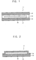
- FIG. 1 is a cross-sectional side view illustrating an embodiment of an organic light emitting display device according to the invention.
- an organic light emitting display device 11 may include a (base) substrate 20, an encapsulation substrate 30, and a display member 40.
- the substrate 20, the encapsulation substrate 30, and the display member 40 may together define a display panel of the organic light emitting display device.
- Such display panel may be disposed relative to other components of the organic light emitting display device, including but not limited to, a receiving container, cover, etc.
- the substrate 20 may include transparent material such as glass or plastic.
- the display member 40 may be disposed on the substrate 20.
- the display member 40 may generate and display an image with light.
- the display member 40 may be disposed on a center portion of a first surface 21 of the substrate 20.
- the display member 40 may be on the first surface 21 to be disposed spaced apart from ends or outer edges of the substrate 20.
- the display member 40 may display the image toward the substrate 20 and/or the encapsulation substrate 30.
- the encapsulation substrate 30 may be disposed on the display member 40.
- the encapsulation substrate 30 may face the first surface 21 of the substrate 20 with respect to the display member 40.
- the encapsulation substrate 30 may have substantially the same material as the substrate 20.
- the encapsulation substrate 30 may block impurities outside thereof, from penetrating into the display member 40.
- An (outer) edge portion of the substrate 20 and an (outer) edge portion of the encapsulation substrate 30 may be combined to each other by a sealing member 50.
- a space between the substrate 20 and the encapsulation substrate 30 may be encapsulated by the sealing member 50.
- a moisture absorbing member or a filling member may be disposed in the space.
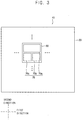
- FIG. 2 is a cross-sectional side view illustrating another embodiment of an organic light emitting display device according to the invention.
- an organic light emitting display device 11 may include a (base) substrate 20, an encapsulation thin film 35, and a display member 40.
- the encapsulation thin film 35 may be disposed on the display member 40 instead of the encapsulation substrate 30 (refer to FIG. 1 ).
- the encapsulation thin film 35 may protect the display member 40 from impurities similar to that described above for the encapsulation substrate 30.
- the encapsulation thin film 35 may have a structure in which at least one inorganic layer and at least one organic layer are alternately layered.
- the structure of the encapsulation thin film 35 is not limited thereto, and any transparent encapsulation structure may be applied which protects the display member 40 from impurities.
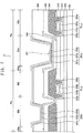
- FIG. 3 is a top plan view illustrating an embodiment of the display member of the organic light emitting display device in FIG. 1 .
- the display member illustrated in FIG. 3 may also be applied to the organic light emitting display device in FIG. 2 .
- the display member 40 may include a unit pixel 60 provided in plurality (indicated by the ⁇ disposed at each side of the unit pixel 60 in FIG. 3 ).
- the unit pixels 60 may be arranged along a first direction and a second direction, which cross each other.
- the first direction and the second direction may be substantially parallel to the substrate 20.
- the first direction and the second direction may define a plane which is parallel to the plane in which the substrate 20 and/or the first surface 21 thereof are disposed.
- the first direction and the second direction may be substantially orthogonal to each other in the top plan view, but the invention is not limited thereto.
- a thickness of the organic light emitting display device is taken in a third direction which crosses each of the first and second directions.
- the cross-sectional views of FIGS. 1 and 2 are defined in the third (thickness) direction, and another direction in the plane parallel to the plane in which the substrate 20 and/or the first surface 21 thereof are disposed, such as the first or second direction.
- Each unit pixel 60 may include a plurality of sub-pixels 70. Light generated at or transmitted through the sub-pixels 70 may be emitted from each of the sub-pixels 70.
- each unit pixel 60 may include a first sub-pixel 70a, a second sub-pixel 70b, and a third sub-pixel 70c.
- the number of the sub-pixels 70 within a single unit pixel 60 is not limited thereto, and each unit pixel 60 may include two, four or more sub-pixels 70.
- the first sub-pixel 70a, the second sub-pixel 70b, and the third sub-pixel 70c may emit blue light, green light and red light, respectively.
- Each unit pixel 60 may display a particular color by combining lights emitted from individual sub-pixels such as the first sub-pixel 70a, the second sub-pixel 70b, and the third sub-pixel 70c.
- FIG. 4 is an enlarged top plan view illustrating an embodiment of a unit pixel of the display member in FIG. 3 .
- each of the sub-pixels 70 may include an emission region and a non-emission region.
- the first sub-pixel 70a may include a first emission region 80a and a first non-emission region 90a.
- the second sub-pixel 70b may include a second emission region 80b and a second non-emission region 90b.
- the third sub-pixel 70c may include a third emission region 80c and a third non-emission region 90c.
- the sub-pixels 70 each including the emission region and the non-emission region may be spaced apart from each other (refer to FIG. 4 ) or may be directly adjacent to each other (refer to FIG. 5 , for example).
- Light may be emitted from the emission region.
- blue light may be emitted from the first emission region 80a
- green light may be emitted from the second emission region 80b
- red light may be emitted from the third emission region 80c.
- the non-emission region of a sub-pixel may be adjacent to the emission region thereof.
- the non-emission region may surround the emission region in the top plan view, that is, be disposed at all sides of the emission region.
- the first non-emission region 90a may surround the first emission region 80a
- the second non-emission region 90b may surround the second emission region 80b
- third non-emission region 90c may surround the third emission region 80c.
- a via insulation layer 140 may not overlap the emission region of at least one sub-pixel among the plurality of sub-pixels 70.
- the via insulation layer 140 may not overlap the first emission region 80a of the first sub-pixel 70a among the first sub-pixel 70a, the second sub-pixel 70b and the third sub-pixel 70c.
- the via insulation layer 140 may not overlap the second emission region 80b of the second sub-pixel 70b or the third emission region 80c of the third sub-pixel 70c, among the first sub-pixel 70a, the second sub-pixel 70b and the third sub-pixel 70c.
- FIG. 5 is an enlarged cross-sectional view illustrating an embodiment of an organic light emitting display device according to the invention.
- FIG. 5 may be an enlarged cross-sectional view illustrating an organic light emitting display device 11 according to the invention, taken along line I-I' in FIG. 4 .
- an organic light emitting display device 11 may include a substrate 20, transistors TR_a and TR_b, a via insulation layer 140, and organic light emitting elements 150a and 150b.
- the transistors TR_a and TR_b may be disposed on the substrate 20.
- the via insulation layer 140 may cover the transistors TR_a and TR_b.
- the organic light emitting elements 150a and 150b may be disposed on the substrate 20.
- the substrate 20 may include a collective emission region and a collective non-emission region, defined by these respective regions of the sub-pixels 70.
- FIG. 5 illustrates only the first sub-pixel 70a, which includes the first emission region 80a and the first non-emission region 90a, and the second sub-pixel 70b, which includes the second emission region 80b and the second non-emission region 90b.
- the third sub-pixel 70c which includes the third emission region 80c and the third non-emission region 90c, may be also disposed on the substrate 20.
- the third sub-pixel 70c may have substantially the same element or structure as the first sub-pixel 70a or the second sub-pixel 70b. Therefore, a description on the third sub-pixel 70c may be omitted.
- a buffer layer 105 may be disposed on the substrate 20, between the transistors and the substrate 20.
- the buffer layer 105 may have a flat surface facing the transistors, and may block a penetration of impurities from outside the organic light emitting display device 11.
- the buffer layer 105 may include an inorganic insulation material such as silicon oxide (SiOx), silicon nitride (SiNx), silicon oxynitride (SiOxNy), or the like. In an alternative embodiment, the buffer layer 105 may be omitted.
- a first transistor TR_a and a second transistor TR_b may be disposed on the substrate 20.
- the first transistor TR_a may supply a driving (electrical) current to a first organic light emitting element 150a
- the second transistor TR_b may supply a driving (electrical) current to a second organic light emitting element 150b.
- the first transistor TR_a may include a first active pattern 110a, a first gate electrode 120a, a first source electrode 130a and a first drain electrode 135a.
- the second transistor TR_b may include a second active pattern 110b, a second gate electrode 120b, a second source electrode 130b, and a second drain electrode 135b.
- the first transistor TR_a may be disposed in the first non-emission region 90a.
- the first active pattern 110a and the second active pattern 110b may be disposed on the buffer layer 105.
- the first active pattern 110a and the second active pattern 110b may include semiconductor material.
- the first active pattern 110a and the second active pattern 110b may include amorphous silicon, polycrystalline silicon, oxide semiconductor, or the like.
- Each of the first active pattern 110a and the second active pattern 110b may include or define a source region, a drain region, and a channel region disposed therebetween.
- a gate insulation layer 115 may be disposed on the buffer layer 105.
- the gate insulation layer 115 may cover the first active pattern 110a and the second active pattern 110b.
- the gate insulation layer 115 may include an inorganic insulation material such as silicon oxide (SiOx), silicon nitride (SiNx), silicon oxynitride (SiOxNy), or the like.
- the gate insulation layer 115 may insulate the first gate electrode 120a from the first active pattern 110a, and may insulate the second gate electrode 120b from the second active pattern 110b.
- the first gate electrode 120a and the second gate electrode 120b may be disposed on the gate insulation layer 115.
- the first gate electrode 120a may overlap the channel region of the first active pattern 110a.
- the second gate electrode 120b may overlap the channel region of the second active pattern 110b.
- the first gate electrode 120a and the second gate electrode 120b may include a metal material such as molybdenum (Mo), aluminum (Al), copper (Cu), titanium (Ti), or the like.
- An insulation interlayer 125 may be disposed on the gate insulation layer 115.
- the insulation interlayer 125 may cover the first gate electrode 120a and the second gate electrode 120b.
- the insulation interlayer 125 may include an inorganic insulation material such as silicon oxide (SiOx), silicon nitride (SiNx), silicon oxynitride (SiOxNy), or the like.
- the first source electrode 130a, the first drain electrode 135a, the second source electrode 130b and the second drain electrode 135b may be disposed on the insulation interlayer 125.
- the first source electrode 130a and the first drain electrode 135a may be in contact with the source region and the drain region of the first active pattern 110a, respectively, through contact holes in the insulation interlayer 125 and in the gate insulation layer 115.
- the second source electrode 130b and the second drain electrode 135b may be in contact with the source region and the drain region of the second active pattern 110b, respectively, through contact holes in the insulation interlayer 125 and in the gate insulation layer 115.
- the first source electrode 130a, the first drain electrode 135a, the second source electrode 130b, and the second drain electrode 135b may include a metal such as molybdenum (Mo), aluminum (Al), copper (Cu), titanium (Ti), or the like.
- the via insulation layer 140 may be disposed on the insulation interlayer 125.
- the via insulation layer 140 may be common to each of the sub-pixels 70 and to each of the unit pixels 60.
- the via insulation layer 140 may cover the first transistor TR_a and the second transistor TR_b.
- the via insulation layer 140 may cover the first source electrode 130a, the first drain electrode 135a, the second source electrode 130b, and the second drain electrode 135b.
- the via insulation layer 140 may have a flat top surface so as to alleviate an uneven surface derived from the first transistor TR_a and the second transistor TR_b, and so as to reduce or effectively prevent the occurrence of failure of structures within the organic light emitting display device 11 disposed on the via insulation layer 140.
- the via insulation layer 140 may include an organic insulation material such as polyimide (PI).
- PI polyimide
- the via insulation layer 140 may include or define an opening portion 141 and a contact hole.
- the opening portion 141 may be disposed or formed in the first emission region 80a, and may expose a portion of the insulation interlayer 125 and a portion of the first drain electrode 135a in the first emission region 80a.
- the contact hole may be disposed or formed on the second drain electrode 135b, and may expose a portion of the second drain electrode 135b.
- the via insulation layer 140 may be formed by using a photolithography process.
- a photosensitive organic insulation material layer may be formed on the insulation interlayer 125, and then the organic insulation material layer may be exposed and developed by using a mask so as to form the via insulation layer 140 including the opening portion 141 and the contact hole.
- a portion of the organic insulation material layer may be removed to form the opening portion 141, thus, a total volume of the via insulation layer 140 may decrease as compared to a via insulation layer which excludes the opening portion 141 at an emission region. Accordingly, since the total volume of the via insulation layer 140 including the opening portion 141 is decreased, the amount of outgas generated from the via insulation layer 140 may decrease.
- the first organic light emitting element 150a and the second organic light emitting element 150b may be disposed on the substrate 20.
- the first organic light emitting element 150a may be electrically connected to the first transistor TR_a
- the second organic light emitting element 150b may be electrically connected to the second transistor TR_b.
- the first organic light emitting element 150a may include a first pixel electrode 151a, a first organic light emitting layer 152a and a first common electrode 153a.
- the second organic light emitting element 150b may include a second pixel electrode 151b, a second organic light emitting layer 152b and a second common electrode 153b.
- the first organic light emitting element 150a may be disposed in the first emission region 80a, and the second organic light emitting element 150b may be disposed in the second emission region 80b.
- the first and second common electrodes 153a and 153b may be portions of a single common electrode disposed common to each of the sub-pixels 70 and the unit pixels 60, but the invention is not limited thereto.
- the via insulation layer 140 may not be disposed (e.g., is excluded) in the first emission region 80a. Therefore, the via insulation layer 140 may not be disposed under the first organic light emitting element 150a, and the first organic light emitting element 150a may be disposed directly on the insulation interlayer 125 including the inorganic insulation material. Because the first transistor TR_a is disposed in the first non-emission region 90a with the via insulation layer 140 disposed thereon, although the via insulation layer 140 is not disposed under the first organic light emitting element 150a in the first emission region 80a, damage to the first organic light emitting element 150a due to an uneven surface thereunder (such as what could be derived from the underlying first transistor TR_a in the first sub-pixel 70a) may not occur.
- Each of the first pixel electrode 151a and the second pixel electrode 151b may be patterned as an island shape discrete pattern shape.
- a center (e.g., non-edge) portion of the first pixel electrode 151a may be disposed on or at the insulation interlayer 125, and an edge portion of the first pixel electrode 151a may be disposed on or at a sidewall and a top surface of the via insulation layer 140.
- the first pixel electrode 151a may be in contact with the first drain electrode 135a through the opening portion 141 in the via insulation layer 140.
- the second pixel electrode 151b may be disposed on the via insulation layer 140, and may be in contact with the second drain electrode 135b through the contact hole in the via insulation layer 140.
- the first pixel electrode 151a and the second pixel electrode 151b may include a metal and/or transparent conductive material.
- a height of the via insulation layer 140 at a top surface thereof may be greater than a height of the first pixel electrode 151a at a bottom surface of the center portion thereof.
- Each of the height of the top surface of the via insulation layer 140 and the height of the bottom surface of the center portion of the first pixel electrode 151 a may be a height from a common reference, such as the substrate 20.
- the height at the top surface of the via insulation layer 140 may be a sum of a thickness of the buffer layer 105, a thickness of the gate insulation layer 115, a thickness of the insulation interlayer 125, and a thickness of the via insulation layer 140.
- the height at the bottom surface of the center portion of the first pixel electrode 151 a may be a sum of a thickness of the buffer layer 105, a thickness of the gate insulation layer 115, and a thickness of the insulation interlayer 125. Therefore, the height at the top surface of the via insulation layer 140 may be greater than the height at the bottom surface of the center portion of the first pixel electrode 151a, by the thickness of the via insulation layer 140.
- the thicknesses and heights described above, may be a maximum value of those dimensions, taken from the common reference.
- the height of the first pixel electrode 151a at the center portion thereof may be substantially the same as a height of the first drain electrode 135a of the first transistor TR_a.
- the center portion of the first pixel electrode 151a and the first drain electrode 135a may be disposed on or at a top surface of the insulation interlayer 125. Therefore, the height of the first pixel electrode 151a at the center portion thereof and the height of the first drain electrode 135a may be substantially the same.
- a pixel defining layer 160 may be disposed on the via insulation layer 140.
- the pixel defining layer 160 may cover an edge portion of the first pixel electrode 151 a and an edge portion of the second pixel electrode 151b.
- the pixel defining layer 160 may expose the center portion of the first pixel electrode 151a and the center portion of the second pixel electrode 151b so as to define the first emission region 80a and the second emission region 80b.
- the pixel defining layer 160 may include organic insulation material such as polyimide (PI).
- PI polyimide
- the pixel defining layer 160 may be disposed common to each of the sub-pixels 70 and the unit pixels 60, but the invention is not limited thereto.
- the first organic light emitting layer 152a and the second organic light emitting layer 152b may be disposed on the first pixel electrode 151a and the second pixel electrode 151b, respectively.
- the first organic light emitting layer 152a may emit blue light and the second organic light emitting layer 152b may emit green light.
- the first organic light emitting layer 152a may not overlap the via insulation layer 140.
- the via insulation layer 140 may not be disposed under the first organic light emitting layer 152a. That is, a maximum thickness of the via insulation layer 140 may not be disposed under the first organic light emitting layer 152a.
- an organic light emitting layer of an organic light emitting element may be damaged by an outgas generated from a via insulation layer when the via insulation layer is substantially disposed under the organic light emitting layer.
- the via insulation layer 140 may not be disposed under the first organic light emitting layer 152a.
- the first organic light emitting layer 152a thereof may not be influenced by such outgas. Accordingly, damage of the first organic light emitting layer 152a of the first sub-pixel 70a due to the outgas may be reduced or effectively prevented.
- the first common electrode 153a may face the first pixel electrode 151a with respect to the first organic light emitting layer 152a, and the second common electrode 153b may face the second pixel electrode 151b with respect to the second organic light emitting layer 152b.
- the first common electrode 153a and the second common electrode 153b may be integrally formed, that is, disposed common to each of the sub-pixels 70.
- the first common electrode 153a and the second common electrode 153b may include a metal and/or transparent conductive material.
- FIG. 6 is an enlarged cross-sectional view illustrating another embodiment of an organic light emitting display device according to the invention.
- FIG. 6 may be an enlarged cross-sectional view illustrating an embodiment of an organic light emitting display device 12 taken along line I-I' in FIG. 4 .
- an organic light emitting display device 12 may include a substrate 20, transistors TR_a and TR_b, a via insulation layer 240, a passivation layer 245, and organic light emitting elements 250a and 250b.
- the transistors TR_a and TR_b may be disposed on the substrate 20.
- a gate insulation layer 215 may be disposed on the buffer layer 205.
- the first transistor TR_a may include a first active pattern 210a, a first gate electrode 220a, a first source electrode 230a and a first drain electrode 235a.
- the second transistor TR_b may include a second active pattern 210b, a second gate electrode 220b, a second source electrode 230b, and a second drain electrode 235b.
- the first organic light emitting element 250a may include a first pixel electrode 251a, a first organic light emitting layer 252a and a first common electrode 253a.
- the second organic light emitting element 250b may include a second pixel electrode 251b, a second organic light emitting layer 252b and a second common electrode 253b.
- the via insulation layer 240 may cover the transistors TR_a and TR_b.
- the passivation layer 245 may cover the via insulation layer 240.
- the passivation layer 245 may be disposed common to each of the sub-pixels 70 and the unit pixels 60, but the invention is not limited thereto.
- the organic light emitting elements 250a and 250b may be disposed on the substrate 20. Detailed explanations on elements and/or structures of the organic light emitting display device 12 illustrated in FIG. 6 , which are substantially the same as or similar to those of the organic light emitting display device 11 illustrated in FIG. 5 may be omitted.
- the via insulation layer 240 may be disposed on the insulation interlayer 225.
- the via insulation layer 240 may include a first opening portion 241 and a first contact hole.
- the first opening portion 241 may be disposed or formed in the first emission region 80a, and may expose a portion of the insulation interlayer 225 and a portion of the first drain electrode 235a in the first emission region 80a.
- the first contact hole may be disposed or formed on the second drain electrode 235b, and may expose a portion of the second drain electrode 235b.
- the passivation layer 245 may be disposed on the via insulation layer 240.
- the passivation layer 245 may include an inorganic insulation material such as silicon oxide (SiOx), silicon nitride (SiNx), silicon oxynitride (SiOxNy), or the like.
- the passivation layer 245 may not overlap the first emission region 80a. In other words, the passivation layer 245 may not be disposed in the first emission region 80a.
- the passivation layer 245 may cover a top surface and a sidewall of the via insulation layer 240. Therefore, a permeation of outgas emitted from the via insulation layer 240 to other elements of the organic light emitting display device 12 may be blocked by the passivation layer 245, and the passivation layer 245 may serve as a blocking layer against the outgas.
- the passivation layer 245 may include or define a second opening portion 246 and a second contact hole.
- the second opening portion 246 may be disposed or formed in the first emission region 80a, and may expose a portion of the insulation interlayer 225 and a portion of the first drain electrode 235a in the first emission region 80a. In an embodiment, for example, the second opening portion 246 may be disposed or formed inside the first opening portion 241 of the via insulation layer 240.
- the second contact hole may be disposed or formed on the second drain electrode 235b, and may expose a portion of the second drain electrode 235b. In an embodiment, for example, the second contact hole may be disposed or formed inside the first contact hole.
- the via insulation layer 240 and the passivation layer 245 may be formed by using a photolithography process.
- a photosensitive organic insulation material layer may be formed on the insulation interlayer 225, and then the organic insulation material layer may be exposed and developed by using a first mask so as to form the via insulation layer 240 including the first opening portion 241 and the first contact hole.
- An inorganic insulation material layer and a photoresist layer may be sequentially formed on the via insulation layer 240, and then the photoresist layer may be exposed and developed by using a second mask and the inorganic insulation material layer may be etched so as to form the passivation layer 245 including the second opening portion 246 and the second contact hole.
- a portion of the organic insulation material layer may be removed to form the first opening portion 241 of the via insulation layer 240 and the inorganic insulation material layer may be formed thereon, thus, a total volume of the via insulation layer 240 may decrease as compared to a via insulation layer which excludes the opening portion 241 at an emission region. Accordingly, since the total volume of the via insulation layer 240 including the opening portion 241 is decreased, the amount of outgas generated from the via insulation layer 240 may decrease.
- Each of the first pixel electrode 251a and the second pixel electrode 251b may be patterned as an island shape.
- a center (e.g., non-edge) portion of the first pixel electrode 251a may be disposed on the insulation interlayer 225, and an edge portion of the first pixel electrode 251a may be disposed on or at a sidewall and a top surface of the passivation layer 245.
- the first pixel electrode 251a may be in contact with the first drain electrode 235a through the second opening portion 246.
- the second pixel electrode 251b may be disposed on the passivation layer 245, and may be in contact with the second drain electrode 235b through the second contact hole.
- the pixel defining layer 260 may be disposed on the passivation layer 245.
- the via insulation layer 240 may not be disposed in the first emission region 80a. Therefore, the via insulation layer 240 may not be disposed under the first organic light emitting element 250a, and the first organic light emitting element 250a may be disposed directly on the insulation interlayer 225 including the inorganic insulation material. Because the first transistor TR_a is disposed in the first non-emission region 90a, although the via insulation layer 240 is not disposed under the first organic light emitting element 250a in the first emission region 80a, damage to the first organic light emitting element 250a due to an uneven surface thereunder may not occur.
- FIG. 7 is an enlarged cross-sectional view illustrating still another embodiment of an organic light emitting display device according to the invention.
- FIG. 7 may be an enlarged cross-sectional view illustrating an embodiment of an organic light emitting display device 13 taken along line I-I' in FIG. 4 .
- an organic light emitting display device 13 may include a substrate 20, transistors TR_a and TR_b, a via insulation layer 340, a passivation layer 345, and organic light emitting elements 350a and 350b.
- a gate insulation layer 315 may be disposed on the buffer layer 305.
- the transistors TR_a and TR_b may be disposed on the substrate 20.
- the first transistor TR_a may include a first active pattern 310a, a first gate electrode 320a, a first source electrode 330a and a first drain electrode 335a.
- the second transistor TR_b may include a second active pattern 310b, a second gate electrode 320b, a second source electrode 330b, and a second drain electrode 335b.
- the first organic light emitting element 350a may include a first pixel electrode 351a, a first organic light emitting layer 352a and a first common electrode 353a.
- the second organic light emitting element 350b may include a second pixel electrode 351b, a second organic light emitting layer 352b and a second common electrode 353b.
- the via insulation layer 340 may cover the transistors TR_a and TR_b.
- the passivation layer 345 may cover the via insulation layer 340.
- the organic light emitting elements 350a and 350b may be disposed on the substrate 20. Detailed explanations on elements and/or structures of the organic light emitting display device 13 illustrated in FIG. 7 , which are substantially the same as or similar to those of the organic light emitting display device 12 illustrated in FIG. 6 may be omitted.
- the passivation layer 345 may be disposed on the via insulation layer 340.
- the passivation layer 345 may overlap the first emission region 80a in contrast with the passivation layer 245 illustrated in FIG. 6 .
- the passivation layer 345 may be disposed in the first emission region 80a as well as the first non-emission region 90a, the second emission region 80b and the second non-emission region 90b.
- the passivation layer 345 may have an entirely substantially uniform thickness according to a profile of the via insulation layer 340 and the insulation interlayer 325 disposed thereunder.
- the passivation layer 345 may include a third contact hole 346 and a second contact hole.
- the third contact hole 346 may be disposed or formed on the first drain electrode 335a, and may expose a portion of the first drain electrode 335a.
- the second contact hole may be formed on the second drain electrode 335b, and may expose a portion of the second drain electrode 335b.
- the via insulation layer 340 and the passivation layer 345 may be formed by using a photolithography process.
- a photosensitive organic insulation material layer may be formed on the insulation interlayer 325, and then the organic insulation material layer may be exposed and developed by using a first mask so as to form the via insulation layer 340 including the opening portion 341 and the first contact hole therein.
- An inorganic insulation material layer and a photoresist layer may be sequentially formed on the via insulation layer 340, and then the photoresist layer may be exposed and developed by using a second mask and the inorganic insulation material layer may be etched so as to form the passivation layer 345 including the third contact hole 346 and the second contact hole therein.
- a portion of the organic insulation material layer may be removed to form the opening portion 341 of the via insulation layer 340 and the inorganic insulation material layer may be formed thereon, thus, a total volume of the via insulation layer 340 may decrease as compared to a via insulation layer which excludes the opening portion 341 at an emission region. Accordingly, since the total volume of the via insulation layer 340 including the opening portion 341 is decreased, the amount of outgas generated from the via insulation layer 340 may decrease.
- Each of the first pixel electrode 351a and the second pixel electrode 351b may be patterned as an island shape.
- a center (e.g., non-edge) portion of the first pixel electrode 351a may be disposed on the passivation layer 345 positioned inside the opening portion 341, and an edge portion of the first pixel electrode 351a may be disposed on or at a sidewall and a top surface of the passivation layer 345.
- the first pixel electrode 351a may be in contact with the first drain electrode 335a through the third contact hole 346.
- the second pixel electrode 351b may be disposed on the passivation layer 345, and may be in contact with the second drain electrode 335b through the second contact hole.
- the pixel defining layer 360 may be disposed on the passivation layer 345.
- the via insulation layer 340 may not be disposed in the first emission region 80a. Therefore, the via insulation layer 340 may not be disposed under the first organic light emitting element 350a, and the first organic light emitting element 350a may be disposed directly on the passivation layer 345 including the inorganic insulation material. Because the first transistor TR_a is disposed in the first non-emission region 90a, although the via insulation layer 340 is not disposed under the first organic light emitting element 350a in the first emission region 80a, damage to the first organic light emitting element 350a due to an uneven surface thereunder may not occur.
- FIG. 8 is an enlarged cross-sectional view illustrating yet another embodiment of an organic light emitting display device according to the invention.
- FIG. 8 may be an enlarged cross-sectional view illustrating an embodiment of an organic light emitting display device 14 taken along line I-I' in FIG. 4 .
- an organic light emitting display device 14 may include a substrate 20, transistors TR_a and TR_b, a passivation layer 445, a via insulation layer 440, and organic light emitting elements 450a and 450b.
- a gate insulation layer 415 may be disposed on the buffer layer 405.
- the transistors TR_a and TR_b may be disposed on the substrate 20.
- the passivation layer 445 may cover the transistors TR_a and TR_b.
- the first transistor TR_a may include a first active pattern 410a, a first gate electrode 420a, a first source electrode 430a and a first drain electrode 435a.
- the second transistor TR_b may include a second active pattern 410b, a second gate electrode 420b, a second source electrode 430b, and a second drain electrode 435b.
- the first organic light emitting element 450a may include a first pixel electrode 451a, a first organic light emitting layer 452a and a first common electrode 453a.
- the second organic light emitting element 450b may include a second pixel electrode 451b, a second organic light emitting layer 452b and a second common electrode 453b.
- the via insulation layer 440 may be disposed on the passivation layer 445.
- the organic light emitting elements 450a and 450b may be disposed on the substrate 20.
- Detailed explanations on elements and/or structures of the organic light emitting display device 14 illustrated in FIG. 8 which are substantially the same as or similar to those of the organic light emitting display device 11 illustrated in FIG. 5 may be omitted.
- the passivation layer 445 may be disposed on the insulation interlayer 425.
- the passivation layer 445 may cover the first transistor TR_a and the second transistor TR_b.
- the passivation layer 445 may cover the first source electrode 430a, the first drain electrode 435a, the second source electrode 430b, and the second drain electrode 435b.
- the passivation layer 445 may include an inorganic insulation material such as silicon oxide (SiOx), silicon nitride (SiNx), silicon oxynitride (SiOxNy), or the like.
- the passivation layer 445 may not overlap the first emission region 80a. In other words, the passivation layer 445 may not be disposed in the first emission region 80a.
- the via insulation layer 440 may be disposed on the passivation layer 445.
- the passivation layer 445 and the via insulation layer 440 may include or collectively define an opening portion 441 and a contact hole.
- the opening portion 441 may be disposed or formed in the first emission region 80a, and may expose a portion of the insulation interlayer 425 and a portion of the first drain electrode 435a in the first emission region 80a.
- the contact hole may be disposed or formed on the second drain electrode 435b, and may expose a portion of the second drain electrode 435b.
- the passivation layer 445 and the via insulation layer 440 may be formed by using a photolithography process.
- an inorganic insulation material layer and a photoresist layer may be sequentially formed on the insulation interlayer 425, and then the photoresist layer may be exposed and developed by using a first mask and the inorganic insulation material layer may be etched so as to form the passivation layer 445 including a portion of the opening portion 441 and a portion of the contact hole.
- a photosensitive organic insulation material layer may be formed on the passivation layer 445, and then the organic insulation material layer may be exposed and developed by using a second mask so as to form the via insulation layer 440 including a remainder of the opening portion 441 and a remainder of the contact hole.
- an inorganic insulation material layer and a photosensitive organic insulation material layer may be sequentially formed on the insulation interlayer 425, and then the organic insulation material layer may be exposed and developed by using a mask and the inorganic insulation material layer may be etched so as to form the passivation layer 445 and the via insulation layer 440 which include a portion of the opening portion 441 and a portion of the contact hole.
- the via insulation layer 440 may serve as an etch-stop layer for the underlying inorganic insulation material layer.
- a portion of the organic insulation material layer may be removed to form the opening portion 441 and the inorganic insulation layer may be formed thereunder, thus, a total volume of the via insulation layer 440 may decrease as compared to a via insulation layer which excludes the opening portion 441 at an emission region. Accordingly, since the total volume of the via insulation layer 440 including the opening portion 441 is decreased, the amount of outgas generated from the via insulation layer 440 may decrease.
- Each of the first pixel electrode 451a and the second pixel electrode 451b may be patterned as an island shape.
- a center (e.g., non-edge) portion of the first pixel electrode 451a may be disposed on the insulation interlayer 425, and an edge portion of the first pixel electrode 451a may be disposed on or at a sidewall of the passivation layer 445, and a sidewall and a top surface of the via insulation layer 440.
- the first pixel electrode 451a may be in contact with the first drain electrode 435a through the opening portion 441.
- the second pixel electrode 451b may be disposed on the via insulation layer 440, and may be in contact with the second drain electrode 435b through the contact hole.
- the pixel defining layer 460 may be disposed on the via insulation layer 440.
- the via insulation layer 440 may not be disposed in the first emission region 80a. Therefore, the via insulation layer 440 may not be disposed under the first organic light emitting element 450a, and the first organic light emitting element 450a may be disposed directly on the insulation interlayer 425 including inorganic insulation material. Because the first transistor TR_a is disposed in the first non-emission region 90a, although the via insulation layer 440 is not disposed under the first organic light emitting element 450a in the first emission region 80a, damage on the first organic light emitting element 450a due to an uneven surface thereunder may not occur.
- FIG. 9 is an enlarged cross-sectional view illustrating yet another embodiment of an organic light emitting display device according to the invention.
- FIG. 9 may be an enlarged cross-sectional view illustrating an embodiment of an organic light emitting display device 15 taken along line I-I' in FIG. 4 .
- an organic light emitting display device 15 may include a substrate 20, transistors TR_a and TR_b, a passivation layer 545, a via insulation layer 540, and organic light emitting elements 550a and 550b.
- a gate insulation layer 515 may be disposed on the buffer layer 505.
- the transistors TR_a and TR_b may be disposed on the substrate 20.
- the passivation layer 545 may cover the transistors TR_a and TR_b.
- the first transistor TR_a may include a first active pattern 510a, a first gate electrode 520a, a first source electrode 530a and a first drain electrode 535a.
- the second transistor TR_b may include a second active pattern 510b, a second gate electrode 520b, a second source electrode 530b, and a second drain electrode 535b.
- the first organic light emitting element 550a may include a first pixel electrode 551a, a first organic light emitting layer 552a and a first common electrode 553a.
- the second organic light emitting element 550b may include a second pixel electrode 551b, a second organic light emitting layer 552b and a second common electrode 553b.
- the via insulation layer 540 may be disposed on the passivation layer 545.
- the organic light emitting elements 550a and 550b may be disposed on the substrate 20.
- Detailed explanations on elements and/or structures of the organic light emitting display device 15 illustrated in FIG. 9 which are substantially the same as or similar to those of the organic light emitting display device 14 illustrated in FIG. 8 may be omitted.
- the passivation layer 545 may be disposed on the insulation interlayer 525.
- the passivation layer 545 may overlap the first emission region 80a in contrast with the passivation layer 445 illustrated in FIG. 8 .
- the passivation layer 545 may be disposed in the first emission region 80a as well as the first non-emission region 90a, the second emission region 80b and the second non-emission region 90b.
- the passivation layer 545 may include a first contact hole 546 and a portion of a second contact hole.
- the first contact hole 546 may be disposed or formed on the first drain electrode 535a, and may expose a portion of the first drain electrode 535a.
- the portion of the second contact hole may be disposed or formed on the second drain electrode 535b, and may expose a portion of the second drain electrode 535b.
- the via insulation layer 540 may be disposed on the passivation layer 545.
- the via insulation layer 540 may include an opening portion 541 and a remainder of the second contact hole.
- the opening portion 541 may be disposed or formed in the first emission region 80a, and may expose a portion of the passivation layer 545 and a portion of the first drain electrode 535a in the first emission region 80a.
- the remainder of the second contact hole may be disposed or formed on the second drain electrode 535b, and may expose a portion of the second drain electrode 535b.
- the passivation layer 545 and the via insulation layer 540 may be formed by using a photolithography process.
- an inorganic insulation material layer and a photoresist layer may be sequentially formed on the insulation interlayer 525, and then the photoresist layer may be exposed and developed by using a first mask and the inorganic insulation material layer may be etched so as to form the passivation layer 545 including the first contact hole 546 and a portion of the second contact hole.
- a photosensitive organic insulation material layer may be formed on the passivation layer 545, and then the organic insulation material layer may be exposed and developed by using a second mask so as to form the via insulation layer 540 including the opening portion 541 and the remainder of the second contact hole.
- a portion of the organic insulation material layer may be removed to form the opening portion 541 and the inorganic insulation material layer may be formed thereunder, thus, a total volume of the via insulation layer 540 may decrease as compared to a via insulation layer which excludes the opening portion 541 at an emission region. Accordingly, since the total volume of the via insulation layer 540 including the opening portion 541 is decreased, the amount of outgas generated from the via insulation layer 540 may decrease.
- Each of the first pixel electrode 551a and the second pixel electrode 551b may be patterned as an island shape.
- a center portion of the first pixel electrode 551a may be disposed on the passivation layer 545, and an edge portion of the first pixel electrode 551a may be disposed on or at a sidewall and a top surface of the via insulation layer 540.
- the first pixel electrode 551a may be in contact with the first drain electrode 535a through the first contact hole 546.
- the second pixel electrode 551b may be disposed on the via insulation layer 540, and may be in contact with the second drain electrode 535b through the second contact hole.
- the pixel defining layer 560 may be disposed on the via insulation layer 540.
- the via insulation layer 540 may not be disposed in the first emission region 80a. Therefore, the via insulation layer 540 may not be disposed under the first organic light emitting element 550a, and the first organic light emitting element 550a may be disposed directly on the passivation layer 545 including inorganic insulation material. Because the first transistor TR_a is disposed in the first non-emission region 90a, although the via insulation layer 540 is not disposed under the first organic light emitting element 550a in the first emission region 80a, damage on the first organic light emitting element 550a due to an uneven surface thereunder may not occur.
- the organic light emitting display device may be applied to a display device included in a computer, a notebook, a mobile phone, a smartphone, a smart pad, a portable media player ("PMP"), a personal digital assistant (“PDA”), an MP3 player, or the like.
- PMP portable media player
- PDA personal digital assistant
Landscapes
- Engineering & Computer Science (AREA)
- Microelectronics & Electronic Packaging (AREA)
- Electroluminescent Light Sources (AREA)
- Devices For Indicating Variable Information By Combining Individual Elements (AREA)
- Physics & Mathematics (AREA)
- Optics & Photonics (AREA)
Abstract
Description
- Embodiments relate to display devices. More particularly, embodiments relate to organic light emitting display devices.
- An organic light emitting display device may have an organic light emitting element including a hole injection layer, an electron injection layer, and an organic light emitting layer formed therebetween. In the organic light emitting display device, light may be generated as excitons, which are the combination of holes injected from the hole injection layer and electrons injected from the electron injection layer, fall from an excited state to a ground state.
- The organic light emitting display device may not include a separate light source to generate light, and thus the organic light emitting display device may have relatively small thickness and light weight as well as relatively low power consumption. Furthermore, the organic light emitting display device may have relatively wide viewing angle, high contrast and high response speed, etc.
- One or more embodiment provides an organic light emitting display device for preventing damage of an organic light emitting layer.
- One or more embodiment provides an organic light emitting display device for reducing or effectively preventing damage of an organic light emitting element.
- An organic light emitting display device according to one or more embodiment includes a substrate including an emission region and a non-emission region, an organic light emitting element which emits light, the organic light emitting element including a first electrode disposed on the substrate in the emission region, an organic light emitting layer disposed on the first electrode in the emission region, and a second electrode disposed on the organic light emitting layer, and a via insulation layer disposed on the substrate in the non-emission region thereof, the via insulation layer including an organic insulation material. The via insulation layer defines an opening therein in which the organic light emitting layer of the organic light emitting element is disposed.
- In an embodiment, a maximum height of a top surface of the via insulation layer from the substrate may be greater than a height of a bottom surface of a center portion of the first electrode from the substrate.
- In an embodiment, the organic light emitting display device may further include a transistor connected to the organic light emitting element in the emission region of the substrate, the transistor disposed on the substrate in the non-emission region.
- In an embodiment, from the substrate, the height of the bottom surface of the center portion of the first electrode may be disposed at same height as a drain electrode of the transistor.
- In an embodiment, the organic light emitting display device may further include a passivation layer including an inorganic insulation material, the passivation layer disposing the via insulation layer between the passivation layer and the substrate.
- In an embodiment, the passivation layer may extend along a top surface and a sidewall of the via insulation layer.
- In an embodiment, the passivation layer may be disposed only in the non-emission region.
- In an embodiment, the passivation layer may be disposed in the non-emission region and in the emission region.
- In an embodiment, the organic light emitting display device may further include a passivation layer disposed between the substrate and the via insulation layer, the passivation layer including an inorganic insulation material.
- In an embodiment, the passivation layer may be disposed only in the non-emission region.
- In an embodiment, the passivation layer may be disposed in the non-emission region and in the emission region.
- An organic light emitting display device according to one or more embodiment includes a substrate, a plurality of sub-pixels disposed on the substrate, the plurality of sub-pixels each including an organic light emitting element, and a via insulation layer disposed on the substrate in each of the sub-pixels including the organic light emitting element, the via insulation layer including an organic insulation material. The via insulation layer defines an opening therein in which the organic light emitting element of at least one sub-pixel among the plurality of sub-pixels is disposed.
- In an embodiment, the plurality of sub-pixels may include a blue sub-pixel, a green sub-pixel, and a red sub-pixel. The organic light emitting element of the blue sub-pixel may be disposed in the opening of the via insulation layer.
- In an embodiment, the organic light emitting display device may further include a passivation layer disposed between the via insulation layer and the organic light emitting element, the passivation layer including an inorganic insulation material.
- In an embodiment, the passivation layer may extend along a top surface and a sidewall of the via insulation layer.
- In an embodiment, the passivation layer may define an opening in which the organic light emitting element of the at least one sub-pixel is disposed.
- In an embodiment, the passivation layer may be disposed between the organic light emitting element of the at least one sub-pixel and the substrate.
- In an embodiment, the organic light emitting display device may further include a passivation layer disposed between the substrate and the via insulation layer, the passivation layer including an inorganic insulation material.
- In an embodiment, the passivation layer may define an opening in which the organic light emitting element of the at least one sub-pixel is disposed.
- In an embodiment, the passivation layer may be disposed between the organic light emitting element of the at least one sub-pixel and the substrate.
- The organic light emitting display device according to one or more embodiment may include the via insulation layer which may not overlap the organic light emitting layer, therefore, damage to the organic light emitting layer may be reduced or effectively prevented. The organic light emitting display device according to one or more embodiment may include the via insulation layer which may not overlap the organic light emitting element of at least one sub-pixel, therefore, damage to the organic light emitting element may be reduced or effectively prevented.
- Illustrative, non-limiting embodiments will be more clearly understood from the following detailed description taken in conjunction with the accompanying drawings.
-
FIG. 1 is a cross-sectional side view illustrating an embodiment of an organic light emitting display device according to the invention. -
FIG. 2 is a cross-sectional side view illustrating another embodiment of an organic light emitting display device according to the invention. -
FIG. 3 is a top plan view illustrating an embodiment of a display member of the organic light emitting display device inFIG. 1 . -
FIG. 4 is an enlarged top plan view illustrating an embodiment of a unit pixel of the display member inFIG. 3 . -
FIG. 5 is an enlarged cross-sectional view illustrating an embodiment of an organic light emitting display device according to the invention. -
FIG. 6 is an enlarged cross-sectional view illustrating another embodiment of an organic light emitting display device according to the invention. -
FIG. 7 is an enlarged cross-sectional view illustrating still another embodiment of an organic light emitting display device according to the invention. -
FIG. 8 is an enlarged cross-sectional view illustrating yet another embodiment of an organic light emitting display device according to the invention. -
FIG. 9 is an enlarged cross-sectional view illustrating yet another embodiment of an organic light emitting display device according to the invention. - The invention now will be described more fully hereinafter with reference to the accompanying drawings, in which various embodiments are shown. This invention may, however, be embodied in many different forms, and should not be construed as limited to the embodiments set forth herein. Rather, these embodiments are provided so that this disclosure will be thorough and complete, and will fully convey the scope of the invention to those skilled in the art. Like reference numerals refer to like elements throughout.
- It will be understood that when an element is referred to as being "on" another element, it can be directly on the other element or intervening elements may be present therebetween. In contrast, when an element is referred to as being "directly on" another element, there are no intervening elements present.
- It will be understood that, although the terms "first," "second," "third" etc. may be used herein to describe various elements, components, regions, layers and/or sections, these elements, components, regions, layers and/or sections should not be limited by these terms. These terms are only used to distinguish one element, component, region, layer or section from another element, component, region, layer or section. Thus, "a first element," "component," "region," "layer" or "section" discussed below could be termed a second element, component, region, layer or section without departing from the teachings herein.
- The terminology used herein is for the purpose of describing particular embodiments only and is not intended to be limiting. As used herein, the singular forms "a," "an," and "the" are intended to include the plural forms, including "at least one," unless the content clearly indicates otherwise. "At least one" is not to be construed as limiting "a" or "an." "Or" means "and/or." As used herein, the term "and/or" includes any and all combinations of one or more of the associated listed items. It will be further understood that the terms "comprises" and/or "comprising," or "includes" and/or "including" when used in this specification, specify the presence of stated features, regions, integers, steps, operations, elements, and/or components, but do not preclude the presence or addition of one or more other features, regions, integers, steps, operations, elements, components, and/or groups thereof.
- Furthermore, relative terms, such as "lower" or "bottom" and "upper" or "top," may be used herein to describe one element's relationship to another element as illustrated in the Figures. It will be understood that relative terms are intended to encompass different orientations of the device in addition to the orientation depicted in the Figures. For example, if the device in one of the figures is turned over, elements described as being on the "lower" side of other elements would then be oriented on "upper" sides of the other elements. The exemplary term "lower," can therefore, encompasses both an orientation of "lower" and "upper," depending on the particular orientation of the figure. Similarly, if the device in one of the figures is turned over, elements described as "below" or "beneath" other elements would then be oriented "above" the other elements. The exemplary terms "below" or "beneath" can, therefore, encompass both an orientation of above and below.
- Unless otherwise defined, all terms (including technical and scientific terms) used herein have the same meaning as commonly understood by one of ordinary skill in the art to which this disclosure belongs. It will be further understood that terms, such as those defined in commonly used dictionaries, should be interpreted as having a meaning that is consistent with their meaning in the context of the relevant art and the present disclosure, and will not be interpreted in an idealized or overly formal sense unless expressly so defined herein.
- Exemplary embodiments are described herein with reference to cross section illustrations that are schematic illustrations of idealized embodiments. As such, variations from the shapes of the illustrations as a result, for example, of manufacturing techniques and/or tolerances, are to be expected. Thus, embodiments described herein should not be construed as limited to the particular shapes of regions as illustrated herein but are to include deviations in shapes that result, for example, from manufacturing. For example, a region illustrated or described as flat may, typically, have rough and/or nonlinear features. Moreover, sharp angles that are illustrated may be rounded. Thus, the regions illustrated in the figures are schematic in nature and their shapes are not intended to illustrate the precise shape of a region and are not intended to limit the scope of the present claims.
- Hereinafter, organic light emitting display devices in accordance with embodiments of the present disclosure will be explained in detail with reference to the accompanying drawings.
- An organic light emitting display device may include a display panel which generates an image with light. The display panel may include an organic light emitting element which generates the light for displaying the image, a transistor which drives the organic light emitting element to generate the light for displaying the image, and a via insulation layer. The via insulation layer may protect the transistor which drives the organic light emitting element and may planarize a top surface of the transistor within the display panel. The via insulation layer may include organic material.
- The via insulation layer including the organic material may generate an outgas due to relatively short-term or long-term chemical dissolution thereof. The outgas may be undesirably injected into an organic light emitting layer of the organic light emitting element, so that damages such as a dark spot, a pixel shrinkage, etc. may undesirably occur.
-
FIG. 1 is a cross-sectional side view illustrating an embodiment of an organic light emitting display device according to the invention. - Referring to
FIG. 1 , an organic light emittingdisplay device 11 according to an embodiment may include a (base)substrate 20, anencapsulation substrate 30, and adisplay member 40. Thesubstrate 20, theencapsulation substrate 30, and thedisplay member 40 may together define a display panel of the organic light emitting display device. Such display panel may be disposed relative to other components of the organic light emitting display device, including but not limited to, a receiving container, cover, etc. - The
substrate 20 may include transparent material such as glass or plastic. Thedisplay member 40 may be disposed on thesubstrate 20. Thedisplay member 40 may generate and display an image with light. In an embodiment, for example, thedisplay member 40 may be disposed on a center portion of afirst surface 21 of thesubstrate 20. Thedisplay member 40 may be on thefirst surface 21 to be disposed spaced apart from ends or outer edges of thesubstrate 20. Thedisplay member 40 may display the image toward thesubstrate 20 and/or theencapsulation substrate 30. - The
encapsulation substrate 30 may be disposed on thedisplay member 40. Theencapsulation substrate 30 may face thefirst surface 21 of thesubstrate 20 with respect to thedisplay member 40. Theencapsulation substrate 30 may have substantially the same material as thesubstrate 20. Theencapsulation substrate 30 may block impurities outside thereof, from penetrating into thedisplay member 40. - An (outer) edge portion of the
substrate 20 and an (outer) edge portion of theencapsulation substrate 30 may be combined to each other by a sealingmember 50. A space between thesubstrate 20 and theencapsulation substrate 30 may be encapsulated by the sealingmember 50. A moisture absorbing member or a filling member may be disposed in the space. -
FIG. 2 is a cross-sectional side view illustrating another embodiment of an organic light emitting display device according to the invention. - Referring to
FIG. 2 , an organic light emittingdisplay device 11 according to another embodiment may include a (base)substrate 20, an encapsulationthin film 35, and adisplay member 40. - As illustrated in
FIG. 2 , the encapsulationthin film 35 may be disposed on thedisplay member 40 instead of the encapsulation substrate 30 (refer toFIG. 1 ). The encapsulationthin film 35 may protect thedisplay member 40 from impurities similar to that described above for theencapsulation substrate 30. The encapsulationthin film 35 may have a structure in which at least one inorganic layer and at least one organic layer are alternately layered. However, the structure of the encapsulationthin film 35 is not limited thereto, and any transparent encapsulation structure may be applied which protects thedisplay member 40 from impurities. -
FIG. 3 is a top plan view illustrating an embodiment of the display member of the organic light emitting display device inFIG. 1 . The display member illustrated inFIG. 3 may also be applied to the organic light emitting display device inFIG. 2 . - Referring to
FIG. 3 , thedisplay member 40 may include aunit pixel 60 provided in plurality (indicated by the ●●● disposed at each side of theunit pixel 60 inFIG. 3 ). Theunit pixels 60 may be arranged along a first direction and a second direction, which cross each other. The first direction and the second direction may be substantially parallel to thesubstrate 20. The first direction and the second direction may define a plane which is parallel to the plane in which thesubstrate 20 and/or thefirst surface 21 thereof are disposed. The first direction and the second direction may be substantially orthogonal to each other in the top plan view, but the invention is not limited thereto. A thickness of the organic light emitting display device is taken in a third direction which crosses each of the first and second directions. The cross-sectional views ofFIGS. 1 and 2 are defined in the third (thickness) direction, and another direction in the plane parallel to the plane in which thesubstrate 20 and/or thefirst surface 21 thereof are disposed, such as the first or second direction. - Each
unit pixel 60 may include a plurality ofsub-pixels 70. Light generated at or transmitted through the sub-pixels 70 may be emitted from each of the sub-pixels 70. In an embodiment, eachunit pixel 60 may include afirst sub-pixel 70a, asecond sub-pixel 70b, and athird sub-pixel 70c. However, the number of the sub-pixels 70 within asingle unit pixel 60 is not limited thereto, and eachunit pixel 60 may include two, four or more sub-pixels 70. - In an embodiment, the
first sub-pixel 70a, thesecond sub-pixel 70b, and thethird sub-pixel 70c may emit blue light, green light and red light, respectively. Eachunit pixel 60 may display a particular color by combining lights emitted from individual sub-pixels such as thefirst sub-pixel 70a, thesecond sub-pixel 70b, and thethird sub-pixel 70c. -
FIG. 4 is an enlarged top plan view illustrating an embodiment of a unit pixel of the display member inFIG. 3 . - Referring to
FIG. 4 , each of the sub-pixels 70 may include an emission region and a non-emission region. Thefirst sub-pixel 70a may include afirst emission region 80a and a firstnon-emission region 90a. Thesecond sub-pixel 70b may include asecond emission region 80b and a secondnon-emission region 90b. Thethird sub-pixel 70c may include athird emission region 80c and a thirdnon-emission region 90c. The sub-pixels 70 each including the emission region and the non-emission region may be spaced apart from each other (refer toFIG. 4 ) or may be directly adjacent to each other (refer toFIG. 5 , for example). - Light may be emitted from the emission region. In an embodiment, for example, blue light may be emitted from the
first emission region 80a, green light may be emitted from thesecond emission region 80b, and red light may be emitted from thethird emission region 80c. - The non-emission region of a sub-pixel may be adjacent to the emission region thereof. In an embodiment, for example, the non-emission region may surround the emission region in the top plan view, that is, be disposed at all sides of the emission region. Referring to
FIG. 4 , for example, the firstnon-emission region 90a may surround thefirst emission region 80a, the secondnon-emission region 90b may surround thesecond emission region 80b, and thirdnon-emission region 90c may surround thethird emission region 80c. - A via
insulation layer 140 may not overlap the emission region of at least one sub-pixel among the plurality ofsub-pixels 70. In an embodiment, the viainsulation layer 140 may not overlap thefirst emission region 80a of thefirst sub-pixel 70a among thefirst sub-pixel 70a, thesecond sub-pixel 70b and thethird sub-pixel 70c. However, in another embodiment, the viainsulation layer 140 may not overlap thesecond emission region 80b of thesecond sub-pixel 70b or thethird emission region 80c of thethird sub-pixel 70c, among thefirst sub-pixel 70a, thesecond sub-pixel 70b and thethird sub-pixel 70c. A detail of the viainsulation layer 140 will be explained below with reference toFIG. 5 . -
FIG. 5 is an enlarged cross-sectional view illustrating an embodiment of an organic light emitting display device according to the invention. For example,FIG. 5 may be an enlarged cross-sectional view illustrating an organic light emittingdisplay device 11 according to the invention, taken along line I-I' inFIG. 4 . - Referring to
FIG. 5 , an organic light emittingdisplay device 11 according to an embodiment may include asubstrate 20, transistors TR_a and TR_b, a viainsulation layer 140, and organiclight emitting elements substrate 20. The viainsulation layer 140 may cover the transistors TR_a and TR_b. The organiclight emitting elements substrate 20. - The
substrate 20 may include a collective emission region and a collective non-emission region, defined by these respective regions of the sub-pixels 70.FIG. 5 illustrates only thefirst sub-pixel 70a, which includes thefirst emission region 80a and the firstnon-emission region 90a, and thesecond sub-pixel 70b, which includes thesecond emission region 80b and the secondnon-emission region 90b. However, thethird sub-pixel 70c, which includes thethird emission region 80c and the thirdnon-emission region 90c, may be also disposed on thesubstrate 20. Thethird sub-pixel 70c may have substantially the same element or structure as thefirst sub-pixel 70a or thesecond sub-pixel 70b. Therefore, a description on thethird sub-pixel 70c may be omitted. - A
buffer layer 105 may be disposed on thesubstrate 20, between the transistors and thesubstrate 20. Thebuffer layer 105 may have a flat surface facing the transistors, and may block a penetration of impurities from outside the organic light emittingdisplay device 11. Thebuffer layer 105 may include an inorganic insulation material such as silicon oxide (SiOx), silicon nitride (SiNx), silicon oxynitride (SiOxNy), or the like. In an alternative embodiment, thebuffer layer 105 may be omitted. - A first transistor TR_a and a second transistor TR_b may be disposed on the
substrate 20. The first transistor TR_a may supply a driving (electrical) current to a first organiclight emitting element 150a, and the second transistor TR_b may supply a driving (electrical) current to a second organiclight emitting element 150b. The first transistor TR_a may include a firstactive pattern 110a, afirst gate electrode 120a, afirst source electrode 130a and afirst drain electrode 135a. The second transistor TR_b may include a secondactive pattern 110b, asecond gate electrode 120b, asecond source electrode 130b, and asecond drain electrode 135b. In an embodiment, the first transistor TR_a may be disposed in the firstnon-emission region 90a. - The first
active pattern 110a and the secondactive pattern 110b may be disposed on thebuffer layer 105. The firstactive pattern 110a and the secondactive pattern 110b may include semiconductor material. In an embodiment, for example, the firstactive pattern 110a and the secondactive pattern 110b may include amorphous silicon, polycrystalline silicon, oxide semiconductor, or the like. Each of the firstactive pattern 110a and the secondactive pattern 110b may include or define a source region, a drain region, and a channel region disposed therebetween. - A
gate insulation layer 115 may be disposed on thebuffer layer 105. Thegate insulation layer 115 may cover the firstactive pattern 110a and the secondactive pattern 110b. Thegate insulation layer 115 may include an inorganic insulation material such as silicon oxide (SiOx), silicon nitride (SiNx), silicon oxynitride (SiOxNy), or the like. Thegate insulation layer 115 may insulate thefirst gate electrode 120a from the firstactive pattern 110a, and may insulate thesecond gate electrode 120b from the secondactive pattern 110b. - The
first gate electrode 120a and thesecond gate electrode 120b may be disposed on thegate insulation layer 115. Thefirst gate electrode 120a may overlap the channel region of the firstactive pattern 110a. Thesecond gate electrode 120b may overlap the channel region of the secondactive pattern 110b. Thefirst gate electrode 120a and thesecond gate electrode 120b may include a metal material such as molybdenum (Mo), aluminum (Al), copper (Cu), titanium (Ti), or the like. - An
insulation interlayer 125 may be disposed on thegate insulation layer 115. Theinsulation interlayer 125 may cover thefirst gate electrode 120a and thesecond gate electrode 120b. Theinsulation interlayer 125 may include an inorganic insulation material such as silicon oxide (SiOx), silicon nitride (SiNx), silicon oxynitride (SiOxNy), or the like. - The
first source electrode 130a, thefirst drain electrode 135a, thesecond source electrode 130b and thesecond drain electrode 135b may be disposed on theinsulation interlayer 125. Thefirst source electrode 130a and thefirst drain electrode 135a may be in contact with the source region and the drain region of the firstactive pattern 110a, respectively, through contact holes in theinsulation interlayer 125 and in thegate insulation layer 115. Thesecond source electrode 130b and thesecond drain electrode 135b may be in contact with the source region and the drain region of the secondactive pattern 110b, respectively, through contact holes in theinsulation interlayer 125 and in thegate insulation layer 115. Thefirst source electrode 130a, thefirst drain electrode 135a, thesecond source electrode 130b, and thesecond drain electrode 135b may include a metal such as molybdenum (Mo), aluminum (Al), copper (Cu), titanium (Ti), or the like. - The via
insulation layer 140 may be disposed on theinsulation interlayer 125. The viainsulation layer 140 may be common to each of the sub-pixels 70 and to each of theunit pixels 60. The viainsulation layer 140 may cover the first transistor TR_a and the second transistor TR_b. In an embodiment, for example, the viainsulation layer 140 may cover thefirst source electrode 130a, thefirst drain electrode 135a, thesecond source electrode 130b, and thesecond drain electrode 135b. The viainsulation layer 140 may have a flat top surface so as to alleviate an uneven surface derived from the first transistor TR_a and the second transistor TR_b, and so as to reduce or effectively prevent the occurrence of failure of structures within the organic light emittingdisplay device 11 disposed on the viainsulation layer 140. The viainsulation layer 140 may include an organic insulation material such as polyimide (PI). The viainsulation layer 140 may not overlap thefirst emission region 80a, among the emission regions in aunit pixel 60. In other words, the viainsulation layer 140 may not be disposed in thefirst emission region 80a. - The via
insulation layer 140 may include or define anopening portion 141 and a contact hole. Theopening portion 141 may be disposed or formed in thefirst emission region 80a, and may expose a portion of theinsulation interlayer 125 and a portion of thefirst drain electrode 135a in thefirst emission region 80a. The contact hole may be disposed or formed on thesecond drain electrode 135b, and may expose a portion of thesecond drain electrode 135b. - In an embodiment of manufacturing the organic light emitting
display device 11, the viainsulation layer 140 may be formed by using a photolithography process. In an embodiment, a photosensitive organic insulation material layer may be formed on theinsulation interlayer 125, and then the organic insulation material layer may be exposed and developed by using a mask so as to form the viainsulation layer 140 including theopening portion 141 and the contact hole. A portion of the organic insulation material layer may be removed to form theopening portion 141, thus, a total volume of the viainsulation layer 140 may decrease as compared to a via insulation layer which excludes theopening portion 141 at an emission region. Accordingly, since the total volume of the viainsulation layer 140 including theopening portion 141 is decreased, the amount of outgas generated from the viainsulation layer 140 may decrease. - The first organic
light emitting element 150a and the second organiclight emitting element 150b may be disposed on thesubstrate 20. The first organiclight emitting element 150a may be electrically connected to the first transistor TR_a, and the second organiclight emitting element 150b may be electrically connected to the second transistor TR_b. The first organiclight emitting element 150a may include afirst pixel electrode 151a, a first organiclight emitting layer 152a and a firstcommon electrode 153a. The second organiclight emitting element 150b may include asecond pixel electrode 151b, a second organiclight emitting layer 152b and a secondcommon electrode 153b. The first organiclight emitting element 150a may be disposed in thefirst emission region 80a, and the second organiclight emitting element 150b may be disposed in thesecond emission region 80b. The first and secondcommon electrodes unit pixels 60, but the invention is not limited thereto. - As described above, the via
insulation layer 140 may not be disposed (e.g., is excluded) in thefirst emission region 80a. Therefore, the viainsulation layer 140 may not be disposed under the first organiclight emitting element 150a, and the first organiclight emitting element 150a may be disposed directly on theinsulation interlayer 125 including the inorganic insulation material. Because the first transistor TR_a is disposed in the firstnon-emission region 90a with the viainsulation layer 140 disposed thereon, although the viainsulation layer 140 is not disposed under the first organiclight emitting element 150a in thefirst emission region 80a, damage to the first organiclight emitting element 150a due to an uneven surface thereunder (such as what could be derived from the underlying first transistor TR_a in thefirst sub-pixel 70a) may not occur. - Each of the
first pixel electrode 151a and thesecond pixel electrode 151b may be patterned as an island shape discrete pattern shape. At theopening portion 141, a center (e.g., non-edge) portion of thefirst pixel electrode 151a may be disposed on or at theinsulation interlayer 125, and an edge portion of thefirst pixel electrode 151a may be disposed on or at a sidewall and a top surface of the viainsulation layer 140. Thefirst pixel electrode 151a may be in contact with thefirst drain electrode 135a through theopening portion 141 in the viainsulation layer 140. Thesecond pixel electrode 151b may be disposed on the viainsulation layer 140, and may be in contact with thesecond drain electrode 135b through the contact hole in the viainsulation layer 140. Thefirst pixel electrode 151a and thesecond pixel electrode 151b may include a metal and/or transparent conductive material. - In an embodiment, a height of the via
insulation layer 140 at a top surface thereof may be greater than a height of thefirst pixel electrode 151a at a bottom surface of the center portion thereof. Each of the height of the top surface of the viainsulation layer 140 and the height of the bottom surface of the center portion of thefirst pixel electrode 151 a may be a height from a common reference, such as thesubstrate 20. In an embodiment, for example, the height at the top surface of the viainsulation layer 140 may be a sum of a thickness of thebuffer layer 105, a thickness of thegate insulation layer 115, a thickness of theinsulation interlayer 125, and a thickness of the viainsulation layer 140. The height at the bottom surface of the center portion of thefirst pixel electrode 151 a may be a sum of a thickness of thebuffer layer 105, a thickness of thegate insulation layer 115, and a thickness of theinsulation interlayer 125. Therefore, the height at the top surface of the viainsulation layer 140 may be greater than the height at the bottom surface of the center portion of thefirst pixel electrode 151a, by the thickness of the viainsulation layer 140. The thicknesses and heights described above, may be a maximum value of those dimensions, taken from the common reference. - In an embodiment, the height of the
first pixel electrode 151a at the center portion thereof may be substantially the same as a height of thefirst drain electrode 135a of the first transistor TR_a. In an embodiment, for example, the center portion of thefirst pixel electrode 151a and thefirst drain electrode 135a may be disposed on or at a top surface of theinsulation interlayer 125. Therefore, the height of thefirst pixel electrode 151a at the center portion thereof and the height of thefirst drain electrode 135a may be substantially the same. - A
pixel defining layer 160 may be disposed on the viainsulation layer 140. Thepixel defining layer 160 may cover an edge portion of thefirst pixel electrode 151 a and an edge portion of thesecond pixel electrode 151b. Thepixel defining layer 160 may expose the center portion of thefirst pixel electrode 151a and the center portion of thesecond pixel electrode 151b so as to define thefirst emission region 80a and thesecond emission region 80b. Thepixel defining layer 160 may include organic insulation material such as polyimide (PI). Thepixel defining layer 160 may be disposed common to each of the sub-pixels 70 and theunit pixels 60, but the invention is not limited thereto. - The first organic
light emitting layer 152a and the second organiclight emitting layer 152b may be disposed on thefirst pixel electrode 151a and thesecond pixel electrode 151b, respectively. When thefirst sub-pixel 70a is a blue sub-pixel and thesecond sub-pixel 70b is a green sub-pixel as described above, the first organiclight emitting layer 152a may emit blue light and the second organiclight emitting layer 152b may emit green light. - The first organic
light emitting layer 152a may not overlap the viainsulation layer 140. In an embodiment, for example, the viainsulation layer 140 may not be disposed under the first organiclight emitting layer 152a. That is, a maximum thickness of the viainsulation layer 140 may not be disposed under the first organiclight emitting layer 152a. - In a comparative example, an organic light emitting layer of an organic light emitting element may be damaged by an outgas generated from a via insulation layer when the via insulation layer is substantially disposed under the organic light emitting layer. However, in one or more embodiment according to the invention, the via
insulation layer 140 may not be disposed under the first organiclight emitting layer 152a. Thus, although an outgas is emitted from the viainsulation layer 140 disposed in the non-emission region of thefirst sub-pixel 70a, the first organiclight emitting layer 152a thereof may not be influenced by such outgas. Accordingly, damage of the first organiclight emitting layer 152a of thefirst sub-pixel 70a due to the outgas may be reduced or effectively prevented. - The first
common electrode 153a may face thefirst pixel electrode 151a with respect to the first organiclight emitting layer 152a, and the secondcommon electrode 153b may face thesecond pixel electrode 151b with respect to the second organiclight emitting layer 152b. The firstcommon electrode 153a and the secondcommon electrode 153b may be integrally formed, that is, disposed common to each of the sub-pixels 70. The firstcommon electrode 153a and the secondcommon electrode 153b may include a metal and/or transparent conductive material. -
FIG. 6 is an enlarged cross-sectional view illustrating another embodiment of an organic light emitting display device according to the invention. For example,FIG. 6 may be an enlarged cross-sectional view illustrating an embodiment of an organic light emittingdisplay device 12 taken along line I-I' inFIG. 4 . - Referring to
FIG. 6 , an organic light emittingdisplay device 12 according to another embodiment may include asubstrate 20, transistors TR_a and TR_b, a viainsulation layer 240, apassivation layer 245, and organiclight emitting elements substrate 20. Agate insulation layer 215 may be disposed on thebuffer layer 205. The first transistor TR_a may include a firstactive pattern 210a, afirst gate electrode 220a, afirst source electrode 230a and afirst drain electrode 235a. The second transistor TR_b may include a secondactive pattern 210b, asecond gate electrode 220b, asecond source electrode 230b, and asecond drain electrode 235b. The first organiclight emitting element 250a may include afirst pixel electrode 251a, a first organiclight emitting layer 252a and a firstcommon electrode 253a. The second organiclight emitting element 250b may include asecond pixel electrode 251b, a second organiclight emitting layer 252b and a secondcommon electrode 253b. - The via
insulation layer 240 may cover the transistors TR_a and TR_b. Thepassivation layer 245 may cover the viainsulation layer 240. Thepassivation layer 245 may be disposed common to each of the sub-pixels 70 and theunit pixels 60, but the invention is not limited thereto. The organiclight emitting elements substrate 20. Detailed explanations on elements and/or structures of the organic light emittingdisplay device 12 illustrated inFIG. 6 , which are substantially the same as or similar to those of the organic light emittingdisplay device 11 illustrated inFIG. 5 may be omitted. - The via
insulation layer 240 may be disposed on theinsulation interlayer 225. The viainsulation layer 240 may include afirst opening portion 241 and a first contact hole. Thefirst opening portion 241 may be disposed or formed in thefirst emission region 80a, and may expose a portion of theinsulation interlayer 225 and a portion of thefirst drain electrode 235a in thefirst emission region 80a. The first contact hole may be disposed or formed on thesecond drain electrode 235b, and may expose a portion of thesecond drain electrode 235b. - The
passivation layer 245 may be disposed on the viainsulation layer 240. Thepassivation layer 245 may include an inorganic insulation material such as silicon oxide (SiOx), silicon nitride (SiNx), silicon oxynitride (SiOxNy), or the like. Thepassivation layer 245 may not overlap thefirst emission region 80a. In other words, thepassivation layer 245 may not be disposed in thefirst emission region 80a. - In an embodiment, the
passivation layer 245 may cover a top surface and a sidewall of the viainsulation layer 240. Therefore, a permeation of outgas emitted from the viainsulation layer 240 to other elements of the organic light emittingdisplay device 12 may be blocked by thepassivation layer 245, and thepassivation layer 245 may serve as a blocking layer against the outgas. - The
passivation layer 245 may include or define asecond opening portion 246 and a second contact hole. Thesecond opening portion 246 may be disposed or formed in thefirst emission region 80a, and may expose a portion of theinsulation interlayer 225 and a portion of thefirst drain electrode 235a in thefirst emission region 80a. In an embodiment, for example, thesecond opening portion 246 may be disposed or formed inside thefirst opening portion 241 of the viainsulation layer 240. The second contact hole may be disposed or formed on thesecond drain electrode 235b, and may expose a portion of thesecond drain electrode 235b. In an embodiment, for example, the second contact hole may be disposed or formed inside the first contact hole. - In an embodiment of manufacturing the organic light emitting
display device 12, the viainsulation layer 240 and thepassivation layer 245 may be formed by using a photolithography process. In an embodiment, a photosensitive organic insulation material layer may be formed on theinsulation interlayer 225, and then the organic insulation material layer may be exposed and developed by using a first mask so as to form the viainsulation layer 240 including thefirst opening portion 241 and the first contact hole. - An inorganic insulation material layer and a photoresist layer may be sequentially formed on the via
insulation layer 240, and then the photoresist layer may be exposed and developed by using a second mask and the inorganic insulation material layer may be etched so as to form thepassivation layer 245 including thesecond opening portion 246 and the second contact hole. A portion of the organic insulation material layer may be removed to form thefirst opening portion 241 of the viainsulation layer 240 and the inorganic insulation material layer may be formed thereon, thus, a total volume of the viainsulation layer 240 may decrease as compared to a via insulation layer which excludes theopening portion 241 at an emission region. Accordingly, since the total volume of the viainsulation layer 240 including theopening portion 241 is decreased, the amount of outgas generated from the viainsulation layer 240 may decrease. - Each of the
first pixel electrode 251a and thesecond pixel electrode 251b may be patterned as an island shape. At the first and second openingportions first pixel electrode 251a may be disposed on theinsulation interlayer 225, and an edge portion of thefirst pixel electrode 251a may be disposed on or at a sidewall and a top surface of thepassivation layer 245. Thefirst pixel electrode 251a may be in contact with thefirst drain electrode 235a through thesecond opening portion 246. Thesecond pixel electrode 251b may be disposed on thepassivation layer 245, and may be in contact with thesecond drain electrode 235b through the second contact hole. Thepixel defining layer 260 may be disposed on thepassivation layer 245. - As described above, the via
insulation layer 240 may not be disposed in thefirst emission region 80a. Therefore, the viainsulation layer 240 may not be disposed under the first organiclight emitting element 250a, and the first organiclight emitting element 250a may be disposed directly on theinsulation interlayer 225 including the inorganic insulation material. Because the first transistor TR_a is disposed in the firstnon-emission region 90a, although the viainsulation layer 240 is not disposed under the first organiclight emitting element 250a in thefirst emission region 80a, damage to the first organiclight emitting element 250a due to an uneven surface thereunder may not occur. -
FIG. 7 is an enlarged cross-sectional view illustrating still another embodiment of an organic light emitting display device according to the invention. In an embodiment, for example,FIG. 7 may be an enlarged cross-sectional view illustrating an embodiment of an organic light emittingdisplay device 13 taken along line I-I' inFIG. 4 . - Referring to
FIG. 7 , an organic light emittingdisplay device 13 according to still another embodiment may include asubstrate 20, transistors TR_a and TR_b, a viainsulation layer 340, apassivation layer 345, and organiclight emitting elements gate insulation layer 315 may be disposed on thebuffer layer 305. The transistors TR_a and TR_b may be disposed on thesubstrate 20. The first transistor TR_a may include a firstactive pattern 310a, afirst gate electrode 320a, afirst source electrode 330a and afirst drain electrode 335a. The second transistor TR_b may include a secondactive pattern 310b, asecond gate electrode 320b, asecond source electrode 330b, and asecond drain electrode 335b. The first organiclight emitting element 350a may include afirst pixel electrode 351a, a first organiclight emitting layer 352a and a firstcommon electrode 353a. The second organiclight emitting element 350b may include asecond pixel electrode 351b, a second organiclight emitting layer 352b and a secondcommon electrode 353b. - The via
insulation layer 340 may cover the transistors TR_a and TR_b. Thepassivation layer 345 may cover the viainsulation layer 340. The organiclight emitting elements substrate 20. Detailed explanations on elements and/or structures of the organic light emittingdisplay device 13 illustrated inFIG. 7 , which are substantially the same as or similar to those of the organic light emittingdisplay device 12 illustrated inFIG. 6 may be omitted. - The
passivation layer 345 may be disposed on the viainsulation layer 340. Thepassivation layer 345 may overlap thefirst emission region 80a in contrast with thepassivation layer 245 illustrated inFIG. 6 . In other words, thepassivation layer 345 may be disposed in thefirst emission region 80a as well as the firstnon-emission region 90a, thesecond emission region 80b and the secondnon-emission region 90b. Thepassivation layer 345 may have an entirely substantially uniform thickness according to a profile of the viainsulation layer 340 and theinsulation interlayer 325 disposed thereunder. - The
passivation layer 345 may include athird contact hole 346 and a second contact hole. Thethird contact hole 346 may be disposed or formed on thefirst drain electrode 335a, and may expose a portion of thefirst drain electrode 335a. The second contact hole may be formed on thesecond drain electrode 335b, and may expose a portion of thesecond drain electrode 335b. - In an embodiment of manufacturing the organic light emitting
display device 13, the viainsulation layer 340 and thepassivation layer 345 may be formed by using a photolithography process. In an embodiment, a photosensitive organic insulation material layer may be formed on theinsulation interlayer 325, and then the organic insulation material layer may be exposed and developed by using a first mask so as to form the viainsulation layer 340 including theopening portion 341 and the first contact hole therein. An inorganic insulation material layer and a photoresist layer may be sequentially formed on the viainsulation layer 340, and then the photoresist layer may be exposed and developed by using a second mask and the inorganic insulation material layer may be etched so as to form thepassivation layer 345 including thethird contact hole 346 and the second contact hole therein. A portion of the organic insulation material layer may be removed to form theopening portion 341 of the viainsulation layer 340 and the inorganic insulation material layer may be formed thereon, thus, a total volume of the viainsulation layer 340 may decrease as compared to a via insulation layer which excludes theopening portion 341 at an emission region. Accordingly, since the total volume of the viainsulation layer 340 including theopening portion 341 is decreased, the amount of outgas generated from the viainsulation layer 340 may decrease. - Each of the
first pixel electrode 351a and thesecond pixel electrode 351b may be patterned as an island shape. At theopening portion 341, a center (e.g., non-edge) portion of thefirst pixel electrode 351a may be disposed on thepassivation layer 345 positioned inside theopening portion 341, and an edge portion of thefirst pixel electrode 351a may be disposed on or at a sidewall and a top surface of thepassivation layer 345. Thefirst pixel electrode 351a may be in contact with thefirst drain electrode 335a through thethird contact hole 346. Thesecond pixel electrode 351b may be disposed on thepassivation layer 345, and may be in contact with thesecond drain electrode 335b through the second contact hole. Thepixel defining layer 360 may be disposed on thepassivation layer 345. - As described above, the via
insulation layer 340 may not be disposed in thefirst emission region 80a. Therefore, the viainsulation layer 340 may not be disposed under the first organiclight emitting element 350a, and the first organiclight emitting element 350a may be disposed directly on thepassivation layer 345 including the inorganic insulation material. Because the first transistor TR_a is disposed in the firstnon-emission region 90a, although the viainsulation layer 340 is not disposed under the first organiclight emitting element 350a in thefirst emission region 80a, damage to the first organiclight emitting element 350a due to an uneven surface thereunder may not occur. -
FIG. 8 is an enlarged cross-sectional view illustrating yet another embodiment of an organic light emitting display device according to the invention. In an embodiment, for example,FIG. 8 may be an enlarged cross-sectional view illustrating an embodiment of an organic light emittingdisplay device 14 taken along line I-I' inFIG. 4 . - Referring to
FIG. 8 , an organic light emittingdisplay device 14 according to yet another embodiment may include asubstrate 20, transistors TR_a and TR_b, apassivation layer 445, a viainsulation layer 440, and organiclight emitting elements gate insulation layer 415 may be disposed on thebuffer layer 405. The transistors TR_a and TR_b may be disposed on thesubstrate 20. Thepassivation layer 445 may cover the transistors TR_a and TR_b. The first transistor TR_a may include a firstactive pattern 410a, afirst gate electrode 420a, afirst source electrode 430a and afirst drain electrode 435a. The second transistor TR_b may include a secondactive pattern 410b, asecond gate electrode 420b, asecond source electrode 430b, and asecond drain electrode 435b. The first organiclight emitting element 450a may include afirst pixel electrode 451a, a first organiclight emitting layer 452a and a firstcommon electrode 453a. The second organiclight emitting element 450b may include asecond pixel electrode 451b, a second organiclight emitting layer 452b and a secondcommon electrode 453b. - The via
insulation layer 440 may be disposed on thepassivation layer 445. The organiclight emitting elements substrate 20. Detailed explanations on elements and/or structures of the organic light emittingdisplay device 14 illustrated inFIG. 8 , which are substantially the same as or similar to those of the organic light emittingdisplay device 11 illustrated inFIG. 5 may be omitted. - The
passivation layer 445 may be disposed on theinsulation interlayer 425. Thepassivation layer 445 may cover the first transistor TR_a and the second transistor TR_b. In an embodiment, for example, thepassivation layer 445 may cover thefirst source electrode 430a, thefirst drain electrode 435a, thesecond source electrode 430b, and thesecond drain electrode 435b. Thepassivation layer 445 may include an inorganic insulation material such as silicon oxide (SiOx), silicon nitride (SiNx), silicon oxynitride (SiOxNy), or the like. Thepassivation layer 445 may not overlap thefirst emission region 80a. In other words, thepassivation layer 445 may not be disposed in thefirst emission region 80a. - The via
insulation layer 440 may be disposed on thepassivation layer 445. Thepassivation layer 445 and the viainsulation layer 440 may include or collectively define anopening portion 441 and a contact hole. Theopening portion 441 may be disposed or formed in thefirst emission region 80a, and may expose a portion of theinsulation interlayer 425 and a portion of thefirst drain electrode 435a in thefirst emission region 80a. The contact hole may be disposed or formed on thesecond drain electrode 435b, and may expose a portion of thesecond drain electrode 435b. - In an embodiment of manufacturing the organic light emitting
display device 14, thepassivation layer 445 and the viainsulation layer 440 may be formed by using a photolithography process. In an embodiment, an inorganic insulation material layer and a photoresist layer may be sequentially formed on theinsulation interlayer 425, and then the photoresist layer may be exposed and developed by using a first mask and the inorganic insulation material layer may be etched so as to form thepassivation layer 445 including a portion of theopening portion 441 and a portion of the contact hole. A photosensitive organic insulation material layer may be formed on thepassivation layer 445, and then the organic insulation material layer may be exposed and developed by using a second mask so as to form the viainsulation layer 440 including a remainder of theopening portion 441 and a remainder of the contact hole. - In another embodiment of manufacturing the organic light emitting
display device 14, an inorganic insulation material layer and a photosensitive organic insulation material layer may be sequentially formed on theinsulation interlayer 425, and then the organic insulation material layer may be exposed and developed by using a mask and the inorganic insulation material layer may be etched so as to form thepassivation layer 445 and the viainsulation layer 440 which include a portion of theopening portion 441 and a portion of the contact hole. In this case, the viainsulation layer 440 may serve as an etch-stop layer for the underlying inorganic insulation material layer. A portion of the organic insulation material layer may be removed to form theopening portion 441 and the inorganic insulation layer may be formed thereunder, thus, a total volume of the viainsulation layer 440 may decrease as compared to a via insulation layer which excludes theopening portion 441 at an emission region. Accordingly, since the total volume of the viainsulation layer 440 including theopening portion 441 is decreased, the amount of outgas generated from the viainsulation layer 440 may decrease. - Each of the
first pixel electrode 451a and thesecond pixel electrode 451b may be patterned as an island shape. At theopening portion 441, a center (e.g., non-edge) portion of thefirst pixel electrode 451a may be disposed on theinsulation interlayer 425, and an edge portion of thefirst pixel electrode 451a may be disposed on or at a sidewall of thepassivation layer 445, and a sidewall and a top surface of the viainsulation layer 440. Thefirst pixel electrode 451a may be in contact with thefirst drain electrode 435a through theopening portion 441. Thesecond pixel electrode 451b may be disposed on the viainsulation layer 440, and may be in contact with thesecond drain electrode 435b through the contact hole. Thepixel defining layer 460 may be disposed on the viainsulation layer 440. - As described above, the via
insulation layer 440 may not be disposed in thefirst emission region 80a. Therefore, the viainsulation layer 440 may not be disposed under the first organiclight emitting element 450a, and the first organiclight emitting element 450a may be disposed directly on theinsulation interlayer 425 including inorganic insulation material. Because the first transistor TR_a is disposed in the firstnon-emission region 90a, although the viainsulation layer 440 is not disposed under the first organiclight emitting element 450a in thefirst emission region 80a, damage on the first organiclight emitting element 450a due to an uneven surface thereunder may not occur. -
FIG. 9 is an enlarged cross-sectional view illustrating yet another embodiment of an organic light emitting display device according to the invention. In an embodiment, for example,FIG. 9 may be an enlarged cross-sectional view illustrating an embodiment of an organic light emittingdisplay device 15 taken along line I-I' inFIG. 4 . - Referring to
FIG. 9 , an organic light emittingdisplay device 15 according to yet another embodiment may include asubstrate 20, transistors TR_a and TR_b, apassivation layer 545, a viainsulation layer 540, and organiclight emitting elements gate insulation layer 515 may be disposed on thebuffer layer 505. The transistors TR_a and TR_b may be disposed on thesubstrate 20. Thepassivation layer 545 may cover the transistors TR_a and TR_b. The first transistor TR_a may include a firstactive pattern 510a, afirst gate electrode 520a, afirst source electrode 530a and afirst drain electrode 535a. The second transistor TR_b may include a secondactive pattern 510b, asecond gate electrode 520b, asecond source electrode 530b, and asecond drain electrode 535b. The first organiclight emitting element 550a may include afirst pixel electrode 551a, a first organiclight emitting layer 552a and a firstcommon electrode 553a. The second organiclight emitting element 550b may include asecond pixel electrode 551b, a second organiclight emitting layer 552b and a secondcommon electrode 553b. - The via
insulation layer 540 may be disposed on thepassivation layer 545. The organiclight emitting elements substrate 20. Detailed explanations on elements and/or structures of the organic light emittingdisplay device 15 illustrated inFIG. 9 , which are substantially the same as or similar to those of the organic light emittingdisplay device 14 illustrated inFIG. 8 may be omitted. - The
passivation layer 545 may be disposed on theinsulation interlayer 525. Thepassivation layer 545 may overlap thefirst emission region 80a in contrast with thepassivation layer 445 illustrated inFIG. 8 . In other words, thepassivation layer 545 may be disposed in thefirst emission region 80a as well as the firstnon-emission region 90a, thesecond emission region 80b and the secondnon-emission region 90b. - The
passivation layer 545 may include afirst contact hole 546 and a portion of a second contact hole. Thefirst contact hole 546 may be disposed or formed on thefirst drain electrode 535a, and may expose a portion of thefirst drain electrode 535a. The portion of the second contact hole may be disposed or formed on thesecond drain electrode 535b, and may expose a portion of thesecond drain electrode 535b. - The via
insulation layer 540 may be disposed on thepassivation layer 545. The viainsulation layer 540 may include anopening portion 541 and a remainder of the second contact hole. Theopening portion 541 may be disposed or formed in thefirst emission region 80a, and may expose a portion of thepassivation layer 545 and a portion of thefirst drain electrode 535a in thefirst emission region 80a. The remainder of the second contact hole may be disposed or formed on thesecond drain electrode 535b, and may expose a portion of thesecond drain electrode 535b. - In an embodiment of manufacturing the organic light emitting
display device 15, thepassivation layer 545 and the viainsulation layer 540 may be formed by using a photolithography process. In an embodiment, an inorganic insulation material layer and a photoresist layer may be sequentially formed on theinsulation interlayer 525, and then the photoresist layer may be exposed and developed by using a first mask and the inorganic insulation material layer may be etched so as to form thepassivation layer 545 including thefirst contact hole 546 and a portion of the second contact hole. A photosensitive organic insulation material layer may be formed on thepassivation layer 545, and then the organic insulation material layer may be exposed and developed by using a second mask so as to form the viainsulation layer 540 including theopening portion 541 and the remainder of the second contact hole. A portion of the organic insulation material layer may be removed to form theopening portion 541 and the inorganic insulation material layer may be formed thereunder, thus, a total volume of the viainsulation layer 540 may decrease as compared to a via insulation layer which excludes theopening portion 541 at an emission region. Accordingly, since the total volume of the viainsulation layer 540 including theopening portion 541 is decreased, the amount of outgas generated from the viainsulation layer 540 may decrease. - Each of the
first pixel electrode 551a and thesecond pixel electrode 551b may be patterned as an island shape. At theopening portion 541, a center portion of thefirst pixel electrode 551a may be disposed on thepassivation layer 545, and an edge portion of thefirst pixel electrode 551a may be disposed on or at a sidewall and a top surface of the viainsulation layer 540. Thefirst pixel electrode 551a may be in contact with thefirst drain electrode 535a through thefirst contact hole 546. Thesecond pixel electrode 551b may be disposed on the viainsulation layer 540, and may be in contact with thesecond drain electrode 535b through the second contact hole. Thepixel defining layer 560 may be disposed on the viainsulation layer 540. - As described above, the via
insulation layer 540 may not be disposed in thefirst emission region 80a. Therefore, the viainsulation layer 540 may not be disposed under the first organiclight emitting element 550a, and the first organiclight emitting element 550a may be disposed directly on thepassivation layer 545 including inorganic insulation material. Because the first transistor TR_a is disposed in the firstnon-emission region 90a, although the viainsulation layer 540 is not disposed under the first organiclight emitting element 550a in thefirst emission region 80a, damage on the first organiclight emitting element 550a due to an uneven surface thereunder may not occur. - The organic light emitting display device according to one or more embodiments of the present disclosure may be applied to a display device included in a computer, a notebook, a mobile phone, a smartphone, a smart pad, a portable media player ("PMP"), a personal digital assistant ("PDA"), an MP3 player, or the like.
- Although embodiments of the organic light emitting display devices according to the invention have been described with reference to the drawings, the illustrated embodiments are examples, and may be modified and changed by a person having ordinary knowledge in the relevant technical.
Claims (15)
- An organic light emitting display device (11), comprising:a substrate (20) comprising an emission region (80) at which light is emitted and a non-emission region (90) at which the light is not emitted;an organic light emitting element (150) which emits light, the organic light emitting element (150) comprising:a first electrode disposed on the substrate (20) in the emission region (80) thereof;an organic light emitting layer disposed on the first electrode in the emission region (80);characterized bya second electrode disposed on the organic light emitting layer (150); anda via insulation layer (140) disposed on the substrate (20) in the non-emission region (90) thereof, the via insulation layer (140) comprising an organic insulation material,wherein the via insulation layer (140) defines an opening therein in which the organic light emitting layer of the organic light emitting element (150) is disposed.
- The organic light emitting display device (11) of claim 1, wherein a maximum height of a top surface of the via insulation layer (140) from the substrate (20) is greater than a height of a bottom surface of a center portion of the first electrode from the substrate (20).
- The organic light emitting display device (11) of at least one of claims 1 or 2, further comprising a transistor (TR) connected to the organic light emitting element (150) in the emission region (80) of the substrate (20), the transistor disposed on the substrate (20) in the non-emission region (90) thereof.
- The organic light emitting display device (11) of at least one of claims 1 to 3, wherein from the substrate (20), the height of the bottom surface of the center portion of the first electrode is disposed at a same height as a drain electrode of the transistor (TR).
- The organic light emitting display device (12) of at least one of claims 1 to 4, further comprising a passivation layer (245) comprising an inorganic insulation material, the passivation layer (245) disposing the via insulation layer (240) between the passivation layer (245) and the substrate (20).
- The organic light emitting display device (12) of claim 5, wherein at the opening in the via insulation layer (240), the passivation layer (245) extends along a top surface and a sidewall of the via insulation layer (240).
- The organic light emitting display device (12) of claim 5, wherein the passivation layer (245) disposing the via insulation layer (240) between the passivation layer (245) and the substrate (20) is disposed only in the non-emission region (90).
- The organic light emitting display device (12) of claim 5, wherein the passivation layer (245) disposing the via insulation layer (240) between the passivation layer (245) and the substrate (20) is disposed in the non-emission region (90) and in the emission region (80).
- The organic light emitting display device of at least one of claims 1 to 8, further comprising a passivation layer (245) disposed between the substrate (20) and the via insulation layer (240), the passivation layer (245) comprising an inorganic insulation material.
- The organic light emitting display device of claim 9, wherein the passivation layer (245) disposed between the substrate (20) and the via insulation layer (240) is disposed only in the non-emission region(90).
- The organic light emitting display device of claim 9, wherein the passivation layer (345) disposed between the substrate (20) and the via insulation layer (340) is disposed in the non-emission region (90a) and in the emission region (80a).
- An organic light emitting display device, comprising:a substrate (20);a plurality of sub-pixels (70) disposed on the substrate (20), the plurality of sub-pixels (70) each comprising an organic light emitting element (150) which emits light;characterized bya via insulation layer (140) disposed on the substrate (20) in each of the sub-pixels (70) including the organic light emitting element (150), the via insulation layer (140) comprising an organic insulation material,wherein the via insulation layer (140) defines an opening therein in which the organic light emitting element (150) of at least one sub-pixel (70) among the plurality of sub-pixels is disposed.
- The organic light emitting display device of claim 12, wherein among the plurality of sub-pixels (70) each comprising the organic light emitting element (150),
the plurality of sub-pixels comprises a blue sub-pixel, a green sub-pixel and a red sub-pixel, and
the organic light emitting element (150) of the blue sub-pixel is disposed in the opening of the via insulation layer (140). - The organic light emitting display device of claim 12, further comprising a passivation layer (345) disposed between the via insulation layer (140) and the organic light emitting element, the passivation layer (345) comprising an inorganic insulation material,
wherein at the opening (341) in the via insulation layer (340), the passivation layer (345) extends along a top surface and a sidewall of the via insulation layer (340). - The organic light emitting display device of at least one of claims 12 to 14, further comprising a passivation layer (345) disposed between the substrate (20) and the via insulation layer (340), the passivation layer comprising an inorganic insulation material.
Applications Claiming Priority (1)
| Application Number | Priority Date | Filing Date | Title |
|---|---|---|---|
| KR1020170018742A KR102797659B1 (en) | 2017-02-10 | 2017-02-10 | Organic light emitting display device |
Publications (2)
| Publication Number | Publication Date |
|---|---|
| EP3361509A1 true EP3361509A1 (en) | 2018-08-15 |
| EP3361509B1 EP3361509B1 (en) | 2024-05-15 |
Family
ID=61187126
Family Applications (1)
| Application Number | Title | Priority Date | Filing Date |
|---|---|---|---|
| EP18155440.3A Active EP3361509B1 (en) | 2017-02-10 | 2018-02-07 | Organic light emitting display device |
Country Status (4)
| Country | Link |
|---|---|
| US (1) | US11145697B2 (en) |
| EP (1) | EP3361509B1 (en) |
| KR (1) | KR102797659B1 (en) |
| CN (1) | CN108417601B (en) |
Cited By (1)
| Publication number | Priority date | Publication date | Assignee | Title |
|---|---|---|---|---|
| CN111326670A (en) * | 2018-12-17 | 2020-06-23 | 乐金显示有限公司 | Display panel |
Families Citing this family (5)
| Publication number | Priority date | Publication date | Assignee | Title |
|---|---|---|---|---|
| KR102749499B1 (en) | 2018-09-04 | 2025-01-03 | 삼성디스플레이 주식회사 | Display apparatus and manufacturing method thereof |
| KR20210086162A (en) * | 2019-12-31 | 2021-07-08 | 엘지디스플레이 주식회사 | Organic light emitting display device |
| KR102956595B1 (en) | 2020-09-09 | 2026-04-23 | 삼성디스플레이 주식회사 | Display device |
| JP2022133759A (en) * | 2021-03-02 | 2022-09-14 | 株式会社ジャパンディスプレイ | Display device |
| CN115868259A (en) * | 2021-06-25 | 2023-03-28 | 京东方科技集团股份有限公司 | Display substrate, display panel and display device |
Citations (6)
| Publication number | Priority date | Publication date | Assignee | Title |
|---|---|---|---|---|
| WO2009079327A1 (en) * | 2007-12-14 | 2009-06-25 | E. I. Du Pont De Nemours And Company | Backplane structures for electronic devices |
| US20130175533A1 (en) * | 2012-01-05 | 2013-07-11 | Samsung Mobile Display Co., Ltd. | Substrate Including Thin Film Transistors and Organic Light Emitting Display Apparatus Including the Substrate |
| US20140078120A1 (en) * | 2012-09-14 | 2014-03-20 | Samsung Display Co., Ltd. | Organic electroluminescence display panel and display device including the same |
| US20140312319A1 (en) * | 2013-04-17 | 2014-10-23 | Samsung Display Co., Ltd. | Organic light emitting diode display |
| US20150243890A1 (en) * | 2014-02-26 | 2015-08-27 | Au Optronics Corp. | Organic light-emitting display panel and fabrication method thereof |
| KR20160076688A (en) * | 2014-12-23 | 2016-07-01 | 엘지디스플레이 주식회사 | Organic light emitting display device and method of manufacturing the same |
Family Cites Families (23)
| Publication number | Priority date | Publication date | Assignee | Title |
|---|---|---|---|---|
| JP3989761B2 (en) * | 2002-04-09 | 2007-10-10 | 株式会社半導体エネルギー研究所 | Semiconductor display device |
| KR100611220B1 (en) | 2003-06-11 | 2006-08-09 | 삼성에스디아이 주식회사 | Organic electroluminescent display |
| KR20050112456A (en) * | 2004-05-25 | 2005-11-30 | 삼성에스디아이 주식회사 | Organic electroluminescence displaye and fabrication method of the same |
| KR20070054806A (en) | 2005-11-24 | 2007-05-30 | 삼성전자주식회사 | Organic light emitting display |
| KR100963074B1 (en) * | 2008-10-17 | 2010-06-14 | 삼성모바일디스플레이주식회사 | Organic light emitting display |
| KR101108160B1 (en) * | 2009-12-10 | 2012-01-31 | 삼성모바일디스플레이주식회사 | Organic light emitting display and manufacturing method thereof |
| KR101839930B1 (en) * | 2010-12-29 | 2018-04-27 | 삼성디스플레이 주식회사 | Organic light emitting display apparatus and method of manufacturing organic light emitting display apparatus |
| KR20140064328A (en) * | 2012-11-20 | 2014-05-28 | 엘지디스플레이 주식회사 | Organic electro-luminescent device and method of fabricating the same |
| KR102013317B1 (en) * | 2012-12-05 | 2019-08-23 | 삼성디스플레이 주식회사 | Organic light emitting display apparatus and manufacturing method thereof |
| KR102090709B1 (en) * | 2013-05-31 | 2020-03-19 | 삼성디스플레이 주식회사 | White organic light emitting display device |
| KR102111974B1 (en) * | 2013-07-03 | 2020-05-19 | 삼성디스플레이 주식회사 | Organic light emitting display device and manufacturing method for the same |
| KR102098742B1 (en) * | 2013-09-09 | 2020-05-27 | 삼성디스플레이 주식회사 | Organic light-emitting display apparatus and manufacturing method of the same |
| KR102131963B1 (en) * | 2013-10-15 | 2020-07-09 | 삼성디스플레이 주식회사 | Organic light-emitting display apparatus |
| KR102203100B1 (en) * | 2013-10-30 | 2021-01-15 | 삼성디스플레이 주식회사 | Organic light-emitting display apparatus |
| KR20160025152A (en) * | 2014-08-26 | 2016-03-08 | 삼성디스플레이 주식회사 | Protection structure and organic light emitting display device including a protection structure |
| KR102310902B1 (en) * | 2014-09-15 | 2021-10-12 | 삼성디스플레이 주식회사 | Organic light-emitting display apparatus and manufacturing the same |
| KR102327087B1 (en) * | 2014-10-14 | 2021-11-17 | 삼성디스플레이 주식회사 | Organic light-emitting display apparatus |
| KR102213702B1 (en) | 2014-11-07 | 2021-02-08 | 엘지디스플레이 주식회사 | Organic light emitting display device and fabricating method thereof |
| KR102304104B1 (en) * | 2014-11-21 | 2021-09-23 | 삼성디스플레이 주식회사 | Organic light emitting diode display device and method manufacturing of the same |
| KR102308669B1 (en) | 2014-12-05 | 2021-10-05 | 엘지디스플레이 주식회사 | Organic light emitting display device and method of fabricating the same |
| KR102410524B1 (en) * | 2015-07-03 | 2022-06-20 | 삼성디스플레이 주식회사 | Ddisplay apparatus |
| KR102610028B1 (en) * | 2016-04-12 | 2023-12-06 | 삼성디스플레이 주식회사 | Display device |
| KR102761830B1 (en) * | 2016-11-11 | 2025-02-03 | 엘지디스플레이 주식회사 | Organic Light Emitting Diode and Organic Light Emitting Diode Display Device Including The Same |
-
2017
- 2017-02-10 KR KR1020170018742A patent/KR102797659B1/en active Active
-
2018
- 2018-01-08 US US15/864,049 patent/US11145697B2/en active Active
- 2018-02-07 EP EP18155440.3A patent/EP3361509B1/en active Active
- 2018-02-09 CN CN201810134401.4A patent/CN108417601B/en active Active
Patent Citations (6)
| Publication number | Priority date | Publication date | Assignee | Title |
|---|---|---|---|---|
| WO2009079327A1 (en) * | 2007-12-14 | 2009-06-25 | E. I. Du Pont De Nemours And Company | Backplane structures for electronic devices |
| US20130175533A1 (en) * | 2012-01-05 | 2013-07-11 | Samsung Mobile Display Co., Ltd. | Substrate Including Thin Film Transistors and Organic Light Emitting Display Apparatus Including the Substrate |
| US20140078120A1 (en) * | 2012-09-14 | 2014-03-20 | Samsung Display Co., Ltd. | Organic electroluminescence display panel and display device including the same |
| US20140312319A1 (en) * | 2013-04-17 | 2014-10-23 | Samsung Display Co., Ltd. | Organic light emitting diode display |
| US20150243890A1 (en) * | 2014-02-26 | 2015-08-27 | Au Optronics Corp. | Organic light-emitting display panel and fabrication method thereof |
| KR20160076688A (en) * | 2014-12-23 | 2016-07-01 | 엘지디스플레이 주식회사 | Organic light emitting display device and method of manufacturing the same |
Cited By (5)
| Publication number | Priority date | Publication date | Assignee | Title |
|---|---|---|---|---|
| CN111326670A (en) * | 2018-12-17 | 2020-06-23 | 乐金显示有限公司 | Display panel |
| EP3671881A3 (en) * | 2018-12-17 | 2020-07-01 | LG Display Co., Ltd. | Display panel |
| US11189815B2 (en) | 2018-12-17 | 2021-11-30 | Lg Display Co., Ltd. | Display panel |
| CN111326670B (en) * | 2018-12-17 | 2023-05-30 | 乐金显示有限公司 | display panel |
| US12446404B2 (en) | 2018-12-17 | 2025-10-14 | Lg Display Co., Ltd. | Display panel with configuration for enhanced luminance efficiency |
Also Published As
| Publication number | Publication date |
|---|---|
| CN108417601B (en) | 2023-12-22 |
| KR102797659B1 (en) | 2025-04-22 |
| KR20180093192A (en) | 2018-08-21 |
| US11145697B2 (en) | 2021-10-12 |
| US20180233547A1 (en) | 2018-08-16 |
| CN108417601A (en) | 2018-08-17 |
| EP3361509B1 (en) | 2024-05-15 |
Similar Documents
| Publication | Publication Date | Title |
|---|---|---|
| EP3361509B1 (en) | Organic light emitting display device | |
| US20230371336A1 (en) | Display Substrate and Display Apparatus | |
| CN110854155B (en) | Organic light emitting diode display device and manufacturing method thereof | |
| US9245933B2 (en) | Electroluminescent (EL) device and display device | |
| KR102210987B1 (en) | An organic emitting display apparatus and the manufacturing method thereof | |
| US9793332B2 (en) | Organic light-emitting display apparatus | |
| US20170236893A1 (en) | Organic electroluminescence display device | |
| KR102457536B1 (en) | Organic light emitting display device | |
| KR101810048B1 (en) | Organic light emitting display apparatus | |
| KR102334240B1 (en) | Foldable organic light emitting display device | |
| KR102317393B1 (en) | Organic light emitting display device and method of manufacturing the same | |
| KR102572407B1 (en) | Thin Film Transistor Array Substrate And Organic Light Emitting Diode Display Device Including The Same | |
| KR20190004863A (en) | Display device | |
| KR20210061085A (en) | Light Emitting Display Device And Method for Manufacturing the Same | |
| US20160307974A1 (en) | Oled display device | |
| US11450830B2 (en) | Semiconductor device and display device | |
| US11877478B2 (en) | Display device | |
| US20170104185A1 (en) | Film forming mask, film forming method and method for manufacturing display device | |
| US20250248240A1 (en) | Display panel, manufacturing method therefor, and display apparatus | |
| US9972667B2 (en) | Display device | |
| KR102009800B1 (en) | Organic light emitting display device and method for fabricating the same | |
| US20230422550A1 (en) | Display device | |
| KR20190042895A (en) | Light emitting diode and Electroluminescent display device including the same | |
| US20260068498A1 (en) | Display panel and display device | |
| US20250221171A1 (en) | Light emitting display device |
Legal Events
| Date | Code | Title | Description |
|---|---|---|---|
| PUAI | Public reference made under article 153(3) epc to a published international application that has entered the european phase |
Free format text: ORIGINAL CODE: 0009012 |
|
| STAA | Information on the status of an ep patent application or granted ep patent |
Free format text: STATUS: THE APPLICATION HAS BEEN PUBLISHED |
|
| AK | Designated contracting states |
Kind code of ref document: A1 Designated state(s): AL AT BE BG CH CY CZ DE DK EE ES FI FR GB GR HR HU IE IS IT LI LT LU LV MC MK MT NL NO PL PT RO RS SE SI SK SM TR |
|
| AX | Request for extension of the european patent |
Extension state: BA ME |
|
| STAA | Information on the status of an ep patent application or granted ep patent |
Free format text: STATUS: REQUEST FOR EXAMINATION WAS MADE |
|
| 17P | Request for examination filed |
Effective date: 20190215 |
|
| RBV | Designated contracting states (corrected) |
Designated state(s): AL AT BE BG CH CY CZ DE DK EE ES FI FR GB GR HR HU IE IS IT LI LT LU LV MC MK MT NL NO PL PT RO RS SE SI SK SM TR |
|
| STAA | Information on the status of an ep patent application or granted ep patent |
Free format text: STATUS: EXAMINATION IS IN PROGRESS |
|
| 17Q | First examination report despatched |
Effective date: 20210512 |
|
| P01 | Opt-out of the competence of the unified patent court (upc) registered |
Effective date: 20230516 |
|
| REG | Reference to a national code |
Ref country code: DE Ref legal event code: R079 Free format text: PREVIOUS MAIN CLASS: H01L0027320000 Ipc: H10K0059124000 Ref document number: 602018069431 Country of ref document: DE |
|
| GRAP | Despatch of communication of intention to grant a patent |
Free format text: ORIGINAL CODE: EPIDOSNIGR1 |
|
| STAA | Information on the status of an ep patent application or granted ep patent |
Free format text: STATUS: GRANT OF PATENT IS INTENDED |
|
| RIC1 | Information provided on ipc code assigned before grant |
Ipc: H10K 59/123 20230101ALN20240131BHEP Ipc: H10K 59/121 20230101ALN20240131BHEP Ipc: H10K 59/124 20230101AFI20240131BHEP |
|
| RIC1 | Information provided on ipc code assigned before grant |
Ipc: H10K 59/123 20230101ALN20240205BHEP Ipc: H10K 59/121 20230101ALN20240205BHEP Ipc: H10K 59/124 20230101AFI20240205BHEP |
|
| INTG | Intention to grant announced |
Effective date: 20240219 |
|
| GRAS | Grant fee paid |
Free format text: ORIGINAL CODE: EPIDOSNIGR3 |
|
| GRAA | (expected) grant |
Free format text: ORIGINAL CODE: 0009210 |
|
| STAA | Information on the status of an ep patent application or granted ep patent |
Free format text: STATUS: THE PATENT HAS BEEN GRANTED |
|
| AK | Designated contracting states |
Kind code of ref document: B1 Designated state(s): AL AT BE BG CH CY CZ DE DK EE ES FI FR GB GR HR HU IE IS IT LI LT LU LV MC MK MT NL NO PL PT RO RS SE SI SK SM TR |
|
| REG | Reference to a national code |
Ref country code: CH Ref legal event code: EP Ref country code: GB Ref legal event code: FG4D |
|
| REG | Reference to a national code |
Ref country code: IE Ref legal event code: FG4D |
|
| REG | Reference to a national code |
Ref country code: DE Ref legal event code: R096 Ref document number: 602018069431 Country of ref document: DE |
|
| REG | Reference to a national code |
Ref country code: NL Ref legal event code: FP |
|
| REG | Reference to a national code |
Ref country code: LT Ref legal event code: MG9D |
|
| PG25 | Lapsed in a contracting state [announced via postgrant information from national office to epo] |
Ref country code: IS Free format text: LAPSE BECAUSE OF FAILURE TO SUBMIT A TRANSLATION OF THE DESCRIPTION OR TO PAY THE FEE WITHIN THE PRESCRIBED TIME-LIMIT Effective date: 20240915 |
|
| PG25 | Lapsed in a contracting state [announced via postgrant information from national office to epo] |
Ref country code: BG Free format text: LAPSE BECAUSE OF FAILURE TO SUBMIT A TRANSLATION OF THE DESCRIPTION OR TO PAY THE FEE WITHIN THE PRESCRIBED TIME-LIMIT Effective date: 20240515 |
|
| PG25 | Lapsed in a contracting state [announced via postgrant information from national office to epo] |
Ref country code: FI Free format text: LAPSE BECAUSE OF FAILURE TO SUBMIT A TRANSLATION OF THE DESCRIPTION OR TO PAY THE FEE WITHIN THE PRESCRIBED TIME-LIMIT Effective date: 20240515 Ref country code: HR Free format text: LAPSE BECAUSE OF FAILURE TO SUBMIT A TRANSLATION OF THE DESCRIPTION OR TO PAY THE FEE WITHIN THE PRESCRIBED TIME-LIMIT Effective date: 20240515 |
|
| PG25 | Lapsed in a contracting state [announced via postgrant information from national office to epo] |
Ref country code: GR Free format text: LAPSE BECAUSE OF FAILURE TO SUBMIT A TRANSLATION OF THE DESCRIPTION OR TO PAY THE FEE WITHIN THE PRESCRIBED TIME-LIMIT Effective date: 20240816 |
|
| PG25 | Lapsed in a contracting state [announced via postgrant information from national office to epo] |
Ref country code: PT Free format text: LAPSE BECAUSE OF FAILURE TO SUBMIT A TRANSLATION OF THE DESCRIPTION OR TO PAY THE FEE WITHIN THE PRESCRIBED TIME-LIMIT Effective date: 20240916 |
|
| REG | Reference to a national code |
Ref country code: AT Ref legal event code: MK05 Ref document number: 1687954 Country of ref document: AT Kind code of ref document: T Effective date: 20240515 |
|
| PG25 | Lapsed in a contracting state [announced via postgrant information from national office to epo] |
Ref country code: ES Free format text: LAPSE BECAUSE OF FAILURE TO SUBMIT A TRANSLATION OF THE DESCRIPTION OR TO PAY THE FEE WITHIN THE PRESCRIBED TIME-LIMIT Effective date: 20240515 |
|
| PG25 | Lapsed in a contracting state [announced via postgrant information from national office to epo] |
Ref country code: AT Free format text: LAPSE BECAUSE OF FAILURE TO SUBMIT A TRANSLATION OF THE DESCRIPTION OR TO PAY THE FEE WITHIN THE PRESCRIBED TIME-LIMIT Effective date: 20240515 |
|
| PG25 | Lapsed in a contracting state [announced via postgrant information from national office to epo] |
Ref country code: PL Free format text: LAPSE BECAUSE OF FAILURE TO SUBMIT A TRANSLATION OF THE DESCRIPTION OR TO PAY THE FEE WITHIN THE PRESCRIBED TIME-LIMIT Effective date: 20240515 |
|
| PG25 | Lapsed in a contracting state [announced via postgrant information from national office to epo] |
Ref country code: LV Free format text: LAPSE BECAUSE OF FAILURE TO SUBMIT A TRANSLATION OF THE DESCRIPTION OR TO PAY THE FEE WITHIN THE PRESCRIBED TIME-LIMIT Effective date: 20240515 |
|
| PG25 | Lapsed in a contracting state [announced via postgrant information from national office to epo] |
Ref country code: PT Free format text: LAPSE BECAUSE OF FAILURE TO SUBMIT A TRANSLATION OF THE DESCRIPTION OR TO PAY THE FEE WITHIN THE PRESCRIBED TIME-LIMIT Effective date: 20240916 Ref country code: PL Free format text: LAPSE BECAUSE OF FAILURE TO SUBMIT A TRANSLATION OF THE DESCRIPTION OR TO PAY THE FEE WITHIN THE PRESCRIBED TIME-LIMIT Effective date: 20240515 Ref country code: NO Free format text: LAPSE BECAUSE OF FAILURE TO SUBMIT A TRANSLATION OF THE DESCRIPTION OR TO PAY THE FEE WITHIN THE PRESCRIBED TIME-LIMIT Effective date: 20240815 Ref country code: LV Free format text: LAPSE BECAUSE OF FAILURE TO SUBMIT A TRANSLATION OF THE DESCRIPTION OR TO PAY THE FEE WITHIN THE PRESCRIBED TIME-LIMIT Effective date: 20240515 Ref country code: IS Free format text: LAPSE BECAUSE OF FAILURE TO SUBMIT A TRANSLATION OF THE DESCRIPTION OR TO PAY THE FEE WITHIN THE PRESCRIBED TIME-LIMIT Effective date: 20240915 Ref country code: HR Free format text: LAPSE BECAUSE OF FAILURE TO SUBMIT A TRANSLATION OF THE DESCRIPTION OR TO PAY THE FEE WITHIN THE PRESCRIBED TIME-LIMIT Effective date: 20240515 Ref country code: GR Free format text: LAPSE BECAUSE OF FAILURE TO SUBMIT A TRANSLATION OF THE DESCRIPTION OR TO PAY THE FEE WITHIN THE PRESCRIBED TIME-LIMIT Effective date: 20240816 Ref country code: FI Free format text: LAPSE BECAUSE OF FAILURE TO SUBMIT A TRANSLATION OF THE DESCRIPTION OR TO PAY THE FEE WITHIN THE PRESCRIBED TIME-LIMIT Effective date: 20240515 Ref country code: ES Free format text: LAPSE BECAUSE OF FAILURE TO SUBMIT A TRANSLATION OF THE DESCRIPTION OR TO PAY THE FEE WITHIN THE PRESCRIBED TIME-LIMIT Effective date: 20240515 Ref country code: BG Free format text: LAPSE BECAUSE OF FAILURE TO SUBMIT A TRANSLATION OF THE DESCRIPTION OR TO PAY THE FEE WITHIN THE PRESCRIBED TIME-LIMIT Effective date: 20240515 Ref country code: AT Free format text: LAPSE BECAUSE OF FAILURE TO SUBMIT A TRANSLATION OF THE DESCRIPTION OR TO PAY THE FEE WITHIN THE PRESCRIBED TIME-LIMIT Effective date: 20240515 Ref country code: RS Free format text: LAPSE BECAUSE OF FAILURE TO SUBMIT A TRANSLATION OF THE DESCRIPTION OR TO PAY THE FEE WITHIN THE PRESCRIBED TIME-LIMIT Effective date: 20240815 |
|
| PG25 | Lapsed in a contracting state [announced via postgrant information from national office to epo] |
Ref country code: DK Free format text: LAPSE BECAUSE OF FAILURE TO SUBMIT A TRANSLATION OF THE DESCRIPTION OR TO PAY THE FEE WITHIN THE PRESCRIBED TIME-LIMIT Effective date: 20240515 |
|
| PG25 | Lapsed in a contracting state [announced via postgrant information from national office to epo] |
Ref country code: EE Free format text: LAPSE BECAUSE OF FAILURE TO SUBMIT A TRANSLATION OF THE DESCRIPTION OR TO PAY THE FEE WITHIN THE PRESCRIBED TIME-LIMIT Effective date: 20240515 |
|
| PG25 | Lapsed in a contracting state [announced via postgrant information from national office to epo] |
Ref country code: CZ Free format text: LAPSE BECAUSE OF FAILURE TO SUBMIT A TRANSLATION OF THE DESCRIPTION OR TO PAY THE FEE WITHIN THE PRESCRIBED TIME-LIMIT Effective date: 20240515 |
|
| PG25 | Lapsed in a contracting state [announced via postgrant information from national office to epo] |
Ref country code: SK Free format text: LAPSE BECAUSE OF FAILURE TO SUBMIT A TRANSLATION OF THE DESCRIPTION OR TO PAY THE FEE WITHIN THE PRESCRIBED TIME-LIMIT Effective date: 20240515 Ref country code: RO Free format text: LAPSE BECAUSE OF FAILURE TO SUBMIT A TRANSLATION OF THE DESCRIPTION OR TO PAY THE FEE WITHIN THE PRESCRIBED TIME-LIMIT Effective date: 20240515 |
|
| PG25 | Lapsed in a contracting state [announced via postgrant information from national office to epo] |
Ref country code: SM Free format text: LAPSE BECAUSE OF FAILURE TO SUBMIT A TRANSLATION OF THE DESCRIPTION OR TO PAY THE FEE WITHIN THE PRESCRIBED TIME-LIMIT Effective date: 20240515 |
|
| PG25 | Lapsed in a contracting state [announced via postgrant information from national office to epo] |
Ref country code: SM Free format text: LAPSE BECAUSE OF FAILURE TO SUBMIT A TRANSLATION OF THE DESCRIPTION OR TO PAY THE FEE WITHIN THE PRESCRIBED TIME-LIMIT Effective date: 20240515 Ref country code: SK Free format text: LAPSE BECAUSE OF FAILURE TO SUBMIT A TRANSLATION OF THE DESCRIPTION OR TO PAY THE FEE WITHIN THE PRESCRIBED TIME-LIMIT Effective date: 20240515 Ref country code: RO Free format text: LAPSE BECAUSE OF FAILURE TO SUBMIT A TRANSLATION OF THE DESCRIPTION OR TO PAY THE FEE WITHIN THE PRESCRIBED TIME-LIMIT Effective date: 20240515 Ref country code: EE Free format text: LAPSE BECAUSE OF FAILURE TO SUBMIT A TRANSLATION OF THE DESCRIPTION OR TO PAY THE FEE WITHIN THE PRESCRIBED TIME-LIMIT Effective date: 20240515 Ref country code: DK Free format text: LAPSE BECAUSE OF FAILURE TO SUBMIT A TRANSLATION OF THE DESCRIPTION OR TO PAY THE FEE WITHIN THE PRESCRIBED TIME-LIMIT Effective date: 20240515 Ref country code: CZ Free format text: LAPSE BECAUSE OF FAILURE TO SUBMIT A TRANSLATION OF THE DESCRIPTION OR TO PAY THE FEE WITHIN THE PRESCRIBED TIME-LIMIT Effective date: 20240515 |
|
| PG25 | Lapsed in a contracting state [announced via postgrant information from national office to epo] |
Ref country code: IT Free format text: LAPSE BECAUSE OF FAILURE TO SUBMIT A TRANSLATION OF THE DESCRIPTION OR TO PAY THE FEE WITHIN THE PRESCRIBED TIME-LIMIT Effective date: 20240515 |
|
| REG | Reference to a national code |
Ref country code: DE Ref legal event code: R097 Ref document number: 602018069431 Country of ref document: DE |
|
| PLBE | No opposition filed within time limit |
Free format text: ORIGINAL CODE: 0009261 |
|
| STAA | Information on the status of an ep patent application or granted ep patent |
Free format text: STATUS: NO OPPOSITION FILED WITHIN TIME LIMIT |
|
| 26N | No opposition filed |
Effective date: 20250218 |
|
| PG25 | Lapsed in a contracting state [announced via postgrant information from national office to epo] |
Ref country code: SI Free format text: LAPSE BECAUSE OF FAILURE TO SUBMIT A TRANSLATION OF THE DESCRIPTION OR TO PAY THE FEE WITHIN THE PRESCRIBED TIME-LIMIT Effective date: 20240515 |
|
| PG25 | Lapsed in a contracting state [announced via postgrant information from national office to epo] |
Ref country code: SE Free format text: LAPSE BECAUSE OF FAILURE TO SUBMIT A TRANSLATION OF THE DESCRIPTION OR TO PAY THE FEE WITHIN THE PRESCRIBED TIME-LIMIT Effective date: 20240515 |
|
| PG25 | Lapsed in a contracting state [announced via postgrant information from national office to epo] |
Ref country code: MC Free format text: LAPSE BECAUSE OF FAILURE TO SUBMIT A TRANSLATION OF THE DESCRIPTION OR TO PAY THE FEE WITHIN THE PRESCRIBED TIME-LIMIT Effective date: 20240515 |
|
| REG | Reference to a national code |
Ref country code: CH Ref legal event code: PL |
|
| PG25 | Lapsed in a contracting state [announced via postgrant information from national office to epo] |
Ref country code: LU Free format text: LAPSE BECAUSE OF NON-PAYMENT OF DUE FEES Effective date: 20250207 |
|
| PG25 | Lapsed in a contracting state [announced via postgrant information from national office to epo] |
Ref country code: CH Free format text: LAPSE BECAUSE OF NON-PAYMENT OF DUE FEES Effective date: 20250228 |
|
| REG | Reference to a national code |
Ref country code: BE Ref legal event code: MM Effective date: 20250228 |
|
| PG25 | Lapsed in a contracting state [announced via postgrant information from national office to epo] |
Ref country code: BE Free format text: LAPSE BECAUSE OF NON-PAYMENT OF DUE FEES Effective date: 20250228 |
|
| PG25 | Lapsed in a contracting state [announced via postgrant information from national office to epo] |
Ref country code: IE Free format text: LAPSE BECAUSE OF NON-PAYMENT OF DUE FEES Effective date: 20250207 |
|
| PGFP | Annual fee paid to national office [announced via postgrant information from national office to epo] |
Ref country code: NL Payment date: 20260121 Year of fee payment: 9 |
|
| PGFP | Annual fee paid to national office [announced via postgrant information from national office to epo] |
Ref country code: GB Payment date: 20260122 Year of fee payment: 9 |
|
| PGFP | Annual fee paid to national office [announced via postgrant information from national office to epo] |
Ref country code: DE Payment date: 20260120 Year of fee payment: 9 |
|
| PGFP | Annual fee paid to national office [announced via postgrant information from national office to epo] |
Ref country code: FR Payment date: 20260121 Year of fee payment: 9 |