EP3361502A1 - Semiconductor package with rigid under bump metallurgy (ubm) stack - Google Patents
Semiconductor package with rigid under bump metallurgy (ubm) stack Download PDFInfo
- Publication number
- EP3361502A1 EP3361502A1 EP18155510.3A EP18155510A EP3361502A1 EP 3361502 A1 EP3361502 A1 EP 3361502A1 EP 18155510 A EP18155510 A EP 18155510A EP 3361502 A1 EP3361502 A1 EP 3361502A1
- Authority
- EP
- European Patent Office
- Prior art keywords
- conductive plug
- ubm
- conductive
- stack
- semiconductor package
- Prior art date
- Legal status (The legal status is an assumption and is not a legal conclusion. Google has not performed a legal analysis and makes no representation as to the accuracy of the status listed.)
- Granted
Links
Images



Classifications
-
- H—ELECTRICITY
- H10—SEMICONDUCTOR DEVICES; ELECTRIC SOLID-STATE DEVICES NOT OTHERWISE PROVIDED FOR
- H10W—GENERIC PACKAGES, INTERCONNECTIONS, CONNECTORS OR OTHER CONSTRUCTIONAL DETAILS OF DEVICES COVERED BY CLASS H10
- H10W72/00—Interconnections or connectors in packages
- H10W72/20—Bump connectors, e.g. solder bumps or copper pillars; Dummy bumps; Thermal bumps
-
- H—ELECTRICITY
- H10—SEMICONDUCTOR DEVICES; ELECTRIC SOLID-STATE DEVICES NOT OTHERWISE PROVIDED FOR
- H10W—GENERIC PACKAGES, INTERCONNECTIONS, CONNECTORS OR OTHER CONSTRUCTIONAL DETAILS OF DEVICES COVERED BY CLASS H10
- H10W72/00—Interconnections or connectors in packages
- H10W72/90—Bond pads, in general
-
- H—ELECTRICITY
- H10—SEMICONDUCTOR DEVICES; ELECTRIC SOLID-STATE DEVICES NOT OTHERWISE PROVIDED FOR
- H10W—GENERIC PACKAGES, INTERCONNECTIONS, CONNECTORS OR OTHER CONSTRUCTIONAL DETAILS OF DEVICES COVERED BY CLASS H10
- H10W72/00—Interconnections or connectors in packages
- H10W72/01—Manufacture or treatment
- H10W72/012—Manufacture or treatment of bump connectors, dummy bumps or thermal bumps
-
- H—ELECTRICITY
- H10—SEMICONDUCTOR DEVICES; ELECTRIC SOLID-STATE DEVICES NOT OTHERWISE PROVIDED FOR
- H10W—GENERIC PACKAGES, INTERCONNECTIONS, CONNECTORS OR OTHER CONSTRUCTIONAL DETAILS OF DEVICES COVERED BY CLASS H10
- H10W72/00—Interconnections or connectors in packages
- H10W72/01—Manufacture or treatment
- H10W72/012—Manufacture or treatment of bump connectors, dummy bumps or thermal bumps
- H10W72/01231—Manufacture or treatment of bump connectors, dummy bumps or thermal bumps using blanket deposition
- H10W72/01233—Manufacture or treatment of bump connectors, dummy bumps or thermal bumps using blanket deposition in liquid form, e.g. spin coating, spray coating or immersion coating
- H10W72/01235—Manufacture or treatment of bump connectors, dummy bumps or thermal bumps using blanket deposition in liquid form, e.g. spin coating, spray coating or immersion coating by plating, e.g. electroless plating or electroplating
-
- H—ELECTRICITY
- H10—SEMICONDUCTOR DEVICES; ELECTRIC SOLID-STATE DEVICES NOT OTHERWISE PROVIDED FOR
- H10W—GENERIC PACKAGES, INTERCONNECTIONS, CONNECTORS OR OTHER CONSTRUCTIONAL DETAILS OF DEVICES COVERED BY CLASS H10
- H10W72/00—Interconnections or connectors in packages
- H10W72/01—Manufacture or treatment
- H10W72/019—Manufacture or treatment of bond pads
- H10W72/01931—Manufacture or treatment of bond pads using blanket deposition
- H10W72/01933—Manufacture or treatment of bond pads using blanket deposition in liquid form, e.g. spin coating, spray coating or immersion coating
- H10W72/01935—Manufacture or treatment of bond pads using blanket deposition in liquid form, e.g. spin coating, spray coating or immersion coating by plating, e.g. electroless plating or electroplating
-
- H—ELECTRICITY
- H10—SEMICONDUCTOR DEVICES; ELECTRIC SOLID-STATE DEVICES NOT OTHERWISE PROVIDED FOR
- H10W—GENERIC PACKAGES, INTERCONNECTIONS, CONNECTORS OR OTHER CONSTRUCTIONAL DETAILS OF DEVICES COVERED BY CLASS H10
- H10W72/00—Interconnections or connectors in packages
- H10W72/20—Bump connectors, e.g. solder bumps or copper pillars; Dummy bumps; Thermal bumps
- H10W72/221—Structures or relative sizes
-
- H—ELECTRICITY
- H10—SEMICONDUCTOR DEVICES; ELECTRIC SOLID-STATE DEVICES NOT OTHERWISE PROVIDED FOR
- H10W—GENERIC PACKAGES, INTERCONNECTIONS, CONNECTORS OR OTHER CONSTRUCTIONAL DETAILS OF DEVICES COVERED BY CLASS H10
- H10W72/00—Interconnections or connectors in packages
- H10W72/20—Bump connectors, e.g. solder bumps or copper pillars; Dummy bumps; Thermal bumps
- H10W72/221—Structures or relative sizes
- H10W72/222—Multilayered bumps, e.g. a coating on top and side surfaces of a bump core
-
- H—ELECTRICITY
- H10—SEMICONDUCTOR DEVICES; ELECTRIC SOLID-STATE DEVICES NOT OTHERWISE PROVIDED FOR
- H10W—GENERIC PACKAGES, INTERCONNECTIONS, CONNECTORS OR OTHER CONSTRUCTIONAL DETAILS OF DEVICES COVERED BY CLASS H10
- H10W72/00—Interconnections or connectors in packages
- H10W72/20—Bump connectors, e.g. solder bumps or copper pillars; Dummy bumps; Thermal bumps
- H10W72/221—Structures or relative sizes
- H10W72/222—Multilayered bumps, e.g. a coating on top and side surfaces of a bump core
- H10W72/223—Multilayered bumps, e.g. a coating on top and side surfaces of a bump core characterised by the structure of the outermost layers, e.g. multilayered coatings
-
- H—ELECTRICITY
- H10—SEMICONDUCTOR DEVICES; ELECTRIC SOLID-STATE DEVICES NOT OTHERWISE PROVIDED FOR
- H10W—GENERIC PACKAGES, INTERCONNECTIONS, CONNECTORS OR OTHER CONSTRUCTIONAL DETAILS OF DEVICES COVERED BY CLASS H10
- H10W72/00—Interconnections or connectors in packages
- H10W72/20—Bump connectors, e.g. solder bumps or copper pillars; Dummy bumps; Thermal bumps
- H10W72/231—Shapes
- H10W72/232—Plan-view shape, i.e. in top view
-
- H—ELECTRICITY
- H10—SEMICONDUCTOR DEVICES; ELECTRIC SOLID-STATE DEVICES NOT OTHERWISE PROVIDED FOR
- H10W—GENERIC PACKAGES, INTERCONNECTIONS, CONNECTORS OR OTHER CONSTRUCTIONAL DETAILS OF DEVICES COVERED BY CLASS H10
- H10W72/00—Interconnections or connectors in packages
- H10W72/20—Bump connectors, e.g. solder bumps or copper pillars; Dummy bumps; Thermal bumps
- H10W72/231—Shapes
- H10W72/237—Multiple bump connectors having different shapes
-
- H—ELECTRICITY
- H10—SEMICONDUCTOR DEVICES; ELECTRIC SOLID-STATE DEVICES NOT OTHERWISE PROVIDED FOR
- H10W—GENERIC PACKAGES, INTERCONNECTIONS, CONNECTORS OR OTHER CONSTRUCTIONAL DETAILS OF DEVICES COVERED BY CLASS H10
- H10W72/00—Interconnections or connectors in packages
- H10W72/20—Bump connectors, e.g. solder bumps or copper pillars; Dummy bumps; Thermal bumps
- H10W72/241—Dispositions, e.g. layouts
- H10W72/244—Dispositions, e.g. layouts relative to underlying supporting features, e.g. bond pads, RDLs or vias
-
- H—ELECTRICITY
- H10—SEMICONDUCTOR DEVICES; ELECTRIC SOLID-STATE DEVICES NOT OTHERWISE PROVIDED FOR
- H10W—GENERIC PACKAGES, INTERCONNECTIONS, CONNECTORS OR OTHER CONSTRUCTIONAL DETAILS OF DEVICES COVERED BY CLASS H10
- H10W72/00—Interconnections or connectors in packages
- H10W72/20—Bump connectors, e.g. solder bumps or copper pillars; Dummy bumps; Thermal bumps
- H10W72/241—Dispositions, e.g. layouts
- H10W72/247—Dispositions of multiple bumps
-
- H—ELECTRICITY
- H10—SEMICONDUCTOR DEVICES; ELECTRIC SOLID-STATE DEVICES NOT OTHERWISE PROVIDED FOR
- H10W—GENERIC PACKAGES, INTERCONNECTIONS, CONNECTORS OR OTHER CONSTRUCTIONAL DETAILS OF DEVICES COVERED BY CLASS H10
- H10W72/00—Interconnections or connectors in packages
- H10W72/20—Bump connectors, e.g. solder bumps or copper pillars; Dummy bumps; Thermal bumps
- H10W72/251—Materials
- H10W72/252—Materials comprising solid metals or solid metalloids, e.g. PbSn, Ag or Cu
-
- H—ELECTRICITY
- H10—SEMICONDUCTOR DEVICES; ELECTRIC SOLID-STATE DEVICES NOT OTHERWISE PROVIDED FOR
- H10W—GENERIC PACKAGES, INTERCONNECTIONS, CONNECTORS OR OTHER CONSTRUCTIONAL DETAILS OF DEVICES COVERED BY CLASS H10
- H10W72/00—Interconnections or connectors in packages
- H10W72/20—Bump connectors, e.g. solder bumps or copper pillars; Dummy bumps; Thermal bumps
- H10W72/251—Materials
- H10W72/255—Materials of outermost layers of multilayered bumps, e.g. material of a coating
-
- H—ELECTRICITY
- H10—SEMICONDUCTOR DEVICES; ELECTRIC SOLID-STATE DEVICES NOT OTHERWISE PROVIDED FOR
- H10W—GENERIC PACKAGES, INTERCONNECTIONS, CONNECTORS OR OTHER CONSTRUCTIONAL DETAILS OF DEVICES COVERED BY CLASS H10
- H10W72/00—Interconnections or connectors in packages
- H10W72/20—Bump connectors, e.g. solder bumps or copper pillars; Dummy bumps; Thermal bumps
- H10W72/29—Bond pads specially adapted therefor
-
- H—ELECTRICITY
- H10—SEMICONDUCTOR DEVICES; ELECTRIC SOLID-STATE DEVICES NOT OTHERWISE PROVIDED FOR
- H10W—GENERIC PACKAGES, INTERCONNECTIONS, CONNECTORS OR OTHER CONSTRUCTIONAL DETAILS OF DEVICES COVERED BY CLASS H10
- H10W72/00—Interconnections or connectors in packages
- H10W72/90—Bond pads, in general
- H10W72/921—Structures or relative sizes of bond pads
-
- H—ELECTRICITY
- H10—SEMICONDUCTOR DEVICES; ELECTRIC SOLID-STATE DEVICES NOT OTHERWISE PROVIDED FOR
- H10W—GENERIC PACKAGES, INTERCONNECTIONS, CONNECTORS OR OTHER CONSTRUCTIONAL DETAILS OF DEVICES COVERED BY CLASS H10
- H10W72/00—Interconnections or connectors in packages
- H10W72/90—Bond pads, in general
- H10W72/921—Structures or relative sizes of bond pads
- H10W72/923—Bond pads having multiple stacked layers
-
- H—ELECTRICITY
- H10—SEMICONDUCTOR DEVICES; ELECTRIC SOLID-STATE DEVICES NOT OTHERWISE PROVIDED FOR
- H10W—GENERIC PACKAGES, INTERCONNECTIONS, CONNECTORS OR OTHER CONSTRUCTIONAL DETAILS OF DEVICES COVERED BY CLASS H10
- H10W72/00—Interconnections or connectors in packages
- H10W72/90—Bond pads, in general
- H10W72/931—Shapes of bond pads
- H10W72/932—Plan-view shape, i.e. in top view
-
- H—ELECTRICITY
- H10—SEMICONDUCTOR DEVICES; ELECTRIC SOLID-STATE DEVICES NOT OTHERWISE PROVIDED FOR
- H10W—GENERIC PACKAGES, INTERCONNECTIONS, CONNECTORS OR OTHER CONSTRUCTIONAL DETAILS OF DEVICES COVERED BY CLASS H10
- H10W72/00—Interconnections or connectors in packages
- H10W72/90—Bond pads, in general
- H10W72/931—Shapes of bond pads
- H10W72/934—Cross-sectional shape, i.e. in side view
-
- H—ELECTRICITY
- H10—SEMICONDUCTOR DEVICES; ELECTRIC SOLID-STATE DEVICES NOT OTHERWISE PROVIDED FOR
- H10W—GENERIC PACKAGES, INTERCONNECTIONS, CONNECTORS OR OTHER CONSTRUCTIONAL DETAILS OF DEVICES COVERED BY CLASS H10
- H10W72/00—Interconnections or connectors in packages
- H10W72/90—Bond pads, in general
- H10W72/931—Shapes of bond pads
- H10W72/936—Multiple bond pads having different shapes
-
- H—ELECTRICITY
- H10—SEMICONDUCTOR DEVICES; ELECTRIC SOLID-STATE DEVICES NOT OTHERWISE PROVIDED FOR
- H10W—GENERIC PACKAGES, INTERCONNECTIONS, CONNECTORS OR OTHER CONSTRUCTIONAL DETAILS OF DEVICES COVERED BY CLASS H10
- H10W72/00—Interconnections or connectors in packages
- H10W72/90—Bond pads, in general
- H10W72/941—Dispositions of bond pads
- H10W72/9415—Dispositions of bond pads relative to the surface, e.g. recessed, protruding
-
- H—ELECTRICITY
- H10—SEMICONDUCTOR DEVICES; ELECTRIC SOLID-STATE DEVICES NOT OTHERWISE PROVIDED FOR
- H10W—GENERIC PACKAGES, INTERCONNECTIONS, CONNECTORS OR OTHER CONSTRUCTIONAL DETAILS OF DEVICES COVERED BY CLASS H10
- H10W72/00—Interconnections or connectors in packages
- H10W72/90—Bond pads, in general
- H10W72/951—Materials of bond pads
- H10W72/952—Materials of bond pads comprising metals or metalloids, e.g. PbSn, Ag or Cu
-
- H—ELECTRICITY
- H10—SEMICONDUCTOR DEVICES; ELECTRIC SOLID-STATE DEVICES NOT OTHERWISE PROVIDED FOR
- H10W—GENERIC PACKAGES, INTERCONNECTIONS, CONNECTORS OR OTHER CONSTRUCTIONAL DETAILS OF DEVICES COVERED BY CLASS H10
- H10W74/00—Encapsulations, e.g. protective coatings
- H10W74/10—Encapsulations, e.g. protective coatings characterised by their shape or disposition
- H10W74/131—Encapsulations, e.g. protective coatings characterised by their shape or disposition the semiconductor body being only partially enclosed
- H10W74/147—Encapsulations, e.g. protective coatings characterised by their shape or disposition the semiconductor body being only partially enclosed the encapsulations being multilayered
Definitions
- the present invention relates to a semiconductor package, and in particular to a flip chip package with an improved extra-low-k (ELK) reliability.
- ELK extra-low-k
- I/O Input-Output
- Flip-chip technology uses bumps on the chip to interconnect the package media such as a package substrate.
- the flip-chip is bonded face down to the package substrate through the shortest path.
- These technologies can be applied not only to single-chip packaging, but also to higher or integrated levels of packaging in which the packages are larger and to more sophisticated substrates that accommodate several chips to form larger functional units.
- the flip-chip technique using an area array, has the advantage of achieving a higher density of interconnection to the device and a very low inductance interconnection to the package.
- the increased amount of input/output connections of a multi-functional flip-chip package requires the use of extra-low-k (ELK) dielectric layers.
- ELK dielectric layers of the chip may be susceptible to cracking due to stress. The problem of cracks forming in the ELK dielectric layers may affect the reliability and quality of the finished product.
- An exemplary embodiment of a semiconductor package includes a semiconductor die and a conductive pillar bump structure and a conductive plug.
- the semiconductor die has a die pad thereon.
- the conductive pillar bump structure is positioned overlying the die pad.
- the conductive pillar bump structure includes an under bump metallurgy (UBM) stack having a first diameter and a conductive plug on the UBM stack.
- the conductive plug has a second diameter that is different than the first diameter.
- UBM under bump metallurgy
- a semiconductor package includes a semiconductor die, a conductive pillar bump structure and a conductive plug.
- the semiconductor die has a die pad thereon.
- the conductive pillar bump structure is positioned overlying the die pad.
- the conductive pillar bump structure includes an under bump metallurgy (UBM) stack in contact with the die pad and a conductive plug in contact with the UBM stack.
- UBM under bump metallurgy
- An overlapping area between the conductive plug and a top surface of the UBM stack is less than an area of the top surface of the UBM stack.
- An exemplary embodiment of a semiconductor die, a conductive pillar bump structure and a conductive plug The semiconductor die has a die pad thereon.
- the conductive pillar bump structure is positioned overlying the die pad.
- the conductive pillar bump structure includes a conductive plug and an under bump metallurgy (UBM) stack between the die pad and the conductive plug.
- a boundary of the UBM stack surrounds a boundary of the conductive plug from a plan view.
- FIG. 1 is a cross-sectional view of a semiconductor package 500 in accordance with some embodiments of the disclosure.
- the semiconductor package 500 is a flip-chip package using conductive pillar bumps, for example, copper pillar bumps, connecting a substrate (not shown).
- the semiconductor package 500 includes a semiconductor die 250 and a conductive pillar bump structure 230 electrically coupled to the semiconductor die 250.
- the semiconductor die 250 is provided.
- the semiconductor die 250 may have a back-side surface 201 and a front-side surface 203 opposite to the back-side surface 201.
- the semiconductor die 250 includes a base 200, a die pad 208 overlying the base 200, and a first passivation layer 210 covering the base 240 and a portion of the die pad 208.
- the base 200 may include but is not limited to a semiconductor substrate, circuit elements fabricated on the main surface of the semiconductor substrate, inter-layer dielectric (ILD) layers and an interconnection structure.
- ILD inter-layer dielectric
- the interconnection structure may include a plurality of metal layers, a plurality of dielectric layers alternatively laminated with the metal layers and a plurality of vias formed through the dielectric layers on the semiconductor substrate.
- the dielectric layers of the interconnection structure may be extra-low-k (ELK) dielectric layers.
- the die pad 208 belongs to the topmost metal layer of the metal layers of the interconnection structure.
- the die pad 208 may include but is not limited to aluminum (Al), copper (Cu) or alloys thereof.
- the first passivation layer 210 has an opening (not shown) to expose a portion of the die pad 208.
- the first passivation layer 210 may include but is not limited to silicon nitride, silicon oxide, silicon oxynitride or any combination thereof.
- a second passivation layer 212 is formed covering the die pad 208 and the first passivation layer 210, as shown in FIG. 1 in accordance with some embodiments of the disclosure.
- the second passivation layer 212 is conformally formed on the first passivation layer 210 by a deposition process, such as a spin-on coating process, and a subsequent patterning process.
- the second passivation layer 212 may have an opening (not shown) to expose a portion of the die pad 208.
- the second passivation layer 212 may include but is not limited to polyimide, polybenzoxazole (PBO) or a combination thereof.
- the conductive pillar bump structure 230 is formed on the die pad 208 of the semiconductor die 250, as shown in FIG. 1 in accordance with some embodiments of the disclosure.
- the conductive pillar bump structure 230 includes an under bump metallurgy (UBM) stack 220, a conductive plug 224 on the UBM stack 220, a solder cap 228 on the conductive plug 224, and a conductive buffer layer 226 between the conductive plug 224 and the solder cap 228.
- the second passivation layer 212 may be disposed between the first passivation layer 210 and the conductive pillar bump structure 230.
- an under bump metallurgy (UBM) stack 220 of the conductive pillar bump structure 230 is formed passing through the first passivation layer 210 and the second passivation layer 212 and overlying the die pad 208.
- the UBM stack 220 may be formed filling the openings of the first passivation layer 210 and the second passivation layer 212.
- the UBM stack 220 may also extend onto a top surface 213 of the second passivation layer 212.
- the UBM stack 220 includes a first metal layer 216 and a second metal pad 218 on the first metal layer 216.
- the first metal layer 216 may be conformally formed on the first passivation layer 210, the second passivation layer 212 and the die pad 208 in the opening.
- the first metal layer 216 may be in contact with the die pad 208 of the semiconductor die 250.
- the second metal pad 218 may be formed overlying the first metal layer 216.
- the UBM stack 220 is formed by a photolithography process and subsequent electroplating processes.
- the photolithography process may be performed to form a photoresist pattern (not shown) on the second passivation layer 212.
- the photoresist layer pattern may surrounds the openings of the first passivation layer 210 and the second passivation layer 212.
- the photoresist layer pattern may help to define a diameter and shape of the UBM stack 220.
- the electroplating processes may be performed to sequentially form the first metal layer 216 and the second metal pad 218. Therefore, the UBM stack 220 may have a diameter D1 along a direction that is substantially parallel to a front-side surface 203 of the semiconductor die 250.
- a sidewall 215 of the first metal layer 216 is aligned with a sidewall 219 of the second metal pad 218.
- the photoresist pattern may be removed from the second passivation layer 212.
- the first metal layer 216 of the UBM stack 220 is formed of titanium (Ti), and the second metal pad 218 of the UBM stack 220 is formed of copper (Cu).
- the thickness T1 of the second metal pad 218 is much thicker than the first metal layer 216 of the UBM stack 220.
- the thickness T1 of the second metal pad 218 may be in a range from about 0.1 ⁇ m to about 10 ⁇ m. Therefore, a top surface 217 of the second metal pad 218 may be a planar surface (even surface).
- the second metal pad 218 of the UBM stack 220 may have improved mechanical strength (thick thickness) to reduce the stress on the extra-low-k (extra-low-dielectric constant) dielectric of the semiconductor die 250.
- the conductive plug 224 of the conductive pillar bump structure 230 is formed on the UBM stack 220, as shown in FIG. 1 in accordance with some embodiments of the disclosure.
- the conductive plug 224 is formed by another photolithography process and another subsequent electroplating process.
- the photolithography process may be performed to form a photoresist pattern (not shown) covering a portion of the UBM stack 220.
- the photoresist layer pattern may help to define a diameter and shape of the conductive plug 224.
- the electroplating processes may be performed to form the conductive plug 224 on a portion of the UBM stack 220 without covered by the photoresist layer pattern.
- the conductive plug 224 may have a diameter D2 along a direction that is substantially parallel to a front-side surface 203 of the semiconductor die 250.
- the conductive plug 224 and the second metal pad 218 of the UBM stack 220 are formed of the same material, such as copper (Cu).
- the diameter D1 of UBM stack 220 (or the second metal pad 218 of the UBM stack 220) is greater than the diameter D2 of the conductive plug 224.
- the thickness T2 of the conductive plug 224 is thicker than the thickness T1 of the second metal pad 218 of the UBM stack 220.
- the sum of the thickness T1 of the second metal pad 218 and the thickness T2 of the conductive plug 224 may be kept a fixed value according the design rule.
- the thickness T2 of the conductive plug 224 may be in a range from about 1 ⁇ m to about 20 ⁇ m (or the ratio of the thickness T2 of the conductive plug 224 to the thickness T1 of the second metal pad 218 may be in a range from about 1 to about 1.5).
- the second metal pad 218 of the UBM stack 220 may have improved mechanical strength (the diameter D1 is larger than the diameter D2 of conductive plug 224) to reduce the stress on the extra-low-k (extra-low-dielectric constant) dielectric of the semiconductor die 250.
- a conductive buffer layer 226 formed of nickel (Ni) is formed on the conductive plug 224 by another electroplating process, as shown in FIG. 1 in accordance with some embodiments of the disclosure.
- the conductive buffer layer 226 serve as seed layers, adhesion layers, and barrier layers for the subsequent solder cap 228 formed thereon.
- the photoresist pattern may be removed from the second passivation layer 212.
- the solder cap 228 is formed on the conductive buffer layer 226 by a photolithography process, a solder plating process, a photoresist stripping process, and a solder reflow process. After the solder cap 228 is formed, the semiconductor package 500 is formed.
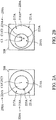
- FIGS. 2A-2B are plan views of areas 300A and 300B in FIG. 1 .
- FIGS. 2A-2B are plan views showing arrangements of a second metal pad 218A of a UBM stack 220A and a conductive plug 224A of the conductive pillar bump structure 230, and the die pad 208 of the semiconductor die 250 of the semiconductor package 500 in accordance with some embodiments of the disclosure.
- the first passivation layer 210 and the second passivation layer 212 are omitted. Because the sidewall 215 of the first metal layer 216 is aligned with the sidewall 219 of the second metal pad 218 in the cross-sectional view as shown in FIG.
- a boundary 221A of the second metal pad 218 may serve as a boundary for the UBM stack 220A in the plan view shown in FIGS. 2A-2B .
- a boundary of the conductive plug 224A may serve as a boundary for the conductive pillar bump structure 230.
- the conductive plug 224A is overlying a portion of the top surface 217A of the second metal pad 218A of the UBM stack 220A.
- the boundary 221A of the UBM stack 220A may surround the boundary 225A of the conductive plug 224A from the plan view shown in FIG. 2A or FIG. 2B .
- the boundary 221A of the UBM stack 220A may be surrounded by the boundary of the die pad 208 of the semiconductor die 250 from the plan view shown in FIG. 2A or FIG. 2B .
- an overlapping area 214A between the conductive plug 224A and the top surface 217A of the UBM stack 220A is less than the area of the top surface 217A of the UBM stack 220A.
- the die pad 208 of the semiconductor die 250 may have a central point C1
- the UBM stack 220A (or the second metal pad 218A) may have a central point C2
- the conductive plug 224A (or conductive pillar bump structure 230) may have a central point C3.
- the central point C1 of the die pad 208 overlaps the central point C2 of the UBM stack 220A (or the second metal pad 218A).
- the die pad 208 and the UBM stack 220A are concentric from the plan view shown in FIG. 2A or FIG. 2B .
- the UBM stack 220A (or 220B) (or the second metal pad 218A (or 218B)) has 2-fold rotational symmetry, which is a 180-degree rotation around the central point C2 of the UBM stack (or the second metal pad), from the plan view shown in FIG. 2A or FIG. 2B .
- the second metal pad 218A and the conductive plug 224A may be circular shapes in the plan view shown in FIGS. 2A-2B .
- the die pad 208 may be a square shape in the plan view shown in FIGS. 2A-2B .
- the central point C2 of the UBM stack 220A overlaps the central point C3 of the conductive plug 224A (or conductive pillar bump structure 230) from a plan view.
- the UBM stack 220A (or the second metal pad 218A) and the conductive plug 224A (or conductive pillar bump structure 230) are concentric from the plan view shown in FIG. 2A
- the central point C2 of the UBM stack 220A (or the second metal pad 218A) is positioned apart from the central point C3 of the conductive plug 224A (or the conductive pillar bump structure 230) by a distance S from a plan view.
- the central point C3 of the conductive plug 224A (or conductive pillar bump structure 230) is positioned apart from the central point C1 of the die pad 208 of the semiconductor die 500 by the distance S from a plan view as shown in FIG. 2B .
- the central point C3 of the conductive plug 224A may be designed to be overlapping or away from the central point C2 of the UBM stack 220A (or the second metal pad 218A) to broaden design choices.
- FIGS. 3A-3E are plan views showing shapes of second metal pads (e.g., second metal pads 218B, 218C, 218D, 218E and 218F) of UBM stacks (e.g., UBM stacks 220B, 220C, 220D, 220E and 220F) and the conductive plug 224A of the conductive pillar bump structure 230A in accordance with some embodiments of the disclosure.
- the UBM stack (or the second metal pad) may have various shapes in the plan view for design choices.
- the UBM stack stacks 220B, 220C, 220D, 220E and 220F (or the second metal pads 218B, 218C, 218D, 218E and 218F) has 2-fold rotational symmetry, which is a 180-degree rotation around the central point C2 of the UBM stack stacks 220B, 220C, 220D, 220E and 220F (or the second metal pads 218B, 218C, 218D, 218E and 218F), from plan views shown in FIGS. 3A-3E .
- the UBM stack 220B (or the second metal pad 218B) is may be an oval-shape from the plan view shown in FIG. 3A .
- the UBM stack (or the second metal pad) may have polygonal shapes from plan views shown in FIG. 3B-3D .
- the UBM stack 220C (or the second metal pad 218C) may be a square shape from the plan view shown in FIG. 3B .
- the UBM stack 220D (or the second metal pad 218D) may be a hexagonal shape from the plan view shown in FIG. 3C .
- the UBM stack 220E (or the second metal pad 218E) is may be an octagonal shape from the plan view shown in FIG. 3D .
- the UBM stack 220F (or the second metal pad 218F) is may be a rounded shape from the plan view shown in FIG. 3E .
- the die pad 208 is a square shape and the conductive plug 224A is a circular shape in the plan view shown in FIGS. 3A-3E .
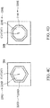
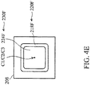
- FIGS. 4A-4E are plan views showing shapes of second metal pads (e.g., second metal pads 218B, 218C, 218D, 218E and 218F) of UBM stacks (e.g., UBM stacks 220B, 220C, 220D, 220E and 220F) and conductive plugs (e.g., conductive plugs 224B, 224C, 224D, 224E and 224F) of conductive pillar bump structures (e.g., conductive pillar bump structures 230B, 230C, 230D, 230E and 230F) in accordance with some embodiments of the disclosure.
- the conductive plug (or the conductive pillar bump structure) may have various shapes in the plan view for design choices.
- the conductive plugs 224B, 224C, 224D, 224E and 224F may be designed to have shapes that are similar to the corresponding second metal pads 218B, 218C, 218D, 218E and 218F of the UBM stacks 220B, 220C, 220D, 220E and 220F in the plan views shown FIGS. 4A-4E .
- the conductive plugs 224B, 224C, 224D, 224E and 224F (or the conductive pillar bump structures 230B, 230C, 230D, 230E and 230F) of the conductive pillar structure may be designed to have 2-fold rotational symmetry, which is a 180-degree rotation around the central point C3 of the conductive plugs 224B, 224C, 224D, 224E and 224F (or the conductive pillar bump structures 230B, 230C, 230D, 230E and 230F), in the plan views shown FIGS. 4A-4E .
- the conductive plug 224B (or the conductive pillar bump structure 230B) is may be an oval-shape from the plan view shown in FIG. 4A .
- the conductive plug (or the conductive pillar bump structure) may have polygonal shapes from the plan views shown in FIG. 4B-4D .
- the conductive plug 224C (or the conductive pillar bump structure 230C) may be a square shape from the plan view shown in FIG. 4B .
- the conductive plug 224D (or the conductive pillar bump structure 230D) may be a hexagonal shape from the plan view shown in FIG. 4C .
- the conductive plug 224E (or the conductive pillar bump structure 230E) is may be an octagonal shape from the plan view shown in FIG. 4D . Furthermore, the conductive plug 224F (or the conductive pillar bump structure 230F) is may be a rounded shape from the plan view shown in FIG. 4E . In some embodiments, the die pad 208 is a square shape in the plan view shown in FIGS. 4A-4E .
- Embodiments provide a semiconductor package, for example, a flip-chip package.
- the semiconductor package includes a semiconductor die and a conductive pillar bump structure and a conductive plug.
- the semiconductor die has a die pad thereon.
- the conductive pillar bump structure is positioned overlying the die pad.
- the conductive pillar bump structure includes an under bump metallurgy (UBM) stack having a first diameter and a conductive plug having a first diameter a second diameter that is different than the first diameter.
- UBM under bump metallurgy
- an overlapping area between the conductive plug and a top surface of the UBM stack is less than an area of the top surface of the UBM stack.
- a boundary of the UBM stack surrounds a boundary of the conductive plug from a plan view.
- the UBM stack may include a first metal layer in contact with the die pad and a second metal pad on the first metal layer.
- the second metal pad of the UBM stack and the conductive plug may be formed of copper (Cu).
- the thickness of the second metal pad is thick enough so that a top surface of the second metal pad is a planar surface (even surface).
- the second metal pad of the UBM stack may have improved mechanical strength (thick thickness and a larger diameter than the diameter of the conductive plug) to reduce the stress on the extra-low-k (ELK) dielectric layers of the semiconductor die. Therefore, the problem of cracks forming in the ELK dielectric layers can be avoided.
Landscapes
- Internal Circuitry In Semiconductor Integrated Circuit Devices (AREA)
Abstract
Description
- This application claims the benefit of
U.S. Provisional Application No. 62/458,047 filed on February 13, 2017 - The present invention relates to a semiconductor package, and in particular to a flip chip package with an improved extra-low-k (ELK) reliability.
- In order to ensure miniaturization and multi-functionality of electronic products and communication devices, semiconductor packages are required to be small in size and have multi-pin connection, high speed, and high functionality. Increased Input-Output (I/O) pin counts combined with the increased demand for high-performance ICs has led to the development of flip chip packages.
- Flip-chip technology uses bumps on the chip to interconnect the package media such as a package substrate. The flip-chip is bonded face down to the package substrate through the shortest path. These technologies can be applied not only to single-chip packaging, but also to higher or integrated levels of packaging in which the packages are larger and to more sophisticated substrates that accommodate several chips to form larger functional units. The flip-chip technique, using an area array, has the advantage of achieving a higher density of interconnection to the device and a very low inductance interconnection to the package. The increased amount of input/output connections of a multi-functional flip-chip package requires the use of extra-low-k (ELK) dielectric layers. However, the ELK dielectric layers of the chip may be susceptible to cracking due to stress. The problem of cracks forming in the ELK dielectric layers may affect the reliability and quality of the finished product.
- Thus, a novel semiconductor package is desirable.
- Exemplary embodiments of a semiconductor package are provided. An exemplary embodiment of a semiconductor package includes a semiconductor die and a conductive pillar bump structure and a conductive plug. The semiconductor die has a die pad thereon. The conductive pillar bump structure is positioned overlying the die pad. The conductive pillar bump structure includes an under bump metallurgy (UBM) stack having a first diameter and a conductive plug on the UBM stack. The conductive plug has a second diameter that is different than the first diameter.
- Another exemplary embodiment of a semiconductor package includes a semiconductor die, a conductive pillar bump structure and a conductive plug. The semiconductor die has a die pad thereon. The conductive pillar bump structure is positioned overlying the die pad. The conductive pillar bump structure includes an under bump metallurgy (UBM) stack in contact with the die pad and a conductive plug in contact with the UBM stack. An overlapping area between the conductive plug and a top surface of the UBM stack is less than an area of the top surface of the UBM stack.
- An exemplary embodiment of a semiconductor die, a conductive pillar bump structure and a conductive plug. The semiconductor die has a die pad thereon. The conductive pillar bump structure is positioned overlying the die pad. The conductive pillar bump structure includes a conductive plug and an under bump metallurgy (UBM) stack between the die pad and the conductive plug. A boundary of the UBM stack surrounds a boundary of the conductive plug from a plan view.
- A detailed description is given in the following embodiments with reference to the accompanying drawings.
- The present invention can be more fully understood by reading the subsequent detailed description and examples with references made to the accompanying drawings, wherein:
-
FIG. 1 is a cross-sectional view of a semiconductor package in accordance with some embodiments of the disclosure; -
FIGS. 2A-2B are plan views showing arrangements of a second metal pad of an under bump metallurgy (UBM) stack and a conductive plug of a conductive pillar bump structure, and a die pad of a semiconductor die of a semiconductor package in accordance with some embodiments of the disclosure; -
FIGS. 3A-3E are plan views showing shapes of second metal pads of under bump metallurgy (UBM) stacks and conductive plugs of conductive pillar bump structures in accordance with some embodiments of the disclosure; and -
FIGS. 4A-4E are plan views showing shapes of second metal pads of under bump metallurgy (UBM) stacks and conductive plugs of conductive pillar bump structures in accordance with some embodiments of the disclosure. - The following description is of the best-contemplated mode of carrying out the invention. This description is made for the purpose of illustrating the general principles of the invention and should not be taken in a limiting sense. The scope of the invention is determined by reference to the appended claims.
- The present invention will be described with respect to particular embodiments and with reference to certain drawings, but the invention is not limited thereto and is only limited by the claims. The drawings described are only schematic and are non-limiting. In the drawings, the size of some of the elements may be exaggerated for illustrative purposes and not drawn to scale. The dimensions and the relative dimensions do not correspond to actual dimensions in the practice of the invention.
-
FIG. 1 is a cross-sectional view of asemiconductor package 500 in accordance with some embodiments of the disclosure. In some embodiments, thesemiconductor package 500 is a flip-chip package using conductive pillar bumps, for example, copper pillar bumps, connecting a substrate (not shown). In some embodiments, thesemiconductor package 500 includes asemiconductor die 250 and a conductivepillar bump structure 230 electrically coupled to the semiconductor die 250. - As shown in
FIG. 1 , the semiconductor die 250 is provided. Thesemiconductor die 250 may have a back-side surface 201 and a front-side surface 203 opposite to the back-side surface 201. In some embodiments, the semiconductor die 250 includes abase 200, a diepad 208 overlying thebase 200, and afirst passivation layer 210 covering the base 240 and a portion of thedie pad 208. In some embodiments, thebase 200 may include but is not limited to a semiconductor substrate, circuit elements fabricated on the main surface of the semiconductor substrate, inter-layer dielectric (ILD) layers and an interconnection structure. For example, the interconnection structure may include a plurality of metal layers, a plurality of dielectric layers alternatively laminated with the metal layers and a plurality of vias formed through the dielectric layers on the semiconductor substrate. For example, the dielectric layers of the interconnection structure may be extra-low-k (ELK) dielectric layers. Thedie pad 208 belongs to the topmost metal layer of the metal layers of the interconnection structure. The diepad 208 may include but is not limited to aluminum (Al), copper (Cu) or alloys thereof. In some embodiments, thefirst passivation layer 210 has an opening (not shown) to expose a portion of thedie pad 208. Thefirst passivation layer 210 may include but is not limited to silicon nitride, silicon oxide, silicon oxynitride or any combination thereof. - Afterwards, a
second passivation layer 212 is formed covering thedie pad 208 and thefirst passivation layer 210, as shown inFIG. 1 in accordance with some embodiments of the disclosure. In some embodiments, thesecond passivation layer 212 is conformally formed on thefirst passivation layer 210 by a deposition process, such as a spin-on coating process, and a subsequent patterning process. Thesecond passivation layer 212 may have an opening (not shown) to expose a portion of thedie pad 208. Thesecond passivation layer 212 may include but is not limited to polyimide, polybenzoxazole (PBO) or a combination thereof. - Afterwards, the conductive
pillar bump structure 230 is formed on thedie pad 208 of the semiconductor die 250, as shown inFIG. 1 in accordance with some embodiments of the disclosure. In some embodiments, the conductivepillar bump structure 230 includes an under bump metallurgy (UBM)stack 220, aconductive plug 224 on theUBM stack 220, a solder cap 228 on theconductive plug 224, and aconductive buffer layer 226 between theconductive plug 224 and the solder cap 228. In addition, thesecond passivation layer 212 may be disposed between thefirst passivation layer 210 and the conductivepillar bump structure 230. - As shown in
FIG. 1 , an under bump metallurgy (UBM)stack 220 of the conductivepillar bump structure 230 is formed passing through thefirst passivation layer 210 and thesecond passivation layer 212 and overlying thedie pad 208. TheUBM stack 220 may be formed filling the openings of thefirst passivation layer 210 and thesecond passivation layer 212. TheUBM stack 220 may also extend onto atop surface 213 of thesecond passivation layer 212. In some embodiments, theUBM stack 220 includes afirst metal layer 216 and asecond metal pad 218 on thefirst metal layer 216. For example, thefirst metal layer 216 may be conformally formed on thefirst passivation layer 210, thesecond passivation layer 212 and thedie pad 208 in the opening. Thefirst metal layer 216 may be in contact with thedie pad 208 of the semiconductor die 250. In addition, thesecond metal pad 218 may be formed overlying thefirst metal layer 216. - In some embodiments, the
UBM stack 220 is formed by a photolithography process and subsequent electroplating processes. For example, the photolithography process may be performed to form a photoresist pattern (not shown) on thesecond passivation layer 212. The photoresist layer pattern may surrounds the openings of thefirst passivation layer 210 and thesecond passivation layer 212. The photoresist layer pattern may help to define a diameter and shape of theUBM stack 220. Next, the electroplating processes may be performed to sequentially form thefirst metal layer 216 and thesecond metal pad 218. Therefore, theUBM stack 220 may have a diameter D1 along a direction that is substantially parallel to a front-side surface 203 of the semiconductor die 250. In addition, asidewall 215 of thefirst metal layer 216 is aligned with asidewall 219 of thesecond metal pad 218. After theUBM stack 220 is formed, the photoresist pattern may be removed from thesecond passivation layer 212. - In some embodiments, the
first metal layer 216 of theUBM stack 220 is formed of titanium (Ti), and thesecond metal pad 218 of theUBM stack 220 is formed of copper (Cu). In some embodiments, the thickness T1 of thesecond metal pad 218 is much thicker than thefirst metal layer 216 of theUBM stack 220. For example, the thickness T1 of thesecond metal pad 218 may be in a range from about 0.1µm to about 10µm. Therefore, atop surface 217 of thesecond metal pad 218 may be a planar surface (even surface). When the resultingsemiconductor package 500 is bonded to a substrate, thesecond metal pad 218 of theUBM stack 220 may have improved mechanical strength (thick thickness) to reduce the stress on the extra-low-k (extra-low-dielectric constant) dielectric of the semiconductor die 250. - Afterwards, the
conductive plug 224 of the conductivepillar bump structure 230 is formed on theUBM stack 220, as shown inFIG. 1 in accordance with some embodiments of the disclosure. In some embodiments, theconductive plug 224 is formed by another photolithography process and another subsequent electroplating process. For example, the photolithography process may be performed to form a photoresist pattern (not shown) covering a portion of theUBM stack 220. The photoresist layer pattern may help to define a diameter and shape of theconductive plug 224. Next, the electroplating processes may be performed to form theconductive plug 224 on a portion of theUBM stack 220 without covered by the photoresist layer pattern. Therefore, theconductive plug 224 may have a diameter D2 along a direction that is substantially parallel to a front-side surface 203 of the semiconductor die 250. In some embodiments, theconductive plug 224 and thesecond metal pad 218 of theUBM stack 220 are formed of the same material, such as copper (Cu). In some embodiments, the diameter D1 of UBM stack 220 (or thesecond metal pad 218 of the UBM stack 220) is greater than the diameter D2 of theconductive plug 224. In some embodiments, the thickness T2 of theconductive plug 224 is thicker than the thickness T1 of thesecond metal pad 218 of theUBM stack 220. In addition, the sum of the thickness T1 of thesecond metal pad 218 and the thickness T2 of theconductive plug 224 may be kept a fixed value according the design rule. For example, the thickness T2 of theconductive plug 224 may be in a range from about 1 µm to about 20 µm (or the ratio of the thickness T2 of theconductive plug 224 to the thickness T1 of thesecond metal pad 218 may be in a range from about 1 to about 1.5). When the resultingsemiconductor package 500 is bonded to a substrate, thesecond metal pad 218 of theUBM stack 220 may have improved mechanical strength (the diameter D1 is larger than the diameter D2 of conductive plug 224) to reduce the stress on the extra-low-k (extra-low-dielectric constant) dielectric of the semiconductor die 250. - Afterwards, a
conductive buffer layer 226 formed of nickel (Ni) is formed on theconductive plug 224 by another electroplating process, as shown inFIG. 1 in accordance with some embodiments of the disclosure. In some embodiments, theconductive buffer layer 226 serve as seed layers, adhesion layers, and barrier layers for the subsequent solder cap 228 formed thereon. After theconductive plug 224 and theconductive buffer layer 226 of the conductivepillar bump structure 230 are formed, the photoresist pattern may be removed from thesecond passivation layer 212. - Afterwards, the solder cap 228 is formed on the
conductive buffer layer 226 by a photolithography process, a solder plating process, a photoresist stripping process, and a solder reflow process. After the solder cap 228 is formed, thesemiconductor package 500 is formed. -
FIGS. 2A-2B are plan views ofareas FIG. 1 .FIGS. 2A-2B are plan views showing arrangements of asecond metal pad 218A of aUBM stack 220A and aconductive plug 224A of the conductivepillar bump structure 230, and thedie pad 208 of the semiconductor die 250 of thesemiconductor package 500 in accordance with some embodiments of the disclosure. InFIGS. 2A-2B , thefirst passivation layer 210 and thesecond passivation layer 212 are omitted. Because thesidewall 215 of thefirst metal layer 216 is aligned with thesidewall 219 of thesecond metal pad 218 in the cross-sectional view as shown inFIG. 1 , aboundary 221A of thesecond metal pad 218 may serve as a boundary for theUBM stack 220A in the plan view shown inFIGS. 2A-2B . In addition, a boundary of theconductive plug 224A may serve as a boundary for the conductivepillar bump structure 230. - In some embodiments, the
conductive plug 224A is overlying a portion of thetop surface 217A of thesecond metal pad 218A of theUBM stack 220A. Theboundary 221A of theUBM stack 220A may surround theboundary 225A of theconductive plug 224A from the plan view shown inFIG. 2A or FIG. 2B . Theboundary 221A of theUBM stack 220A may be surrounded by the boundary of thedie pad 208 of the semiconductor die 250 from the plan view shown inFIG. 2A or FIG. 2B . In addition, an overlappingarea 214A between theconductive plug 224A and thetop surface 217A of theUBM stack 220A is less than the area of thetop surface 217A of theUBM stack 220A. As shown inFIGS. 2A-2B , thedie pad 208 of the semiconductor die 250 may have a central point C1, theUBM stack 220A (or thesecond metal pad 218A) may have a central point C2 and theconductive plug 224A (or conductive pillar bump structure 230) may have a central point C3. In some embodiments, the central point C1 of thedie pad 208 overlaps the central point C2 of theUBM stack 220A (or thesecond metal pad 218A). In other words, thedie pad 208 and theUBM stack 220A are concentric from the plan view shown inFIG. 2A or FIG. 2B . - In some embodiments, the
UBM stack 220A (or 220B) (or thesecond metal pad 218A (or 218B)) has 2-fold rotational symmetry, which is a 180-degree rotation around the central point C2 of the UBM stack (or the second metal pad), from the plan view shown inFIG. 2A or FIG. 2B . For example, thesecond metal pad 218A and theconductive plug 224A may be circular shapes in the plan view shown inFIGS. 2A-2B . In addition, thedie pad 208 may be a square shape in the plan view shown inFIGS. 2A-2B . - In some embodiments, as shown in
FIG. 2A , the central point C2 of theUBM stack 220A (or thesecond metal pad 218A) overlaps the central point C3 of theconductive plug 224A (or conductive pillar bump structure 230) from a plan view. In other words, theUBM stack 220A (or thesecond metal pad 218A) and theconductive plug 224A (or conductive pillar bump structure 230) are concentric from the plan view shown inFIG. 2A - In some embodiments, as shown in
FIG. 2B , the central point C2 of theUBM stack 220A (or thesecond metal pad 218A) is positioned apart from the central point C3 of theconductive plug 224A (or the conductive pillar bump structure 230) by a distance S from a plan view. In addition, the central point C3 of theconductive plug 224A (or conductive pillar bump structure 230) is positioned apart from the central point C1 of thedie pad 208 of the semiconductor die 500 by the distance S from a plan view as shown inFIG. 2B . As described previously, the central point C3 of theconductive plug 224A (or the conductive pillar bump structure 230) may be designed to be overlapping or away from the central point C2 of theUBM stack 220A (or thesecond metal pad 218A) to broaden design choices. -
FIGS. 3A-3E are plan views showing shapes of second metal pads (e.g.,second metal pads conductive plug 224A of the conductivepillar bump structure 230A in accordance with some embodiments of the disclosure. In some embodiments, the UBM stack (or the second metal pad) may have various shapes in the plan view for design choices. In some embodiments, the UBM stack stacks 220B, 220C, 220D, 220E and 220F (or thesecond metal pads second metal pads FIGS. 3A-3E . For example, theUBM stack 220B (or thesecond metal pad 218B) is may be an oval-shape from the plan view shown inFIG. 3A . In addition, the UBM stack (or the second metal pad) may have polygonal shapes from plan views shown inFIG. 3B-3D . For example, theUBM stack 220C (or thesecond metal pad 218C) may be a square shape from the plan view shown inFIG. 3B . TheUBM stack 220D (or thesecond metal pad 218D) may be a hexagonal shape from the plan view shown inFIG. 3C . TheUBM stack 220E (or thesecond metal pad 218E) is may be an octagonal shape from the plan view shown inFIG. 3D . Furthermore, theUBM stack 220F (or thesecond metal pad 218F) is may be a rounded shape from the plan view shown inFIG. 3E . In some embodiments, thedie pad 208 is a square shape and theconductive plug 224A is a circular shape in the plan view shown inFIGS. 3A-3E . -
FIGS. 4A-4E are plan views showing shapes of second metal pads (e.g.,second metal pads conductive plugs pillar bump structures pillar bump structures second metal pads FIGS. 4A-4E . In some embodiments, the conductive plugs 224B, 224C, 224D, 224E and 224F (or the conductivepillar bump structures conductive plugs pillar bump structures FIGS. 4A-4E . For example, theconductive plug 224B (or the conductivepillar bump structure 230B) is may be an oval-shape from the plan view shown inFIG. 4A . In addition, the conductive plug (or the conductive pillar bump structure) may have polygonal shapes from the plan views shown inFIG. 4B-4D . For example, theconductive plug 224C (or the conductivepillar bump structure 230C) may be a square shape from the plan view shown inFIG. 4B . Theconductive plug 224D (or the conductivepillar bump structure 230D) may be a hexagonal shape from the plan view shown inFIG. 4C . Theconductive plug 224E (or the conductivepillar bump structure 230E) is may be an octagonal shape from the plan view shown inFIG. 4D . Furthermore, theconductive plug 224F (or the conductivepillar bump structure 230F) is may be a rounded shape from the plan view shown inFIG. 4E . In some embodiments, thedie pad 208 is a square shape in the plan view shown inFIGS. 4A-4E . - Embodiments provide a semiconductor package, for example, a flip-chip package. The semiconductor package includes a semiconductor die and a conductive pillar bump structure and a conductive plug. The semiconductor die has a die pad thereon. The conductive pillar bump structure is positioned overlying the die pad. In some embodiments, the conductive pillar bump structure includes an under bump metallurgy (UBM) stack having a first diameter and a conductive plug having a first diameter a second diameter that is different than the first diameter. In some embodiments, an overlapping area between the conductive plug and a top surface of the UBM stack is less than an area of the top surface of the UBM stack. In some embodiments, a boundary of the UBM stack surrounds a boundary of the conductive plug from a plan view. The UBM stack may include a first metal layer in contact with the die pad and a second metal pad on the first metal layer. As described previously, the second metal pad of the UBM stack and the conductive plug may be formed of copper (Cu). In some embodiments, the thickness of the second metal pad is thick enough so that a top surface of the second metal pad is a planar surface (even surface). When the resulting semiconductor package is bonded to a substrate, the second metal pad of the UBM stack may have improved mechanical strength (thick thickness and a larger diameter than the diameter of the conductive plug) to reduce the stress on the extra-low-k (ELK) dielectric layers of the semiconductor die. Therefore, the problem of cracks forming in the ELK dielectric layers can be avoided.
- While the invention has been described by way of example and in terms of the preferred embodiments, it should be understood that the invention is not limited to the disclosed embodiments. On the contrary, it is intended to cover various modifications and similar arrangements (as would be apparent to those skilled in the art). Therefore, the scope of the appended claims should be accorded the broadest interpretation so as to encompass all such modifications and similar arrangements.
Claims (15)
- A semiconductor package, comprising:a semiconductor die having a die pad thereon; anda conductive pillar bump structure overlying the die pad, wherein the conductive pillar bump structure comprises:an under bump metallurgy (UBM) stack having a first diameter; anda conductive plug on the UBM stack,wherein the conductive plug has a second diameter that is different than the first diameter.
- The semiconductor package as claimed in claim 1, wherein the first diameter and the second diameter are along a direction that is substantially parallel to a front-side surface of the semiconductor die.
- The semiconductor package as claimed in claim 1 or 2, wherein the first diameter is greater than the second diameter.
- The semiconductor package as claimed in one of the preceding claims, whereinan overlapping area between the conductive plug and a top surface of the UBM stack is less than an area of the top surface of the UBM stack; and/ora boundary of the UBM stack surrounds a boundary of the conductive plug from a plan view.
- The semiconductor package as claimed in one of the preceding claims, wherein the conductive plug is overlying a portion of the top surface of the UBM stack.
- The semiconductor package as claimed in one of the preceding claims, wherein an interface between the conductive plug and the UBM stack is a planar surface.
- The semiconductor package as claimed in one of the preceding claims, wherein the UBM stack comprises:a first metal layer in contact with the die pad of the semiconductor die; anda second metal pad overlying the first metal layer and in contact with theconductive plug.
- The semiconductor package as claimed in claim 7, wherein the second metal pad and the conductive plug are formed of the same metal material.
- The semiconductor package as claimed in claim 7 or 8, whereina central point of the second metal pad overlaps a central point of the conductive plug from a plan view; and/or.a central point of the second metal pad is positioned apart from a central point of the conductive plug from a plan view; and/orthe second metal pad and the die pad of the semiconductor die are concentric from a plan view; and/ora central point of the conductive plug is positioned apart from a central point of the die pad of the semiconductor die from a plan view.
- The semiconductor package as claimed in claim 7, 8, or 9, whereinthe second metal pad has 2-fold rotational symmetry, which is a 180-degree rotation around a central point of the second metal pad, from a plan view; and/orthe second metal pad is a circular shape, an oval-shape, a polygonal shape or a rounded shape from a plan view.
- The semiconductor package as claimed in one of claims 7 to 10, wherein a first sidewall of the first metal layer is aligned with a second sidewall of the second metal pad.
- The semiconductor package as claimed in one of the preceding claims, wherein the conductive pillar bump structure comprises:a solder cap on the conductive plug; anda conductive buffer layer between the conductive plug and the solder cap.
- The semiconductor package as claimed in one of the preceding claims, wherein the semiconductor die comprises:a first passivation layer covering a portion of the die pad; anda second passivation layer disposed between the first passivation layer and the conductive pillar bump structure, on the die pad.
- A semiconductor package, comprising:a semiconductor die having a die pad thereon; anda conductive pillar bump structure overlying the die pad, wherein the conductive pillar bump structure comprises:an under bump metallurgy (UBM) stack in contact with the die pad; anda conductive plug in contact with the UBM stack,wherein an overlapping area between the conductive plug and a top surface of the UBM stack is less than an area of the top surface of the UBM stack;
wherein a central point of the UBM stack may overlap a central point of the conductive plug from a plan view. - A semiconductor package, comprising:a semiconductor die having a die pad thereon; anda conductive pillar bump structure overlying the die pad, wherein the conductive pillar bump structure comprises:a conductive plug; andan under bump metallurgy (UBM) stack between the die pad and the conductive plug,wherein a boundary of the UBM stack surrounds a boundary of the conductive plug from a plan view;
wherein the conductive plug and the second metal pad may have different shapes from the plan view.
Applications Claiming Priority (2)
| Application Number | Priority Date | Filing Date | Title |
|---|---|---|---|
| US201762458047P | 2017-02-13 | 2017-02-13 | |
| US15/881,063 US10756040B2 (en) | 2017-02-13 | 2018-01-26 | Semiconductor package with rigid under bump metallurgy (UBM) stack |
Publications (2)
| Publication Number | Publication Date |
|---|---|
| EP3361502A1 true EP3361502A1 (en) | 2018-08-15 |
| EP3361502B1 EP3361502B1 (en) | 2023-01-18 |
Family
ID=61188618
Family Applications (1)
| Application Number | Title | Priority Date | Filing Date |
|---|---|---|---|
| EP18155510.3A Active EP3361502B1 (en) | 2017-02-13 | 2018-02-07 | Semiconductor package with rigid under bump metallurgy (ubm) stack |
Country Status (3)
| Country | Link |
|---|---|
| US (1) | US10756040B2 (en) |
| EP (1) | EP3361502B1 (en) |
| TW (1) | TW201842640A (en) |
Cited By (3)
| Publication number | Priority date | Publication date | Assignee | Title |
|---|---|---|---|---|
| EP4167278A3 (en) * | 2021-09-24 | 2023-06-28 | INTEL Corporation | Methods and apparatuses with reduced defects in interconnecting bumps between a semiconductor die and a substrate (a package substrate or another die) |
| US12334422B2 (en) | 2021-09-24 | 2025-06-17 | Intel Corporation | Methods and apparatus to reduce defects in interconnects between semicondcutor dies and package substrates |
| US12616052B2 (en) | 2021-09-24 | 2026-04-28 | Intel Corporation | Methods and apparatus to reduce defects in interconnects between semicondcutor dies and package substrates |
Families Citing this family (10)
| Publication number | Priority date | Publication date | Assignee | Title |
|---|---|---|---|---|
| US11600590B2 (en) * | 2019-03-22 | 2023-03-07 | Advanced Semiconductor Engineering, Inc. | Semiconductor device and semiconductor package |
| US11211352B2 (en) * | 2019-10-01 | 2021-12-28 | Taiwan Semiconductor Manufacturing Company, Ltd. | Bump structure to prevent metal redeposit and to prevent bond pad consumption and corrosion |
| US11211301B2 (en) * | 2020-02-11 | 2021-12-28 | Taiwan Semiconductor Manufacturing Company Limited | Semiconductor device and method of manufacture |
| US11264359B2 (en) | 2020-04-27 | 2022-03-01 | Taiwan Semiconductor Manufacturing Co., Ltd. | Chip bonded to a redistribution structure with curved conductive lines |
| US12094828B2 (en) | 2020-07-17 | 2024-09-17 | Taiwan Semiconductor Manufacturing Co., Ltd. | Eccentric via structures for stress reduction |
| US11670601B2 (en) * | 2020-07-17 | 2023-06-06 | Taiwan Semiconductor Manufacturing Co., Ltd. | Stacking via structures for stress reduction |
| US12148684B2 (en) | 2020-07-31 | 2024-11-19 | Taiwan Semiconductor Manufacturing Co., Ltd. | Package structure and method |
| US12230562B2 (en) * | 2021-04-07 | 2025-02-18 | Mediatek Inc. | Three-dimensional pad structure and interconnection structure for electronic devices |
| US11955447B2 (en) * | 2021-11-17 | 2024-04-09 | Advanced Micro Devices, Inc. | Semiconductor chip having stepped conductive pillars |
| US20240282726A1 (en) * | 2023-02-17 | 2024-08-22 | Nxp Usa, Inc. | Semiconductor device with pad contact feature and method therefor |
Citations (5)
| Publication number | Priority date | Publication date | Assignee | Title |
|---|---|---|---|---|
| WO2010049087A2 (en) * | 2008-10-31 | 2010-05-06 | Advanced Micro Devices, Inc. | A semiconductor device including a reduced stress configuration for metal pillars |
| US20130075907A1 (en) * | 2011-09-23 | 2013-03-28 | Broadcom Corporation | Interconnection Between Integrated Circuit and Package |
| US8698307B2 (en) * | 2010-09-27 | 2014-04-15 | Advanced Semiconductor Engineering, Inc. | Semiconductor package with integrated metal pillars and manufacturing methods thereof |
| US20140264890A1 (en) * | 2013-03-15 | 2014-09-18 | Globalfoundries Inc. | Novel pillar structure for use in packaging integrated circuit products and methods of making such a pillar structure |
| US9425136B2 (en) * | 2012-04-17 | 2016-08-23 | Taiwan Semiconductor Manufacturing Company, Ltd. | Conical-shaped or tier-shaped pillar connections |
Family Cites Families (9)
| Publication number | Priority date | Publication date | Assignee | Title |
|---|---|---|---|---|
| US6818545B2 (en) * | 2001-03-05 | 2004-11-16 | Megic Corporation | Low fabrication cost, fine pitch and high reliability solder bump |
| JP4264823B2 (en) * | 2004-03-08 | 2009-05-20 | Okiセミコンダクタ株式会社 | Manufacturing method of semiconductor device |
| US7812438B2 (en) * | 2008-01-07 | 2010-10-12 | International Business Machines Corporation | Via offsetting to reduce stress under the first level interconnect (FLI) in microelectronics packaging |
| US8258055B2 (en) * | 2010-07-08 | 2012-09-04 | Taiwan Semiconductor Manufacturing Company, Ltd. | Method of forming semiconductor die |
| JP2012204788A (en) * | 2011-03-28 | 2012-10-22 | Renesas Electronics Corp | Semiconductor device and semiconductor device manufacturing method |
| US9105533B2 (en) * | 2011-07-27 | 2015-08-11 | Taiwan Semiconductor Manufacturing Company, Ltd. | Bump structure having a single side recess |
| US9978656B2 (en) * | 2011-11-22 | 2018-05-22 | Taiwan Semiconductor Manufacturing Company, Ltd. | Mechanisms for forming fine-pitch copper bump structures |
| CN105633046A (en) * | 2014-11-20 | 2016-06-01 | 三星电子株式会社 | Semiconductor devices and semiconductor package including same |
| KR102073294B1 (en) * | 2016-09-29 | 2020-02-04 | 삼성전자주식회사 | Fan-out semiconductor package |
-
2018
- 2018-01-26 US US15/881,063 patent/US10756040B2/en active Active
- 2018-02-07 EP EP18155510.3A patent/EP3361502B1/en active Active
- 2018-02-13 TW TW107105239A patent/TW201842640A/en unknown
Patent Citations (5)
| Publication number | Priority date | Publication date | Assignee | Title |
|---|---|---|---|---|
| WO2010049087A2 (en) * | 2008-10-31 | 2010-05-06 | Advanced Micro Devices, Inc. | A semiconductor device including a reduced stress configuration for metal pillars |
| US8698307B2 (en) * | 2010-09-27 | 2014-04-15 | Advanced Semiconductor Engineering, Inc. | Semiconductor package with integrated metal pillars and manufacturing methods thereof |
| US20130075907A1 (en) * | 2011-09-23 | 2013-03-28 | Broadcom Corporation | Interconnection Between Integrated Circuit and Package |
| US9425136B2 (en) * | 2012-04-17 | 2016-08-23 | Taiwan Semiconductor Manufacturing Company, Ltd. | Conical-shaped or tier-shaped pillar connections |
| US20140264890A1 (en) * | 2013-03-15 | 2014-09-18 | Globalfoundries Inc. | Novel pillar structure for use in packaging integrated circuit products and methods of making such a pillar structure |
Cited By (4)
| Publication number | Priority date | Publication date | Assignee | Title |
|---|---|---|---|---|
| EP4167278A3 (en) * | 2021-09-24 | 2023-06-28 | INTEL Corporation | Methods and apparatuses with reduced defects in interconnecting bumps between a semiconductor die and a substrate (a package substrate or another die) |
| US12334422B2 (en) | 2021-09-24 | 2025-06-17 | Intel Corporation | Methods and apparatus to reduce defects in interconnects between semicondcutor dies and package substrates |
| US12341117B2 (en) | 2021-09-24 | 2025-06-24 | Intel Corporation | Methods and apparatus to reduce defects in interconnects between semiconductor dies and package substrates |
| US12616052B2 (en) | 2021-09-24 | 2026-04-28 | Intel Corporation | Methods and apparatus to reduce defects in interconnects between semicondcutor dies and package substrates |
Also Published As
| Publication number | Publication date |
|---|---|
| TW201842640A (en) | 2018-12-01 |
| US10756040B2 (en) | 2020-08-25 |
| US20180233474A1 (en) | 2018-08-16 |
| EP3361502B1 (en) | 2023-01-18 |
Similar Documents
| Publication | Publication Date | Title |
|---|---|---|
| EP3361502B1 (en) | Semiconductor package with rigid under bump metallurgy (ubm) stack | |
| US20240266189A1 (en) | Semiconductor device and manufacturing method thereof | |
| US11088100B2 (en) | Semiconductor package and manufacturing method thereof | |
| US9741659B2 (en) | Electrical connections for chip scale packaging | |
| TW202133282A (en) | Semiconductor package | |
| CN108122875B (en) | Semiconductor device and semiconductor package | |
| US9105588B2 (en) | Semiconductor component having a second passivation layer having a first opening exposing a bond pad and a plurality of second openings exposing a top surface of an underlying first passivation layer | |
| CN110085523B (en) | Semiconductor device and method for manufacturing the same | |
| TWI710085B (en) | Semiconductor structure and manufacturing method thereof | |
| TWI528505B (en) | Semiconductor structure and method of manufacturing same | |
| US8703600B2 (en) | Electronic component and method of connecting with multi-profile bumps | |
| US8729700B2 (en) | Multi-direction design for bump pad structures | |
| KR20190038357A (en) | Semiconductor packages and methods of forming same | |
| US20130026658A1 (en) | Wafer level chip scale package for wire-bonding connection | |
| US20070087544A1 (en) | Method for forming improved bump structure | |
| US12469759B2 (en) | Semiconductor package | |
| CN112038329B (en) | A wafer-level chip fan-out three-dimensional stacking packaging structure and a manufacturing method thereof | |
| US9548283B2 (en) | Package redistribution layer structure and method of forming same | |
| CN110021572B (en) | Stacked package structure and its manufacturing method | |
| US20130075907A1 (en) | Interconnection Between Integrated Circuit and Package | |
| TWI711056B (en) | Conductive pattern | |
| US20240178116A1 (en) | Semiconductor package and method of manufacturing the same | |
| TWI797639B (en) | Semiconductor package and method of manufacturing semiconductor package | |
| KR20250000389A (en) | Semiconductor package and method for manufacturing the same | |
| CN106505053A (en) | Semiconductor structures and their fabrication methods |
Legal Events
| Date | Code | Title | Description |
|---|---|---|---|
| PUAI | Public reference made under article 153(3) epc to a published international application that has entered the european phase |
Free format text: ORIGINAL CODE: 0009012 |
|
| STAA | Information on the status of an ep patent application or granted ep patent |
Free format text: STATUS: THE APPLICATION HAS BEEN PUBLISHED |
|
| AK | Designated contracting states |
Kind code of ref document: A1 Designated state(s): AL AT BE BG CH CY CZ DE DK EE ES FI FR GB GR HR HU IE IS IT LI LT LU LV MC MK MT NL NO PL PT RO RS SE SI SK SM TR |
|
| AX | Request for extension of the european patent |
Extension state: BA ME |
|
| STAA | Information on the status of an ep patent application or granted ep patent |
Free format text: STATUS: REQUEST FOR EXAMINATION WAS MADE |
|
| 17P | Request for examination filed |
Effective date: 20190208 |
|
| RBV | Designated contracting states (corrected) |
Designated state(s): AL AT BE BG CH CY CZ DE DK EE ES FI FR GB GR HR HU IE IS IT LI LT LU LV MC MK MT NL NO PL PT RO RS SE SI SK SM TR |
|
| STAA | Information on the status of an ep patent application or granted ep patent |
Free format text: STATUS: EXAMINATION IS IN PROGRESS |
|
| 17Q | First examination report despatched |
Effective date: 20210608 |
|
| GRAP | Despatch of communication of intention to grant a patent |
Free format text: ORIGINAL CODE: EPIDOSNIGR1 |
|
| STAA | Information on the status of an ep patent application or granted ep patent |
Free format text: STATUS: GRANT OF PATENT IS INTENDED |
|
| RIC1 | Information provided on ipc code assigned before grant |
Ipc: H01L 23/31 20060101ALN20220713BHEP Ipc: H01L 23/29 20060101ALN20220713BHEP Ipc: H01L 23/485 20060101AFI20220713BHEP |
|
| INTG | Intention to grant announced |
Effective date: 20220808 |
|
| GRAS | Grant fee paid |
Free format text: ORIGINAL CODE: EPIDOSNIGR3 |
|
| GRAA | (expected) grant |
Free format text: ORIGINAL CODE: 0009210 |
|
| STAA | Information on the status of an ep patent application or granted ep patent |
Free format text: STATUS: THE PATENT HAS BEEN GRANTED |
|
| RAP3 | Party data changed (applicant data changed or rights of an application transferred) |
Owner name: MEDIATEK INC. |
|
| AK | Designated contracting states |
Kind code of ref document: B1 Designated state(s): AL AT BE BG CH CY CZ DE DK EE ES FI FR GB GR HR HU IE IS IT LI LT LU LV MC MK MT NL NO PL PT RO RS SE SI SK SM TR |
|
| REG | Reference to a national code |
Ref country code: GB Ref legal event code: FG4D |
|
| REG | Reference to a national code |
Ref country code: CH Ref legal event code: EP |
|
| REG | Reference to a national code |
Ref country code: DE Ref legal event code: R096 Ref document number: 602018045449 Country of ref document: DE |
|
| REG | Reference to a national code |
Ref country code: AT Ref legal event code: REF Ref document number: 1545154 Country of ref document: AT Kind code of ref document: T Effective date: 20230215 Ref country code: IE Ref legal event code: FG4D |
|
| REG | Reference to a national code |
Ref country code: LT Ref legal event code: MG9D |
|
| REG | Reference to a national code |
Ref country code: NL Ref legal event code: MP Effective date: 20230118 |
|
| REG | Reference to a national code |
Ref country code: AT Ref legal event code: MK05 Ref document number: 1545154 Country of ref document: AT Kind code of ref document: T Effective date: 20230118 |
|
| PG25 | Lapsed in a contracting state [announced via postgrant information from national office to epo] |
Ref country code: NL Free format text: LAPSE BECAUSE OF FAILURE TO SUBMIT A TRANSLATION OF THE DESCRIPTION OR TO PAY THE FEE WITHIN THE PRESCRIBED TIME-LIMIT Effective date: 20230118 |
|
| P01 | Opt-out of the competence of the unified patent court (upc) registered |
Effective date: 20230607 |
|
| PG25 | Lapsed in a contracting state [announced via postgrant information from national office to epo] |
Ref country code: RS Free format text: LAPSE BECAUSE OF FAILURE TO SUBMIT A TRANSLATION OF THE DESCRIPTION OR TO PAY THE FEE WITHIN THE PRESCRIBED TIME-LIMIT Effective date: 20230118 Ref country code: PT Free format text: LAPSE BECAUSE OF FAILURE TO SUBMIT A TRANSLATION OF THE DESCRIPTION OR TO PAY THE FEE WITHIN THE PRESCRIBED TIME-LIMIT Effective date: 20230518 Ref country code: NO Free format text: LAPSE BECAUSE OF FAILURE TO SUBMIT A TRANSLATION OF THE DESCRIPTION OR TO PAY THE FEE WITHIN THE PRESCRIBED TIME-LIMIT Effective date: 20230418 Ref country code: LV Free format text: LAPSE BECAUSE OF FAILURE TO SUBMIT A TRANSLATION OF THE DESCRIPTION OR TO PAY THE FEE WITHIN THE PRESCRIBED TIME-LIMIT Effective date: 20230118 Ref country code: LT Free format text: LAPSE BECAUSE OF FAILURE TO SUBMIT A TRANSLATION OF THE DESCRIPTION OR TO PAY THE FEE WITHIN THE PRESCRIBED TIME-LIMIT Effective date: 20230118 Ref country code: HR Free format text: LAPSE BECAUSE OF FAILURE TO SUBMIT A TRANSLATION OF THE DESCRIPTION OR TO PAY THE FEE WITHIN THE PRESCRIBED TIME-LIMIT Effective date: 20230118 Ref country code: ES Free format text: LAPSE BECAUSE OF FAILURE TO SUBMIT A TRANSLATION OF THE DESCRIPTION OR TO PAY THE FEE WITHIN THE PRESCRIBED TIME-LIMIT Effective date: 20230118 Ref country code: AT Free format text: LAPSE BECAUSE OF FAILURE TO SUBMIT A TRANSLATION OF THE DESCRIPTION OR TO PAY THE FEE WITHIN THE PRESCRIBED TIME-LIMIT Effective date: 20230118 |
|
| PG25 | Lapsed in a contracting state [announced via postgrant information from national office to epo] |
Ref country code: SE Free format text: LAPSE BECAUSE OF FAILURE TO SUBMIT A TRANSLATION OF THE DESCRIPTION OR TO PAY THE FEE WITHIN THE PRESCRIBED TIME-LIMIT Effective date: 20230118 Ref country code: PL Free format text: LAPSE BECAUSE OF FAILURE TO SUBMIT A TRANSLATION OF THE DESCRIPTION OR TO PAY THE FEE WITHIN THE PRESCRIBED TIME-LIMIT Effective date: 20230118 Ref country code: IS Free format text: LAPSE BECAUSE OF FAILURE TO SUBMIT A TRANSLATION OF THE DESCRIPTION OR TO PAY THE FEE WITHIN THE PRESCRIBED TIME-LIMIT Effective date: 20230518 Ref country code: GR Free format text: LAPSE BECAUSE OF FAILURE TO SUBMIT A TRANSLATION OF THE DESCRIPTION OR TO PAY THE FEE WITHIN THE PRESCRIBED TIME-LIMIT Effective date: 20230419 Ref country code: FI Free format text: LAPSE BECAUSE OF FAILURE TO SUBMIT A TRANSLATION OF THE DESCRIPTION OR TO PAY THE FEE WITHIN THE PRESCRIBED TIME-LIMIT Effective date: 20230118 |
|
| REG | Reference to a national code |
Ref country code: CH Ref legal event code: PL |
|
| REG | Reference to a national code |
Ref country code: DE Ref legal event code: R097 Ref document number: 602018045449 Country of ref document: DE Ref country code: BE Ref legal event code: MM Effective date: 20230228 |
|
| PG25 | Lapsed in a contracting state [announced via postgrant information from national office to epo] |
Ref country code: SM Free format text: LAPSE BECAUSE OF FAILURE TO SUBMIT A TRANSLATION OF THE DESCRIPTION OR TO PAY THE FEE WITHIN THE PRESCRIBED TIME-LIMIT Effective date: 20230118 Ref country code: RO Free format text: LAPSE BECAUSE OF FAILURE TO SUBMIT A TRANSLATION OF THE DESCRIPTION OR TO PAY THE FEE WITHIN THE PRESCRIBED TIME-LIMIT Effective date: 20230118 Ref country code: MC Free format text: LAPSE BECAUSE OF FAILURE TO SUBMIT A TRANSLATION OF THE DESCRIPTION OR TO PAY THE FEE WITHIN THE PRESCRIBED TIME-LIMIT Effective date: 20230118 Ref country code: LU Free format text: LAPSE BECAUSE OF NON-PAYMENT OF DUE FEES Effective date: 20230207 Ref country code: LI Free format text: LAPSE BECAUSE OF NON-PAYMENT OF DUE FEES Effective date: 20230228 Ref country code: EE Free format text: LAPSE BECAUSE OF FAILURE TO SUBMIT A TRANSLATION OF THE DESCRIPTION OR TO PAY THE FEE WITHIN THE PRESCRIBED TIME-LIMIT Effective date: 20230118 Ref country code: DK Free format text: LAPSE BECAUSE OF FAILURE TO SUBMIT A TRANSLATION OF THE DESCRIPTION OR TO PAY THE FEE WITHIN THE PRESCRIBED TIME-LIMIT Effective date: 20230118 Ref country code: CZ Free format text: LAPSE BECAUSE OF FAILURE TO SUBMIT A TRANSLATION OF THE DESCRIPTION OR TO PAY THE FEE WITHIN THE PRESCRIBED TIME-LIMIT Effective date: 20230118 Ref country code: CH Free format text: LAPSE BECAUSE OF NON-PAYMENT OF DUE FEES Effective date: 20230228 |
|
| PLBE | No opposition filed within time limit |
Free format text: ORIGINAL CODE: 0009261 |
|
| STAA | Information on the status of an ep patent application or granted ep patent |
Free format text: STATUS: NO OPPOSITION FILED WITHIN TIME LIMIT |
|
| PG25 | Lapsed in a contracting state [announced via postgrant information from national office to epo] |
Ref country code: SK Free format text: LAPSE BECAUSE OF FAILURE TO SUBMIT A TRANSLATION OF THE DESCRIPTION OR TO PAY THE FEE WITHIN THE PRESCRIBED TIME-LIMIT Effective date: 20230118 |
|
| REG | Reference to a national code |
Ref country code: IE Ref legal event code: MM4A |
|
| 26N | No opposition filed |
Effective date: 20231019 |
|
| PG25 | Lapsed in a contracting state [announced via postgrant information from national office to epo] |
Ref country code: SI Free format text: LAPSE BECAUSE OF FAILURE TO SUBMIT A TRANSLATION OF THE DESCRIPTION OR TO PAY THE FEE WITHIN THE PRESCRIBED TIME-LIMIT Effective date: 20230118 Ref country code: IE Free format text: LAPSE BECAUSE OF NON-PAYMENT OF DUE FEES Effective date: 20230207 |
|
| PG25 | Lapsed in a contracting state [announced via postgrant information from national office to epo] |
Ref country code: BE Free format text: LAPSE BECAUSE OF NON-PAYMENT OF DUE FEES Effective date: 20230228 |
|
| PG25 | Lapsed in a contracting state [announced via postgrant information from national office to epo] |
Ref country code: IT Free format text: LAPSE BECAUSE OF FAILURE TO SUBMIT A TRANSLATION OF THE DESCRIPTION OR TO PAY THE FEE WITHIN THE PRESCRIBED TIME-LIMIT Effective date: 20230118 |
|
| PG25 | Lapsed in a contracting state [announced via postgrant information from national office to epo] |
Ref country code: BG Free format text: LAPSE BECAUSE OF FAILURE TO SUBMIT A TRANSLATION OF THE DESCRIPTION OR TO PAY THE FEE WITHIN THE PRESCRIBED TIME-LIMIT Effective date: 20230118 |
|
| PG25 | Lapsed in a contracting state [announced via postgrant information from national office to epo] |
Ref country code: BG Free format text: LAPSE BECAUSE OF FAILURE TO SUBMIT A TRANSLATION OF THE DESCRIPTION OR TO PAY THE FEE WITHIN THE PRESCRIBED TIME-LIMIT Effective date: 20230118 |
|
| PG25 | Lapsed in a contracting state [announced via postgrant information from national office to epo] |
Ref country code: CY Free format text: LAPSE BECAUSE OF FAILURE TO SUBMIT A TRANSLATION OF THE DESCRIPTION OR TO PAY THE FEE WITHIN THE PRESCRIBED TIME-LIMIT; INVALID AB INITIO Effective date: 20180207 |
|
| PG25 | Lapsed in a contracting state [announced via postgrant information from national office to epo] |
Ref country code: HU Free format text: LAPSE BECAUSE OF FAILURE TO SUBMIT A TRANSLATION OF THE DESCRIPTION OR TO PAY THE FEE WITHIN THE PRESCRIBED TIME-LIMIT; INVALID AB INITIO Effective date: 20180207 |
|
| REG | Reference to a national code |
Ref country code: DE Ref legal event code: R079 Ref document number: 602018045449 Country of ref document: DE Free format text: PREVIOUS MAIN CLASS: H01L0023485000 Ipc: H10W0070600000 |
|
| PG25 | Lapsed in a contracting state [announced via postgrant information from national office to epo] |
Ref country code: TR Free format text: LAPSE BECAUSE OF FAILURE TO SUBMIT A TRANSLATION OF THE DESCRIPTION OR TO PAY THE FEE WITHIN THE PRESCRIBED TIME-LIMIT Effective date: 20230118 |
|
| PGFP | Annual fee paid to national office [announced via postgrant information from national office to epo] |
Ref country code: GB Payment date: 20251218 Year of fee payment: 9 |
|
| PGFP | Annual fee paid to national office [announced via postgrant information from national office to epo] |
Ref country code: FR Payment date: 20251128 Year of fee payment: 9 |
|
| PGFP | Annual fee paid to national office [announced via postgrant information from national office to epo] |
Ref country code: DE Payment date: 20251216 Year of fee payment: 9 |