EP3361486B1 - Transformer and resonant circuit having same - Google Patents
Transformer and resonant circuit having same Download PDFInfo
- Publication number
- EP3361486B1 EP3361486B1 EP16853483.2A EP16853483A EP3361486B1 EP 3361486 B1 EP3361486 B1 EP 3361486B1 EP 16853483 A EP16853483 A EP 16853483A EP 3361486 B1 EP3361486 B1 EP 3361486B1
- Authority
- EP
- European Patent Office
- Prior art keywords
- transformer
- winding
- leg
- resonant
- inductance
- Prior art date
- Legal status (The legal status is an assumption and is not a legal conclusion. Google has not performed a legal analysis and makes no representation as to the accuracy of the status listed.)
- Active
Links
Images





Classifications
-
- H—ELECTRICITY
- H01—ELECTRIC ELEMENTS
- H01F—MAGNETS; INDUCTANCES; TRANSFORMERS; SELECTION OF MATERIALS FOR THEIR MAGNETIC PROPERTIES
- H01F38/00—Adaptations of transformers or inductances for specific applications or functions
- H01F38/08—High-leakage transformers or inductances
-
- H—ELECTRICITY
- H01—ELECTRIC ELEMENTS
- H01F—MAGNETS; INDUCTANCES; TRANSFORMERS; SELECTION OF MATERIALS FOR THEIR MAGNETIC PROPERTIES
- H01F27/00—Details of transformers or inductances, in general
- H01F27/24—Magnetic cores
-
- H—ELECTRICITY
- H01—ELECTRIC ELEMENTS
- H01F—MAGNETS; INDUCTANCES; TRANSFORMERS; SELECTION OF MATERIALS FOR THEIR MAGNETIC PROPERTIES
- H01F27/00—Details of transformers or inductances, in general
- H01F27/28—Coils; Windings; Conductive connections
-
- H—ELECTRICITY
- H01—ELECTRIC ELEMENTS
- H01F—MAGNETS; INDUCTANCES; TRANSFORMERS; SELECTION OF MATERIALS FOR THEIR MAGNETIC PROPERTIES
- H01F27/00—Details of transformers or inductances, in general
- H01F27/34—Special means for preventing or reducing unwanted electric or magnetic effects, e.g. no-load losses, reactive currents, harmonics, oscillations, leakage fields
- H01F27/346—Preventing or reducing leakage fields
-
- H—ELECTRICITY
- H01—ELECTRIC ELEMENTS
- H01F—MAGNETS; INDUCTANCES; TRANSFORMERS; SELECTION OF MATERIALS FOR THEIR MAGNETIC PROPERTIES
- H01F27/00—Details of transformers or inductances, in general
- H01F27/34—Special means for preventing or reducing unwanted electric or magnetic effects, e.g. no-load losses, reactive currents, harmonics, oscillations, leakage fields
- H01F27/38—Auxiliary core members; Auxiliary coils or windings
-
- H—ELECTRICITY
- H01—ELECTRIC ELEMENTS
- H01F—MAGNETS; INDUCTANCES; TRANSFORMERS; SELECTION OF MATERIALS FOR THEIR MAGNETIC PROPERTIES
- H01F3/00—Cores, Yokes, or armatures
- H01F3/10—Composite arrangements of magnetic circuits
- H01F3/12—Magnetic shunt paths
-
- H—ELECTRICITY
- H01—ELECTRIC ELEMENTS
- H01F—MAGNETS; INDUCTANCES; TRANSFORMERS; SELECTION OF MATERIALS FOR THEIR MAGNETIC PROPERTIES
- H01F3/00—Cores, Yokes, or armatures
- H01F3/10—Composite arrangements of magnetic circuits
- H01F3/14—Constrictions; Gaps, e.g. air-gaps
-
- H—ELECTRICITY
- H02—GENERATION; CONVERSION OR DISTRIBUTION OF ELECTRIC POWER
- H02M—APPARATUS FOR CONVERSION BETWEEN AC AND AC, BETWEEN AC AND DC, OR BETWEEN DC AND DC, AND FOR USE WITH MAINS OR SIMILAR POWER SUPPLY SYSTEMS; CONVERSION OF DC OR AC INPUT POWER INTO SURGE OUTPUT POWER; CONTROL OR REGULATION THEREOF
- H02M3/00—Conversion of DC power input into DC power output
- H02M3/01—Resonant DC/DC converters
-
- H—ELECTRICITY
- H02—GENERATION; CONVERSION OR DISTRIBUTION OF ELECTRIC POWER
- H02M—APPARATUS FOR CONVERSION BETWEEN AC AND AC, BETWEEN AC AND DC, OR BETWEEN DC AND DC, AND FOR USE WITH MAINS OR SIMILAR POWER SUPPLY SYSTEMS; CONVERSION OF DC OR AC INPUT POWER INTO SURGE OUTPUT POWER; CONTROL OR REGULATION THEREOF
- H02M3/00—Conversion of DC power input into DC power output
- H02M3/22—Conversion of DC power input into DC power output with intermediate conversion into AC
- H02M3/24—Conversion of DC power input into DC power output with intermediate conversion into AC by static converters
- H02M3/28—Conversion of DC power input into DC power output with intermediate conversion into AC by static converters using discharge tubes with control electrode or semiconductor devices with control electrode to produce the intermediate AC
- H02M3/325—Conversion of DC power input into DC power output with intermediate conversion into AC by static converters using discharge tubes with control electrode or semiconductor devices with control electrode to produce the intermediate AC using devices of a triode or a transistor type requiring continuous application of a control signal
- H02M3/335—Conversion of DC power input into DC power output with intermediate conversion into AC by static converters using discharge tubes with control electrode or semiconductor devices with control electrode to produce the intermediate AC using devices of a triode or a transistor type requiring continuous application of a control signal using semiconductor devices only
- H02M3/33569—Conversion of DC power input into DC power output with intermediate conversion into AC by static converters using discharge tubes with control electrode or semiconductor devices with control electrode to produce the intermediate AC using devices of a triode or a transistor type requiring continuous application of a control signal using semiconductor devices only having several active switching elements
- H02M3/33571—Half-bridge at primary side of an isolation transformer
-
- H—ELECTRICITY
- H02—GENERATION; CONVERSION OR DISTRIBUTION OF ELECTRIC POWER
- H02M—APPARATUS FOR CONVERSION BETWEEN AC AND AC, BETWEEN AC AND DC, OR BETWEEN DC AND DC, AND FOR USE WITH MAINS OR SIMILAR POWER SUPPLY SYSTEMS; CONVERSION OF DC OR AC INPUT POWER INTO SURGE OUTPUT POWER; CONTROL OR REGULATION THEREOF
- H02M1/00—Details of apparatus for conversion
- H02M1/0048—Circuits or arrangements for reducing losses
- H02M1/0054—Transistor switching losses
- H02M1/0058—Transistor switching losses by employing soft switching techniques, i.e. commutation of transistors when applied voltage is zero or when current flow is zero
-
- H—ELECTRICITY
- H02—GENERATION; CONVERSION OR DISTRIBUTION OF ELECTRIC POWER
- H02M—APPARATUS FOR CONVERSION BETWEEN AC AND AC, BETWEEN AC AND DC, OR BETWEEN DC AND DC, AND FOR USE WITH MAINS OR SIMILAR POWER SUPPLY SYSTEMS; CONVERSION OF DC OR AC INPUT POWER INTO SURGE OUTPUT POWER; CONTROL OR REGULATION THEREOF
- H02M1/00—Details of apparatus for conversion
- H02M1/0064—Magnetic structures combining different functions, e.g. storage, filtering or transformation
-
- H—ELECTRICITY
- H02—GENERATION; CONVERSION OR DISTRIBUTION OF ELECTRIC POWER
- H02M—APPARATUS FOR CONVERSION BETWEEN AC AND AC, BETWEEN AC AND DC, OR BETWEEN DC AND DC, AND FOR USE WITH MAINS OR SIMILAR POWER SUPPLY SYSTEMS; CONVERSION OF DC OR AC INPUT POWER INTO SURGE OUTPUT POWER; CONTROL OR REGULATION THEREOF
- H02M3/00—Conversion of DC power input into DC power output
- H02M3/003—Constructional details, e.g. physical layout, assembly, wiring or busbar connections
-
- Y—GENERAL TAGGING OF NEW TECHNOLOGICAL DEVELOPMENTS; GENERAL TAGGING OF CROSS-SECTIONAL TECHNOLOGIES SPANNING OVER SEVERAL SECTIONS OF THE IPC; TECHNICAL SUBJECTS COVERED BY FORMER USPC CROSS-REFERENCE ART COLLECTIONS [XRACs] AND DIGESTS
- Y02—TECHNOLOGIES OR APPLICATIONS FOR MITIGATION OR ADAPTATION AGAINST CLIMATE CHANGE
- Y02B—CLIMATE CHANGE MITIGATION TECHNOLOGIES RELATED TO BUILDINGS, e.g. HOUSING, HOUSE APPLIANCES OR RELATED END-USER APPLICATIONS
- Y02B70/00—Technologies for an efficient end-user side electric power management and consumption
- Y02B70/10—Technologies improving the efficiency by using switched-mode power supplies [SMPS], i.e. efficient power electronics conversion e.g. power factor correction or reduction of losses in power supplies or efficient standby modes
Definitions
- the present invention relates to a small transformer (a transformer) having a high leakage inductance used in a resonant circuit, and a resonant circuit having the same.
- a resonant circuit realizes soft switching using the resonance of a resonant inductance Lr and a resonant capacitor Cr.
- a leakage inductance of a transformer can be used in the resonant inductance Lr. It is known that, with use of the leakage inductance, the number of parts is reduced, and noise can be reduced.
- the leakage magnetic field from the added magnet intersects with the surrounding windings, and thereby a loss is increased. Since the magnet is additionally required, there are more members.
- US 2008/224809 A1 discloses, in one example, a transformer comprising a double E core with sections of the primary winding with different winding number being wound on the side legs of the core and with a secondary winding wound on one of the side legs.
- the middle leg has a greater cross section than the side legs and is without winding.
- BO YANG ET AL "Integrated magnetic for LLC resonant converter"
- APEC 2002 17th ANNUAL IEEE APPLIED POWER ELECTRONICS CONFERENCE AND EXPOSITION, March 10, 2002, pages 346-351 discloses a LLC resonant converter for front end DC/DC conversion in a distributed power system.
- this paper discloses a tranformer structure similar to US 2008/224809 A1 .
- FR 1 398 708 A discloses a static transformer which can operate as normal transformer or magnetic leakage transformer.
- the magnetic core of the transformer comprises three parallel legs. A first side leg is wound with primary and secondary windings, the middle leg is wound only with a primary winding section and the second side leg is free of windings and has a smaller cross section than the other core legs.
- US 4 328 458 A discloses a variable leakage transformer having a closed main magnetic path and a closed submagnetic path having a leg common with said main magnetic path.
- a primary winding is wound on said common leg, and a secondary winding is wound on said main magnetic path.
- the magnetic flux in the common leg is controlled by other control windings which are connected to a control DC power source.
- the primary winding has two portions, and one of them is closely coupled magnetically with the secondary winding in order to improve the output waveform.
- the magnetic core comprises three parallel legs with the primary windings being wound around a side leg and the middle leg and the secondary winding being wound around the side leg with the primary winding.
- an object of the present invention is to provide a transformer that obtains a high leakage inductance by generating magnetic fluxes having a sufficient difference in magnitude at two positions in a core due to primary windings, and a resonant circuit having this transformer.
- the core has a path of the magnetic flux, which does not intersect with the secondary winding, of the first magnetic flux and the second magnetic flux which are generated by the primary windings. Further, a gap may be provided in the path.
- the transformer having this configuration a small transformer in which an additional member is not required, a loss caused by an influence of a leakage magnetic field or a proximity effect is not also increased, and a high leakage inductance is obtained can be realized.
- the leakage inductance can be arbitrarily adjusted by a length of this gap.
- At least one of a cross-sectional area or the number of turns of the primary winding may differ at the first winding leg and the second winding leg.
- a gap may be provided in either the first winding leg or the second winding leg, or gaps having different lengths may be respectively provided in the first winding leg and the second winding leg.
- the present invention is not limited to this method.
- a resonant circuit of the present invention is characterized in including: the transformer, a resonant inductance, and a resonant capacitor, the resonant circuit uses resonance of the resonant inductance and the resonant capacitor connected to an excitation inductance of the transformer.
- the resonant inductance and the resonant capacitor may be connected in series to the excitation inductance.
- a ratio between the excitation inductance and the resonant inductance is preferably less than or equal to 3.
- the transformer of the present invention a small transformer in which an additional member is not required, a loss caused by an influence of a leakage magnetic field or a proximity effect is not also increased, and a high leakage inductance is obtained can be realized.
- Fig. 1 is an overview configuration diagram of a transformer 1 according to a first embodiment of the present invention.
- Fig. 2(a) is a schematic explanatory diagram of an excitation inductance Lm and a leakage inductance Llk in the transformer 1.
- Fig. 2(b) is a schematic explanatory diagram of an example in which a gap is provided in a left leg 10c of a core 10 of the transformer 1.
- the transformer 1 includes a core 10 that forms a magnetic circuit, primary windings 11 that are input sides, and a secondary first winding 12a and a secondary second winding 12b (referred to collectively as a secondary winding 12) that are output sides.
- a secondary winding 12 a secondary first winding 12a and a secondary second winding 12b
- a center tap is removed from the secondary winding 12
- only one of the secondary first winding 12a and the secondary second winding 12b may be used.
- the core 10 has one middle leg 10a and side legs lOb and 10c branching off into two from the middle leg 10a (distinguished by being called a right leg 10b and a left leg 10c as needed), and is made up of, for instance, an E type core and an I type core, or E type cores, or the like.
- a material of the core 10 may be a typical material.
- the primary windings 11 are wound around two legs that are the middle leg 10a and one of the side legs 10b and 10c (which are a "first winding leg” and a “second winding leg” in this application, and the middle leg 10a and the right leg 10b herein) with winding directions (indicated by arrows superimposed on the primary windings 11 in the figure) opposite to each other.
- the middle leg 10a and the right leg lOb are selected will be described by way of example.
- a combination of the two legs may be the left leg 10c and the middle leg 10a.
- the secondary winding 12 is wound around any one of the selected two legs, that is, the middle leg 10a and the right leg 10b (here, the right leg 10b).
- a PCB board on which a pattern is formed for instance a PCB board on which a pattern is formed (a pattern coil), an edgewise coil, or a copper foil may be used as a wire, in addition to a litz wire obtained by twisting fine wires and a single wire, but the present invention is not limited thereto.
- the bobbin may be used together.
- the leakage inductance Llk can be arbitrarily adjusted by a length Gc of this gap.
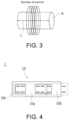
- Fig. 3 is an explanatory diagram of parameters relevant to permeance P used in magnetic circuit calculation.
- Total magnetic flux ⁇ Magnetomotive force F / Magnetic resistance R
- Total magnetic flux ⁇ Magnetomotive force F / Magnetic resistance R
- this permeance P is expressed by the following formula when a magnetic path length is defined as L, a magnetic path cross-sectional area is defined as A, and permeability is defined as ⁇ .
- Permeance P Permeability ⁇ ⁇ Magnetic path cross-sectional area A / Magnetic path length L
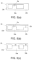
- Fig. 4 is a schematic explanatory diagram of a method for giving a difference to a magnetomotive force F in the transformer 1.
- Fig. 5(a) to Fig. 5(c) are schematic explanatory diagrams of a method for giving a difference to magnetic resistance R in the transformer 1.
- a difference may be given to magnetomotive forces F of the middle leg 10a and the right leg 10b of the transformer 1.
- the magnetomotive force F is expressed by the following formula, it is considered, for instance, to make the middle leg 10a and the right leg 10b different in the number of turns N from each other as illustrated in Fig. 4 .
- a difference may be given to the magnetic resistance R of each of the portions around which the primary windings 11 are wound in the core 10 of the transformer 1, particularly the middle leg 10a and the right leg 10b here.
- a gap may be provided for at least one of the middle leg 10a and the right leg 10b, or illustrated in Fig. 5(b) , when the gap is provided for both of them, a length of each gap may be changed. Since the gap portion and the core 10 are different in permeability ⁇ from each other, the permeability ⁇ at large is changed depending on the length of the gap.
- the gap is not necessarily provided at an upper side of the core 10 as illustrated in Fig. 5(a) and Fig. 5(b) , and it may be provided for each of the middle leg 10a and the right leg 10b.
- magnetic path cross-sectional areas Aa and Ab of the middle leg 10a and the right leg 10b may be made different from each other.
- the present invention is not limited to these methods.
- the small transformer in which an additional member such as a magnet is not required, a loss caused when a leakage magnetic field intersects with its surrounding windings is not also increased, a reduction in efficiency caused by a proximity effect generated when the number of layers of the primary winding is increased is not also incurred, and a high leakage inductance is obtained can be realized.
- Fig. 6(a) and Fig. 6(b) are schematic diagrams illustrating other winding methods of the primary windings 11 and the secondary winding 12 (12a and 12b).
- Fig. 7(a) to Fig. 7(c) are schematic diagrams illustrating still other winding methods of the primary windings 11 and the secondary winding 12 (12a and 12b).
- the primary windings 11 are wound around the middle leg 10a and the right leg 10b with the winding directions opposite to each other.
- the secondary winding 12 (the secondary first winding 12a and the secondary second winding 12b) is wound around the right leg 10b below the primary windings 11.
- the winding methods of the primary windings 11 and the secondary winding 12 are not limited thereto.
- the primary windings 11 and the secondary winding 12 may be alternately wound.
- the primary winding 11, the secondary winding 12 (the secondary first winding 12a), the secondary winding 12 (the secondary second winding 12b), and the primary winding 11 may be wound from above in this order.
- the winding methods of the primary windings 11 and the secondary winding 12 in the first embodiment may be turned upside down as illustrated in Fig. 7(a) .
- the winding methods illustrated in Fig. 6(a) may also be turned upside down as illustrated in Fig. 7(b) .
- the winding methods illustrated in Fig. 6(b) may also be turned upside down as illustrated in Fig. 7(c) .
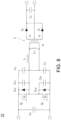
- Fig. 8 is an overview configuration diagram of a half bridge type series resonant converter circuit 20 according to a second embodiment of the present invention.
- the transformer 1 of the aforementioned first embodiment is suitable for, for instance, series resonant converter circuits of a half bridge and a full bridge, a phase shift full bridge circuit, a dual active bridge (DAB) circuit, or the like.
- DAB dual active bridge
- a resonant circuit that uses the resonance of a resonant inductance Lr and a resonant capacitor Cr which are connected in series to an excitation inductance of the transformer 1.
- An example of the resonant circuit is the half bridge type series resonant converter circuit 20 illustrated in Fig. 8 .
- the half bridge type series resonant converter circuit 20 includes a capacitor C in , a capacitor C Q1 , a capacitor C r1 , a capacitor C Q2 , a capacitor C r2 , a capacitor C d , a transistor Q 1 , a transistor Q 2 , a diode D Q1 , a diode D Q2 , a diode D 1 , a diode D 2 , a primary winding n 1 , a secondary winding n 2 and a secondary winding n 3 .
- Fig. 9 is an overview configuration diagram of a core 10 of a first example of the first embodiment of the present invention.
- a core 10 was used in which a cross-sectional area Ac of the left leg 10c for a leakage inductance path was set to 1, a cross-sectional area Aa of the middle leg 10a was set to 2, and a cross-sectional area Ab of the right leg 10b was set to 2.
- the primary winding 11 was alternately wound around the middle leg 10a and the right leg 10b of the core 10 in the number 8 by two turns for the middle leg and one turn for the right leg for a total of 15 turns (ten turns of the middle leg and five turns for the right leg), and finally one turn for the right leg.
- the secondary winding 12 was wound around the right leg 10b of the core 10 in the same direction as the primary winding 11 by two turns, and aside from this, the secondary winding 12 was wound around the right leg 10b in the direction opposite to the direction of the primary winding 11 by two turns.
- Measurement was performed using an LCR meter.
- a measurement condition was a frequency of 100 kHz.
- the secondary winding 12 was opened, and an inductance value Lp of the primary winding 11 was measured.
- the secondary winding 12 was shorted, and the inductance Llk of the primary winding 11 was measured.
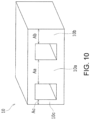
- Fig. 10 is an overview configuration diagram of a core 10 of a second example of the first embodiment of the present invention.
- a core 10 was used in which a cross-sectional area Ac of the left leg 10c for a leakage inductance path was set to 1, a cross-sectional area Aa of the middle leg 10a was set to 3, and a cross-sectional area Ab of the right leg 10b was set to 2.
- the primary winding 11 was alternately wound around the middle leg 10a and the right leg 10b of the core 10 in the number 8 by one turn after another for a total of 16 turns (eight turns of the middle leg and eight turns for the right leg).
- the secondary winding 12 was wound around the right leg 10b of the core 10 in the same direction as the primary winding 11 by two turns, and aside from this, the secondary winding 12 was wound around the right leg 10b in the direction opposite to the direction of the primary winding 11 by two turns.
- a measurement device, a measurement condition, and a measuring method were the same as in the first example. Measured results were as follows.
- Fig. 11 is an overview configuration diagram of a core 10 of a third example of the first embodiment of the present invention.
- a core 10 was used in which a cross-sectional area Ac of the left leg 10c for a leakage inductance path was set to 1, a cross-sectional area Aa of the middle leg 10a was set to 2, and a cross-sectional area Ab of the right leg 10b was set to 2, and in which a length Ga of the gap of the middle leg 10a was set to 1, and a length Gb of the gap of the right leg 10b was set to 2.
- the primary winding 11 was alternately wound around the middle leg 10a and the right leg 10b of the core 10 in the number 8 by one turn after another for a total of 16 turns (eight turns of the middle leg and eight turns for the right leg).
- the secondary winding 12 was wound around the right leg 10b of the core 10 in the same direction as the primary winding 11 by two turns, and aside from this, the secondary winding 12 was wound around the right leg 10b in the direction opposite to the direction of the primary winding 11 by two turns.
- a measurement device, a measurement condition, and a measuring method were the same as in the first example. Measured results were as follows.
- the configurations of the first embodiment, its modification, the second embodiment, and the first to third examples which are described above may be combined with one another as long as obstructive factors or the like are not especially present.
Landscapes
- Engineering & Computer Science (AREA)
- Power Engineering (AREA)
- Chemical & Material Sciences (AREA)
- Composite Materials (AREA)
- Dc-Dc Converters (AREA)
- Coils Of Transformers For General Uses (AREA)
- Coils Or Transformers For Communication (AREA)
Description
- The present invention relates to a small transformer (a transformer) having a high leakage inductance used in a resonant circuit, and a resonant circuit having the same.
- Conventionally, a resonant circuit realizes soft switching using the resonance of a resonant inductance Lr and a resonant capacitor Cr. A leakage inductance of a transformer can be used in the resonant inductance Lr. It is known that, with use of the leakage inductance, the number of parts is reduced, and noise can be reduced.
- However, when a transformer is made smaller, there is a problem that it is difficult to maintain a sufficient interval between a primary winding and a secondary winding for making leakage inductance, and a leakage inductance required for resonance may not be obtained.
- Thus, to obtain a high leakage inductance, a method using a bobbin that separates a primary winding from a secondary winding has been proposed (e.g., see Patent Literature 1).
- However, to obtain a sufficient leakage inductance, it is necessary to increase a separation distance between the primary winding and the secondary winding, and the transformer is made larger.
- To increase the leakage inductance of the transformer, a method of generating a leakage magnetic field to obtain a high leakage inductance by adding a magnet between the primary winding and the secondary winding has also been proposed (e.g., see Patent Literature 2).
- However, the leakage magnetic field from the added magnet intersects with the surrounding windings, and thereby a loss is increased. Since the magnet is additionally required, there are more members.
- A method for obtaining a leakage inductance by winding a secondary winding around a middle leg portion around which a primary winding is wound and side legs around which the primary winding is not wound has been proposed (e.g., see Patent Literature 3).
- However, in the method in which the primary winding is wound around the middle leg portion alone, the number of layers of the primary winding is increased, and efficiency is reduced by a proximity effect.
-
- [Patent Literature 1]
Japanese Unexamined Patent Application Publication No. 2001-237126 - [Patent Literature 2]
Japanese Unexamined Patent Application Publication No. 2013-172135 - [Patent Literature 3]
Japanese Unexamined Patent Application Publication No. 2008-166624 -
US 2008/224809 A1 discloses, in one example, a transformer comprising a double E core with sections of the primary winding with different winding number being wound on the side legs of the core and with a secondary winding wound on one of the side legs. The middle leg has a greater cross section than the side legs and is without winding. - BO YANG ET AL: "Integrated magnetic for LLC resonant converter", APEC 2002, 17th ANNUAL IEEE APPLIED POWER ELECTRONICS CONFERENCE AND EXPOSITION, March 10, 2002, pages 346-351 discloses a LLC resonant converter for front end DC/DC conversion in a distributed power system. In one example, this paper discloses a tranformer structure similar to
US 2008/224809 A1 . -
FR 1 398 708 A -
US 4 328 458 A discloses a variable leakage transformer having a closed main magnetic path and a closed submagnetic path having a leg common with said main magnetic path. A primary winding is wound on said common leg, and a secondary winding is wound on said main magnetic path. The magnetic flux in the common leg is controlled by other control windings which are connected to a control DC power source. The primary winding has two portions, and one of them is closely coupled magnetically with the secondary winding in order to improve the output waveform. In one embodiment, the magnetic core comprises three parallel legs with the primary windings being wound around a side leg and the middle leg and the secondary winding being wound around the side leg with the primary winding. - In view of these problems of the related art, an object of the present invention is to provide a transformer that obtains a high leakage inductance by generating magnetic fluxes having a sufficient difference in magnitude at two positions in a core due to primary windings, and a resonant circuit having this transformer.
- To achieve the above object, the present invention is provided in appended
claim 1.. - Here, the core has a path of the magnetic flux, which does not intersect with the secondary winding, of the first magnetic flux and the second magnetic flux which are generated by the primary windings. Further, a gap may be provided in the path.
- According to the transformer having this configuration, a small transformer in which an additional member is not required, a loss caused by an influence of a leakage magnetic field or a proximity effect is not also increased, and a high leakage inductance is obtained can be realized. When the gap is provided in the path, the leakage inductance can be arbitrarily adjusted by a length of this gap.
- In the transformer of the present invention, to give a difference to magnitudes of the first magnetic flux and the second magnetic flux, for example, at least one of a cross-sectional area or the number of turns of the primary winding may differ at the first winding leg and the second winding leg. Alternatively, a gap may be provided in either the first winding leg or the second winding leg, or gaps having different lengths may be respectively provided in the first winding leg and the second winding leg. However, the present invention is not limited to this method.
- A resonant circuit of the present invention is characterized in including: the transformer, a resonant inductance, and a resonant capacitor, the resonant circuit uses resonance of the resonant inductance and the resonant capacitor connected to an excitation inductance of the transformer. The resonant inductance and the resonant capacitor may be connected in series to the excitation inductance.
- According to the resonant circuit having this configuration, a resonant converter or a series resonant converter in which a ratio (I=Lm/Lr) between the excitation inductance (Lm) and the resonant inductance (Lr) is small can be configured. Since a frequency characteristic is sharp, a wide range of output voltage can be obtained by changing a switching frequency or, when the output voltage is constantly controlled, an input range can be widened by changing a switching frequency.
- When the resonant circuit of the present invention is an LLC type resonant circuit, a ratio between the excitation inductance and the resonant inductance is preferably less than or equal to 3.
- According to the transformer of the present invention, a small transformer in which an additional member is not required, a loss caused by an influence of a leakage magnetic field or a proximity effect is not also increased, and a high leakage inductance is obtained can be realized.
- According to the resonant circuit having the transformer of the present invention, a series resonant converter in which a ratio (I=Lm/Lr) between the excitation inductance (Lm) and the resonant inductance (Lr) is small can be configured. Since a frequency characteristic is sharp, a wide range of output voltage can be obtained by changing a switching frequency or, when the output voltage is constantly controlled, an input range can be widened by changing a switching frequency.
-
-
Fig. 1 is an overview configuration diagram of atransformer 1 according to a first embodiment of the present invention. -
Fig. 2(a) is a schematic explanatory diagram of an excitation inductance Lm and a leakage inductance Llk in thetransformer 1, andFig. 2(b) is a schematic explanatory diagram of an example in which a gap is provided in aleft leg 10c of acore 10 of thetransformer 1. -
Fig. 3 is an explanatory diagram of parameters relevant to permeance P used in a magnetic circuit calculation. -
Fig. 4 is a schematic explanatory diagram of a method for giving a difference to a magnetomotive force F in thetransformer 1. -
Fig. 5(a) to Fig. 5(c) are schematic explanatory diagrams of a method for giving a difference to magnetic resistance R in thetransformer 1. -
Fig. 6(a) and Fig. 6(b) are schematic diagrams illustrating other winding methods ofprimary windings 11 and a secondary winding 12 (12a and 12b). -
Fig. 7(a) to Fig. 7(c) are schematic diagrams illustrating still other winding methods of theprimary windings 11 and the secondary winding 12 (12a and 12b). -
Fig. 8 is an overview configuration diagram of a seriesresonant converter circuit 20 according to a second embodiment of the present invention. -
Fig. 9 is an overview configuration diagram of acore 10 of a first example of the first embodiment of the present invention. -
Fig. 10 is an overview configuration diagram of acore 10 of a second example of the first embodiment of the present invention. -
Fig. 11 is an overview configuration diagram of acore 10 of a third example of the first embodiment of the present invention. - Hereinafter, several embodiments of the present invention will be described on the basis of the drawings.
-
Fig. 1 is an overview configuration diagram of atransformer 1 according to a first embodiment of the present invention.Fig. 2(a) is a schematic explanatory diagram of an excitation inductance Lm and a leakage inductance Llk in thetransformer 1.Fig. 2(b) is a schematic explanatory diagram of an example in which a gap is provided in aleft leg 10c of acore 10 of thetransformer 1. - As illustrated in
Fig. 1 , thetransformer 1 includes a core 10 that forms a magnetic circuit,primary windings 11 that are input sides, and a secondary first winding 12a and a secondary second winding 12b (referred to collectively as a secondary winding 12) that are output sides. Here, a case in which a center tap is removed from the secondary winding 12 is shown, but if the center tap is not removed, only one of the secondary first winding 12a and the secondary second winding 12b may be used. - The
core 10 has onemiddle leg 10a and side legs lOb and 10c branching off into two from themiddle leg 10a (distinguished by being called aright leg 10b and aleft leg 10c as needed), and is made up of, for instance, an E type core and an I type core, or E type cores, or the like. A material of the core 10 may be a typical material. - The
primary windings 11 are wound around two legs that are themiddle leg 10a and one of theside legs middle leg 10a and theright leg 10b herein) with winding directions (indicated by arrows superimposed on theprimary windings 11 in the figure) opposite to each other. Hereinafter, the case in which themiddle leg 10a and the right leg lOb are selected will be described by way of example. However, a combination of the two legs may be theleft leg 10c and themiddle leg 10a. - The secondary winding 12 is wound around any one of the selected two legs, that is, the
middle leg 10a and theright leg 10b (here, theright leg 10b). - For the
primary windings 11 and the secondary winding 12, for instance a PCB board on which a pattern is formed (a pattern coil), an edgewise coil, or a copper foil may be used as a wire, in addition to a litz wire obtained by twisting fine wires and a single wire, but the present invention is not limited thereto. When the wire is used, the bobbin may be used together. - In the configuration of this
transformer 1, as illustrated inFig. 2(a) , if magnetic fluxes Φa and Φb are generated at the two legs (here, themiddle leg 10a and theright leg 10b) around which theprimary windings 11 are wound, and a sufficient difference (a difference that is greater than or equal to a predetermined given value) in the magnitudes of the magnetic fluxes Φa and Φb is present at positions at which the magnetic fluxes do not intersect with the secondary winding 12, the secondary winding 12 is wound around only one of themiddle leg 10a and theright leg 10b, and thecore 10 has a path (theleft leg 10c) flowing the leakage inductance Llk. Thus, a high leakage inductance Llk can be obtained. - As illustrated in
Fig. 2(b) , when a gap is provided in the path flowing the leakage inductance Llk in thecore 10 of thetransformer 1, the leakage inductance Llk can be arbitrarily adjusted by a length Gc of this gap. -
Fig. 3 is an explanatory diagram of parameters relevant to permeance P used in magnetic circuit calculation. - Next, an example of a method for giving a difference to the magnitudes of the generated magnetic fluxes will be described, but a basis of the magnetic circuit calculation is checked first. Total magnetic flux Φ, a magnetomotive force F, and magnetic resistance R has a relation of the following formula.


Fig. 3 , this permeance P is expressed by the following formula when a magnetic path length is defined as L, a magnetic path cross-sectional area is defined as A, and permeability is defined as µ.

Fig. 4 is a schematic explanatory diagram of a method for giving a difference to a magnetomotive force F in thetransformer 1.Fig. 5(a) to Fig. 5(c) are schematic explanatory diagrams of a method for giving a difference to magnetic resistance R in thetransformer 1. - As an example of the method for giving the difference to the magnitudes of the generated magnetic fluxes, a difference may be given to magnetomotive forces F of the
middle leg 10a and theright leg 10b of thetransformer 1. - Since the magnetomotive force F is expressed by the following formula, it is considered, for instance, to make the
middle leg 10a and theright leg 10b different in the number of turns N from each other as illustrated inFig. 4 . - As another example of the method for giving the difference to the magnitudes of the generated magnetic fluxes, a difference may be given to the magnetic resistance R of each of the portions around which the
primary windings 11 are wound in thecore 10 of thetransformer 1, particularly themiddle leg 10a and theright leg 10b here. - As can be seen from formula (3) above, since the permeability µ, the magnetic path cross-sectional area A, and the magnetic path length L are relevant to the permeance P (the reciprocal of the magnetic resistance R), at least one of these parameters needs only to be changed.
- For example, as illustrated in
Fig. 5(a) , a gap may be provided for at least one of themiddle leg 10a and theright leg 10b, or illustrated inFig. 5(b) , when the gap is provided for both of them, a length of each gap may be changed. Since the gap portion and the core 10 are different in permeability µ from each other, the permeability µ at large is changed depending on the length of the gap. The gap is not necessarily provided at an upper side of the core 10 as illustrated inFig. 5(a) and Fig. 5(b) , and it may be provided for each of themiddle leg 10a and theright leg 10b. - As illustrated in
Fig. 5(c) , magnetic path cross-sectional areas Aa and Ab of themiddle leg 10a and theright leg 10b may be made different from each other. However, the present invention is not limited to these methods. - According to the first embodiment described above, the small transformer in which an additional member such as a magnet is not required, a loss caused when a leakage magnetic field intersects with its surrounding windings is not also increased, a reduction in efficiency caused by a proximity effect generated when the number of layers of the primary winding is increased is not also incurred, and a high leakage inductance is obtained can be realized.
-
Fig. 6(a) and Fig. 6(b) are schematic diagrams illustrating other winding methods of theprimary windings 11 and the secondary winding 12 (12a and 12b).Fig. 7(a) to Fig. 7(c) are schematic diagrams illustrating still other winding methods of theprimary windings 11 and the secondary winding 12 (12a and 12b). - In the aforementioned first embodiment, the
primary windings 11 are wound around themiddle leg 10a and theright leg 10b with the winding directions opposite to each other. The secondary winding 12 (the secondary first winding 12a and the secondary second winding 12b) is wound around theright leg 10b below theprimary windings 11. However, the winding methods of theprimary windings 11 and the secondary winding 12 are not limited thereto. - For example, as illustrated in
Fig. 6(a) , theprimary windings 11 and the secondary winding 12 may be alternately wound. Alternatively, as illustrated inFig. 6(b) , the primary winding 11, the secondary winding 12 (the secondary first winding 12a), the secondary winding 12 (the secondary second winding 12b), and the primary winding 11 may be wound from above in this order. - The winding methods of the
primary windings 11 and the secondary winding 12 in the first embodiment may be turned upside down as illustrated inFig. 7(a) . The winding methods illustrated inFig. 6(a) may also be turned upside down as illustrated inFig. 7(b) . Likewise, the winding methods illustrated inFig. 6(b) may also be turned upside down as illustrated inFig. 7(c) . -
Fig. 8 is an overview configuration diagram of a half bridge type seriesresonant converter circuit 20 according to a second embodiment of the present invention. - The
transformer 1 of the aforementioned first embodiment is suitable for, for instance, series resonant converter circuits of a half bridge and a full bridge, a phase shift full bridge circuit, a dual active bridge (DAB) circuit, or the like. - It can be used in a resonant circuit that uses the resonance of a resonant inductance Lr and a resonant capacitor Cr which are connected in series to an excitation inductance of the
transformer 1. An example of the resonant circuit is the half bridge type seriesresonant converter circuit 20 illustrated inFig. 8 . The half bridge type seriesresonant converter circuit 20 includes a capacitor Cin, a capacitor CQ1, a capacitor Cr1, a capacitor CQ2, a capacitor Cr2, a capacitor Cd, a transistor Q1, a transistor Q2, a diode DQ1, a diode DQ2, a diode D1, a diode D2, a primary winding n1, a secondary winding n2 and a secondary winding n3. - According to this second embodiment, the
transformer 1 of the first embodiment which has a high leakage inductance is used, and thereby a series resonant converter in which a ratio (I=Lm/Lr) between the excitation inductance Lm and the resonant inductance Lr is small can be configured. Since a frequency characteristic is sharp, a wide range of output voltage can be obtained by changing a switching frequency or, when the output voltage is constantly controlled, an input range can be widened by changing a switching frequency. - In the case of an LLC circuit, it is preferably configured such that the ratio (I=Lm/Lr) between the excitation inductance Lm and the resonant inductance Lr is less than or equal to 3.
-
Fig. 9 is an overview configuration diagram of acore 10 of a first example of the first embodiment of the present invention. In the first example, as illustrated inFig. 9 , acore 10 was used in which a cross-sectional area Ac of theleft leg 10c for a leakage inductance path was set to 1, a cross-sectional area Aa of themiddle leg 10a was set to 2, and a cross-sectional area Ab of theright leg 10b was set to 2. - The primary winding 11 was alternately wound around the
middle leg 10a and theright leg 10b of the core 10 in the number 8 by two turns for the middle leg and one turn for the right leg for a total of 15 turns (ten turns of the middle leg and five turns for the right leg), and finally one turn for the right leg. - Further, the secondary winding 12 was wound around the
right leg 10b of the core 10 in the same direction as the primary winding 11 by two turns, and aside from this, the secondary winding 12 was wound around theright leg 10b in the direction opposite to the direction of the primary winding 11 by two turns. - Measurement was performed using an LCR meter. A measurement condition was a frequency of 100 kHz. First, the secondary winding 12 was opened, and an inductance value Lp of the primary winding 11 was measured. Next, the secondary winding 12 was shorted, and the inductance Llk of the primary winding 11 was measured.
- This inductance Llk was a leakage inductance, and the excitation inductance Lm was given by Lm=Lp-Llk. When m=Lm/Llk, measured results were as follows.
- Lm=157.2 µH
- Llk=104.1 µH
- m≒1.5
- A high leakage inductance was obtained.
-
Fig. 10 is an overview configuration diagram of acore 10 of a second example of the first embodiment of the present invention. In the second example, as illustrated inFig. 10 , acore 10 was used in which a cross-sectional area Ac of theleft leg 10c for a leakage inductance path was set to 1, a cross-sectional area Aa of themiddle leg 10a was set to 3, and a cross-sectional area Ab of theright leg 10b was set to 2. - The primary winding 11 was alternately wound around the
middle leg 10a and theright leg 10b of the core 10 in the number 8 by one turn after another for a total of 16 turns (eight turns of the middle leg and eight turns for the right leg). - Further, the secondary winding 12 was wound around the
right leg 10b of the core 10 in the same direction as the primary winding 11 by two turns, and aside from this, the secondary winding 12 was wound around theright leg 10b in the direction opposite to the direction of the primary winding 11 by two turns. - A measurement device, a measurement condition, and a measuring method were the same as in the first example. Measured results were as follows.
- Lm=227 µH
- Llk=89.8 µH
- m≒3.1
- A high leakage inductance was also obtained.
-
Fig. 11 is an overview configuration diagram of acore 10 of a third example of the first embodiment of the present invention. In the third example, as illustrated inFig. 11 , acore 10 was used in which a cross-sectional area Ac of theleft leg 10c for a leakage inductance path was set to 1, a cross-sectional area Aa of themiddle leg 10a was set to 2, and a cross-sectional area Ab of theright leg 10b was set to 2, and in which a length Ga of the gap of themiddle leg 10a was set to 1, and a length Gb of the gap of theright leg 10b was set to 2. - The primary winding 11 was alternately wound around the
middle leg 10a and theright leg 10b of the core 10 in the number 8 by one turn after another for a total of 16 turns (eight turns of the middle leg and eight turns for the right leg). - Further, the secondary winding 12 was wound around the
right leg 10b of the core 10 in the same direction as the primary winding 11 by two turns, and aside from this, the secondary winding 12 was wound around theright leg 10b in the direction opposite to the direction of the primary winding 11 by two turns. - A measurement device, a measurement condition, and a measuring method were the same as in the first example. Measured results were as follows.
- Lm=27.2 µH
- Llk=80.4 µH
- m≒0.89
- A high leakage inductance was also obtained.
- The configurations of the first embodiment, its modification, the second embodiment, and the first to third examples which are described above may be combined with one another as long as obstructive factors or the like are not especially present.
- The present invention can be carried out in various other modes without departing from the gist or the principal features thereof. For this reason, the aforementioned embodiments and examples are merely simple examples in every respect, and are not to be restrictively interpreted. The scope of the present invention is defined by the claims, and is not restricted at all by the text of the specification.
-
- 1 Transformer
- 10 Core
- 10a Middle leg
- 10b Side leg (right leg)
- 10c Side leg (left leg)
- 11 Primary winding
- 12 Secondary winding
- 12a Secondary first winding
- 12b Secondary second winding
- 20 Series resonant converter circuit
Claims (8)
- A transformer (1), comprisinga core (10) configured to form a magnetic circuit and have a middle leg (10a) and a plurality of side legs (10b, 10c) branching off from the middle leg (lOa);primary windings (11) respectively wound around the middle leg (10a) and one of the side legs, wherein winding direction of the primary winding (11) wound around the middle leg (10a) and winding direction of the primary winding (11) wound around the one of the side legs are opposite to each other; anda secondary winding (12) wound around the one of the side legs,wherein a first magnetic flux generated by the primary windings (11) from the middle leg (10a) and a second magnetic flux generated by the primary windings (11) from the one of the side legs differ from each other at a position at which the fluxes do not intersect with the secondary winding (12),wherein a cross-sectional area of the primary winding (11) differs at the middle leg (11) and the one of the side legs.
- The transformer (1) according to claim 1, characterized in that the core (10) has a path of the magnetic flux, which does not intersect with the secondary winding (12), of the first magnetic flux and the second magnetic flux which are generated by the primary windings (11).
- The transformer (1) according to claim 2, characterized in that a gap is provided in the path.
- The transformer (1) according to any one of claims 1 to 3, characterized in that the number of turns of the primary winding (11) differs at the middle leg (10a) and the one of the side legs.
- The transformer (1) according to any one of claims 1 to 4, characterized in that a gap is provided in either the middle leg (10a) or the one of the side legs, or gaps having different lengths are respectively provided in the middle leg (10a) and the one of the side legs.
- A resonant circuit, characterized in comprising:the transformer (1) according to any one of claims 1 to 5;a resonant inductance (Lr); anda resonant capacitor (Cr),wherein the resonant circuit uses resonance of the resonant inductance (Lr) and the resonant capacitor (Cr) connected to an excitation inductance (Lm) of the transformer (1).
- The resonant circuit according to claim 6, characterized in that the resonant inductance (Lr) and the resonant capacitor (Cr) are connected in series to the excitation inductance (Lm).
- The resonant circuit according to claim 7, characterized in that:the resonant circuit is an LLC type resonant circuit; andthe ratio of inductance (Lm) and the resonant inductance (Lr) is less than or equal to 3.
Applications Claiming Priority (2)
| Application Number | Priority Date | Filing Date | Title |
|---|---|---|---|
| JP2015197549A JP6409730B2 (en) | 2015-10-05 | 2015-10-05 | Transformer and resonant circuit having the same |
| PCT/JP2016/078971 WO2017061329A1 (en) | 2015-10-05 | 2016-09-30 | Transformer and resonant circuit having same |
Publications (3)
| Publication Number | Publication Date |
|---|---|
| EP3361486A1 EP3361486A1 (en) | 2018-08-15 |
| EP3361486A4 EP3361486A4 (en) | 2019-06-19 |
| EP3361486B1 true EP3361486B1 (en) | 2023-05-03 |
Family
ID=58487645
Family Applications (1)
| Application Number | Title | Priority Date | Filing Date |
|---|---|---|---|
| EP16853483.2A Active EP3361486B1 (en) | 2015-10-05 | 2016-09-30 | Transformer and resonant circuit having same |
Country Status (5)
| Country | Link |
|---|---|
| US (1) | US10984945B2 (en) |
| EP (1) | EP3361486B1 (en) |
| JP (1) | JP6409730B2 (en) |
| CN (1) | CN107924755B (en) |
| WO (1) | WO2017061329A1 (en) |
Families Citing this family (8)
| Publication number | Priority date | Publication date | Assignee | Title |
|---|---|---|---|---|
| EP3699936B1 (en) * | 2017-01-12 | 2025-10-29 | Delta Electronics (Thailand) Public Co., Ltd. | Integrated magnetic component and switched mode power converter |
| JP6953920B2 (en) * | 2017-09-05 | 2021-10-27 | 株式会社デンソー | Magnetic composite parts |
| KR20190134058A (en) * | 2018-05-24 | 2019-12-04 | 엘지전자 주식회사 | Core, transformer, power converting apparatus, and photovoltaic module including the same |
| WO2020203197A1 (en) * | 2019-03-29 | 2020-10-08 | パナソニックIpマネジメント株式会社 | Leakage transformer |
| CN111010045B (en) * | 2019-12-29 | 2022-10-25 | 国网河北省电力有限公司雄安新区供电公司 | Double-active-bridge converter for direct-current power distribution network |
| US12626851B2 (en) | 2021-07-04 | 2026-05-12 | The Research Foundation For The State University Of New York | High frequency integrated planar magnetics for a bidirectional AC to DC CLLC resonant converter |
| JP7088428B1 (en) * | 2022-01-27 | 2022-06-21 | 日新電機株式会社 | DAB converter and control method |
| WO2025057537A1 (en) * | 2023-09-11 | 2025-03-20 | パナソニックIpマネジメント株式会社 | Transformer and dcdc converter |
Family Cites Families (17)
| Publication number | Priority date | Publication date | Assignee | Title |
|---|---|---|---|---|
| FR1398708A (en) * | 1960-08-18 | 1965-05-14 | Advanced static electric transformer | |
| GB1384950A (en) | 1971-05-05 | 1975-02-26 | Commerzstahl Handel | Transformer |
| US4328458A (en) | 1977-05-20 | 1982-05-04 | Tdk Electronics Co., Ltd. | Variable leakage transformer and control circuit therefore |
| US4902942A (en) | 1988-06-02 | 1990-02-20 | General Electric Company | Controlled leakage transformer for fluorescent lamp ballast including integral ballasting inductor |
| US5889373A (en) * | 1996-12-30 | 1999-03-30 | General Electric Company | Fluorescent lamp ballast with current feedback using a dual-function magnetic device |
| JP3829572B2 (en) | 1999-12-15 | 2006-10-04 | 松下電工株式会社 | Transformer and manufacturing method thereof |
| US7034647B2 (en) * | 2001-10-12 | 2006-04-25 | Northeastern University | Integrated magnetics for a DC-DC converter with flexible output inductor |
| JP2006013350A (en) * | 2004-06-29 | 2006-01-12 | Minebea Co Ltd | Variable inductor |
| JP2006025156A (en) * | 2004-07-07 | 2006-01-26 | Nec Corp | Marketing information acquisition system and marketing information acquiring method |
| JP4542548B2 (en) * | 2004-09-01 | 2010-09-15 | スミダコーポレーション株式会社 | Leakage transformer |
| JP2008166624A (en) | 2006-12-29 | 2008-07-17 | Matsushita Electric Works Ltd | Transformer and resonance type switching power supply using the same |
| JP2008205466A (en) * | 2007-02-17 | 2008-09-04 | Zhejiang Univ | Magnetic parts |
| CN101625923A (en) | 2008-07-07 | 2010-01-13 | 台龙电子股份有限公司 | High Leakage Inductance Transformer |
| CN201611607U (en) * | 2009-12-18 | 2010-10-20 | 冠捷投资有限公司 | Transformer structure |
| CN101789637B (en) * | 2010-02-26 | 2013-01-02 | 南京博兰得电子科技有限公司 | Inductive coupling type electric energy transmission device |
| JP2013172135A (en) | 2012-02-23 | 2013-09-02 | Fdk Corp | Transformer |
| JP6295173B2 (en) * | 2014-05-19 | 2018-03-14 | ローム株式会社 | Power supply |
-
2015
- 2015-10-05 JP JP2015197549A patent/JP6409730B2/en active Active
-
2016
- 2016-09-30 US US15/751,881 patent/US10984945B2/en active Active
- 2016-09-30 EP EP16853483.2A patent/EP3361486B1/en active Active
- 2016-09-30 CN CN201680047542.1A patent/CN107924755B/en active Active
- 2016-09-30 WO PCT/JP2016/078971 patent/WO2017061329A1/en not_active Ceased
Also Published As
| Publication number | Publication date |
|---|---|
| CN107924755B (en) | 2019-12-10 |
| JP6409730B2 (en) | 2018-10-24 |
| JP2017073418A (en) | 2017-04-13 |
| US10984945B2 (en) | 2021-04-20 |
| EP3361486A1 (en) | 2018-08-15 |
| US20180240588A1 (en) | 2018-08-23 |
| WO2017061329A1 (en) | 2017-04-13 |
| EP3361486A4 (en) | 2019-06-19 |
| CN107924755A (en) | 2018-04-17 |
Similar Documents
| Publication | Publication Date | Title |
|---|---|---|
| US10984945B2 (en) | Transformer and resonant circuit having same | |
| US10211745B2 (en) | Resonant LLC converter with a multi-leg transformer with gapped center leg | |
| JP5306562B1 (en) | Noise filter | |
| US10068695B2 (en) | Transformer | |
| US9472329B2 (en) | High leakage transformers with tape wound cores | |
| CN109390131B (en) | Integrated magnetic assembly and method of assembling the same | |
| JP6953920B2 (en) | Magnetic composite parts | |
| US8957753B2 (en) | Current transformer | |
| JP2018064010A (en) | Coil component and power supply device including the same | |
| US12142420B2 (en) | Electrical transformer having a controlled distribution of leakage inductance | |
| US7161458B2 (en) | Electromagnetic device having independent inductive components | |
| CN104752045A (en) | Transformer and inductor integrating structure and realization method thereof | |
| JP5713744B2 (en) | Current sensor | |
| EP2631920A1 (en) | Integrated common mode and differential mode choke | |
| JP2008072114A (en) | Method for adjusting mutual inductance and transformer adjusted by the same method | |
| EP3739601B1 (en) | Interleaved llc converter | |
| JP7171026B2 (en) | Noise filter | |
| EP3399530A1 (en) | Core for transformer or reactor | |
| US20250349457A1 (en) | Magnetic Device | |
| RU2831386C1 (en) | Parametric transformer | |
| JP2005039965A (en) | Current limiter | |
| CN121753118A (en) | Integrated power electronic component with shared magnetic core | |
| Boyajian | Peaking Transformer on a New Principle |
Legal Events
| Date | Code | Title | Description |
|---|---|---|---|
| STAA | Information on the status of an ep patent application or granted ep patent |
Free format text: STATUS: THE INTERNATIONAL PUBLICATION HAS BEEN MADE |
|
| PUAI | Public reference made under article 153(3) epc to a published international application that has entered the european phase |
Free format text: ORIGINAL CODE: 0009012 |
|
| STAA | Information on the status of an ep patent application or granted ep patent |
Free format text: STATUS: REQUEST FOR EXAMINATION WAS MADE |
|
| 17P | Request for examination filed |
Effective date: 20180212 |
|
| AK | Designated contracting states |
Kind code of ref document: A1 Designated state(s): AL AT BE BG CH CY CZ DE DK EE ES FI FR GB GR HR HU IE IS IT LI LT LU LV MC MK MT NL NO PL PT RO RS SE SI SK SM TR |
|
| AX | Request for extension of the european patent |
Extension state: BA ME |
|
| DAV | Request for validation of the european patent (deleted) | ||
| DAX | Request for extension of the european patent (deleted) | ||
| A4 | Supplementary search report drawn up and despatched |
Effective date: 20190517 |
|
| RIC1 | Information provided on ipc code assigned before grant |
Ipc: H02M 3/00 20060101ALI20190513BHEP Ipc: H01F 27/38 20060101ALI20190513BHEP Ipc: H01F 3/12 20060101ALI20190513BHEP Ipc: H01F 38/08 20060101AFI20190513BHEP |
|
| STAA | Information on the status of an ep patent application or granted ep patent |
Free format text: STATUS: EXAMINATION IS IN PROGRESS |
|
| 17Q | First examination report despatched |
Effective date: 20210420 |
|
| GRAP | Despatch of communication of intention to grant a patent |
Free format text: ORIGINAL CODE: EPIDOSNIGR1 |
|
| STAA | Information on the status of an ep patent application or granted ep patent |
Free format text: STATUS: GRANT OF PATENT IS INTENDED |
|
| INTG | Intention to grant announced |
Effective date: 20230117 |
|
| GRAS | Grant fee paid |
Free format text: ORIGINAL CODE: EPIDOSNIGR3 |
|
| GRAA | (expected) grant |
Free format text: ORIGINAL CODE: 0009210 |
|
| STAA | Information on the status of an ep patent application or granted ep patent |
Free format text: STATUS: THE PATENT HAS BEEN GRANTED |
|
| AK | Designated contracting states |
Kind code of ref document: B1 Designated state(s): AL AT BE BG CH CY CZ DE DK EE ES FI FR GB GR HR HU IE IS IT LI LT LU LV MC MK MT NL NO PL PT RO RS SE SI SK SM TR |
|
| REG | Reference to a national code |
Ref country code: GB Ref legal event code: FG4D |
|
| REG | Reference to a national code |
Ref country code: DE Ref legal event code: R096 Ref document number: 602016079225 Country of ref document: DE |
|
| REG | Reference to a national code |
Ref country code: AT Ref legal event code: REF Ref document number: 1565369 Country of ref document: AT Kind code of ref document: T Effective date: 20230515 Ref country code: CH Ref legal event code: EP |
|
| REG | Reference to a national code |
Ref country code: IE Ref legal event code: FG4D |
|
| REG | Reference to a national code |
Ref country code: LT Ref legal event code: MG9D |
|
| REG | Reference to a national code |
Ref country code: NL Ref legal event code: MP Effective date: 20230503 |
|
| REG | Reference to a national code |
Ref country code: AT Ref legal event code: MK05 Ref document number: 1565369 Country of ref document: AT Kind code of ref document: T Effective date: 20230503 |
|
| PG25 | Lapsed in a contracting state [announced via postgrant information from national office to epo] |
Ref country code: SE Free format text: LAPSE BECAUSE OF FAILURE TO SUBMIT A TRANSLATION OF THE DESCRIPTION OR TO PAY THE FEE WITHIN THE PRESCRIBED TIME-LIMIT Effective date: 20230503 Ref country code: PT Free format text: LAPSE BECAUSE OF FAILURE TO SUBMIT A TRANSLATION OF THE DESCRIPTION OR TO PAY THE FEE WITHIN THE PRESCRIBED TIME-LIMIT Effective date: 20230904 Ref country code: NO Free format text: LAPSE BECAUSE OF FAILURE TO SUBMIT A TRANSLATION OF THE DESCRIPTION OR TO PAY THE FEE WITHIN THE PRESCRIBED TIME-LIMIT Effective date: 20230803 Ref country code: NL Free format text: LAPSE BECAUSE OF FAILURE TO SUBMIT A TRANSLATION OF THE DESCRIPTION OR TO PAY THE FEE WITHIN THE PRESCRIBED TIME-LIMIT Effective date: 20230503 Ref country code: ES Free format text: LAPSE BECAUSE OF FAILURE TO SUBMIT A TRANSLATION OF THE DESCRIPTION OR TO PAY THE FEE WITHIN THE PRESCRIBED TIME-LIMIT Effective date: 20230503 Ref country code: AT Free format text: LAPSE BECAUSE OF FAILURE TO SUBMIT A TRANSLATION OF THE DESCRIPTION OR TO PAY THE FEE WITHIN THE PRESCRIBED TIME-LIMIT Effective date: 20230503 |
|
| PG25 | Lapsed in a contracting state [announced via postgrant information from national office to epo] |
Ref country code: RS Free format text: LAPSE BECAUSE OF FAILURE TO SUBMIT A TRANSLATION OF THE DESCRIPTION OR TO PAY THE FEE WITHIN THE PRESCRIBED TIME-LIMIT Effective date: 20230503 Ref country code: PL Free format text: LAPSE BECAUSE OF FAILURE TO SUBMIT A TRANSLATION OF THE DESCRIPTION OR TO PAY THE FEE WITHIN THE PRESCRIBED TIME-LIMIT Effective date: 20230503 Ref country code: LV Free format text: LAPSE BECAUSE OF FAILURE TO SUBMIT A TRANSLATION OF THE DESCRIPTION OR TO PAY THE FEE WITHIN THE PRESCRIBED TIME-LIMIT Effective date: 20230503 Ref country code: LT Free format text: LAPSE BECAUSE OF FAILURE TO SUBMIT A TRANSLATION OF THE DESCRIPTION OR TO PAY THE FEE WITHIN THE PRESCRIBED TIME-LIMIT Effective date: 20230503 Ref country code: IS Free format text: LAPSE BECAUSE OF FAILURE TO SUBMIT A TRANSLATION OF THE DESCRIPTION OR TO PAY THE FEE WITHIN THE PRESCRIBED TIME-LIMIT Effective date: 20230903 Ref country code: HR Free format text: LAPSE BECAUSE OF FAILURE TO SUBMIT A TRANSLATION OF THE DESCRIPTION OR TO PAY THE FEE WITHIN THE PRESCRIBED TIME-LIMIT Effective date: 20230503 Ref country code: GR Free format text: LAPSE BECAUSE OF FAILURE TO SUBMIT A TRANSLATION OF THE DESCRIPTION OR TO PAY THE FEE WITHIN THE PRESCRIBED TIME-LIMIT Effective date: 20230804 |
|
| PG25 | Lapsed in a contracting state [announced via postgrant information from national office to epo] |
Ref country code: FI Free format text: LAPSE BECAUSE OF FAILURE TO SUBMIT A TRANSLATION OF THE DESCRIPTION OR TO PAY THE FEE WITHIN THE PRESCRIBED TIME-LIMIT Effective date: 20230503 |
|
| PG25 | Lapsed in a contracting state [announced via postgrant information from national office to epo] |
Ref country code: SK Free format text: LAPSE BECAUSE OF FAILURE TO SUBMIT A TRANSLATION OF THE DESCRIPTION OR TO PAY THE FEE WITHIN THE PRESCRIBED TIME-LIMIT Effective date: 20230503 |
|
| PG25 | Lapsed in a contracting state [announced via postgrant information from national office to epo] |
Ref country code: SM Free format text: LAPSE BECAUSE OF FAILURE TO SUBMIT A TRANSLATION OF THE DESCRIPTION OR TO PAY THE FEE WITHIN THE PRESCRIBED TIME-LIMIT Effective date: 20230503 Ref country code: SK Free format text: LAPSE BECAUSE OF FAILURE TO SUBMIT A TRANSLATION OF THE DESCRIPTION OR TO PAY THE FEE WITHIN THE PRESCRIBED TIME-LIMIT Effective date: 20230503 Ref country code: RO Free format text: LAPSE BECAUSE OF FAILURE TO SUBMIT A TRANSLATION OF THE DESCRIPTION OR TO PAY THE FEE WITHIN THE PRESCRIBED TIME-LIMIT Effective date: 20230503 Ref country code: EE Free format text: LAPSE BECAUSE OF FAILURE TO SUBMIT A TRANSLATION OF THE DESCRIPTION OR TO PAY THE FEE WITHIN THE PRESCRIBED TIME-LIMIT Effective date: 20230503 Ref country code: DK Free format text: LAPSE BECAUSE OF FAILURE TO SUBMIT A TRANSLATION OF THE DESCRIPTION OR TO PAY THE FEE WITHIN THE PRESCRIBED TIME-LIMIT Effective date: 20230503 Ref country code: CZ Free format text: LAPSE BECAUSE OF FAILURE TO SUBMIT A TRANSLATION OF THE DESCRIPTION OR TO PAY THE FEE WITHIN THE PRESCRIBED TIME-LIMIT Effective date: 20230503 |
|
| REG | Reference to a national code |
Ref country code: DE Ref legal event code: R097 Ref document number: 602016079225 Country of ref document: DE |
|
| PLBE | No opposition filed within time limit |
Free format text: ORIGINAL CODE: 0009261 |
|
| STAA | Information on the status of an ep patent application or granted ep patent |
Free format text: STATUS: NO OPPOSITION FILED WITHIN TIME LIMIT |
|
| 26N | No opposition filed |
Effective date: 20240206 |
|
| REG | Reference to a national code |
Ref country code: CH Ref legal event code: PL |
|
| PG25 | Lapsed in a contracting state [announced via postgrant information from national office to epo] |
Ref country code: SI Free format text: LAPSE BECAUSE OF FAILURE TO SUBMIT A TRANSLATION OF THE DESCRIPTION OR TO PAY THE FEE WITHIN THE PRESCRIBED TIME-LIMIT Effective date: 20230503 |
|
| PG25 | Lapsed in a contracting state [announced via postgrant information from national office to epo] |
Ref country code: LU Free format text: LAPSE BECAUSE OF NON-PAYMENT OF DUE FEES Effective date: 20230930 |
|
| REG | Reference to a national code |
Ref country code: BE Ref legal event code: MM Effective date: 20230930 |
|
| GBPC | Gb: european patent ceased through non-payment of renewal fee |
Effective date: 20230930 |
|
| PG25 | Lapsed in a contracting state [announced via postgrant information from national office to epo] |
Ref country code: SI Free format text: LAPSE BECAUSE OF FAILURE TO SUBMIT A TRANSLATION OF THE DESCRIPTION OR TO PAY THE FEE WITHIN THE PRESCRIBED TIME-LIMIT Effective date: 20230503 Ref country code: LU Free format text: LAPSE BECAUSE OF NON-PAYMENT OF DUE FEES Effective date: 20230930 Ref country code: IT Free format text: LAPSE BECAUSE OF FAILURE TO SUBMIT A TRANSLATION OF THE DESCRIPTION OR TO PAY THE FEE WITHIN THE PRESCRIBED TIME-LIMIT Effective date: 20230503 Ref country code: MC Free format text: LAPSE BECAUSE OF FAILURE TO SUBMIT A TRANSLATION OF THE DESCRIPTION OR TO PAY THE FEE WITHIN THE PRESCRIBED TIME-LIMIT Effective date: 20230503 |
|
| REG | Reference to a national code |
Ref country code: IE Ref legal event code: MM4A |
|
| PG25 | Lapsed in a contracting state [announced via postgrant information from national office to epo] |
Ref country code: IE Free format text: LAPSE BECAUSE OF NON-PAYMENT OF DUE FEES Effective date: 20230930 |
|
| PG25 | Lapsed in a contracting state [announced via postgrant information from national office to epo] |
Ref country code: GB Free format text: LAPSE BECAUSE OF NON-PAYMENT OF DUE FEES Effective date: 20230930 |
|
| PG25 | Lapsed in a contracting state [announced via postgrant information from national office to epo] |
Ref country code: CH Free format text: LAPSE BECAUSE OF NON-PAYMENT OF DUE FEES Effective date: 20230930 |
|
| PG25 | Lapsed in a contracting state [announced via postgrant information from national office to epo] |
Ref country code: IE Free format text: LAPSE BECAUSE OF NON-PAYMENT OF DUE FEES Effective date: 20230930 Ref country code: GB Free format text: LAPSE BECAUSE OF NON-PAYMENT OF DUE FEES Effective date: 20230930 Ref country code: FR Free format text: LAPSE BECAUSE OF NON-PAYMENT OF DUE FEES Effective date: 20230930 Ref country code: CH Free format text: LAPSE BECAUSE OF NON-PAYMENT OF DUE FEES Effective date: 20230930 |
|
| PG25 | Lapsed in a contracting state [announced via postgrant information from national office to epo] |
Ref country code: BE Free format text: LAPSE BECAUSE OF NON-PAYMENT OF DUE FEES Effective date: 20230930 |
|
| PGFP | Annual fee paid to national office [announced via postgrant information from national office to epo] |
Ref country code: DE Payment date: 20240919 Year of fee payment: 9 |
|
| PG25 | Lapsed in a contracting state [announced via postgrant information from national office to epo] |
Ref country code: BG Free format text: LAPSE BECAUSE OF FAILURE TO SUBMIT A TRANSLATION OF THE DESCRIPTION OR TO PAY THE FEE WITHIN THE PRESCRIBED TIME-LIMIT Effective date: 20230503 |
|
| PG25 | Lapsed in a contracting state [announced via postgrant information from national office to epo] |
Ref country code: BG Free format text: LAPSE BECAUSE OF FAILURE TO SUBMIT A TRANSLATION OF THE DESCRIPTION OR TO PAY THE FEE WITHIN THE PRESCRIBED TIME-LIMIT Effective date: 20230503 |
|
| PG25 | Lapsed in a contracting state [announced via postgrant information from national office to epo] |
Ref country code: CY Free format text: LAPSE BECAUSE OF FAILURE TO SUBMIT A TRANSLATION OF THE DESCRIPTION OR TO PAY THE FEE WITHIN THE PRESCRIBED TIME-LIMIT; INVALID AB INITIO Effective date: 20160930 |
|
| PG25 | Lapsed in a contracting state [announced via postgrant information from national office to epo] |
Ref country code: HU Free format text: LAPSE BECAUSE OF FAILURE TO SUBMIT A TRANSLATION OF THE DESCRIPTION OR TO PAY THE FEE WITHIN THE PRESCRIBED TIME-LIMIT; INVALID AB INITIO Effective date: 20160930 |
|
| PG25 | Lapsed in a contracting state [announced via postgrant information from national office to epo] |
Ref country code: TR Free format text: LAPSE BECAUSE OF FAILURE TO SUBMIT A TRANSLATION OF THE DESCRIPTION OR TO PAY THE FEE WITHIN THE PRESCRIBED TIME-LIMIT Effective date: 20230503 |