EP3359706B1 - Sio2 thin film produced by atomic layer deposition at room temperature - Google Patents
Sio2 thin film produced by atomic layer deposition at room temperature Download PDFInfo
- Publication number
- EP3359706B1 EP3359706B1 EP16751563.4A EP16751563A EP3359706B1 EP 3359706 B1 EP3359706 B1 EP 3359706B1 EP 16751563 A EP16751563 A EP 16751563A EP 3359706 B1 EP3359706 B1 EP 3359706B1
- Authority
- EP
- European Patent Office
- Prior art keywords
- seconds
- preferentially
- comprised
- process according
- purge
- Prior art date
- Legal status (The legal status is an assumption and is not a legal conclusion. Google has not performed a legal analysis and makes no representation as to the accuracy of the status listed.)
- Not-in-force
Links
Images





Classifications
-
- C—CHEMISTRY; METALLURGY
- C23—COATING METALLIC MATERIAL; COATING MATERIAL WITH METALLIC MATERIAL; CHEMICAL SURFACE TREATMENT; DIFFUSION TREATMENT OF METALLIC MATERIAL; COATING BY VACUUM EVAPORATION, BY SPUTTERING, BY ION IMPLANTATION OR BY CHEMICAL VAPOUR DEPOSITION, IN GENERAL; INHIBITING CORROSION OF METALLIC MATERIAL OR INCRUSTATION IN GENERAL
- C23C—COATING METALLIC MATERIAL; COATING MATERIAL WITH METALLIC MATERIAL; SURFACE TREATMENT OF METALLIC MATERIAL BY DIFFUSION INTO THE SURFACE, BY CHEMICAL CONVERSION OR SUBSTITUTION; COATING BY VACUUM EVAPORATION, BY SPUTTERING, BY ION IMPLANTATION OR BY CHEMICAL VAPOUR DEPOSITION, IN GENERAL
- C23C16/00—Chemical coating by decomposition of gaseous compounds, without leaving reaction products of surface material in the coating, i.e. chemical vapour deposition [CVD] processes
- C23C16/44—Chemical coating by decomposition of gaseous compounds, without leaving reaction products of surface material in the coating, i.e. chemical vapour deposition [CVD] processes characterised by the method of coating
- C23C16/455—Chemical coating by decomposition of gaseous compounds, without leaving reaction products of surface material in the coating, i.e. chemical vapour deposition [CVD] processes characterised by the method of coating characterised by the method used for introducing gases into reaction chamber or for modifying gas flows in reaction chamber
- C23C16/45523—Pulsed gas flow or change of composition over time
- C23C16/45525—Atomic layer deposition [ALD]
- C23C16/45527—Atomic layer deposition [ALD] characterized by the ALD cycle, e.g. different flows or temperatures during half-reactions, unusual pulsing sequence, use of precursor mixtures or auxiliary reactants or activations
- C23C16/45534—Use of auxiliary reactants other than used for contributing to the composition of the main film, e.g. catalysts, activators or scavengers
-
- C—CHEMISTRY; METALLURGY
- C23—COATING METALLIC MATERIAL; COATING MATERIAL WITH METALLIC MATERIAL; CHEMICAL SURFACE TREATMENT; DIFFUSION TREATMENT OF METALLIC MATERIAL; COATING BY VACUUM EVAPORATION, BY SPUTTERING, BY ION IMPLANTATION OR BY CHEMICAL VAPOUR DEPOSITION, IN GENERAL; INHIBITING CORROSION OF METALLIC MATERIAL OR INCRUSTATION IN GENERAL
- C23C—COATING METALLIC MATERIAL; COATING MATERIAL WITH METALLIC MATERIAL; SURFACE TREATMENT OF METALLIC MATERIAL BY DIFFUSION INTO THE SURFACE, BY CHEMICAL CONVERSION OR SUBSTITUTION; COATING BY VACUUM EVAPORATION, BY SPUTTERING, BY ION IMPLANTATION OR BY CHEMICAL VAPOUR DEPOSITION, IN GENERAL
- C23C16/00—Chemical coating by decomposition of gaseous compounds, without leaving reaction products of surface material in the coating, i.e. chemical vapour deposition [CVD] processes
- C23C16/22—Chemical coating by decomposition of gaseous compounds, without leaving reaction products of surface material in the coating, i.e. chemical vapour deposition [CVD] processes characterised by the deposition of inorganic material, other than metallic material
- C23C16/30—Deposition of compounds, mixtures or solid solutions, e.g. borides, carbides, nitrides
- C23C16/40—Oxides
- C23C16/401—Oxides containing silicon
- C23C16/402—Silicon dioxide
-
- C—CHEMISTRY; METALLURGY
- C23—COATING METALLIC MATERIAL; COATING MATERIAL WITH METALLIC MATERIAL; CHEMICAL SURFACE TREATMENT; DIFFUSION TREATMENT OF METALLIC MATERIAL; COATING BY VACUUM EVAPORATION, BY SPUTTERING, BY ION IMPLANTATION OR BY CHEMICAL VAPOUR DEPOSITION, IN GENERAL; INHIBITING CORROSION OF METALLIC MATERIAL OR INCRUSTATION IN GENERAL
- C23C—COATING METALLIC MATERIAL; COATING MATERIAL WITH METALLIC MATERIAL; SURFACE TREATMENT OF METALLIC MATERIAL BY DIFFUSION INTO THE SURFACE, BY CHEMICAL CONVERSION OR SUBSTITUTION; COATING BY VACUUM EVAPORATION, BY SPUTTERING, BY ION IMPLANTATION OR BY CHEMICAL VAPOUR DEPOSITION, IN GENERAL
- C23C16/00—Chemical coating by decomposition of gaseous compounds, without leaving reaction products of surface material in the coating, i.e. chemical vapour deposition [CVD] processes
- C23C16/44—Chemical coating by decomposition of gaseous compounds, without leaving reaction products of surface material in the coating, i.e. chemical vapour deposition [CVD] processes characterised by the method of coating
- C23C16/455—Chemical coating by decomposition of gaseous compounds, without leaving reaction products of surface material in the coating, i.e. chemical vapour deposition [CVD] processes characterised by the method of coating characterised by the method used for introducing gases into reaction chamber or for modifying gas flows in reaction chamber
- C23C16/45523—Pulsed gas flow or change of composition over time
- C23C16/45525—Atomic layer deposition [ALD]
- C23C16/45527—Atomic layer deposition [ALD] characterized by the ALD cycle, e.g. different flows or temperatures during half-reactions, unusual pulsing sequence, use of precursor mixtures or auxiliary reactants or activations
Definitions
- the invention is directed to the field of deposition of silicon oxide on a substrate, notably an inorganic material.
- SiO 2 Silicon dioxide
- SiO 2 Silicon dioxide
- Oxygen C.O.A. et al., Electrochim. Acta, 2003, 48, 1093-1104
- the environmentally and human safe state of SiO 2 induces its wide use in protective layers for antisticking, antifogging, self-cleaning or water repellency.
- SiO 2 is consistently known for protective or gate insulator coatings [ Klaus J.W., et al., Science, 1997, 278, 1934-1936 ], interfacing high- ⁇ materials [ Wang X., et al., Appl. Phys. Lett., 2010, 97, 062901-062903 ] or surface passivation [ 1968,s G., et al., J. Appl. Phys., 2011, 110, 09371-093716 ].
- Atomic Layer Deposition is considered as one of the most suitable technique for its performances in terms of sub-nanometer thickness control and penetration coating into deep trenches or mesoporous structures.
- Silicium oxide (SiO 2 ) films made at room temperature have been described as feasible by the exposition of two reactants (A and B) through a sequential exposition (ABAB).
- Many well-known precursors require high deposition temperatures, plasma or highly reactive co-reactant such as ozone gas [ Kim H.-U., et al., J. Electrochem. Soc., 2000, 147, 1473-1476 ].
- silicium tetrachloride (SiCl 4 ) usually reacts with water (oxidant specie) at high temperatures (>325°C) [ Klaus J.W., et al., Science, 1997, 278, 1934-1936 ].
- a comparison of thermal ALD and room temperature processes reveal a higher growth rate/ALD cycle in favour of room temperature reactions ( ⁇ 2 ⁇ /cycle).
- the injected precursor SiCl 4 reacts with the surface hydroxyl species.
- the concentration of hydroxyl groups on the surface is increased, the saturation of H 2 O will directly enhance the formation of HCl.
- the ⁇ 2.2 Si/N ratio measured by XPS in the bulk of the film also indicates that strong nitrogen contamination exceed acceptable limits, especially through the inclusion of NH 4 Cl salts.
- George et al. Klaus J.W., et al., Surf.
- this salt is formed as a result of the NH 3 catalyst complexing with the HCI reaction product. Due to the vapour pressure of NH 4 Cl salt (i.e. 4.10 -5 Torr), some quantity of salts are remained inside the film. In that context, it is noteworthy that compared to an inert gas, using NH 3 in a carrier gas mode may not contribute to a pure ALD process performed at room temperature.
- European patent application published EP 1 925 691 A1 discloses a method of ALD of SiO 2 using pyridine as a catalyst.
- the invention has for technical problem to provide porous silicon oxide layers with a significant decrease of the amount of contaminants, such as chlorine, included in the film.
- the invention is directed to a process of atomic layer deposition for the coating of silicon oxide on a substrate, notably an inorganic material, performed at room temperature, involving at least three precursors, said at least three precursors being silicon tetrachloride, water and one Lewis base agent, said one Lewis base agent being preferentially ammonia.
- Said process comprises the steps of (a) exposing on said substrate during an exposure time said one Lewis base agent, (b) exposing on said substrate during an exposure time said silicon tetrachloride, and (c) exposing on said substrate during an exposure time said water.
- Said process is remarkable in that at least one step of purge with nitrogen gas is performed after each of the steps (a), (b) and (c) during a purge time.
- said at least one step of purge with nitrogen gas presents a ratio of nitrogen gas flow/total pressure which is inferior to 5 Torr, 4 Torr, 3 Torr, 2 Torr or 1 Torr, preferentially inferior to 2 Torr.
- said exposure time of the precursors is comprised between 50 milliseconds and 200 seconds.
- the exposure time of the silicon tetrachloride is comprised between 50 milliseconds and 200 milliseconds, preferentially comprised between 80 milliseconds and 120 milliseconds, more preferentially of 100 milliseconds; and the exposure time of said Lewis base agent and of said water is comprised between 1 second and 3 seconds, preferentially comprised between 1.8 seconds and 2.2 seconds, more preferentially of 2.0 seconds.
- said exposure time of the precursors is comprised between 50 seconds and 200 seconds, preferentially comprised between 70 seconds and 99 seconds, more preferentially of 71, 72, 73, 74, 75, 76, 77, 78, 79, 80, 81, 82, 83, 84, 85, 86, 87, 88, 89, 90, 91, 92, 93, 94, 95, 96, 97 or 98 seconds, even more preferentially of 90 seconds.
- said purge time with nitrogen gas is comprised between 1 second and 20 seconds, preferentially comprised between 5 seconds and 15 seconds, more preferentially of 10 seconds.
- the purge time with nitrogen gas after step (a) is comprised between 100 seconds and 240 seconds, preferentially comprised between 160 seconds and 200 seconds, more preferentially of 180 seconds; the purge time with nitrogen gas after step (b) is comprised between 10 seconds and 100 seconds, preferentially comprised between 40 seconds and 80 seconds, more preferentially of 60 seconds; and the purge time with nitrogen gas after step (c) is comprised between 200 seconds and 360 seconds, preferentially comprised between 280 seconds and 320 seconds, more preferentially of 300 seconds.
- said steps (a), (b) and (c) with concomitant purge steps are repeated between 50 and 5000 times, preferentially between 500 and 2500 times.
- said inorganic material is composed of silicon, silicon oxide, titanium, titanium oxide, aluminium, aluminium oxide, zinc, zinc oxide or any combinations thereof, or any other, preferentially silicon.
- said silicon materials are cleaned in accordance with RCA procedure before the steps of exposing.
- said process is carried out in a reactor which is equipped with a residual gas analyser adapted for determining said exposure time and said purge time.
- said reactor is further equipped with a quartz crystal microbalance adapted for the gravimetric monitoring of the film growth and/or a mass spectrometer adapted for monitoring the gas composition.
- the invention is further directed to a film of silicon oxide obtained by the process as described in the first part of the present invention.
- Said film of silicon oxide is remarkable in that it comprises a level of chlorine contaminant which is inferior to 5%, 4%, 3%, 2% or 1% of the total mass of said film of silicon oxide, preferably inferior to 3% of the total mass of said film of silicon oxide.
- said film of silicon oxide comprises pores, said pores being preferentially micropores, mesopores or nanopores ( i.e. ⁇ 50 nm).
- said film of silicon oxide comprises superhydrophilic properties, anti-reflective properties and/or insulating properties.
- the invention is particularly interesting in that the correlation of the high aspect ratio and the oxygen concentration exhibits a super-hydrophilic behaviour.
- the silicon oxide thin films of the present invention further manifest a weak conductivity.
- the optimized room temperature ALD (RT-ALD) process can further be applied on a wide range of substrates that need to be 3D-coated with a low- ⁇ porous silicon oxide layer or any 3D temperature-sensitive materials requiring super-hydrophilic treatments.
- ALD processes were performed in a TFS200-Beneq reactor in the planar configuration at a base pressure of 0.3 mbar.
- SiO 2 thin films were deposited on silicon substrates preliminary cleaned with a standard RCA procedure.
- the deposition reactor is equipped with a quartz crystal microbalance, QCM, (Neyco) for the gravimetric monitoring of the film growth.
- the QCM was fixed at the central part of the substrate holder.
- a quadrupole mass spectrometer, Vision-2000C, MKS-instrument was mounted at the outlet of the deposition reactor to monitor the exhaust gas composition.
- SiO 2 thin films were obtained at room temperature using silicon tetrachloride (SiCl 4 ) and water (H 2 O) as precursors. Vaporized precursors were transferred to the ALD reaction chamber with nitrogen (N 2 ) carrier gas.
- SiCl 4 precursor was purchased from Sigma Aldrich and used as received. Both canisters containing the precursors were maintained at 19 °C during deposition.
- FIB-SEM Focused Ion Beam Secondary Electron Microscope
- D-SIMS Dynamic Secondary Ion Mass Spectrometry
- XPS X-ray photoelectron spectroscopy
- Thermo VG Scientific, MicroLab 350 Al X-Ray source.
- the thickness, refractive index and reflectance were determined using the UVISEL spectroscopic phase modulated ellipsometer, Horiba scientific using a Cauchy function for analysis.
- the hydrophobic behaviors of the deposited films were determined by water contact angle (WCA) measurements using drops of water. Additionally, the dielectric properties of the films were determined using a Novolab broadband dielectric spectrometer.
- each chemical involved in the following process has been considered as a precursor. This means that an adequate separation of each pulsed chemical has been guaranteed.
- the purge of the reactor has been optimized using the appropriate ratio of carrier gas flow / total pressure ( ⁇ 2 Torr). Any overlapping between each precursor pulse has been prevented by checking the injection with the integrated Residual Gas Analyser (RGA).
- Figure 1 depicts the growing of a SiO 2 monolayer.
- NH 3 under catalytic regime
- the O-H bond becomes weaker, -Si can easily react with -O at the surface to form -O-Si-(Cl) 3 or -O-Si(Cl) 2 -O-ligands at the surface.
- -O coming from water injection directly react with - Si to finally form a SiO 2 monolayer.
- Figure 2 shows the ALD saturation curves at room temperature for SiCl 4 , H 2 O and NH 3 precursors.
- the timing sequence of the experiment starts with a variable SiCl 4 exposure followed by a 90s N 2 purge.
- a 90s NH 3 exposure was followed by a 180s N 2 purge.
- the cycle was ended by a 90s H 2 O pulse and a longer N 2 purge of 300s to ensure a complete release of the subsequent unadsorbed water. This value of 300s has been validated by the RGA.
- Figure 2a shows the mass gain versus exposure time for various SiCl 4 pulses switched from 500ms to 150s.
- the total weight gain resulting from 5 cycles is about 0.13 ⁇ g/cm 2 .
- Figure 2b shows the mass gain versus exposure time for various H 2 0 pulses switched from 500ms to 150s.
- the cycle is kept identical and a various H 2 O exposure time is applied.
- a maximum weight gain of 0.18 ⁇ g/cm 2 is reached for 90s and the saturation regime is reached over this value.
- Figure 2b shows the mass gain versus exposure time for various NH 3 pulses switched from 500ms to 150s. SiCl 4 and H 2 O are both maintained at 90s, a maximum of 0.17 ⁇ g/cm 2 gain of mass is observed over 90s NH 3 exposure.
- the 0.02 ⁇ g/cm 2 per cycle weight gain is 30 times lower than the process done with a constant flow of NH 3 (which is depicted in figure 4 ). Nevertheless, the injection of NH 3 and H 2 O precursors noteworthy contributes to a certain gain of mass (see figure 3b ) and a growth rate of 0.5 ⁇ /cycle is obtained for 500 cycles deposition ( i.e. a higher mass is depicted for H 2 O). This confirms that the interaction of H 2 O molecules with active complex of the surface ends through the efficient replacement of chlorine by hydroxyl groups (as shown in figure 1 ).
- the XPS elemental analysis ( figure 6 ) still shows the presence of chlorine, nitrogen and Carbon in addition of silicon and oxygen. The amount of contaminants is nonetheless substantially decreased.
- the Si/Cl ratio is going from ⁇ 4 (surface) to ⁇ 8.7 in the bulk of the film.
- the Si/Cl ratio is significantly improved (8.7 versus 3).
- the Si/N ratio is heightened from 1.1 to 3.8 (resp. 2.2 to 5.9 inside the film). This indicates a limited reaction between hydrogen chloride with ammonia to form ammonium chloride.
- High resolution fitting of N1s reveals a single binding energy at 401.1 ⁇ 0.3 eV corresponding to NH 3 + . This confirms the formation of ammonium chloride salt.
- the small amount of detected Al is attributed to the alumina sub-layer (i.e. SiO 2 /Al 2 O 3 /Si).
- the SIMS depth profile of the SiO 2 film is shown in figure 7 .
- the intensity of chlorine is decreasing ⁇ 30 times faster than the process done with the constant NH 3 flow. In fact, less than 100s sputtering are needed to decrease the intensity below 1e5 cnts/s compared to ⁇ 2800s for the NH 3 constant flow process. Additionally, the intensity of nitrogen seems to be in the same range of 10 to 100 cnts/s. Related to XPS results, this corroborates the formation of NH 4 Cl salt. The intensity of Si is nonetheless higher than Al, confirming the coating process of SiO 2 on Al 2 O 3 . Based on XPS and SIMS results, it can be assumed that this room-temperature process is optimized in terms of surface exposure. Nevertheless, residual traces of hydrochloric acid still react with ammonia due to the difficulties to purge water or ammonia at room temperature. Tittle by-products quantities, such as ammonium chloride, are consequently integrated into the film.
- Figure 8 shows the top-view and cross-section SEM images of the SiO 2 film.
- a porous layer with grains size up to 200nm A significant roughness is observed in the 45° tilted view ( figure 8c ).
- cross-section analyses evidence an inhomogeneous crystallisation into the film ( figure 8d ).
- a thickness of ⁇ 30nm ⁇ 5nm is measured through the cross-section, also confirming the ⁇ 25nm value deduced from the SIMS pulverisation speed of silicon oxide. This lead to a low growth rate of ⁇ 0.5 ⁇ /cycle related to the lower weight gain observed with the QCM ( i.e. 30x lower than the SiO 2 film processed under a constant flow of ammonia).
- the high amount of hydrogen bonded terminal -OH groups could affect the dehydroxylation-rehydroxylation equilibrium leading to a higher quantity of HCl produced in the case of trifunctional bonds.
- the oxide layer display a significant density in volume and the amount of inhomogeneous crystallites is limited. This is in line with the sub-atomic growth rate mechanism surrounded by a limited contamination.
- the tailoring of the ALD parameters in this RT-SiO 2 growth process manifests a substantial adaptability in terms of morphology and chemical composition.
- Low contaminants SiO 2 can be produced by adjusting the surface exposure of SiCl 4 , NH 3 and H 2 O precursors. Furthermore, the impact of a limited exposition to the composition and the morphology of the film has been carried out. Hence, the process has been tuned to maintain the low level of contaminants in an ALD non-saturation regime. The precursor exposure has been decreased to a minimum value for SiCl 4 ( i.e. 100 ms) in agreement with a low contamination strategy. Then, according to RGA results, the exposure time of NH 3 and H 2 O has been fixed to 2s for both with a purge of 10s using 300 sccm of nitrogen.
- FIG 10 shows the XPS experiment results.
- Cl, C, N elements are detected for both samples.
- the detection of Ti-2p before cleaning confirms the low thickness of the film.
- the percentage of chlorine is clearly maintained below the limit of 3% obtained for the previous process with extended exposures likewise N and C ( figure 11 ).
- chlorine concentration is increasing as far as the titanium oxide layer is reached through the sputtering. Since chlorine is inherent to the TiO 2 ALD elaboration, the chlorine concentration is effectively lower in the film as indicated by the deposit on Si directly ( figure 11 - SiO 2 /Si).
- thicker SiO 2 (2500 loops) has been processed on a layer without chlorine contamination, i.e. Al 2 O 3 on Si (50 nm).
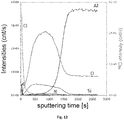
- the SIMS depth profiling exhibits a concentration of chlorine that is rapidly decreasing as a function of the sputtering time ( figure 12 ).
- the intensity of Cl is starting a decade less, around 3.5e4 cnts/s.
- the amount of C is moreover comparable but the N concentration is slightly increasing inside the film ( ⁇ 750s sputtering time). This confirms the low level of NH 4 Cl contamination included in a thick volume of SiO 2 .
- the higher concentration of chlorine close to the surface of the film hint the slow dissociative chemisorption of water that induces the desorption of HCI. This recombination clearly affects the growth mechanism of silicon dioxide.
- the conductivity of the dense SiO 2 film obtained through the pure ALD is in the range of a 50nm thermal oxide (10 -7 - 10 -8 S/cm).
- the conductivity measured for the dense SiO 2 is anyway ⁇ 10 3 higher than the standard oxide produced with a constant flow of NH 3 ( ⁇ 10 -11 S/cm).
- the thick porous SiO 2 exhibits a low conductivity of 200 ⁇ S/cm. This could be attributed to the amount of -OH groups associated to a specific area that is higher than in a compact film.
- this porous SiO 2 layer could be used as transparent backside coating or as a first passivation layer. No additional transparent, such as Al 2 O 3 for instance, layer has been added in order to demonstrate the inherent properties of the as-developed film.
- the versatility of the ALD process allows the production of a tunable low- ⁇ layer at room temperature. This could be in line with many temperature-sensitive hybrid applications.
- Hydrophilic or superhydrophilic surfaces can be created by tuning the roughness at the nanoscale or the porosity of a film. This is peculiar in various applications such as antibacterium, heat transfer or biomedical applications. Hence, the wettability of the film has been analysed by water contact angle (WCA) and results are shown in figure 15 . Compared to the untreated silicon surface ( figure 15a ), the porous SiO 2 layer demonstrates a remarkable super-hydrophilic behaviour ( ⁇ 5°). According to the XPS analyses, this could be attributed to the high concentration of oxygen in the porous film which presents a significant aspect ratio.
- the interest of hydrophilic behaviour commonly based on TiO 2 for instance [ Huang T., et al., Surf. Coat. Techno., 2012, 213, 126-132 ) could be transposed to a standalone porous SiO 2 layer.
- ARC anti-reflective coatings
- the main advantage to add an anti-reflective layer on optically active device (i.e. solar cells) is to improve the efficiency [ Mazur M., et al., Opto-Electron. Rev., 2013, 21, 233-238 ].
- the reflectivity has been checked by ellipsometry with two grazing angles, i.e. 75 and 81 degrees (see figure 16 ).
- the specular reflection has been surrounded by a spatial reflectance analysis in order to validate the anisotropy of the film and the results are shown in figure 17 .
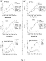
- a remarkable decrease of the reflectance percentage is observed in both cases of coating glass or silicon.
- the signal is constantly decreasing as a function of the thickness of the film but only extreme results are shown here for clarity.
- the reflectance reduction is about ⁇ 10-15% for Si
- the scaling down for glass is maintained in the region of ⁇ 50% especially for high reflection at grazing angle for glass.
- the combination of the maintain of substantial reflection percentage at various incident angles with less than 200nm coating gives a good opportunity to use this room temperature process in a wide range of transparent applications.
- the possibility to tailor this process through the versatility of ALD may of interest to avoid multifunctional coatings.
Landscapes
- Chemical & Material Sciences (AREA)
- General Chemical & Material Sciences (AREA)
- Chemical Kinetics & Catalysis (AREA)
- Engineering & Computer Science (AREA)
- Materials Engineering (AREA)
- Mechanical Engineering (AREA)
- Metallurgy (AREA)
- Organic Chemistry (AREA)
- Inorganic Chemistry (AREA)
- Chemical Vapour Deposition (AREA)
- Formation Of Insulating Films (AREA)
Description
- The invention is directed to the field of deposition of silicon oxide on a substrate, notably an inorganic material.
- Silicon dioxide (SiO2) and more generally oxide ultrathin films have been widely described as good components in modern nanotechnologies like dielectric material in silicon microelectronic devices [Frosch C.J., et al., J. Electrochem. Soc., 1957, 104, 547-552], anticorrosion films [Olsson C.O.A., et al., Electrochim. Acta, 2003, 48, 1093-1104] or non-exhaustive applications of nanoscale films in catalysis. The environmentally and human safe state of SiO2 induces its wide use in protective layers for antisticking, antifogging, self-cleaning or water repellency. For instance, various techniques such as chemical vapor deposition [Ragesh P., et al., J. Mater. Chem. A., 2014, 2, 14773-14797], lithographic patterning [Park H.K., et al., J. Mat. Chem., 2012, 22, 14035-14041], electrochemical deposition [Gao Y., et al., ACS App. Mat.&Inter., 2014, 6, 2219-2223] or sol-gel [Xu B., et al., Surf. Coat. Techno., 2010, 204, 1556-1561] are investigated to elaborate superhydrophobic SiO2 through the tuning of surface roughness or energy. SiO2 is consistently known for protective or gate insulator coatings [Klaus J.W., et al., Science, 1997, 278, 1934-1936], interfacing high-κ materials [Wang X., et al., Appl. Phys. Lett., 2010, 97, 062901-062903] or surface passivation [Dingemans G., et al., J. Appl. Phys., 2011, 110, 09371-093716].
- The increasing demand for transparent active materials in the nanoscale justify the need of a deposition technique compatible with sensitive pre-deposited underlying layer, flexible plastic devices or high aspect ratio substrates. Therefore, Atomic Layer Deposition (ALD) is considered as one of the most suitable technique for its performances in terms of sub-nanometer thickness control and penetration coating into deep trenches or mesoporous structures.
- Although the improvement SiO2 coatings obtained at high temperatures engaged a lot of efforts towards ALD parameters or precursors, the question of the deposition at room temperature nevertheless emerged. George et al. described many times this atomic layer-controlled growth using SiCl4 and H2O [Du Y., et al., Thin Solid Films, 2005, 491, 43-53]. They demonstrated that a catalysed reaction using Lewis bases such as pyridine or ammonia avoid large precursor fluxes and can only occur close to room temperature. Nevertheless, in these reported studies, pyridine or ammonia was never really considered as a "precursor". The proposed mechanism that considered the hydrogen bonding between the Lewis base and either the SiOH* surface species or the H2O reactant was studied by considering the global residual pressure of a continuous flow of catalyst. Moreover, since a pollution of the film through the inclusion of contaminants arise through the secondary reaction of pyridine or ammonia with the byproduct HCl, a sequential approach could enhance the quality of the film and the understanding of the role of the catalyst.
- Silicium oxide (SiO2) films made at room temperature have been described as feasible by the exposition of two reactants (A and B) through a sequential exposition (ABAB...). Many well-known precursors require high deposition temperatures, plasma or highly reactive co-reactant such as ozone gas [Kim H.-U., et al., J. Electrochem. Soc., 2000, 147, 1473-1476]. Nearly correlated to CVD-based processes and despite a low enthalpy of reaction, silicium tetrachloride (SiCl4) usually reacts with water (oxidant specie) at high temperatures (>325°C) [Klaus J.W., et al., Science, 1997, 278, 1934-1936]. A comparison of thermal ALD and room temperature processes reveal a higher growth rate/ALD cycle in favour of room temperature reactions (∼2Å/cycle).
- George et al. described the mechanism that spontaneously takes place through a catalysed binary reactions using pyridine or ammonia as a Lewis base agent [Klaus J.W., et al., Surf. Rev. Lett., 1999, 6, 435-448]. The hydrogen bonding between the Lewis base and SiOH* (surface specie) or H2O allows the reaction to be performed at room temperature. Compared to high temperature processes that use large exposures (>103 Torr.s), SiO2 room temperature ALD is permitted trough the strong nucleophile attack of the oxygen from (i) SiOH* on SiCl4 and (ii) from H2O on SiCl* [Du Y., et al., Thin Solid Films, 2005, 491, 43-53]. Nevertheless, according to our knowledge, no specific data have been described regarding the variation of the chemical composition and the morphology of such films. Based on the catalytic effect of NH3, it can be clearly deduced that a constant flow of NH3 statistically ensures a maximized reaction of -O on all -O-Si-(Cl)n available sites. Nonetheless, the perfect delimitation of the exposure windows at room temperature could be enhanced by working in a non-conventional high vacuum state (<10-6 Torr). As it may not be the case for standard ALD reactors like in our case, we tried to understand and control the mechanism of contaminants inclusion in this regime. Thus, the state-of-the-art production of SiO2 at room temperature (∼25°C) using a constant flow of NH3 has been compared to pulse NH3-catalysed RT-ALD.
- Inspired by the reactivity of chlorinated precursors described in the literature [Damyanov D., et al., J. Non-Cryst. Solids, 1988, 105, 107-113], the amount of contamination could be cautiously explained by the functionality x of the adsorbed 137 specie at the surface explained hereafter:
x(≡Si-OH) + SiCl4 → (≡Si-O)xSiCl4-x + xHCl
- x = 1 : monofunctional
- x = 2 : bifunctional
- X = 3 : trifunctional
- The injected precursor SiCl4 reacts with the surface hydroxyl species. The competition between the single bond case (x = 1) and multiple bonds (1 < x ≤ 3) is directly linked to the stagnancy of precursors in the ALD regime. As far as the concentration of hydroxyl groups on the surface is increased, the saturation of H2O will directly enhance the formation of HCl. Concurrently with the constant flow of ammonia, the ∼2.2 Si/N ratio measured by XPS in the bulk of the film also indicates that strong nitrogen contamination exceed acceptable limits, especially through the inclusion of NH4Cl salts. As indicated by George et al. [Klaus J.W., et al., Surf. Sci., 2000, 447, 81-90], this salt is formed as a result of the NH3 catalyst complexing with the HCI reaction product. Due to the vapour pressure of NH4Cl salt (i.e. 4.10-5 Torr), some quantity of salts are remained inside the film. In that context, it is noteworthy that compared to an inert gas, using NH3 in a carrier gas mode may not contribute to a pure ALD process performed at room temperature.
- European patent application published
EP 1 925 691 A1 - The invention has for technical problem to provide porous silicon oxide layers with a significant decrease of the amount of contaminants, such as chlorine, included in the film.
- The invention is directed to a process of atomic layer deposition for the coating of silicon oxide on a substrate, notably an inorganic material, performed at room temperature, involving at least three precursors, said at least three precursors being silicon tetrachloride, water and one Lewis base agent, said one Lewis base agent being preferentially ammonia. Said process comprises the steps of (a) exposing on said substrate during an exposure time said one Lewis base agent, (b) exposing on said substrate during an exposure time said silicon tetrachloride, and (c) exposing on said substrate during an exposure time said water. Said process is remarkable in that at least one step of purge with nitrogen gas is performed after each of the steps (a), (b) and (c) during a purge time.
- In one embodiment, said at least one step of purge with nitrogen gas presents a ratio of nitrogen gas flow/total pressure which is inferior to 5 Torr, 4 Torr, 3 Torr, 2 Torr or 1 Torr, preferentially inferior to 2 Torr.
- In one embodiment, said exposure time of the precursors is comprised between 50 milliseconds and 200 seconds.
- In one embodiment, the exposure time of the silicon tetrachloride is comprised between 50 milliseconds and 200 milliseconds, preferentially comprised between 80 milliseconds and 120 milliseconds, more preferentially of 100 milliseconds; and the exposure time of said Lewis base agent and of said water is comprised between 1 second and 3 seconds, preferentially comprised between 1.8 seconds and 2.2 seconds, more preferentially of 2.0 seconds.
- In one embodiment, said exposure time of the precursors is comprised between 50 seconds and 200 seconds, preferentially comprised between 70 seconds and 99 seconds, more preferentially of 71, 72, 73, 74, 75, 76, 77, 78, 79, 80, 81, 82, 83, 84, 85, 86, 87, 88, 89, 90, 91, 92, 93, 94, 95, 96, 97 or 98 seconds, even more preferentially of 90 seconds.
- In one embodiment, said purge time with nitrogen gas is comprised between 1 second and 20 seconds, preferentially comprised between 5 seconds and 15 seconds, more preferentially of 10 seconds.
- In one embodiment, the purge time with nitrogen gas after step (a) is comprised between 100 seconds and 240 seconds, preferentially comprised between 160 seconds and 200 seconds, more preferentially of 180 seconds; the purge time with nitrogen gas after step (b) is comprised between 10 seconds and 100 seconds, preferentially comprised between 40 seconds and 80 seconds, more preferentially of 60 seconds; and the purge time with nitrogen gas after step (c) is comprised between 200 seconds and 360 seconds, preferentially comprised between 280 seconds and 320 seconds, more preferentially of 300 seconds.
- In one embodiment, said steps (a), (b) and (c) with concomitant purge steps are repeated between 50 and 5000 times, preferentially between 500 and 2500 times.
- In one embodiment, said inorganic material is composed of silicon, silicon oxide, titanium, titanium oxide, aluminium, aluminium oxide, zinc, zinc oxide or any combinations thereof, or any other, preferentially silicon.
- In one embodiment, said silicon materials are cleaned in accordance with RCA procedure before the steps of exposing.
- In one embodiment, said process is carried out in a reactor which is equipped with a residual gas analyser adapted for determining said exposure time and said purge time.
- In one embodiment, said reactor is further equipped with a quartz crystal microbalance adapted for the gravimetric monitoring of the film growth and/or a mass spectrometer adapted for monitoring the gas composition.
- The invention is further directed to a film of silicon oxide obtained by the process as described in the first part of the present invention. Said film of silicon oxide is remarkable in that it comprises a level of chlorine contaminant which is inferior to 5%, 4%, 3%, 2% or 1% of the total mass of said film of silicon oxide, preferably inferior to 3% of the total mass of said film of silicon oxide.
- In one embodiment, said film of silicon oxide comprises pores, said pores being preferentially micropores, mesopores or nanopores (i.e. < 50 nm).
- In one embodiment, said film of silicon oxide comprises superhydrophilic properties, anti-reflective properties and/or insulating properties.
- The invention is particularly interesting in that the correlation of the high aspect ratio and the oxygen concentration exhibits a super-hydrophilic behaviour. The silicon oxide thin films of the present invention further manifest a weak conductivity. The optimized room temperature ALD (RT-ALD) process can further be applied on a wide range of substrates that need to be 3D-coated with a low-κ porous silicon oxide layer or any 3D temperature-sensitive materials requiring super-hydrophilic treatments.
-
-
Figure 1 : ALD room temperature growth of SiO2 under NH3 catalytic regime. -
Figure 2 : Saturation curves of SiCl4, H2O and NH3 along the SiO2 thin film growth. The growth kinetic is shown for 5 cycles sequential exposure of the surface. -
Figure 3 : Growth kinetics of pure ALD SiO2 growth with sequential exposure of the surface to 90s of SiCl4, 90s of NH3 and 90s of H2O. A typical zoom of the in situ monitoring of 500 loops deposition shown in panel (a) corresponds to a growth rate of 0.02 µg/cm2. The panel (b) represents a zoom of the 60% advanced deposition. Lower panels represent the programmed exposures of SiCl4, NH3 and H2O, respectively. -
Figure 4 : Growth kinetics of SiO2 for sequential exposure of the surface to 90s of SiCl4, and 90s of H2O, indicating a growth rate of 0.6 µg/cm3 per cycle. Panel (a) shows a typical zoom on 10 cycles of the total 2000 cycles deposited film. Panel (b) corresponds to the view of 2 cycles deposition. Lower panel represent the programmed exposure of H2O, SiCl4 and NH3, respectively. -
Figure 5 : In-situ RGA mass spectrometric monitoring of successive 90s H2O pulses alternated with 300s N2 purge. The panel corresponds to the measured intensity of H2O (m/z = 18 uam) (uam = unified atomic mass). -
Figure 6 : XPS spectra of SiO2 thin film obtained with a sequential 90s exposure of SiCl4, NH3 and H2O precursors. Upper panel corresponds to the signal of the raw film and lower panel to the film after surface cleaning. -
Figure 7 : SIMS depth profile of pure ALD SiO2 film obtained with 90s pulse of SiCl4, NH3 and H2O precursors and extended N2 purges, respectively 60, 180 and 300s. Fast and slow sputtering rate are shown respectively in panels (a) and (b). -
Figure 8 : SEM images of the 500 cycles processed pure ALD SiO2 film at different magnifications: (a) top and (b) 45° tilted view of the entire oxide film; (c, d) FIB cross-section images reveal a dense state of the SiO2 film with an inhomogeneous crystallisation due to the unescapable inclusion of contaminants and the low growth rate of 0.5 Å/cycle. -
Figure 9 : Growth kinetics of porous SiO2 growth with sequential exposure of the surface to 100ms of SiCl4, 2s of NH3 and 2s of H2O. The in situ monitoring of 300 loops deposition corresponds to a growth rate of 1.5 µg/cm2 per cycle. The insert represents a zoom of 10 cycles process. -
Figure 10 : XPS spectra of SiO2 thin film obtained with a sequential exposure of SiCl4, NH3 and H2O precursors. SiO2 film deposited on (a) Si wafer, (b, c) TiO2/Si (80 nm) before and after surface cleaning respectively. -
Figure 11 : XPS quantification of the suitable element of the SiO2 thin film obtained with an optimized ALD regime on a TiO2/Si substrate (above) and a Si substrate (below). -
Figure 12 : SIMS depth profile of porous SiO2 film obtained with 100ms pulse of SiCl4, 2s of NH3, and H2O precursors. -
Figure 13 : SEM images of the -260 nm thick ALD SiO2 (300 loops) film at different magnifications: (a) top and (b) 45° tilted view of the entire oxide film; (c, d) FIB cross-section confirms the porous state of the film. -
Figure 14 : Conductivity measurements of the porous SiO2 film compared to a standard thermal oxide made by rapid thermal CVD (100 nm). -
Figure 15 : Water contact angle images of (a) Si wafer, (b) porous SiO2 and (c) top view of the substrate after depositing the water drop. -
Figure 16 : Schematic of the reflection ellipsometric measurements. The variable maximum angle θm is set at two different effective grazing angles θe = 75 and 81°. Data were acquired in the full wavelength range 350-1000 nm. The spatial reflectance has been measured by counterclockwise rotating the sample as a function of the planar angle τR. Z-axis is fixed at zero to maximise the reflected intensity. -
Figure 17 : Reflection results obtained by using the ellipsometer at two different grazing angles (respectively 75° and 81°). The reflectance percentage has been measured for SiO2 deposited on glass (a ,d) and silicon (b, e). The spatial reflection (c, f) confirms the homogeneity of the film with a limited variation of the signal as a function of the τR angle. -
Figure 18 : SEM images of various thickness ALD SiO2 (100-300 loops) deposited on anodic aluminium oxide (AAO) membranes. - ALD processes were performed in a TFS200-Beneq reactor in the planar configuration at a base pressure of 0.3 mbar. SiO2 thin films were deposited on silicon substrates preliminary cleaned with a standard RCA procedure. The deposition reactor is equipped with a quartz crystal microbalance, QCM, (Neyco) for the gravimetric monitoring of the film growth. The QCM was fixed at the central part of the substrate holder. A quadrupole mass spectrometer, Vision-2000C, MKS-instrument, was mounted at the outlet of the deposition reactor to monitor the exhaust gas composition. SiO2 thin films were obtained at room temperature using silicon tetrachloride (SiCl4) and water (H2O) as precursors. Vaporized precursors were transferred to the ALD reaction chamber with nitrogen (N2) carrier gas. SiCl4 precursor was purchased from Sigma Aldrich and used as received. Both canisters containing the precursors were maintained at 19 °C during deposition.
- Morphology and thickness of the obtained samples were obtained on FEI Heliosnanolab 650 Focused Ion Beam Secondary Electron Microscope (FIB-SEM). The elemental composition depth profile was assessed by Dynamic Secondary Ion Mass Spectrometry (D-SIMS) (Cameca IMSLAM) while the quantification was performed by X-ray photoelectron spectroscopy (XPS) (Thermo VG Scientific, MicroLab 350) using an Al X-Ray source. The thickness, refractive index and reflectance were determined using the UVISEL spectroscopic phase modulated ellipsometer, Horiba scientific using a Cauchy function for analysis. The hydrophobic behaviors of the deposited films were determined by water contact angle (WCA) measurements using drops of water. Additionally, the dielectric properties of the films were determined using a Novolab broadband dielectric spectrometer.
- As described by Klaus et al. [Klaus J.W., et al., Surf. Rev. Lett., 1999, 6, 435-448], the process described here above confirms that NH3 gas molecule acts as a catalyst for the deposition of SiO2 at room temperature (between 20°c and 26°C). Nevertheless, a significant contamination of the surface is coming from the excessive dose of ammonia. The contamination depicted here confirms the already described importance of adjusting the quantity of NH3 to limit the reaction between HCl and NH3. Thus, we considered that tuning the pulses of NH3 like the other precursors could minimize unfavourable reactions at room temperature.
- Based on the same chemistry used in the previous part, each chemical involved in the following process has been considered as a precursor. This means that an adequate separation of each pulsed chemical has been guaranteed. The purge of the reactor has been optimized using the appropriate ratio of carrier gas flow / total pressure (<2 Torr). Any overlapping between each precursor pulse has been prevented by checking the injection with the integrated Residual Gas Analyser (RGA).
-
Figure 1 depicts the growing of a SiO2 monolayer. Through the injection of NH3 (under catalytic regime), the O-H bond becomes weaker, -Si can easily react with -O at the surface to form -O-Si-(Cl)3 or -O-Si(Cl)2-O-ligands at the surface. -O coming from water injection directly react with - Si to finally form a SiO2 monolayer. -
Figure 2 shows the ALD saturation curves at room temperature for SiCl4, H2O and NH3 precursors. In our reactor configuration, primary experiments demonstrated that the saturation time for all precursors occurred between 60s and 100s. The timing sequence of the experiment starts with a variable SiCl4 exposure followed by a 90s N2 purge. Next, a 90s NH3 exposure was followed by a 180s N2 purge. Lastly, the cycle was ended by a 90s H2O pulse and a longer N2 purge of 300s to ensure a complete release of the subsequent unadsorbed water. This value of 300s has been validated by the RGA. -
Figure 2a shows the mass gain versus exposure time for various SiCl4 pulses switched from 500ms to 150s. The profile presents a saturation over t = 90s. A subsequent SiCl4 exposure, not shown here for clarity, produce a smaller mass gain even no gain. This can be observed through the saturation of the curve over 90s. The total weight gain resulting from 5 cycles is about 0.13 µg/cm2. -
Figure 2b shows the mass gain versus exposure time forvarious H 20 pulses switched from 500ms to 150s. Starting with the previously obtained value for SiCl4 (i.e. 90s), the cycle is kept identical and a various H2O exposure time is applied. A maximum weight gain of 0.18 µg/cm2 is reached for 90s and the saturation regime is reached over this value. -
Figure 2b shows the mass gain versus exposure time for various NH3 pulses switched from 500ms to 150s. SiCl4 and H2O are both maintained at 90s, a maximum of 0.17 µg/cm2 gain of mass is observed over 90s NH3 exposure. - The trends observed in
figure 2 were used to investigate the growth of a SiO2 film in a pure ALD regime at room temperature. SiCl4, NH3 and H2O exposure times were fixed at 90s and extended purges were applied after NH3 and H2O pulses, respectively 180s and 300s. A purge for SiCl4 lasting 60s was applied. - Those finely tuned fluxes of precursors allow the surface reactions to perform smoothly and in particular, it allows a significant decrease of the amount of contaminants, such as chlorine, but also nitrogen, carbon and any others, which might be included in the silicon oxide thin film.
- As shown in
figure 3 , the 0.02 µg/cm2 per cycle weight gain is 30 times lower than the process done with a constant flow of NH3 (which is depicted infigure 4 ). Nevertheless, the injection of NH3 and H2O precursors noteworthy contributes to a certain gain of mass (seefigure 3b ) and a growth rate of 0.5 Å/cycle is obtained for 500 cycles deposition (i.e. a higher mass is depicted for H2O). This confirms that the interaction of H2O molecules with active complex of the surface ends through the efficient replacement of chlorine by hydroxyl groups (as shown infigure 1 ). - In our case, the appropriate purging time of water has been determined by using a systematic variation using the RGA (H2O: m/z = 18 uam). The trend shown in
figure 5 reveals a 300s purge time needed to decrease down to the base line. - The XPS elemental analysis (
figure 6 ) still shows the presence of chlorine, nitrogen and Carbon in addition of silicon and oxygen. The amount of contaminants is nonetheless substantially decreased. First, the Si/Cl ratio is going from ∼4 (surface) to ∼8.7 in the bulk of the film. Secondly, compared to the films obtained with a constant flow of ammonia, the Si/Cl ratio is significantly improved (8.7 versus 3). Moreover, the Si/N ratio is heightened from 1.1 to 3.8 (resp. 2.2 to 5.9 inside the film). This indicates a limited reaction between hydrogen chloride with ammonia to form ammonium chloride. High resolution fitting of N1s reveals a single binding energy at 401.1± 0.3 eV corresponding to NH3 +. This confirms the formation of ammonium chloride salt. The small amount of detected Al is attributed to the alumina sub-layer (i.e. SiO2/Al2O3/Si). - The SIMS depth profile of the SiO2 film is shown in
figure 7 . The intensity of chlorine is decreasing ∼30 times faster than the process done with the constant NH3 flow. In fact, less than 100s sputtering are needed to decrease the intensity below 1e5 cnts/s compared to ∼2800s for the NH3 constant flow process. Additionally, the intensity of nitrogen seems to be in the same range of 10 to 100 cnts/s. Related to XPS results, this corroborates the formation of NH4Cl salt. The intensity of Si is nonetheless higher than Al, confirming the coating process of SiO2 on Al2O3. Based on XPS and SIMS results, it can be assumed that this room-temperature process is optimized in terms of surface exposure. Nevertheless, residual traces of hydrochloric acid still react with ammonia due to the difficulties to purge water or ammonia at room temperature. Tittle by-products quantities, such as ammonium chloride, are consequently integrated into the film. -
Figure 8 shows the top-view and cross-section SEM images of the SiO2 film. We observe a porous layer with grains size up to 200nm. A significant roughness is observed in the 45° tilted view (figure 8c ). Additionally, cross-section analyses evidence an inhomogeneous crystallisation into the film (figure 8d ). A thickness of ∼30nm±5nm is measured through the cross-section, also confirming the ∼25nm value deduced from the SIMS pulverisation speed of silicon oxide. This lead to a low growth rate of ∼0.5 Å/cycle related to the lower weight gain observed with the QCM (i.e. 30x lower than the SiO2 film processed under a constant flow of ammonia). Nevertheless, the type of crystallisation reveals that the process is not corresponding to a pure ALD growth mode as expected [Ritala M., et al., Chem. Vap. Depos., 1999, 5, 7-9]. This peculiar non-homogeneous growth at room temperature suggests that the surface reaction is in competition with the integration of contaminants. The self-limiting process actually promote the deposition of species onto the substrate and onto the deposits (e.g. islands, ...) with equal probability, if we consider that no particles can be produced in a CVD mode, then the inclusion of contaminants at a sub-atomic growth rate (i.e. < 1 Å/cycle) could explain the morphology of the obtained film. Moreover, the high amount of hydrogen bonded terminal -OH groups could affect the dehydroxylation-rehydroxylation equilibrium leading to a higher quantity of HCl produced in the case of trifunctional bonds. Nevertheless, the oxide layer display a significant density in volume and the amount of inhomogeneous crystallites is limited. This is in line with the sub-atomic growth rate mechanism surrounded by a limited contamination. The tailoring of the ALD parameters in this RT-SiO2 growth process manifests a substantial adaptability in terms of morphology and chemical composition. These results let suggest that a tuning of the growth parameters could influence the crystallisation that occurs. Hence, different type of SiO2 layers could be processed at room temperature. - Low contaminants SiO2 can be produced by adjusting the surface exposure of SiCl4, NH3 and H2O precursors. Furthermore, the impact of a limited exposition to the composition and the morphology of the film has been carried out. Hence, the process has been tuned to maintain the low level of contaminants in an ALD non-saturation regime. The precursor exposure has been decreased to a minimum value for SiCl4 (i.e. 100 ms) in agreement with a low contamination strategy. Then, according to RGA results, the exposure time of NH3 and H2O has been fixed to 2s for both with a purge of 10s using 300 sccm of nitrogen.
- As shown in
figure 9 , a growth rate of 1.54 µg/cm2 per cycle is obtained. Compared to the previous processes, the exposure reaction used here generates a ∼50 times higher weight gain. In order to screen any physicochemical influence from the substrate, silicon oxide films were performed by intercalating a pre-characterized barrier layer. Hence SiO2 growth has been investigated on two different sub-layers, i.e. TiO2 deposited by ALD and Si bulk. -
Figure 10 shows the XPS experiment results. As expected, Cl, C, N elements are detected for both samples. In the case of the oxide deposited on TiO2, the detection of Ti-2p before cleaning confirms the low thickness of the film. However the percentage of chlorine is clearly maintained below the limit of 3% obtained for the previous process with extended exposures likewise N and C (figure 11 ). Nevertheless, chlorine concentration is increasing as far as the titanium oxide layer is reached through the sputtering. Since chlorine is inherent to the TiO2 ALD elaboration, the chlorine concentration is effectively lower in the film as indicated by the deposit on Si directly (figure 11 - SiO2/Si). In order to screen the composition and the porous structure of the film, thicker SiO2 (2500 loops) has been processed on a layer without chlorine contamination, i.e. Al2O3 on Si (50 nm). - The SIMS depth profiling exhibits a concentration of chlorine that is rapidly decreasing as a function of the sputtering time (
figure 12 ). Compared to the previous process, the intensity of Cl is starting a decade less, around 3.5e4 cnts/s. The amount of C is moreover comparable but the N concentration is slightly increasing inside the film (∼750s sputtering time). This confirms the low level of NH4Cl contamination included in a thick volume of SiO2. Additionally, the higher concentration of chlorine close to the surface of the film hint the slow dissociative chemisorption of water that induces the desorption of HCI. This recombination clearly affects the growth mechanism of silicon dioxide. - As shown in
figure 13 , SEM analyses establish the porous state of the oxide film. Except the presence of 200 nm to 500 nm diameter aggregates on the surface of the layer, the top and tilted views (resp.figure 13a and 13b ) reveals directly a SiO2 spongy nature. The applied FIB cross-section (figures 13c and 13d ) reveals also the presence of 20-50nm cavities related to a porous film. Compared to the film obtained through the pure ALD process, it is worth notable that the mechanisms involved in this growth process generate alternatively hollow volume on behalf of the migration into surface crystallites. As explained in the ALD random deposition approach [Puurunen R.L., Chem. Vap. Dep., 2004, 10, 159-170], if the growth per cycle is not constant, the surface roughness should increase faster at the beginning of growth and slowly thereafter. This implies naturally that a smaller number of ALD reaction cycles are needed to fit a conformal deposition in a close-packed array as far as the growth rate is adjacent to an atomic monolayer. - By considering the growth rate of ∼0.11 Å/cycle obtained in this process, this could explain why the SiO2 film is much closed as the one processed under the pure ALD approach. Nevertheless, its spongy state may be related to surface diffusion that are (i) on one hand limited due to the room temperature reaction and (ii) on the other hand widely promote during extended purges during the pure ALD process. In that case, residual water or byproducts (NH4Cl, HCl) are considered as surface fractions where the supplementary amount of injected precursor will be adsorbed, leading to a non-uniform film. This peculiar structure is nonetheless attractive for some applications that need to be processed at room temperature.
- The performances have been checked for both SiO2 dense and porous film.
- We investigated the dielectric characterizations on the SiO2 films obtained in this work and we compared it to a standard thermal oxide (RTO; 1100°C; 1h). As shown in
figure 14 , the conductivity of the dense SiO2 film obtained through the pure ALD is in the range of a 50nm thermal oxide (10-7 - 10-8 S/cm). The conductivity measured for the dense SiO2 is anyway ∼103 higher than the standard oxide produced with a constant flow of NH3 (∼10-11 S/cm). Furthermore, the thick porous SiO2 exhibits a low conductivity of 200 µS/cm. This could be attributed to the amount of -OH groups associated to a specific area that is higher than in a compact film. - Despite its low-κ state, this porous SiO2 layer could be used as transparent backside coating or as a first passivation layer. No additional transparent, such as Al2O3 for instance, layer has been added in order to demonstrate the inherent properties of the as-developed film.
- The versatility of the ALD process allows the production of a tunable low-κ layer at room temperature. This could be in line with many temperature-sensitive hybrid applications.
- Hydrophilic or superhydrophilic surfaces can be created by tuning the roughness at the nanoscale or the porosity of a film. This is peculiar in various applications such as antibacterium, heat transfer or biomedical applications. Hence, the wettability of the film has been analysed by water contact angle (WCA) and results are shown in
figure 15 . Compared to the untreated silicon surface (figure 15a ), the porous SiO2 layer demonstrates a remarkable super-hydrophilic behaviour (<5°). According to the XPS analyses, this could be attributed to the high concentration of oxygen in the porous film which presents a significant aspect ratio. The interest of hydrophilic behaviour commonly based on TiO2 for instance [Huang T., et al., Surf. Coat. Techno., 2012, 213, 126-132) could be transposed to a standalone porous SiO2 layer. - One of the other aspects of porous layer applications is the possibility to create anti-reflective coatings (ARC). The main advantage to add an anti-reflective layer on optically active device (i.e. solar cells) is to improve the efficiency [Mazur M., et al., Opto-Electron. Rev., 2013, 21, 233-238]. The reflectivity has been checked by ellipsometry with two grazing angles, i.e. 75 and 81 degrees (see
figure 16 ). The specular reflection has been surrounded by a spatial reflectance analysis in order to validate the anisotropy of the film and the results are shown infigure 17 . A remarkable decrease of the reflectance percentage is observed in both cases of coating glass or silicon. The signal is constantly decreasing as a function of the thickness of the film but only extreme results are shown here for clarity. As the reflectance reduction is about ∼10-15% for Si, the scaling down for glass is maintained in the region of ∼50% especially for high reflection at grazing angle for glass. The combination of the maintain of substantial reflection percentage at various incident angles with less than 200nm coating gives a good opportunity to use this room temperature process in a wide range of transparent applications. Furthermore, the possibility to tailor this process through the versatility of ALD may of interest to avoid multifunctional coatings. - The evident interest of this porous SiO2 layer has been applied to a 3D material. Various thickness of SiO2 has been deposited on an anodic aluminium oxide (AAO) membrane and results are shown in
figure 18 . It clearly appears that the porosity obtained on planar substrates is transposed on 3D surfaces. This let suggest many applications that need hydrophilicity or low contaminants layer with a high precision on thickness deposited.
Claims (12)
- Process of atomic layer deposition for the coating of silicon oxide on a substrate, notably on an inorganic material, performed at room temperature, involving at least three precursors, said at least three precursors being silicon tetrachloride, water and one Lewis base agent, said one Lewis base agent being preferentially ammonia, comprising the steps ofa. exposing on said substrate during an exposure time said one Lewis base agent,b. exposing on said substrate during an exposure time said silicon tetrachloride, andc. exposing on said substrate during an exposure time said water,wherein at least one step of purge with nitrogen gas is performed after each of the steps (b) and (c) during a purge time,
characterized in that
at least one step of purge with nitrogen gas is also performed after step (a) during said purge time. - Process according to claim 1, characterized in that said at least one step of purge with nitrogen gas presents a ratio of nitrogen gas flow/total pressure which is inferior to 5 Torr, 4 Torr, 3 Torr, 2 Torr or 1 Torr, preferentially inferior to 2 Torr.
- Process according to any one of claims 1-2, characterized in that said exposure time of the precursors is comprised between 50 milliseconds and 200 seconds.
- Process according to any one of claims 1-3, characterized in thata. the exposure time of the silicon tetrachloride is comprised between 50 milliseconds and 200 milliseconds, preferentially comprised between 80 milliseconds and 120 milliseconds, more preferentially of 100 milliseconds; andb. the exposure time of said Lewis base agent and of said water is comprised between 1 second and 3 seconds, preferentially comprised between 1.8 seconds and 2.2 seconds, more preferentially of 2.0 seconds.
- Process according to any one of claims 1-3, characterized in that said exposure time of the precursors is comprised between 50 seconds and 200 seconds, preferentially comprised between 70 seconds and 99 seconds, more preferentially of 71, 72, 73, 74, 75, 76, 77, 78, 79, 80, 81, 82, 83, 84, 85, 86, 87, 88, 89, 90, 91, 92, 93, 94, 95, 96, 97 or 98 seconds, even more preferentially of 90 seconds.
- Process according to any one of claims 1-4, characterized in that said purge time with nitrogen gas is comprised between 1 second and 20 seconds, preferentially comprised between 5 seconds and 15 seconds, more preferentially of 10 seconds.
- Process according to any one of claims 1-3 or 5, characterized in thata. the purge time with nitrogen gas after step (a) is comprised between 100 seconds and 240 seconds, preferentially comprised between 160 seconds and 200 seconds, more preferentially of 180 seconds;b. the purge time with nitrogen gas after step (b) is comprised between 10 seconds and 100 seconds, preferentially comprised between 40 seconds and 80 seconds, more preferentially of 60 seconds; andc. the purge time with nitrogen gas after step (c) is comprised between 200 seconds and 360 seconds, preferentially comprised between 280 seconds and 320 seconds, more preferentially of 300 seconds.
- Process according to any one of claims 1-7, characterized in that said steps (a), (b) and (c) with concomitant purge steps are repeated between 50 and 5000 times, preferentially between 500 and 2500 times.
- Process according to any one of claims 1-8, characterized in that said inorganic material is composed of silicon, silicon oxide, titanium, titanium oxide, aluminium, aluminium oxide, zinc, zinc oxide or any combinations thereof, or any other, preferentially silicon.
- Process according to claim 9, characterized in that said silicon materials are cleaned in accordance with RCA procedure before the steps of exposing.
- Process according to any one of claims 1-10, characterized in that said process is carried out in a reactor which is equipped with a residual gas analyser adapted for determining said exposure time and said purge time.
- Process according to claim 11, characterized in that said reactor is further equipped with a quartz crystal microbalance adapted for the gravimetric monitoring of the film growth and/or a mass spectrometer adapted for monitoring the gas composition.
Applications Claiming Priority (2)
| Application Number | Priority Date | Filing Date | Title |
|---|---|---|---|
| LU92795A LU92795B1 (en) | 2015-08-10 | 2015-08-10 | SIO2 thin film produced by atomic layer deposition at room temperature |
| PCT/EP2016/068899 WO2017025516A1 (en) | 2015-08-10 | 2016-08-08 | Sio2 thin film produced by atomic layer deposition at room temperature |
Publications (2)
| Publication Number | Publication Date |
|---|---|
| EP3359706A1 EP3359706A1 (en) | 2018-08-15 |
| EP3359706B1 true EP3359706B1 (en) | 2019-03-20 |
Family
ID=53879744
Family Applications (1)
| Application Number | Title | Priority Date | Filing Date |
|---|---|---|---|
| EP16751563.4A Not-in-force EP3359706B1 (en) | 2015-08-10 | 2016-08-08 | Sio2 thin film produced by atomic layer deposition at room temperature |
Country Status (5)
| Country | Link |
|---|---|
| US (2) | US11041238B2 (en) |
| EP (1) | EP3359706B1 (en) |
| JP (1) | JP7011325B2 (en) |
| LU (1) | LU92795B1 (en) |
| WO (1) | WO2017025516A1 (en) |
Cited By (1)
| Publication number | Priority date | Publication date | Assignee | Title |
|---|---|---|---|---|
| US12522920B2 (en) | 2020-08-25 | 2026-01-13 | Amo Groningen B.V. | Partial coating of intraocular lenses using spatial atomic layer deposition |
Families Citing this family (2)
| Publication number | Priority date | Publication date | Assignee | Title |
|---|---|---|---|---|
| TWI707058B (en) * | 2019-12-19 | 2020-10-11 | 汎銓科技股份有限公司 | A method of preparing a sample for physical analysis |
| TWI870622B (en) | 2020-10-02 | 2025-01-21 | 美商應用材料股份有限公司 | Low temperature process for preparing silicon oxide coated pharmaceuticals |
Family Cites Families (8)
| Publication number | Priority date | Publication date | Assignee | Title |
|---|---|---|---|---|
| US4239811A (en) * | 1979-08-16 | 1980-12-16 | International Business Machines Corporation | Low pressure chemical vapor deposition of silicon dioxide with oxygen enhancement of the chlorosilane-nitrous oxide reaction |
| JP4493796B2 (en) * | 2000-03-30 | 2010-06-30 | 東京エレクトロン株式会社 | Method for forming dielectric film |
| US7604840B2 (en) * | 2004-08-16 | 2009-10-20 | E. I. Du Pont De Nemours And Company | Atomic layer deposition of copper using surface-activation agents |
| EP1790758A1 (en) * | 2005-11-25 | 2007-05-30 | Interuniversitair Microelektronica Centrum ( Imec) | Atomic layer deposition (ald) method for producing a high quality layer |
| US7749574B2 (en) * | 2006-11-14 | 2010-07-06 | Applied Materials, Inc. | Low temperature ALD SiO2 |
| US8017182B2 (en) * | 2007-06-21 | 2011-09-13 | Asm International N.V. | Method for depositing thin films by mixed pulsed CVD and ALD |
| US9284643B2 (en) * | 2010-03-23 | 2016-03-15 | Pneumaticoat Technologies Llc | Semi-continuous vapor deposition process for the manufacture of coated particles |
| JP2013077805A (en) * | 2011-09-16 | 2013-04-25 | Hitachi Kokusai Electric Inc | Method of manufacturing semiconductor device, substrate processing method, substrate processing apparatus, and program |
-
2015
- 2015-08-10 LU LU92795A patent/LU92795B1/en active IP Right Grant
-
2016
- 2016-08-08 EP EP16751563.4A patent/EP3359706B1/en not_active Not-in-force
- 2016-08-08 WO PCT/EP2016/068899 patent/WO2017025516A1/en not_active Ceased
- 2016-08-08 US US15/751,389 patent/US11041238B2/en not_active Expired - Fee Related
- 2016-08-08 JP JP2018506156A patent/JP7011325B2/en not_active Expired - Fee Related
-
2021
- 2021-06-21 US US17/352,523 patent/US11753718B2/en active Active
Non-Patent Citations (1)
| Title |
|---|
| None * |
Cited By (1)
| Publication number | Priority date | Publication date | Assignee | Title |
|---|---|---|---|---|
| US12522920B2 (en) | 2020-08-25 | 2026-01-13 | Amo Groningen B.V. | Partial coating of intraocular lenses using spatial atomic layer deposition |
Also Published As
| Publication number | Publication date |
|---|---|
| LU92795B1 (en) | 2017-02-14 |
| US11041238B2 (en) | 2021-06-22 |
| JP2018525524A (en) | 2018-09-06 |
| JP7011325B2 (en) | 2022-01-26 |
| EP3359706A1 (en) | 2018-08-15 |
| US20210310121A1 (en) | 2021-10-07 |
| WO2017025516A1 (en) | 2017-02-16 |
| US11753718B2 (en) | 2023-09-12 |
| US20180223427A1 (en) | 2018-08-09 |
Similar Documents
| Publication | Publication Date | Title |
|---|---|---|
| Arl et al. | SiO2 thin film growth through a pure atomic layer deposition technique at room temperature | |
| US11753718B2 (en) | SiO2 thin film produced by atomic layer deposition at room temperature | |
| Soethoudt et al. | Insight into selective surface reactions of dimethylamino-trimethylsilane for area-selective deposition of metal, nitride, and oxide | |
| US10208383B2 (en) | Atomic layer etching processes using sequential, self-limiting thermal reactions comprising oxidation and fluorination | |
| Elam et al. | Atomic layer deposition of palladium films on Al2O3 surfaces | |
| CN109661481B (en) | Using MoOC14CVD Mo deposition | |
| Barick et al. | Tin oxide nanostructure fabrication via sequential infiltration synthesis in block copolymer thin films | |
| Van de Kerckhove et al. | Molecular layer deposition of “titanicone”, a titanium-based hybrid material, as an electrode for lithium-ion batteries | |
| TW201100582A (en) | Atomic layer deposition processes | |
| KR20050054122A (en) | Method of fabricating thin film using uv-enhanced atomic layer deposition | |
| CN102812155B (en) | Composite materials containing metals | |
| Antony Premkumar et al. | NiO thin films synthesized by atomic layer deposition using Ni (dmamb) 2 and ozone as precursors | |
| Assaud et al. | Highly-conformal TiN thin films grown by thermal and plasma-enhanced atomic layer deposition | |
| Saare et al. | Effect of reactant dosing on selectivity during area-selective deposition of TiO2 via integrated atomic layer deposition and atomic layer etching | |
| Salami et al. | Atomic layer deposition of ultrathin indium oxide and indium tin oxide films using a trimethylindium, tetrakis (dimethylamino) tin, and ozone precursor system | |
| JP7733692B2 (en) | Selective deposition of silicon nitride | |
| Putkonen et al. | Atomic layer deposition of metal fluorides through oxide chemistry | |
| TW202444954A (en) | Multilayer hydrophobic film | |
| US20060003438A1 (en) | Growth of inorganic thin films using self-assembled monolayers as nucleation sites | |
| Jang et al. | Ultraviolet light-induced wettability control of ultrathin atomic layer deposited TiO2 film surface | |
| Heyne et al. | The conversion mechanism of amorphous silicon to stoichiometric WS2 | |
| Riyanto et al. | The growth mechanisms of atomic layer deposition: an overview | |
| Leu et al. | Improved performance of nanocrystal memory for aminosilane-mediated Au–SiO2 embedded core–shell nanoparticles | |
| Jain | Spatial molecular layer deposition of hybrid films: Challenges and opportunities for upscaling | |
| US20250146128A1 (en) | Area-Selective Hardmask Deposition: Methods and Tools for Advanced Patterning |
Legal Events
| Date | Code | Title | Description |
|---|---|---|---|
| STAA | Information on the status of an ep patent application or granted ep patent |
Free format text: STATUS: THE INTERNATIONAL PUBLICATION HAS BEEN MADE |
|
| PUAI | Public reference made under article 153(3) epc to a published international application that has entered the european phase |
Free format text: ORIGINAL CODE: 0009012 |
|
| STAA | Information on the status of an ep patent application or granted ep patent |
Free format text: STATUS: REQUEST FOR EXAMINATION WAS MADE |
|
| 17P | Request for examination filed |
Effective date: 20180306 |
|
| AK | Designated contracting states |
Kind code of ref document: A1 Designated state(s): AL AT BE BG CH CY CZ DE DK EE ES FI FR GB GR HR HU IE IS IT LI LT LU LV MC MK MT NL NO PL PT RO RS SE SI SK SM TR |
|
| AX | Request for extension of the european patent |
Extension state: BA ME |
|
| GRAP | Despatch of communication of intention to grant a patent |
Free format text: ORIGINAL CODE: EPIDOSNIGR1 |
|
| STAA | Information on the status of an ep patent application or granted ep patent |
Free format text: STATUS: GRANT OF PATENT IS INTENDED |
|
| INTG | Intention to grant announced |
Effective date: 20180926 |
|
| DAV | Request for validation of the european patent (deleted) | ||
| DAX | Request for extension of the european patent (deleted) | ||
| GRAS | Grant fee paid |
Free format text: ORIGINAL CODE: EPIDOSNIGR3 |
|
| GRAA | (expected) grant |
Free format text: ORIGINAL CODE: 0009210 |
|
| STAA | Information on the status of an ep patent application or granted ep patent |
Free format text: STATUS: THE PATENT HAS BEEN GRANTED |
|
| AK | Designated contracting states |
Kind code of ref document: B1 Designated state(s): AL AT BE BG CH CY CZ DE DK EE ES FI FR GB GR HR HU IE IS IT LI LT LU LV MC MK MT NL NO PL PT RO RS SE SI SK SM TR |
|
| REG | Reference to a national code |
Ref country code: GB Ref legal event code: FG4D |
|
| REG | Reference to a national code |
Ref country code: CH Ref legal event code: EP |
|
| REG | Reference to a national code |
Ref country code: DE Ref legal event code: R096 Ref document number: 602016011386 Country of ref document: DE |
|
| REG | Reference to a national code |
Ref country code: AT Ref legal event code: REF Ref document number: 1110612 Country of ref document: AT Kind code of ref document: T Effective date: 20190415 |
|
| REG | Reference to a national code |
Ref country code: IE Ref legal event code: FG4D |
|
| REG | Reference to a national code |
Ref country code: NL Ref legal event code: MP Effective date: 20190320 |
|
| PG25 | Lapsed in a contracting state [announced via postgrant information from national office to epo] |
Ref country code: LT Free format text: LAPSE BECAUSE OF FAILURE TO SUBMIT A TRANSLATION OF THE DESCRIPTION OR TO PAY THE FEE WITHIN THE PRESCRIBED TIME-LIMIT Effective date: 20190320 Ref country code: NO Free format text: LAPSE BECAUSE OF FAILURE TO SUBMIT A TRANSLATION OF THE DESCRIPTION OR TO PAY THE FEE WITHIN THE PRESCRIBED TIME-LIMIT Effective date: 20190620 Ref country code: SE Free format text: LAPSE BECAUSE OF FAILURE TO SUBMIT A TRANSLATION OF THE DESCRIPTION OR TO PAY THE FEE WITHIN THE PRESCRIBED TIME-LIMIT Effective date: 20190320 Ref country code: FI Free format text: LAPSE BECAUSE OF FAILURE TO SUBMIT A TRANSLATION OF THE DESCRIPTION OR TO PAY THE FEE WITHIN THE PRESCRIBED TIME-LIMIT Effective date: 20190320 |
|
| REG | Reference to a national code |
Ref country code: LT Ref legal event code: MG4D |
|
| PG25 | Lapsed in a contracting state [announced via postgrant information from national office to epo] |
Ref country code: GR Free format text: LAPSE BECAUSE OF FAILURE TO SUBMIT A TRANSLATION OF THE DESCRIPTION OR TO PAY THE FEE WITHIN THE PRESCRIBED TIME-LIMIT Effective date: 20190621 Ref country code: BG Free format text: LAPSE BECAUSE OF FAILURE TO SUBMIT A TRANSLATION OF THE DESCRIPTION OR TO PAY THE FEE WITHIN THE PRESCRIBED TIME-LIMIT Effective date: 20190620 Ref country code: HR Free format text: LAPSE BECAUSE OF FAILURE TO SUBMIT A TRANSLATION OF THE DESCRIPTION OR TO PAY THE FEE WITHIN THE PRESCRIBED TIME-LIMIT Effective date: 20190320 Ref country code: RS Free format text: LAPSE BECAUSE OF FAILURE TO SUBMIT A TRANSLATION OF THE DESCRIPTION OR TO PAY THE FEE WITHIN THE PRESCRIBED TIME-LIMIT Effective date: 20190320 Ref country code: LV Free format text: LAPSE BECAUSE OF FAILURE TO SUBMIT A TRANSLATION OF THE DESCRIPTION OR TO PAY THE FEE WITHIN THE PRESCRIBED TIME-LIMIT Effective date: 20190320 Ref country code: NL Free format text: LAPSE BECAUSE OF FAILURE TO SUBMIT A TRANSLATION OF THE DESCRIPTION OR TO PAY THE FEE WITHIN THE PRESCRIBED TIME-LIMIT Effective date: 20190320 |
|
| REG | Reference to a national code |
Ref country code: AT Ref legal event code: MK05 Ref document number: 1110612 Country of ref document: AT Kind code of ref document: T Effective date: 20190320 |
|
| PG25 | Lapsed in a contracting state [announced via postgrant information from national office to epo] |
Ref country code: SK Free format text: LAPSE BECAUSE OF FAILURE TO SUBMIT A TRANSLATION OF THE DESCRIPTION OR TO PAY THE FEE WITHIN THE PRESCRIBED TIME-LIMIT Effective date: 20190320 Ref country code: RO Free format text: LAPSE BECAUSE OF FAILURE TO SUBMIT A TRANSLATION OF THE DESCRIPTION OR TO PAY THE FEE WITHIN THE PRESCRIBED TIME-LIMIT Effective date: 20190320 Ref country code: CZ Free format text: LAPSE BECAUSE OF FAILURE TO SUBMIT A TRANSLATION OF THE DESCRIPTION OR TO PAY THE FEE WITHIN THE PRESCRIBED TIME-LIMIT Effective date: 20190320 Ref country code: PT Free format text: LAPSE BECAUSE OF FAILURE TO SUBMIT A TRANSLATION OF THE DESCRIPTION OR TO PAY THE FEE WITHIN THE PRESCRIBED TIME-LIMIT Effective date: 20190720 Ref country code: ES Free format text: LAPSE BECAUSE OF FAILURE TO SUBMIT A TRANSLATION OF THE DESCRIPTION OR TO PAY THE FEE WITHIN THE PRESCRIBED TIME-LIMIT Effective date: 20190320 Ref country code: AL Free format text: LAPSE BECAUSE OF FAILURE TO SUBMIT A TRANSLATION OF THE DESCRIPTION OR TO PAY THE FEE WITHIN THE PRESCRIBED TIME-LIMIT Effective date: 20190320 Ref country code: IT Free format text: LAPSE BECAUSE OF FAILURE TO SUBMIT A TRANSLATION OF THE DESCRIPTION OR TO PAY THE FEE WITHIN THE PRESCRIBED TIME-LIMIT Effective date: 20190320 Ref country code: EE Free format text: LAPSE BECAUSE OF FAILURE TO SUBMIT A TRANSLATION OF THE DESCRIPTION OR TO PAY THE FEE WITHIN THE PRESCRIBED TIME-LIMIT Effective date: 20190320 |
|
| PG25 | Lapsed in a contracting state [announced via postgrant information from national office to epo] |
Ref country code: SM Free format text: LAPSE BECAUSE OF FAILURE TO SUBMIT A TRANSLATION OF THE DESCRIPTION OR TO PAY THE FEE WITHIN THE PRESCRIBED TIME-LIMIT Effective date: 20190320 Ref country code: PL Free format text: LAPSE BECAUSE OF FAILURE TO SUBMIT A TRANSLATION OF THE DESCRIPTION OR TO PAY THE FEE WITHIN THE PRESCRIBED TIME-LIMIT Effective date: 20190320 |
|
| PG25 | Lapsed in a contracting state [announced via postgrant information from national office to epo] |
Ref country code: IS Free format text: LAPSE BECAUSE OF FAILURE TO SUBMIT A TRANSLATION OF THE DESCRIPTION OR TO PAY THE FEE WITHIN THE PRESCRIBED TIME-LIMIT Effective date: 20190720 Ref country code: AT Free format text: LAPSE BECAUSE OF FAILURE TO SUBMIT A TRANSLATION OF THE DESCRIPTION OR TO PAY THE FEE WITHIN THE PRESCRIBED TIME-LIMIT Effective date: 20190320 |
|
| REG | Reference to a national code |
Ref country code: DE Ref legal event code: R097 Ref document number: 602016011386 Country of ref document: DE |
|
| PLBE | No opposition filed within time limit |
Free format text: ORIGINAL CODE: 0009261 |
|
| STAA | Information on the status of an ep patent application or granted ep patent |
Free format text: STATUS: NO OPPOSITION FILED WITHIN TIME LIMIT |
|
| PG25 | Lapsed in a contracting state [announced via postgrant information from national office to epo] |
Ref country code: DK Free format text: LAPSE BECAUSE OF FAILURE TO SUBMIT A TRANSLATION OF THE DESCRIPTION OR TO PAY THE FEE WITHIN THE PRESCRIBED TIME-LIMIT Effective date: 20190320 |
|
| 26N | No opposition filed |
Effective date: 20200102 |
|
| REG | Reference to a national code |
Ref country code: DE Ref legal event code: R119 Ref document number: 602016011386 Country of ref document: DE |
|
| PG25 | Lapsed in a contracting state [announced via postgrant information from national office to epo] |
Ref country code: TR Free format text: LAPSE BECAUSE OF FAILURE TO SUBMIT A TRANSLATION OF THE DESCRIPTION OR TO PAY THE FEE WITHIN THE PRESCRIBED TIME-LIMIT Effective date: 20190320 |
|
| PG25 | Lapsed in a contracting state [announced via postgrant information from national office to epo] |
Ref country code: LU Free format text: LAPSE BECAUSE OF NON-PAYMENT OF DUE FEES Effective date: 20190808 Ref country code: CH Free format text: LAPSE BECAUSE OF NON-PAYMENT OF DUE FEES Effective date: 20190831 Ref country code: LI Free format text: LAPSE BECAUSE OF NON-PAYMENT OF DUE FEES Effective date: 20190831 Ref country code: MC Free format text: LAPSE BECAUSE OF FAILURE TO SUBMIT A TRANSLATION OF THE DESCRIPTION OR TO PAY THE FEE WITHIN THE PRESCRIBED TIME-LIMIT Effective date: 20190320 |
|
| REG | Reference to a national code |
Ref country code: BE Ref legal event code: MM Effective date: 20190831 |
|
| PG25 | Lapsed in a contracting state [announced via postgrant information from national office to epo] |
Ref country code: IE Free format text: LAPSE BECAUSE OF NON-PAYMENT OF DUE FEES Effective date: 20190808 Ref country code: DE Free format text: LAPSE BECAUSE OF NON-PAYMENT OF DUE FEES Effective date: 20200303 Ref country code: FR Free format text: LAPSE BECAUSE OF NON-PAYMENT OF DUE FEES Effective date: 20190831 |
|
| PG25 | Lapsed in a contracting state [announced via postgrant information from national office to epo] |
Ref country code: BE Free format text: LAPSE BECAUSE OF NON-PAYMENT OF DUE FEES Effective date: 20190831 |
|
| GBPC | Gb: european patent ceased through non-payment of renewal fee |
Effective date: 20200808 |
|
| PG25 | Lapsed in a contracting state [announced via postgrant information from national office to epo] |
Ref country code: CY Free format text: LAPSE BECAUSE OF FAILURE TO SUBMIT A TRANSLATION OF THE DESCRIPTION OR TO PAY THE FEE WITHIN THE PRESCRIBED TIME-LIMIT Effective date: 20190320 |
|
| PG25 | Lapsed in a contracting state [announced via postgrant information from national office to epo] |
Ref country code: MT Free format text: LAPSE BECAUSE OF FAILURE TO SUBMIT A TRANSLATION OF THE DESCRIPTION OR TO PAY THE FEE WITHIN THE PRESCRIBED TIME-LIMIT Effective date: 20190320 Ref country code: HU Free format text: LAPSE BECAUSE OF FAILURE TO SUBMIT A TRANSLATION OF THE DESCRIPTION OR TO PAY THE FEE WITHIN THE PRESCRIBED TIME-LIMIT; INVALID AB INITIO Effective date: 20160808 |
|
| PG25 | Lapsed in a contracting state [announced via postgrant information from national office to epo] |
Ref country code: GB Free format text: LAPSE BECAUSE OF NON-PAYMENT OF DUE FEES Effective date: 20200808 |
|
| PG25 | Lapsed in a contracting state [announced via postgrant information from national office to epo] |
Ref country code: SI Free format text: LAPSE BECAUSE OF FAILURE TO SUBMIT A TRANSLATION OF THE DESCRIPTION OR TO PAY THE FEE WITHIN THE PRESCRIBED TIME-LIMIT Effective date: 20190320 |
|
| PG25 | Lapsed in a contracting state [announced via postgrant information from national office to epo] |
Ref country code: MK Free format text: LAPSE BECAUSE OF FAILURE TO SUBMIT A TRANSLATION OF THE DESCRIPTION OR TO PAY THE FEE WITHIN THE PRESCRIBED TIME-LIMIT Effective date: 20190320 |