EP3358925A1 - Electronic control device - Google Patents
Electronic control device Download PDFInfo
- Publication number
- EP3358925A1 EP3358925A1 EP16850904.0A EP16850904A EP3358925A1 EP 3358925 A1 EP3358925 A1 EP 3358925A1 EP 16850904 A EP16850904 A EP 16850904A EP 3358925 A1 EP3358925 A1 EP 3358925A1
- Authority
- EP
- European Patent Office
- Prior art keywords
- sealing resin
- control device
- electronic component
- control substrate
- electronic
- Prior art date
- Legal status (The legal status is an assumption and is not a legal conclusion. Google has not performed a legal analysis and makes no representation as to the accuracy of the status listed.)
- Withdrawn
Links
Images




Classifications
-
- H—ELECTRICITY
- H05—ELECTRIC TECHNIQUES NOT OTHERWISE PROVIDED FOR
- H05K—PRINTED CIRCUITS; CASINGS OR CONSTRUCTIONAL DETAILS OF ELECTRIC APPARATUS; MANUFACTURE OF ASSEMBLAGES OF ELECTRICAL COMPONENTS
- H05K5/00—Casings, cabinets or drawers for electric apparatus
- H05K5/06—Hermetically-sealed casings
- H05K5/065—Hermetically-sealed casings sealed by encapsulation, e.g. waterproof resin forming an integral casing, injection moulding
-
- B—PERFORMING OPERATIONS; TRANSPORTING
- B60—VEHICLES IN GENERAL
- B60R—VEHICLES, VEHICLE FITTINGS, OR VEHICLE PARTS, NOT OTHERWISE PROVIDED FOR
- B60R16/00—Electric or fluid circuits specially adapted for vehicles and not otherwise provided for; Arrangement of elements of electric or fluid circuits specially adapted for vehicles and not otherwise provided for
- B60R16/02—Electric or fluid circuits specially adapted for vehicles and not otherwise provided for; Arrangement of elements of electric or fluid circuits specially adapted for vehicles and not otherwise provided for electric constitutive elements
-
- H—ELECTRICITY
- H05—ELECTRIC TECHNIQUES NOT OTHERWISE PROVIDED FOR
- H05K—PRINTED CIRCUITS; CASINGS OR CONSTRUCTIONAL DETAILS OF ELECTRIC APPARATUS; MANUFACTURE OF ASSEMBLAGES OF ELECTRICAL COMPONENTS
- H05K1/00—Printed circuits
- H05K1/02—Details
- H05K1/0201—Thermal arrangements, e.g. for cooling, heating or preventing overheating
- H05K1/0203—Cooling of mounted components
-
- H—ELECTRICITY
- H05—ELECTRIC TECHNIQUES NOT OTHERWISE PROVIDED FOR
- H05K—PRINTED CIRCUITS; CASINGS OR CONSTRUCTIONAL DETAILS OF ELECTRIC APPARATUS; MANUFACTURE OF ASSEMBLAGES OF ELECTRICAL COMPONENTS
- H05K1/00—Printed circuits
- H05K1/02—Details
- H05K1/0213—Electrical arrangements not otherwise provided for
- H05K1/0216—Reduction of cross-talk, noise or electromagnetic interference
-
- H—ELECTRICITY
- H05—ELECTRIC TECHNIQUES NOT OTHERWISE PROVIDED FOR
- H05K—PRINTED CIRCUITS; CASINGS OR CONSTRUCTIONAL DETAILS OF ELECTRIC APPARATUS; MANUFACTURE OF ASSEMBLAGES OF ELECTRICAL COMPONENTS
- H05K1/00—Printed circuits
- H05K1/18—Printed circuits structurally associated with non-printed electric components
- H05K1/181—Printed circuits structurally associated with non-printed electric components associated with surface mounted components
-
- H—ELECTRICITY
- H05—ELECTRIC TECHNIQUES NOT OTHERWISE PROVIDED FOR
- H05K—PRINTED CIRCUITS; CASINGS OR CONSTRUCTIONAL DETAILS OF ELECTRIC APPARATUS; MANUFACTURE OF ASSEMBLAGES OF ELECTRICAL COMPONENTS
- H05K3/00—Apparatus or processes for manufacturing printed circuits
- H05K3/22—Secondary treatment of printed circuits
- H05K3/28—Applying non-metallic protective coatings
- H05K3/284—Applying non-metallic protective coatings for encapsulating mounted components
-
- H—ELECTRICITY
- H05—ELECTRIC TECHNIQUES NOT OTHERWISE PROVIDED FOR
- H05K—PRINTED CIRCUITS; CASINGS OR CONSTRUCTIONAL DETAILS OF ELECTRIC APPARATUS; MANUFACTURE OF ASSEMBLAGES OF ELECTRICAL COMPONENTS
- H05K5/00—Casings, cabinets or drawers for electric apparatus
-
- H—ELECTRICITY
- H05—ELECTRIC TECHNIQUES NOT OTHERWISE PROVIDED FOR
- H05K—PRINTED CIRCUITS; CASINGS OR CONSTRUCTIONAL DETAILS OF ELECTRIC APPARATUS; MANUFACTURE OF ASSEMBLAGES OF ELECTRICAL COMPONENTS
- H05K5/00—Casings, cabinets or drawers for electric apparatus
- H05K5/0026—Casings, cabinets or drawers for electric apparatus provided with connectors and printed circuit boards [PCB], e.g. automotive electronic control units
- H05K5/0034—Casings, cabinets or drawers for electric apparatus provided with connectors and printed circuit boards [PCB], e.g. automotive electronic control units having an overmolded housing covering the PCB
-
- H—ELECTRICITY
- H05—ELECTRIC TECHNIQUES NOT OTHERWISE PROVIDED FOR
- H05K—PRINTED CIRCUITS; CASINGS OR CONSTRUCTIONAL DETAILS OF ELECTRIC APPARATUS; MANUFACTURE OF ASSEMBLAGES OF ELECTRICAL COMPONENTS
- H05K7/00—Constructional details common to different types of electric apparatus
- H05K7/14—Mounting supporting structure in casing or on frame or rack
-
- H—ELECTRICITY
- H05—ELECTRIC TECHNIQUES NOT OTHERWISE PROVIDED FOR
- H05K—PRINTED CIRCUITS; CASINGS OR CONSTRUCTIONAL DETAILS OF ELECTRIC APPARATUS; MANUFACTURE OF ASSEMBLAGES OF ELECTRICAL COMPONENTS
- H05K7/00—Constructional details common to different types of electric apparatus
- H05K7/20—Modifications to facilitate cooling, ventilating, or heating
- H05K7/2039—Modifications to facilitate cooling, ventilating, or heating characterised by the heat transfer by conduction from the heat generating element to a dissipating body
- H05K7/20409—Outer radiating structures on heat dissipating housings, e.g. fins integrated with the housing
-
- H—ELECTRICITY
- H05—ELECTRIC TECHNIQUES NOT OTHERWISE PROVIDED FOR
- H05K—PRINTED CIRCUITS; CASINGS OR CONSTRUCTIONAL DETAILS OF ELECTRIC APPARATUS; MANUFACTURE OF ASSEMBLAGES OF ELECTRICAL COMPONENTS
- H05K7/00—Constructional details common to different types of electric apparatus
- H05K7/20—Modifications to facilitate cooling, ventilating, or heating
- H05K7/20845—Modifications to facilitate cooling, ventilating, or heating for automotive electronic casings
- H05K7/20854—Heat transfer by conduction from internal heat source to heat radiating structure
-
- H—ELECTRICITY
- H05—ELECTRIC TECHNIQUES NOT OTHERWISE PROVIDED FOR
- H05K—PRINTED CIRCUITS; CASINGS OR CONSTRUCTIONAL DETAILS OF ELECTRIC APPARATUS; MANUFACTURE OF ASSEMBLAGES OF ELECTRICAL COMPONENTS
- H05K7/00—Constructional details common to different types of electric apparatus
- H05K7/20—Modifications to facilitate cooling, ventilating, or heating
- H05K7/2089—Modifications to facilitate cooling, ventilating, or heating for power electronics, e.g. for inverters for controlling motor
- H05K7/209—Heat transfer by conduction from internal heat source to heat radiating structure
-
- H—ELECTRICITY
- H05—ELECTRIC TECHNIQUES NOT OTHERWISE PROVIDED FOR
- H05K—PRINTED CIRCUITS; CASINGS OR CONSTRUCTIONAL DETAILS OF ELECTRIC APPARATUS; MANUFACTURE OF ASSEMBLAGES OF ELECTRICAL COMPONENTS
- H05K9/00—Screening of apparatus or components against electric or magnetic fields
-
- H—ELECTRICITY
- H05—ELECTRIC TECHNIQUES NOT OTHERWISE PROVIDED FOR
- H05K—PRINTED CIRCUITS; CASINGS OR CONSTRUCTIONAL DETAILS OF ELECTRIC APPARATUS; MANUFACTURE OF ASSEMBLAGES OF ELECTRICAL COMPONENTS
- H05K9/00—Screening of apparatus or components against electric or magnetic fields
- H05K9/0007—Casings
-
- H—ELECTRICITY
- H05—ELECTRIC TECHNIQUES NOT OTHERWISE PROVIDED FOR
- H05K—PRINTED CIRCUITS; CASINGS OR CONSTRUCTIONAL DETAILS OF ELECTRIC APPARATUS; MANUFACTURE OF ASSEMBLAGES OF ELECTRICAL COMPONENTS
- H05K9/00—Screening of apparatus or components against electric or magnetic fields
- H05K9/0073—Shielding materials
- H05K9/0081—Electromagnetic shielding materials, e.g. EMI, RFI shielding
- H05K9/0084—Electromagnetic shielding materials, e.g. EMI, RFI shielding comprising a single continuous metallic layer on an electrically insulating supporting structure, e.g. metal foil, film, plating coating, electro-deposition, vapour-deposition
-
- H—ELECTRICITY
- H10—SEMICONDUCTOR DEVICES; ELECTRIC SOLID-STATE DEVICES NOT OTHERWISE PROVIDED FOR
- H10W—GENERIC PACKAGES, INTERCONNECTIONS, CONNECTORS OR OTHER CONSTRUCTIONAL DETAILS OF DEVICES COVERED BY CLASS H10
- H10W74/00—Encapsulations, e.g. protective coatings
- H10W74/40—Encapsulations, e.g. protective coatings characterised by their materials
-
- H—ELECTRICITY
- H05—ELECTRIC TECHNIQUES NOT OTHERWISE PROVIDED FOR
- H05K—PRINTED CIRCUITS; CASINGS OR CONSTRUCTIONAL DETAILS OF ELECTRIC APPARATUS; MANUFACTURE OF ASSEMBLAGES OF ELECTRICAL COMPONENTS
- H05K2201/00—Indexing scheme relating to printed circuits covered by H05K1/00
- H05K2201/10—Details of components or other objects attached to or integrated in a printed circuit board
- H05K2201/10007—Types of components
- H05K2201/10075—Non-printed oscillator
-
- H—ELECTRICITY
- H05—ELECTRIC TECHNIQUES NOT OTHERWISE PROVIDED FOR
- H05K—PRINTED CIRCUITS; CASINGS OR CONSTRUCTIONAL DETAILS OF ELECTRIC APPARATUS; MANUFACTURE OF ASSEMBLAGES OF ELECTRICAL COMPONENTS
- H05K2201/00—Indexing scheme relating to printed circuits covered by H05K1/00
- H05K2201/10—Details of components or other objects attached to or integrated in a printed circuit board
- H05K2201/10227—Other objects, e.g. metallic pieces
- H05K2201/10371—Shields or metal cases
-
- H—ELECTRICITY
- H05—ELECTRIC TECHNIQUES NOT OTHERWISE PROVIDED FOR
- H05K—PRINTED CIRCUITS; CASINGS OR CONSTRUCTIONAL DETAILS OF ELECTRIC APPARATUS; MANUFACTURE OF ASSEMBLAGES OF ELECTRICAL COMPONENTS
- H05K2201/00—Indexing scheme relating to printed circuits covered by H05K1/00
- H05K2201/10—Details of components or other objects attached to or integrated in a printed circuit board
- H05K2201/10431—Details of mounted components
- H05K2201/10507—Involving several components
- H05K2201/10522—Adjacent components
-
- H—ELECTRICITY
- H05—ELECTRIC TECHNIQUES NOT OTHERWISE PROVIDED FOR
- H05K—PRINTED CIRCUITS; CASINGS OR CONSTRUCTIONAL DETAILS OF ELECTRIC APPARATUS; MANUFACTURE OF ASSEMBLAGES OF ELECTRICAL COMPONENTS
- H05K2203/00—Indexing scheme relating to apparatus or processes for manufacturing printed circuits covered by H05K3/00
- H05K2203/13—Moulding and encapsulation; Deposition techniques; Protective layers
- H05K2203/1305—Moulding and encapsulation
- H05K2203/1316—Moulded encapsulation of mounted components
-
- H—ELECTRICITY
- H05—ELECTRIC TECHNIQUES NOT OTHERWISE PROVIDED FOR
- H05K—PRINTED CIRCUITS; CASINGS OR CONSTRUCTIONAL DETAILS OF ELECTRIC APPARATUS; MANUFACTURE OF ASSEMBLAGES OF ELECTRICAL COMPONENTS
- H05K2203/00—Indexing scheme relating to apparatus or processes for manufacturing printed circuits covered by H05K3/00
- H05K2203/13—Moulding and encapsulation; Deposition techniques; Protective layers
- H05K2203/1305—Moulding and encapsulation
- H05K2203/1327—Moulding over PCB locally or completely
Definitions
- the present invention relates to an electronic control device such as an engine control unit and an automatic transmission control unit used for an automobile, and particularly to a casing structure of the electronic control device.
- An electric and electronic module described in PTL 1 includes an electronic circuit board on which an electronic circuit is mounted and a metal base for mounting the electronic circuit board, and the electronic circuit board is sealed with a resin.
- Electromagnetic noise has an influence on an electronic control device and causes, for example, the device to malfunction by the noise generated from on-vehicle components such as an engine, a motor, or the like, or from equipment such as a car radio using external radio-frequency equipment.
- the electronic control device might be a noise source in some cases and might cause malfunction of a vehicle-mounted receiving device such as a television receiver, GPS, and Bluetooth (registered trademark). While it is conceivable to add components to enhance shielding property as countermeasures, adding components would inevitably increase the cost.
- an electronic control device includes: an electronic component; a control substrate on which the electronic component is mounted; a sealing resin that seals at least a portion of the control substrate; a metal member sealed with the sealing resin, in which the metal member includes a heat sink portion a portion of which is exposed from the sealing resin to dissipate heat of the inside of the sealing resin; a protection portion that covers the electronic component; and a fixing portion a portion of which is exposed from the sealing resin to achieve fixation to a vehicle body.
- FIG. 1 is a cross-sectional view illustrating a control device according to the first embodiment.
- FIG. 2 is a configuration and an assembly procedure of the control device illustrated in FIG. 1 .
- an electronic control device 30 includes a control substrate 2 on which an electronic component 1 such as a microcomputer is mounted, a housing case 3, a connector 4, and a sealing resin 5.
- the housing case 3 may be integrally molded together with a heat sink 7 having a heat dissipation fin 6 for dissipating heat generated from electronic components to the outside of the electronic control device 30, an electromagnetic shield unit 8 that shields electromagnetic noise, and a fixture for vehicle mounting 9 for fixing the electronic control device to a vehicle.
- the material is preferably a metal member having high thermal conductivity, shielding property and rigidity, and it is preferable to use aluminum or an aluminum alloy from the viewpoints of mass productivity, weight reduction, heat dissipation property, and cost.
- the connector 4 is formed by fabricating a connector unit assembly 12 constituted with a terminal 10 for connecting a vehicle-side harness with the control substrate 2, and a fixing plate 11 for aligning and holding the terminals 10 at a prescribed pitch.
- the fixing plate 11 includes pins 13 for increasing insertability into the housing case 3 to be described below and for facilitating positioning.
- the number of the pins 13 is preferably two or more.
- the material of the terminal 10 may preferably be copper or a copper alloy from the viewpoint of conductivity, downsizing, and cost.
- the material of the fixing plate 11 may preferably be a polybutylene terephthalate (PBT) resin, a polyamide (PA) 66 resin, and a polyphenylene sulfide (PPS) resin from the viewpoint of light weight and excellent heat resistance.
- PBT polybutylene terephthalate
- PA polyamide
- PPS polyphenylene sulfide
- the housing case 3 and the connector unit assembly 12 are assembled to each other.
- the pins 13 of the connector unit assembly 12 are inserted into mutually opposing penetration holes on the housing case 3, and the fixing plate 11 is brought into contact with the housing case 3, thereby positioning the connector unit assembly 12 and the housing case 3.
- tips of the pins 13 protruding from the housing case 3 are fixed by thermal caulking as illustrated in FIG. 2(d) .
- the control substrate 2 on which the electronic component 1 such as a microcomputer is mounted is assembled to the die casting case 3 as illustrated in FIGS. 2(e) and 2(f) .
- an electronic component susceptible to external electromagnetic noise and an electronic component likely to generate electromagnetic noise are mounted on a surface of the control substrate 2 facing the housing case 3.
- This configuration enables the electronic component 1 to be surrounded by wiring layers of the housing case 3 and the control substrate 2, leading to enhancement of the electromagnetic shielding property.
- a resin wiring board based on glass epoxy resin or the like is used as the control substrate 2.
- a lead-free solder such as Sn-Cu solder, Sn-Ag-Cu solder, and Sn-Ag-Cu-Bi solder is applied.
- the number of fixation points by screws may preferably be three or more.
- a lead-free solder such as Sn-Cu solder, Sn-Ag-Cu solder, and Sn-Ag-Cu-Bi solder is applied to a through hole portion 17 of the control substrate 2, into which the terminal 10 is inserted, so as to achieve connection.
- the type of the connector 4 may be a surface mounting type or a press fit type.
- fixing the connector unit assembly 12 and the control substrate 2 joined with each other to the housing base 3 would bring the warping of the connector unit assembly 12 and the control substrate 2 with low rigidity back to a former state. This would generate a peeling stress in a joint portion between the terminal 10 and the through hole portion 17.
- the method of fixing the connector unit assembly 12 may preferably include first fixing the connector unit assembly 12 to the housing case 3, and thereafter joining the terminal 10 of the connector unit assembly 12 to the through hole portion 17 of the control substrate 2.
- a sub-assembly 20 fabricated in this manner is set in a mold for resin sealing.
- the sub-assembly is set on an upper die 18 that is a movable die, then the upper die is moved and set onto a lower die 19 as a fixed die.
- the fin portion 6 of the housing cover 3 to be desirably exposed from the resin 5 after resin sealing and the fixture for vehicle mounting 9 have a structure to be held by a mold in order to prevent entry of resin during resin molding.
- the sealing resin 5 may be a thermosetting epoxy resin, an unsaturated polyester resin, or a thermoplastic resin.
- sealing methods include transfer molding, compression molding, injection molding, and hot melt.
- Physical property values of the sealing resin 5 are desirably such that the linear expansion coefficient is 10 to 30 ⁇ 10 -6 /°C, the thermal conductivity is 0.5 to 3 W/mK.
- the sealing resin 5 is cured in the mold. After curing, the mold is opened and the resin molded product is taken out to complete fabrication of the electronic control device 30 illustrated in FIG. 2 (h) .
- a rising portion 22 on the outer periphery of the housing case excluding the fixture for vehicle mounting 9 is preferably covered with the sealing resin 5.
- This configuration increases the contact area between the housing case 3 and the sealing resin 5, making it possible to enhance waterproof/anti-saline reliability. Since this configuration further enables reduction of expansion and shrinkage of the housing case 3, it is possible to enhance waterproof and anti-saline reliability and solder connection reliability.
- the surface of the housing case 3 and the surface of the sealing resin 5 may preferably be on a same surface at a contact end 23 of the housing case 3 and the sealing resin 5. This makes it possible to suppress accumulation of water, salt water, and foreign matter at the contact end 23.
- a housing 21 of the connector 4 is also integrally molded with the sealing resin 5. This can omit necessity to provide the connector housing as a separate component, leading to reduction of the number of components, and probably leading to a cost advantage and productivity enhancement.
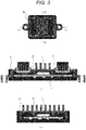
- the configuration of a second embodiment will be described in comparison with the first embodiment. While the first embodiment is a case where the electromagnetic shield unit 8 covers an entire periphery of the side surface of the control substrate 2, the second embodiment has a structure in which an outer periphery of the electronic component 1 is surrounded by a frame body 14 extending from the housing case 3 toward the control substrate 2 in addition to covering the entire periphery of the side surface of the control substrate 2, as illustrated in FIG. 3 . By doubly covering the outer periphery of the control substrate 2 and the outer periphery of the electronic component 1, it is possible to further enhance electromagnetic shielding property.
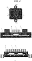
- the configuration of a third embodiment will be described in comparison with the first embodiment. While the first embodiment has a structure in which the electromagnetic shield unit 8 covers the entire periphery of the side surface of the control substrate 2, the third embodiment is configured such that the electromagnetic shield unit 8 covers the control substrate 2 on two side surfaces out of four side surfaces as illustrated in FIG. 4(b) similarly to the first embodiment, while the electronic component 1 is covered by a region smaller than a width of the control substrate 2 on the other two sides as illustrated in FIG. 4(a) .
- the present embodiment is effective when it is judged that there is no need to cover the entire periphery of the side surface of the control substrate 2 with the housing case 3 after examination of desired electromagnetic shielding property. With this configuration, it is possible to reduce material cost by reducing the capacity of the housing case 3 while maintaining the electromagnetic shielding performance.
- the configuration of a fourth embodiment will be described in comparison with the first embodiment. While the first embodiment is a case where the electromagnetic shield unit 8 covers the entire periphery of the side surface of the control substrate 2, the fourth embodiment has a structure in which the outer periphery of the electronic component 1 is surrounded by the frame body 14 extending from the housing case 3 toward the control substrate 2 within a region smaller than the width of the control substrate 2 as illustrated in FIG. 5 .
- the present embodiment is effective when it is judged that there is no need to cover the entire periphery of the side surface of the control substrate 2 with the housing case 3 after examination of desired electromagnetic shielding property. With this configuration, it is possible to reduce material cost by reducing the capacity of the housing case 3 while maintaining the electromagnetic shielding performance.
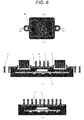
- the configuration of a fifth embodiment will be described in comparison with the first embodiment. While the first embodiment is a case where the housing case 3 is integrally molded together with the heat sink 7 having the heat dissipation fin 6, the electromagnetic shield unit 8 that shields electromagnetic noise, and the fixture for vehicle mounting 9 for fixing the electronic control device to a vehicle, the fifth embodiment has a structure in which the heat sink 7 and the fixture for vehicle mounting 9 are integrally molded as illustrated in FIG. 6 .
- the present embodiment is effective when it is judged that the desired electromagnetic shielding performance can be satisfied with a configuration in which the electronic component 1 is surrounded from vertical directions by the housing case 3 and the wiring layer of the control substrate 2 without covering entire periphery of the side surface of the control substrate 2 by the housing case 3. With this configuration, it is possible to reduce material cost by reducing the capacity of the housing case 3 while maintaining the electromagnetic shielding performance.
- the configuration of a sixth embodiment will be described in comparison with the first embodiment. While the first embodiment is a case where the housing case 3 is integrally molded together with the heat sink 7 having the heat dissipation fin 6, the electromagnetic shield unit 8 that shields electromagnetic noise, and the fixture for vehicle mounting 9 for fixing the electronic control device to a vehicle, the sixth embodiment has a structure in which the electromagnetic shield unit 8 and the fixture for vehicle mounting 9 are integrally molded as illustrated in FIG. 7 . With the fixture for vehicle mounting 9 integrally molded with the housing case 3, heat dissipated from the electronic component 1 towards the housing case 3 such as the electromagnetic shield unit 8 can be dissipated to the vehicle body via the fixture for vehicle mounting 9. The present embodiment is effective when it is judged that the heat dissipation performance can be satisfied with no heat dissipation fin 6, whereby the material cost can be reduced by reducing the capacity of the housing case 3.
Landscapes
- Engineering & Computer Science (AREA)
- Microelectronics & Electronic Packaging (AREA)
- Physics & Mathematics (AREA)
- Thermal Sciences (AREA)
- Manufacturing & Machinery (AREA)
- Electromagnetism (AREA)
- Mechanical Engineering (AREA)
- Shielding Devices Or Components To Electric Or Magnetic Fields (AREA)
- Cooling Or The Like Of Electrical Apparatus (AREA)
- Cooling Or The Like Of Semiconductors Or Solid State Devices (AREA)
Abstract
Description
- The present invention relates to an electronic control device such as an engine control unit and an automatic transmission control unit used for an automobile, and particularly to a casing structure of the electronic control device.
- With the background of environmental and energy problems, the trend of automobile electronics is accelerating, and the number of electronic control devices installed has been greatly increasing. This leads to limitation of installation space for the electronic control devices, and thus, the electronic control devices are inevitably installed in an engine compartment with severe environmental conditions compared with other locations of an automobile. On the other hand, with a trend of an expanded cabin space to achieve enhanced comfortability of an automobile, the engine compartment has been downsized. This necessitates arrangement of a large number of electronic control devices and wire harnesses in a downsized engine compartment, leading to a difficulty in layout, an increase in weight, and increase in cost. This generates a demand for an electronic control device that is smaller, lighter, and lower in cost. In addition, the wire harness tends to be shortened. This results in, for example, installation of the engine control device at a position closer to the engine, leading to a concern about an influence of high heat and high vibration of the engine on the engine control device. To cope with this, there is a need to enhance heat resistance and vibration resistance of the electronic control device. As a countermeasure, there is a known structure in which a control substrate on which electronic components are mounted is sealed with resin (see PTL 1).
- An electric and electronic module described in
PTL 1 includes an electronic circuit board on which an electronic circuit is mounted and a metal base for mounting the electronic circuit board, and the electronic circuit board is sealed with a resin. - PTL 1:
JP 2007-273796 A - By sealing the electronic circuit board with a resin, however, there is concern of a decrease in shielding property against electromagnetic noise in comparison with a metal cover. Electromagnetic noise has an influence on an electronic control device and causes, for example, the device to malfunction by the noise generated from on-vehicle components such as an engine, a motor, or the like, or from equipment such as a car radio using external radio-frequency equipment. In addition, the electronic control device might be a noise source in some cases and might cause malfunction of a vehicle-mounted receiving device such as a television receiver, GPS, and Bluetooth (registered trademark). While it is conceivable to add components to enhance shielding property as countermeasures, adding components would inevitably increase the cost.
- This makes it a problem to provide an electronic control device excellent in electromagnetic shielding property with low cost.
- In order to solve the above-described problem, an electronic control device according to the present invention includes: an electronic component; a control substrate on which the electronic component is mounted; a sealing resin that seals at least a portion of the control substrate; a metal member sealed with the sealing resin, in which the metal member includes a heat sink portion a portion of which is exposed from the sealing resin to dissipate heat of the inside of the sealing resin; a protection portion that covers the electronic component; and a fixing portion a portion of which is exposed from the sealing resin to achieve fixation to a vehicle body.
- According to the present invention, it is possible to provide an electronic control device excellent in electromagnetic shielding property with low cost.
-
- [
FIG. 1] FIG. 1 is a cross-sectional view of an electronic control device. - [
FIG. 2] FIG. 2 is a configuration and an assembly procedure of an electronic control device of a first embodiment. - [
FIG. 3] FIG. 3 is a configuration of an electronic control device of a second embodiment. - [
FIG. 4] FIG. 4 is a configuration of an electronic control device of a third embodiment. - [
FIG. 5] FIG. 5 is a configuration of an electronic control device of a fourth embodiment. - [
FIG. 6] FIG. 6 is a configuration of an electronic control device of a fifth embodiment. - [
FIG. 7] FIG. 7 is a configuration of an electronic control device of a sixth embodiment. - Hereinafter, a configuration and an assembly procedure of an electronic control device according to specific embodiments of the present invention will be described with reference to the accompanying drawings.
-
FIG. 1 is a cross-sectional view illustrating a control device according to the first embodiment.FIG. 2 is a configuration and an assembly procedure of the control device illustrated inFIG. 1 . - As illustrated in
FIGS. 1 and2 , anelectronic control device 30 according to the present invention includes acontrol substrate 2 on which anelectronic component 1 such as a microcomputer is mounted, ahousing case 3, aconnector 4, and asealing resin 5. - As illustrated in
FIG. 2(a) , thehousing case 3 may be integrally molded together with aheat sink 7 having a heat dissipation fin 6 for dissipating heat generated from electronic components to the outside of theelectronic control device 30, anelectromagnetic shield unit 8 that shields electromagnetic noise, and a fixture for vehicle mounting 9 for fixing the electronic control device to a vehicle. The material is preferably a metal member having high thermal conductivity, shielding property and rigidity, and it is preferable to use aluminum or an aluminum alloy from the viewpoints of mass productivity, weight reduction, heat dissipation property, and cost. By integrating theheat sink 7, theshield unit 8, and the fixture for vehicle mounting 9 in this manner, it is possible to reduce the number of components, leading to cost reduction and enhancement of productivity. - With the fixture for vehicle mounting 9 integrally molded with the
housing case 3, heat dissipated from theelectronic component 1 towards thehousing case 3 such as theheat sink 7 can be dissipated to the vehicle body via the fixture for vehicle mounting 9. - As illustrated in
FIG. 2(b) , theconnector 4 is formed by fabricating aconnector unit assembly 12 constituted with aterminal 10 for connecting a vehicle-side harness with thecontrol substrate 2, and a fixing plate 11 for aligning and holding theterminals 10 at a prescribed pitch. The fixing plate 11 includes pins 13 for increasing insertability into thehousing case 3 to be described below and for facilitating positioning. The number of the pins 13 is preferably two or more. The material of theterminal 10 may preferably be copper or a copper alloy from the viewpoint of conductivity, downsizing, and cost. The material of the fixing plate 11 may preferably be a polybutylene terephthalate (PBT) resin, a polyamide (PA) 66 resin, and a polyphenylene sulfide (PPS) resin from the viewpoint of light weight and excellent heat resistance. - Subsequently, as illustrated in
FIG. 2(c) , thehousing case 3 and theconnector unit assembly 12 are assembled to each other. At that time, the pins 13 of theconnector unit assembly 12 are inserted into mutually opposing penetration holes on thehousing case 3, and the fixing plate 11 is brought into contact with thehousing case 3, thereby positioning theconnector unit assembly 12 and thehousing case 3. - When the position of the
connector unit assembly 12 with respect to thehousing case 3 is determined, tips of the pins 13 protruding from thehousing case 3 are fixed by thermal caulking as illustrated inFIG. 2(d) . - After the
connector unit assembly 12 is fixed, thecontrol substrate 2 on which theelectronic component 1 such as a microcomputer is mounted is assembled to thedie casting case 3 as illustrated inFIGS. 2(e) and 2(f) . At that time, an electronic component susceptible to external electromagnetic noise and an electronic component likely to generate electromagnetic noise, such as a microcomputer and a quartz oscillator, are mounted on a surface of thecontrol substrate 2 facing thehousing case 3. This configuration enables theelectronic component 1 to be surrounded by wiring layers of thehousing case 3 and thecontrol substrate 2, leading to enhancement of the electromagnetic shielding property. In order to further enhance the electromagnetic shielding property, it is preferable to provide a solid pattern in one layer of the wiring layers of the control substrate or in the periphery where theelectronic component 1 is mounted. This makes it possible to also enhance the shielding property against electromagnetic noise from the surface not facing thehousing case 3. - A resin wiring board based on glass epoxy resin or the like is used as the
control substrate 2. In connecting theelectronic component 1 to thecontrol substrate 2, a lead-free solder such as Sn-Cu solder, Sn-Ag-Cu solder, and Sn-Ag-Cu-Bi solder is applied. By setting thecontrol substrate 2 on a substrate receiving unit (not illustrated) of thehousing case 3, the position in a height direction is determined, and subsequently thecontrol substrate 2 is fixed to thehousing case 3 using screws (not illustrated). The number of fixation points by screws may preferably be three or more. In connecting theterminal 10 of theconnector unit assembly 12 with thecontrol substrate 2, a lead-free solder such as Sn-Cu solder, Sn-Ag-Cu solder, and Sn-Ag-Cu-Bi solder is applied to a through hole portion 17 of thecontrol substrate 2, into which theterminal 10 is inserted, so as to achieve connection. Note that the type of theconnector 4 may be a surface mounting type or a press fit type. - What is important here is a method of fixing the
connector unit assembly 12. Specifically, in a case where theconnector unit assembly 12 is fixed to thecontrol substrate 2 instead of thehousing case 3, the positioning pin 13 is to be inserted into thecontrol substrate 2. This would generate a need to provide a penetration hole for the positioning pin 13 on thecontrol substrate 2, and increase the substrate area correspondingly. In addition, in a case where theterminal 10 of theconnector unit assembly 12 and the through hole portion 17 of thecontrol substrate 2 are joined with each other, theconnector unit assembly 12 and thecontrol substrate 2 individually expand and contract due to a thermal history by joining. In this process, however, there is a difference in the amount of expansion and contraction between theconnector unit assembly 12 and thecontrol substrate 2, leading to generation of warping in theconnector unit assembly 12 and thecontrol substrate 2 after joining. Furthermore, due to greater rigidity of thehousing base 3 and the flat shape of a substrate receiving surface, fixing theconnector unit assembly 12 and thecontrol substrate 2 joined with each other to thehousing base 3 would bring the warping of theconnector unit assembly 12 and thecontrol substrate 2 with low rigidity back to a former state. This would generate a peeling stress in a joint portion between the terminal 10 and the through hole portion 17. - To cope with this problem, as described in the embodiment, the method of fixing the
connector unit assembly 12 may preferably include first fixing theconnector unit assembly 12 to thehousing case 3, and thereafter joining theterminal 10 of theconnector unit assembly 12 to the through hole portion 17 of thecontrol substrate 2. By additionally implementing this method, it is possible to further suppress the warping of theconnector unit assembly 12 and thecontrol substrate 2, and also to suppress generation of stress at the joint portion between the terminal 10 and the through hole portion 17. - As illustrated in
FIG. 2(g) , a sub-assembly 20 fabricated in this manner is set in a mold for resin sealing. In the present embodiment, the sub-assembly is set on anupper die 18 that is a movable die, then the upper die is moved and set onto a lower die 19 as a fixed die. The fin portion 6 of thehousing cover 3 to be desirably exposed from theresin 5 after resin sealing and the fixture for vehicle mounting 9 have a structure to be held by a mold in order to prevent entry of resin during resin molding. - For the purpose of ensuring the fluidity of the sealing
resin 5 and enabling the resin to fill over narrower sites inside of the mold, it is preferable to preheat the mold, the sub-assembly, and the resin. The sealingresin 5 may be a thermosetting epoxy resin, an unsaturated polyester resin, or a thermoplastic resin. Examples of sealing methods include transfer molding, compression molding, injection molding, and hot melt. Physical property values of the sealingresin 5 are desirably such that the linear expansion coefficient is 10 to 30 × 10-6/°C, the thermal conductivity is 0.5 to 3 W/mK. - After completion of resin filling into the mold, the sealing
resin 5 is cured in the mold. After curing, the mold is opened and the resin molded product is taken out to complete fabrication of theelectronic control device 30 illustrated inFIG. 2 (h) . - Note that a rising
portion 22 on the outer periphery of the housing case excluding the fixture for vehicle mounting 9 is preferably covered with the sealingresin 5. This configuration increases the contact area between thehousing case 3 and the sealingresin 5, making it possible to enhance waterproof/anti-saline reliability. Since this configuration further enables reduction of expansion and shrinkage of thehousing case 3, it is possible to enhance waterproof and anti-saline reliability and solder connection reliability. - Moreover, the surface of the
housing case 3 and the surface of the sealingresin 5 may preferably be on a same surface at acontact end 23 of thehousing case 3 and the sealingresin 5. This makes it possible to suppress accumulation of water, salt water, and foreign matter at thecontact end 23. - In addition, it is further preferable to cover the thermal caulking portion of the connector terminal fixing plate 11 with the sealing
resin 5. - This makes it possible to suppress deterioration of the thermal caulking portion and suppress entry of water and salt water from the thermal caulking portion.
- Finally, a
housing 21 of theconnector 4 is also integrally molded with the sealingresin 5. This can omit necessity to provide the connector housing as a separate component, leading to reduction of the number of components, and probably leading to a cost advantage and productivity enhancement. - The configuration of a second embodiment will be described in comparison with the first embodiment. While the first embodiment is a case where the
electromagnetic shield unit 8 covers an entire periphery of the side surface of thecontrol substrate 2, the second embodiment has a structure in which an outer periphery of theelectronic component 1 is surrounded by aframe body 14 extending from thehousing case 3 toward thecontrol substrate 2 in addition to covering the entire periphery of the side surface of thecontrol substrate 2, as illustrated inFIG. 3 . By doubly covering the outer periphery of thecontrol substrate 2 and the outer periphery of theelectronic component 1, it is possible to further enhance electromagnetic shielding property. - The configuration of a third embodiment will be described in comparison with the first embodiment. While the first embodiment has a structure in which the
electromagnetic shield unit 8 covers the entire periphery of the side surface of thecontrol substrate 2, the third embodiment is configured such that theelectromagnetic shield unit 8 covers thecontrol substrate 2 on two side surfaces out of four side surfaces as illustrated inFIG. 4(b) similarly to the first embodiment, while theelectronic component 1 is covered by a region smaller than a width of thecontrol substrate 2 on the other two sides as illustrated inFIG. 4(a) . The present embodiment is effective when it is judged that there is no need to cover the entire periphery of the side surface of thecontrol substrate 2 with thehousing case 3 after examination of desired electromagnetic shielding property. With this configuration, it is possible to reduce material cost by reducing the capacity of thehousing case 3 while maintaining the electromagnetic shielding performance. - The configuration of a fourth embodiment will be described in comparison with the first embodiment. While the first embodiment is a case where the
electromagnetic shield unit 8 covers the entire periphery of the side surface of thecontrol substrate 2, the fourth embodiment has a structure in which the outer periphery of theelectronic component 1 is surrounded by theframe body 14 extending from thehousing case 3 toward thecontrol substrate 2 within a region smaller than the width of thecontrol substrate 2 as illustrated inFIG. 5 . The present embodiment is effective when it is judged that there is no need to cover the entire periphery of the side surface of thecontrol substrate 2 with thehousing case 3 after examination of desired electromagnetic shielding property. With this configuration, it is possible to reduce material cost by reducing the capacity of thehousing case 3 while maintaining the electromagnetic shielding performance. - The configuration of a fifth embodiment will be described in comparison with the first embodiment. While the first embodiment is a case where the
housing case 3 is integrally molded together with theheat sink 7 having the heat dissipation fin 6, theelectromagnetic shield unit 8 that shields electromagnetic noise, and the fixture for vehicle mounting 9 for fixing the electronic control device to a vehicle, the fifth embodiment has a structure in which theheat sink 7 and the fixture for vehicle mounting 9 are integrally molded as illustrated inFIG. 6 . The present embodiment is effective when it is judged that the desired electromagnetic shielding performance can be satisfied with a configuration in which theelectronic component 1 is surrounded from vertical directions by thehousing case 3 and the wiring layer of thecontrol substrate 2 without covering entire periphery of the side surface of thecontrol substrate 2 by thehousing case 3. With this configuration, it is possible to reduce material cost by reducing the capacity of thehousing case 3 while maintaining the electromagnetic shielding performance. - The configuration of a sixth embodiment will be described in comparison with the first embodiment. While the first embodiment is a case where the
housing case 3 is integrally molded together with theheat sink 7 having the heat dissipation fin 6, theelectromagnetic shield unit 8 that shields electromagnetic noise, and the fixture for vehicle mounting 9 for fixing the electronic control device to a vehicle, the sixth embodiment has a structure in which theelectromagnetic shield unit 8 and the fixture for vehicle mounting 9 are integrally molded as illustrated inFIG. 7 . With the fixture for vehicle mounting 9 integrally molded with thehousing case 3, heat dissipated from theelectronic component 1 towards thehousing case 3 such as theelectromagnetic shield unit 8 can be dissipated to the vehicle body via the fixture for vehicle mounting 9. The present embodiment is effective when it is judged that the heat dissipation performance can be satisfied with no heat dissipation fin 6, whereby the material cost can be reduced by reducing the capacity of thehousing case 3. - As above, embodiments of the control device according to the present invention have been described. The present invention is not limited to the above-described embodiments but may include various design modifications without departing from the spirit according to the present invention described in claims.
-
- 1 electronic component
- 2 control substrate
- 3 housing case
- 4 connector
- 5 sealing resin
- 5a sealing resin to cover heat dissipation fin
- 5b sealing resin to cover rising portion of outer periphery
- of housing case
- 6 heat dissipation fin
- 7 heat sink
- 8 electromagnetic shield unit
- 9 fixture for vehicle mounting
- 10 terminal
- 11 fixing plate
- 12 connector unit assembly
- 13 pin
- 14 frame body
- 17 through hole portion
- 18 upper mold
- 19 lower mold
- 20 sub-assembly
- 21 connector housing
- 22 rising portion of outer periphery of housing case
- 23 contact end of housing case and sealing resin
- 24 penetration hole
- 25 mold
- 30 electronic control device
Claims (13)
- An electronic control device comprising:an electronic component;a control substrate on which the electronic component is mounted;a sealing resin that seals at least a portion of the control substrate;a metal member sealed with the sealing resin,wherein the metal member includes:a heat sink portion a portion of which is exposed from the sealing resin to dissipate heat of the inside of the sealing resin;a shield unit that shields the electronic component; anda fixing portion a portion of which is exposed from the sealing resin to achieve fixation to a vehicle body.
- The electronic control device according to claim 1,
wherein the shield unit is an electromagnetic shield unit that shields electromagnetic noise emitted between the electronic component and an external space. - The electronic control device according to claim 2,
wherein the metal member forms the electromagnetic shield unit on an outer periphery of the heat sink portion, and
forms the fixing portion on an outer periphery of the electromagnetic shield unit. - The electronic control device according to any one of claims 2 and 3,
wherein the heat sink portion has a heat dissipation fin, and the heat dissipation fin is exposed from the sealing resin. - The electronic control device according to any one of claims 2 to 4,
wherein the metal member has a rising portion on the outer periphery of the heat sink portion and forms the electromagnetic shield unit by forming an outline in a recessed shape. - The electronic control device according to claim 5, wherein the control substrate is housed in the portion with a recessed shape.
- The electronic control device according to any one of claims 1 to 6,
wherein the electronic component is mounted on a surface of the control substrate facing the metal member. - The electronic control device according to claim 7,
wherein at least a microcomputer and a quartz oscillator among the electronic components are mounted on the surface of the control substrate facing the metal member. - The electronic control device according to any one of claims 7 and 8,
wherein a frame body protruding from the housing case is formed on an outer periphery of the electronic component mounted on a surface of the control substrate facing the housing case. - The electronic control device according to any one of claims 1 to 9, wherein a material of the metal member is one of aluminum and an aluminum alloy.
- An electronic control device comprising:an electronic component;a control substrate on which the electronic component is mounted;a sealing resin that seals at least a portion of the control substrate; anda metal member sealed with the sealing resin,wherein the metal member includes:a heat sink portion a portion of which is exposed from the sealing resin to dissipate heat of the inside of the sealing resin; anda fixing portion a portion of which is exposed from the sealing resin to achieve fixation to a vehicle body,the heat sink portion and the fixing portion are integrally molded, andthe electronic component is mounted on a surface of the control substrate facing the metal member.
- An electronic control device comprising:an electronic component;a control substrate on which the electronic component is mounted;a sealing resin that seals at least a portion of the control substrate; anda metal member sealed with the sealing resin,wherein the metal member includes:an electromagnetic shield unit that shields electromagnetic noise emitted between the electronic component and an external space; anda fixing portion a portion of which is exposed from the sealing resin to achieve fixation to a vehicle body, andthe electromagnetic shield unit and the fixing portion are integrally molded, andthe electronic component is mounted on a surface of the control substrate facing the metal member.
- The electronic control device according to any one of claims 7, 11, and 12,
wherein the control substrate includes a solid pattern in at least one layer or in a region where the electronic component is provided.
Applications Claiming Priority (2)
| Application Number | Priority Date | Filing Date | Title |
|---|---|---|---|
| JP2015190619 | 2015-09-29 | ||
| PCT/JP2016/073032 WO2017056727A1 (en) | 2015-09-29 | 2016-08-05 | Electronic control device |
Publications (2)
| Publication Number | Publication Date |
|---|---|
| EP3358925A1 true EP3358925A1 (en) | 2018-08-08 |
| EP3358925A4 EP3358925A4 (en) | 2019-05-22 |
Family
ID=58423498
Family Applications (1)
| Application Number | Title | Priority Date | Filing Date |
|---|---|---|---|
| EP16850904.0A Withdrawn EP3358925A4 (en) | 2015-09-29 | 2016-08-05 | ELECTRONIC CONTROL DEVICE |
Country Status (5)
| Country | Link |
|---|---|
| US (1) | US20180220539A1 (en) |
| EP (1) | EP3358925A4 (en) |
| JP (1) | JPWO2017056727A1 (en) |
| CN (1) | CN108029228A (en) |
| WO (1) | WO2017056727A1 (en) |
Cited By (1)
| Publication number | Priority date | Publication date | Assignee | Title |
|---|---|---|---|---|
| EP3578017A1 (en) * | 2017-02-01 | 2019-12-11 | Robert Bosch GmbH | Control unit and method for production thereof |
Families Citing this family (7)
| Publication number | Priority date | Publication date | Assignee | Title |
|---|---|---|---|---|
| DE102015206616A1 (en) * | 2015-04-14 | 2016-10-20 | Zf Friedrichshafen Ag | Printed circuit board for electronic function control for a vehicle |
| CN110087851B (en) * | 2016-12-22 | 2024-04-12 | 日立安斯泰莫株式会社 | Electronic control device |
| JP7381219B2 (en) * | 2019-04-23 | 2023-11-15 | 日立Astemo株式会社 | electronic control unit |
| CN113841469B (en) * | 2019-05-31 | 2024-01-02 | 日立安斯泰莫株式会社 | electronic control device |
| CN115175519A (en) * | 2019-08-30 | 2022-10-11 | 华为技术有限公司 | Radiator, electronic equipment and car |
| US12167536B2 (en) * | 2020-03-10 | 2024-12-10 | Rohm Co., Ltd. | Electronic device |
| JP7607430B2 (en) * | 2020-10-12 | 2024-12-27 | 株式会社マキタ | Work Machine |
Family Cites Families (43)
| Publication number | Priority date | Publication date | Assignee | Title |
|---|---|---|---|---|
| JPS5413545Y2 (en) * | 1974-12-09 | 1979-06-08 | ||
| JPH04261097A (en) * | 1991-01-25 | 1992-09-17 | Mitsubishi Electric Corp | Multilayer printed board |
| US5598034A (en) * | 1992-07-22 | 1997-01-28 | Vlsi Packaging Corporation | Plastic packaging of microelectronic circuit devices |
| US6180045B1 (en) * | 1998-05-20 | 2001-01-30 | Delco Electronics Corporation | Method of forming an overmolded electronic assembly |
| JP4121185B2 (en) * | 1998-06-12 | 2008-07-23 | 新電元工業株式会社 | Electronic circuit equipment |
| JP3032505B1 (en) * | 1998-10-19 | 2000-04-17 | 北川工業株式会社 | heatsink |
| JP4234259B2 (en) * | 1999-05-14 | 2009-03-04 | 富士通テン株式会社 | Combination structure of electronic equipment |
| JP2002134970A (en) * | 2000-10-26 | 2002-05-10 | Denso Corp | Electronic control unit |
| JP2003332771A (en) * | 2002-05-10 | 2003-11-21 | Denso Corp | Electronic control unit |
| US7492600B2 (en) * | 2003-11-14 | 2009-02-17 | Tyco Electronics Corporation | Sealed header and method of making |
| US7120024B2 (en) * | 2004-02-27 | 2006-10-10 | Fujitsu Ten Limited | Electronic control device |
| JP4379288B2 (en) * | 2004-06-02 | 2009-12-09 | 株式会社デンソー | Electronic device housing structure |
| DE102004043019A1 (en) * | 2004-09-06 | 2006-03-23 | eupec Europäische Gesellschaft für Leistungshalbleiter mbH | module |
| JP2007066994A (en) * | 2005-08-29 | 2007-03-15 | Auto Network Gijutsu Kenkyusho:Kk | Shield conductor |
| US7582951B2 (en) * | 2005-10-20 | 2009-09-01 | Broadcom Corporation | Methods and apparatus for improved thermal performance and electromagnetic interference (EMI) shielding in leadframe integrated circuit (IC) packages |
| US20070200210A1 (en) * | 2006-02-28 | 2007-08-30 | Broadcom Corporation | Methods and apparatus for improved thermal performance and electromagnetic interference (EMI) shielding in integrated circuit (IC) packages |
| CN100477176C (en) * | 2006-06-01 | 2009-04-08 | 美国博通公司 | Integrated circuit package and assembling method thereof |
| US7808087B2 (en) * | 2006-06-01 | 2010-10-05 | Broadcom Corporation | Leadframe IC packages having top and bottom integrated heat spreaders |
| JP4870509B2 (en) * | 2006-09-27 | 2012-02-08 | 新光電気工業株式会社 | Electronic equipment |
| JP4702311B2 (en) * | 2007-03-19 | 2011-06-15 | トヨタ自動車株式会社 | Electrical unit with a capacitor |
| JP4512626B2 (en) * | 2007-09-28 | 2010-07-28 | 日立オートモティブシステムズ株式会社 | Car electronics |
| JP5117843B2 (en) * | 2007-12-27 | 2013-01-16 | 三菱重工業株式会社 | Inverter-integrated electric compressor |
| JP4884406B2 (en) * | 2008-01-28 | 2012-02-29 | 日立オートモティブシステムズ株式会社 | Resin-sealed electronic module and resin-sealing molding method thereof |
| JP2010192759A (en) * | 2009-02-19 | 2010-09-02 | Sanyo Electric Co Ltd | Electromagnetic shield structure of electronic apparatus housing |
| JP2011054640A (en) * | 2009-08-31 | 2011-03-17 | Funai Electric Co Ltd | Shield package substrate |
| JP5165012B2 (en) * | 2010-02-22 | 2013-03-21 | 三菱電機株式会社 | Resin-sealed electronic control device and manufacturing method thereof |
| JP4948613B2 (en) * | 2010-02-25 | 2012-06-06 | 三菱電機株式会社 | Resin-sealed electronic control device and manufacturing method thereof |
| DE102010002765A1 (en) * | 2010-03-11 | 2011-09-15 | Robert Bosch Gmbh | Housing base of a multi-part housing and method for mounting a housing |
| JP2011216849A (en) * | 2010-03-17 | 2011-10-27 | Tdk Corp | Electronic circuit module component, and method of manufacturing the same |
| JP5014470B2 (en) * | 2010-06-28 | 2012-08-29 | 三菱電機株式会社 | Resin-sealed electronic control device and manufacturing method thereof |
| JP5463235B2 (en) * | 2010-07-30 | 2014-04-09 | 日立オートモティブシステムズ株式会社 | Substrate structure used for in-vehicle electronic devices |
| DE102012204145A1 (en) * | 2012-03-16 | 2013-09-19 | Continental Automotive Gmbh | Housing cover for receiving plug modules |
| JP5990418B2 (en) * | 2012-07-06 | 2016-09-14 | 日立オートモティブシステムズ株式会社 | On-vehicle electronic control device and manufacturing method thereof |
| WO2014020783A1 (en) * | 2012-07-30 | 2014-02-06 | パナソニック株式会社 | Semiconductor device provided with radiating structure |
| JP5528641B1 (en) * | 2012-10-03 | 2014-06-25 | 新電元工業株式会社 | Electronics |
| JP2014216326A (en) * | 2013-04-22 | 2014-11-17 | 株式会社デンソー | Electronic device and method of manufacturing the same |
| CN105247331A (en) * | 2013-05-01 | 2016-01-13 | 索尼公司 | Sensor device and electronic apparatus |
| JP6282432B2 (en) * | 2013-09-26 | 2018-02-21 | 株式会社東芝 | Electronics |
| WO2015050145A1 (en) * | 2013-10-02 | 2015-04-09 | 日立オートモティブシステムズ株式会社 | Electronic control device |
| US9480143B2 (en) * | 2013-10-09 | 2016-10-25 | Uusi, Llc | Motor control device |
| EP3119172A4 (en) * | 2014-03-14 | 2017-11-15 | Kaneka Corporation | Electronic terminal device and method for assembling same |
| JP5943985B2 (en) * | 2014-10-30 | 2016-07-05 | 三菱電機株式会社 | Electronic control unit |
| JP6669586B2 (en) * | 2016-05-26 | 2020-03-18 | 新光電気工業株式会社 | Semiconductor device and method of manufacturing semiconductor device |
-
2016
- 2016-08-05 WO PCT/JP2016/073032 patent/WO2017056727A1/en not_active Ceased
- 2016-08-05 EP EP16850904.0A patent/EP3358925A4/en not_active Withdrawn
- 2016-08-05 US US15/747,569 patent/US20180220539A1/en not_active Abandoned
- 2016-08-05 JP JP2017542990A patent/JPWO2017056727A1/en active Pending
- 2016-08-05 CN CN201680053998.9A patent/CN108029228A/en active Pending
Cited By (1)
| Publication number | Priority date | Publication date | Assignee | Title |
|---|---|---|---|---|
| EP3578017A1 (en) * | 2017-02-01 | 2019-12-11 | Robert Bosch GmbH | Control unit and method for production thereof |
Also Published As
| Publication number | Publication date |
|---|---|
| WO2017056727A1 (en) | 2017-04-06 |
| JPWO2017056727A1 (en) | 2018-02-22 |
| US20180220539A1 (en) | 2018-08-02 |
| EP3358925A4 (en) | 2019-05-22 |
| CN108029228A (en) | 2018-05-11 |
Similar Documents
| Publication | Publication Date | Title |
|---|---|---|
| US20180220539A1 (en) | Electronic Control Device | |
| EP3358919B1 (en) | Electronic control device and manufacturing method for same | |
| US10881014B2 (en) | Electronic control device, and manufacturing method for vehicle-mounted electronic control device | |
| US10829064B2 (en) | Electronic control device | |
| EP3346810B1 (en) | Vehicle-mounted control device | |
| CN104956547B (en) | Vehicle-mounted electronic building brick | |
| JP6472462B2 (en) | Electronic control unit | |
| CN109479381B (en) | Electronic control device and assembling method thereof | |
| US10986741B2 (en) | Electronic control device | |
| JP4864742B2 (en) | Modular equipment | |
| JP2009049109A (en) | Modular equipment |
Legal Events
| Date | Code | Title | Description |
|---|---|---|---|
| STAA | Information on the status of an ep patent application or granted ep patent |
Free format text: STATUS: THE INTERNATIONAL PUBLICATION HAS BEEN MADE |
|
| PUAI | Public reference made under article 153(3) epc to a published international application that has entered the european phase |
Free format text: ORIGINAL CODE: 0009012 |
|
| STAA | Information on the status of an ep patent application or granted ep patent |
Free format text: STATUS: REQUEST FOR EXAMINATION WAS MADE |
|
| 17P | Request for examination filed |
Effective date: 20180323 |
|
| AK | Designated contracting states |
Kind code of ref document: A1 Designated state(s): AL AT BE BG CH CY CZ DE DK EE ES FI FR GB GR HR HU IE IS IT LI LT LU LV MC MK MT NL NO PL PT RO RS SE SI SK SM TR |
|
| AX | Request for extension of the european patent |
Extension state: BA ME |
|
| DAV | Request for validation of the european patent (deleted) | ||
| DAX | Request for extension of the european patent (deleted) | ||
| A4 | Supplementary search report drawn up and despatched |
Effective date: 20190418 |
|
| RIC1 | Information provided on ipc code assigned before grant |
Ipc: H05K 5/06 20060101ALI20190412BHEP Ipc: B60R 16/02 20060101ALI20190412BHEP Ipc: H05K 7/14 20060101ALI20190412BHEP Ipc: H01L 23/29 20060101ALI20190412BHEP Ipc: H05K 5/00 20060101ALI20190412BHEP Ipc: H05K 1/18 20060101ALI20190412BHEP Ipc: H05K 9/00 20060101AFI20190412BHEP Ipc: H05K 1/02 20060101ALI20190412BHEP Ipc: H05K 7/20 20060101ALI20190412BHEP Ipc: H05K 3/28 20060101ALI20190412BHEP |
|
| STAA | Information on the status of an ep patent application or granted ep patent |
Free format text: STATUS: THE APPLICATION HAS BEEN WITHDRAWN |
|
| 18W | Application withdrawn |
Effective date: 20191119 |