EP3358637A1 - Multi-junction photoelectric conversion device and photoelectric conversion module - Google Patents
Multi-junction photoelectric conversion device and photoelectric conversion module Download PDFInfo
- Publication number
- EP3358637A1 EP3358637A1 EP16851817.3A EP16851817A EP3358637A1 EP 3358637 A1 EP3358637 A1 EP 3358637A1 EP 16851817 A EP16851817 A EP 16851817A EP 3358637 A1 EP3358637 A1 EP 3358637A1
- Authority
- EP
- European Patent Office
- Prior art keywords
- photoelectric conversion
- layer
- conversion unit
- refractive index
- intermediate layer
- Prior art date
- Legal status (The legal status is an assumption and is not a legal conclusion. Google has not performed a legal analysis and makes no representation as to the accuracy of the status listed.)
- Pending
Links
Images
Classifications
-
- H—ELECTRICITY
- H10—SEMICONDUCTOR DEVICES; ELECTRIC SOLID-STATE DEVICES NOT OTHERWISE PROVIDED FOR
- H10K—ORGANIC ELECTRIC SOLID-STATE DEVICES
- H10K30/00—Organic devices sensitive to infrared radiation, light, electromagnetic radiation of shorter wavelength or corpuscular radiation
- H10K30/50—Photovoltaic [PV] devices
- H10K30/57—Photovoltaic [PV] devices comprising multiple junctions, e.g. tandem PV cells
-
- H—ELECTRICITY
- H01—ELECTRIC ELEMENTS
- H01G—CAPACITORS; CAPACITORS, RECTIFIERS, DETECTORS, SWITCHING DEVICES, LIGHT-SENSITIVE OR TEMPERATURE-SENSITIVE DEVICES OF THE ELECTROLYTIC TYPE
- H01G9/00—Electrolytic capacitors, rectifiers, detectors, switching devices, light-sensitive or temperature-sensitive devices; Processes of their manufacture
- H01G9/20—Light-sensitive devices
- H01G9/2004—Light-sensitive devices characterised by the electrolyte, e.g. comprising an organic electrolyte
- H01G9/2009—Solid electrolytes
-
- H—ELECTRICITY
- H10—SEMICONDUCTOR DEVICES; ELECTRIC SOLID-STATE DEVICES NOT OTHERWISE PROVIDED FOR
- H10F—INORGANIC SEMICONDUCTOR DEVICES SENSITIVE TO INFRARED RADIATION, LIGHT, ELECTROMAGNETIC RADIATION OF SHORTER WAVELENGTH OR CORPUSCULAR RADIATION
- H10F10/00—Individual photovoltaic cells, e.g. solar cells
- H10F10/10—Individual photovoltaic cells, e.g. solar cells having potential barriers
- H10F10/16—Photovoltaic cells having only PN heterojunction potential barriers
- H10F10/161—Photovoltaic cells having only PN heterojunction potential barriers comprising multiple PN heterojunctions, e.g. tandem cells
-
- H—ELECTRICITY
- H10—SEMICONDUCTOR DEVICES; ELECTRIC SOLID-STATE DEVICES NOT OTHERWISE PROVIDED FOR
- H10F—INORGANIC SEMICONDUCTOR DEVICES SENSITIVE TO INFRARED RADIATION, LIGHT, ELECTROMAGNETIC RADIATION OF SHORTER WAVELENGTH OR CORPUSCULAR RADIATION
- H10F77/00—Constructional details of devices covered by this subclass
- H10F77/10—Semiconductor bodies
- H10F77/12—Active materials
- H10F77/122—Active materials comprising only Group IV materials
-
- H—ELECTRICITY
- H10—SEMICONDUCTOR DEVICES; ELECTRIC SOLID-STATE DEVICES NOT OTHERWISE PROVIDED FOR
- H10K—ORGANIC ELECTRIC SOLID-STATE DEVICES
- H10K30/00—Organic devices sensitive to infrared radiation, light, electromagnetic radiation of shorter wavelength or corpuscular radiation
- H10K30/20—Organic devices sensitive to infrared radiation, light, electromagnetic radiation of shorter wavelength or corpuscular radiation comprising organic-organic junctions, e.g. donor-acceptor junctions
- H10K30/211—Organic devices sensitive to infrared radiation, light, electromagnetic radiation of shorter wavelength or corpuscular radiation comprising organic-organic junctions, e.g. donor-acceptor junctions comprising multiple junctions, e.g. double heterojunctions
-
- H—ELECTRICITY
- H10—SEMICONDUCTOR DEVICES; ELECTRIC SOLID-STATE DEVICES NOT OTHERWISE PROVIDED FOR
- H10K—ORGANIC ELECTRIC SOLID-STATE DEVICES
- H10K30/00—Organic devices sensitive to infrared radiation, light, electromagnetic radiation of shorter wavelength or corpuscular radiation
- H10K30/80—Constructional details
-
- H—ELECTRICITY
- H10—SEMICONDUCTOR DEVICES; ELECTRIC SOLID-STATE DEVICES NOT OTHERWISE PROVIDED FOR
- H10K—ORGANIC ELECTRIC SOLID-STATE DEVICES
- H10K30/00—Organic devices sensitive to infrared radiation, light, electromagnetic radiation of shorter wavelength or corpuscular radiation
- H10K30/80—Constructional details
- H10K30/84—Layers having high charge carrier mobility
- H10K30/85—Layers having high electron mobility, e.g. electron-transporting layers or hole-blocking layers
-
- H—ELECTRICITY
- H10—SEMICONDUCTOR DEVICES; ELECTRIC SOLID-STATE DEVICES NOT OTHERWISE PROVIDED FOR
- H10K—ORGANIC ELECTRIC SOLID-STATE DEVICES
- H10K30/00—Organic devices sensitive to infrared radiation, light, electromagnetic radiation of shorter wavelength or corpuscular radiation
- H10K30/80—Constructional details
- H10K30/84—Layers having high charge carrier mobility
- H10K30/86—Layers having high hole mobility, e.g. hole-transporting layers or electron-blocking layers
-
- H—ELECTRICITY
- H10—SEMICONDUCTOR DEVICES; ELECTRIC SOLID-STATE DEVICES NOT OTHERWISE PROVIDED FOR
- H10K—ORGANIC ELECTRIC SOLID-STATE DEVICES
- H10K85/00—Organic materials used in the body or electrodes of devices covered by this subclass
- H10K85/50—Organic perovskites; Hybrid organic-inorganic perovskites [HOIP], e.g. CH3NH3PbI3
-
- Y—GENERAL TAGGING OF NEW TECHNOLOGICAL DEVELOPMENTS; GENERAL TAGGING OF CROSS-SECTIONAL TECHNOLOGIES SPANNING OVER SEVERAL SECTIONS OF THE IPC; TECHNICAL SUBJECTS COVERED BY FORMER USPC CROSS-REFERENCE ART COLLECTIONS [XRACs] AND DIGESTS
- Y02—TECHNOLOGIES OR APPLICATIONS FOR MITIGATION OR ADAPTATION AGAINST CLIMATE CHANGE
- Y02E—REDUCTION OF GREENHOUSE GAS [GHG] EMISSIONS, RELATED TO ENERGY GENERATION, TRANSMISSION OR DISTRIBUTION
- Y02E10/00—Energy generation through renewable energy sources
- Y02E10/50—Photovoltaic [PV] energy
- Y02E10/542—Dye sensitized solar cells
-
- Y—GENERAL TAGGING OF NEW TECHNOLOGICAL DEVELOPMENTS; GENERAL TAGGING OF CROSS-SECTIONAL TECHNOLOGIES SPANNING OVER SEVERAL SECTIONS OF THE IPC; TECHNICAL SUBJECTS COVERED BY FORMER USPC CROSS-REFERENCE ART COLLECTIONS [XRACs] AND DIGESTS
- Y02—TECHNOLOGIES OR APPLICATIONS FOR MITIGATION OR ADAPTATION AGAINST CLIMATE CHANGE
- Y02E—REDUCTION OF GREENHOUSE GAS [GHG] EMISSIONS, RELATED TO ENERGY GENERATION, TRANSMISSION OR DISTRIBUTION
- Y02E10/00—Energy generation through renewable energy sources
- Y02E10/50—Photovoltaic [PV] energy
- Y02E10/547—Monocrystalline silicon PV cells
-
- Y—GENERAL TAGGING OF NEW TECHNOLOGICAL DEVELOPMENTS; GENERAL TAGGING OF CROSS-SECTIONAL TECHNOLOGIES SPANNING OVER SEVERAL SECTIONS OF THE IPC; TECHNICAL SUBJECTS COVERED BY FORMER USPC CROSS-REFERENCE ART COLLECTIONS [XRACs] AND DIGESTS
- Y02—TECHNOLOGIES OR APPLICATIONS FOR MITIGATION OR ADAPTATION AGAINST CLIMATE CHANGE
- Y02E—REDUCTION OF GREENHOUSE GAS [GHG] EMISSIONS, RELATED TO ENERGY GENERATION, TRANSMISSION OR DISTRIBUTION
- Y02E10/00—Energy generation through renewable energy sources
- Y02E10/50—Photovoltaic [PV] energy
- Y02E10/549—Organic PV cells
-
- Y—GENERAL TAGGING OF NEW TECHNOLOGICAL DEVELOPMENTS; GENERAL TAGGING OF CROSS-SECTIONAL TECHNOLOGIES SPANNING OVER SEVERAL SECTIONS OF THE IPC; TECHNICAL SUBJECTS COVERED BY FORMER USPC CROSS-REFERENCE ART COLLECTIONS [XRACs] AND DIGESTS
- Y02—TECHNOLOGIES OR APPLICATIONS FOR MITIGATION OR ADAPTATION AGAINST CLIMATE CHANGE
- Y02P—CLIMATE CHANGE MITIGATION TECHNOLOGIES IN THE PRODUCTION OR PROCESSING OF GOODS
- Y02P70/00—Climate change mitigation technologies in the production process for final industrial or consumer products
- Y02P70/50—Manufacturing or production processes characterised by the final manufactured product
Definitions
- the present invention relates to a multi-junction photoelectric conversion device and a photoelectric conversion module.
- a photoelectric conversion device utilizing an organic metal perovskite-type crystal material can provide a high conversion efficiency, and a large number of reports have recently been published on improvement on conversion efficiency (e.g., Non-Patent Document 1 and Patent Document 1).
- Example of the organic metal includes a compound represented by a general formula RNH 3 MX 3 or HC(NH 2 ) 2 MX 3 (where R is an alkyl group, M is a divalent metal ion, and X is a halogen).
- R is an alkyl group
- M is a divalent metal ion
- X is a halogen
- a perovskite-type crystal material such as CH 3 NH 3 PbX 3 (X: halogen)
- X halogen
- a thin-film can be formed in low cost with using a solution coating method such as spin coating.
- a perovskite-type crystal material using iodine as a halogen has a spectral sensitivity characteristic at a wavelength shorter than a wavelength of 800 nm, and absorbs little infrared light having a wavelength longer than 800 nm.
- Non-Patent Document 3 discloses a double-junction solar cell in which on a crystalline silicon photoelectric conversion unit including a p-type emitter layer on a light-receiving side surface of an n-type single-crystalline silicon substrate, a perovskite photoelectric conversion unit is provided with an n-type tunnel junction layer and a TiO 2 layer interposed therebetween, and a crystalline silicon photoelectric conversion unit and a perovskite photoelectric conversion unit are connected in series.
- Patent Document 1 JP 2014-72327 A
- Non-Patent Document 3 suggests that by providing an n-type silicon tunnel junction layer between a p-type silicon emitter layer that forms a crystalline silicon photoelectric conversion unit and a TiO 2 layer that forms a perovskite photoelectric conversion unit, a favorable electrical junction is formed between the two photoelectric conversion units.
- the double-junction solar cell in Non-Patent Document 3 has a low short-circuit current density Jsc, and cannot sufficiently exhibit the effect of improving light utilization efficiency by multi-junction.
- an object of the present invention is to provide a high-efficiency photoelectric conversion device in which a perovskite photoelectric conversion unit is combined with a crystalline silicon-based photoelectric conversion unit.
- the present inventors have extensively conducted studies in view of the above-mentioned problems, and resultantly found that by providing a specific intermediate layer between a perovskite photoelectric conversion unit and a crystalline silicon-based photoelectric conversion unit, the conversion efficiency of a multi-junction photoelectric conversion device can be improved.
- a multi-junction photoelectric conversion device of the present invention includes a first photoelectric conversion unit, an intermediate layer and a second photoelectric conversion unit in this order from the light-receiving side.
- the first photoelectric conversion unit contains a perovskite-type crystal structure photosensitive material as a light absorbing layer, and includes a first charge transport layer on the light-receiving side of the light absorbing layer, and a second charge transport layer on the rear side of the light absorbing layer.
- the second charge transport layer is in contact with the intermediate layer.
- the second photoelectric conversion unit includes a crystalline silicon substrate as a light absorbing layer, and a first conductive semiconductor layer that is in contact with the intermediate layer.
- a refractive index n1 of the second charge transport layer, a refractive index n2 of the first conductive semiconductor layer, and an average refractive index n of the intermediate layer satisfy the relationships of n1 ⁇ n ⁇ n2, n2 - n1 ⁇ 0.7 and ⁇ (n1 ⁇ n2) - 0.5 ⁇ n ⁇ ⁇ (n1 ⁇ n2) + 0.5.
- the average refractive index n of the intermediate layer is preferably 2.0 to 3.5.
- the thickness of the intermediate layer is preferably 40 to 80 nm.
- the product of the average refractive index of the intermediate layer and the thickness is preferably 100 to 300 nm.
- the balance of the photocurrents of the photoelectric conversion units can be adjusted by providing a specific intermediate layer between a perovskite photoelectric conversion unit and a crystalline silicon-based photoelectric conversion unit, so that the efficiency of a multi-junction photoelectric conversion device can be improved.
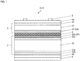
- FIG. 1 is a schematic sectional view showing a configuration of a multi-junction photoelectric conversion device according to one embodiment.
- FIG. 1 is a schematic sectional view of a multi-junction photoelectric conversion device according to one embodiment of the present invention.
- the multi-junction photoelectric conversion device 110 in FIG. 1 includes a light-receiving surface metal electrode 5, light-receiving surface transparent electroconductive layer 14, a first photoelectric conversion unit 1, an intermediate layer 3, a second photoelectric conversion unit 2, a rear surface transparent electroconductive layer 24 and a rear surface metal electrode 6, in this order from the light-receiving side.
- the first photoelectric conversion unit 1 contains a perovskite-type crystal structure photosensitive material as a light absorbing layer 11.
- the second photoelectric conversion unit contains a crystalline silicon substrate as a light absorbing layer 21.
- Crystalline silicon that is used for the light absorbing layer 21 of the second photoelectric conversion unit 2 has a bandgap narrower than that of the perovskite crystal material used for the light absorbing layer 11 of the first photoelectric conversion unit 1.
- the first photoelectric conversion unit 1 is prepared preferably by a wet process. Therefore, it is preferable that the multi-junction photoelectric conversion device 110 shown in FIG. 1 is manufactured by forming the intermediate layer 3 and the first photoelectric conversion unit 1 on the second photoelectric conversion unit 2.
- the second photoelectric conversion unit 2 includes a crystalline silicon substrate as the light absorbing layer 21.
- the crystalline silicon may be either single-crystalline silicon or polycrystalline silicon.
- a single-crystalline silicon substrate is preferably used as the light absorbing layer 21 because it has high long-wavelength light utilization efficiency, and is excellent in carrier recovery efficiency.
- Examples of the photoelectric conversion unit using a single-crystalline silicon substrate include: diffusion-type crystalline silicon photoelectric conversion unit in which an n-type layer is provided on the light-receiving side, and a high-doped region (p+ region) is disposed in rear of a p-type single-crystalline silicon substrate; and heterojunction photoelectric conversion unit in which an amorphous silicon-based thin-film is provided on a p-type or n-type single-crystalline silicon substrate.
- the second photoelectric conversion unit is preferably a heterojunction silicon photoelectric conversion unit from the viewpoint of high conversion efficiency.
- the second photoelectric conversion unit 2 includes a first conductive semiconductor layer as an outermost surface layer 2F on the light-receiving side, which is in contact with the intermediate layer 3.
- the conductive semiconductor layer may be a thin-film formed by a CVD method or the like, or a doped layer with a dopant diffused on a surface of a silicon substrate by means of thermal diffusion or the like.
- the second photoelectric conversion unit 2 is a heterojunction photoelectric conversion unit in which a first conductive silicon-based thin-films 23a is disposed on a light-receiving side of a conductive single-crystalline silicon substrate 21, and a second conductive silicon-based thin-film 23b is disposed on a rear side of the conductive single-crystalline silicon substrate 21.
- One of the conductive silicon-based thin-films 23a and 23b is p-type, and the other is n-type.
- the first conductive silicon-based thin-film 23a is the outermost surface layer 2F on the light-receiving side of the second photoelectric conversion unit 2.
- the conductivity-type of the single-crystalline silicon substrate 21 may be either an n-type or a p-type. In comparison between electron and hole, electron has a higher mobility, and thus when the silicon substrate 21 is an n-type single-crystalline silicon substrate, the conversion characteristic is particularly high.
- the silicon substrate 21 has morphologies on at least one of the light-receiving surface and the rear surface. Morphologies may be formed on a surface of a silicon substrate by, for example, an anisotropic etching. A tetragonal pyramid-shaped morphology is produced by an anisotropic etching.
- a light-receiving surface of the silicon substrate has a morphology, and it is especially preferable that each of surfaces of the silicon substrate has a morphology.
- a morphology such as a texture on a light-receiving surface of the silicon substrate, reflection of light to the first photoelectric conversion unit 1 can be reduced.
- the silicon substrate may have a morphology only on the rear side, and the light-receiving surface of the silicon substrate may be flat and have no morphology.
- the first photoelectric conversion unit 1 When the light-receiving surface of the second photoelectric conversion unit is flat, the first photoelectric conversion unit 1 can be uniformly formed, and generation of pinholes can be reduced.
- the silicon substrate has a morphology on the rear surface, a light confinement effect in long-wavelength range can be expected.
- the height of morphologies on the surface of the silicon substrate 21 is preferably 0.5 ⁇ m or more, more preferably 1 ⁇ m or more.
- the height of the morphologies is preferably 3 ⁇ m or less, more preferably 2 ⁇ m or less.
- the height of morphologies on the surface of the silicon substrate 21 is determined by a height difference between the peak of the projection and the valley of the recess.
- amorphous silicon, microcrystalline silicon (material including amorphous silicon and crystalline silicon), amorphous silicon alloy and microcrystalline silicon alloy may be used.
- the silicon alloy include silicon oxide, silicon carbide, silicon nitride silicon germanium and the like.
- conductive silicon-based thin-film is preferably an amorphous silicon thin-film.
- the photoelectric conversion unit 2 is a heterojunction photoelectric conversion unit
- the photoelectric conversion unit includes intrinsic silicon-based thin-films 22a and 22b between the single-crystalline silicon substrate 21 and the conductive silicon-based thin-films 23a and 23b.
- the intrinsic silicon-based thin-films 22a and 22b are preferably intrinsic amorphous silicon thin-films.
- the above intrinsic silicon-based thin-films 22a and 22b, and conductive silicon-based thin-films 23a and 23b are preferably formed by a plasma-enhanced CVD method.
- the first photoelectric conversion unit 1 includes a first charge transport layer 12, a light absorbing layer 11 and a second charge transport layer 13 in this order from the light-receiving side.
- One of the first charge transport layer 12 and the second charge transport layer 13 is a hole transport layer, and the other is an electron transport layer.
- the second charge transport layer 13 is an outermost surface layer 1R on the rear side in the first photoelectric conversion unit, and is in contact with the intermediate layer 3.
- the first photoelectric conversion unit 1 and the second photoelectric conversion unit 2 are connected in series.
- the outermost surface layer 2F (first conductive silicon layer 53a) disposed on the second photoelectric conversion unit 2 on the intermediate layer 3 is a p-type layer
- the first charge transport layer 12 of the first photoelectric conversion unit 1 is a hole transport layer
- the second charge transport layer 13 is an electron transport layer.
- the first photoelectric conversion unit 1 including the electron transport layer 13, the light absorbing layer 11 and the hole transport layer 12 in this order on the intermediate layer 3 (on the light-receiving side) will be described.
- the electron transport layer 13 As a material of the electron transport layer 13, a known material may be appropriately selected, and examples thereof include titanium oxide, zinc oxide, niobium oxide, zirconium oxide and aluminum oxide.
- the electron transport layer may contain a donor.
- examples of the donor include yttrium, europium and terbium.
- the electron transport layer 13 may be a dense layer having a smooth structure, or a porous layer having a porous structure.
- the pore size is preferably on the nanoscale.
- the electron transport layer preferably has a porous structure for increasing the active surface area of the light absorbing layer 11 to obtain an electron transport layer having an excellent electron collecting ability.
- the electron transport layer may be a single layer, or may have a stacking configuration with a plurality of layers.
- the electron transport layer may have a double layer structure in which a dense layer (compact layer) is arranged on the intermediate layer 3-side, and a porous layer is arranged on the light absorbing layer 11-side.
- the thickness of the electron transport layer is preferably 1 nm to 200 nm.
- the electron transport layer 13 is formed by, for example, a spraying method etc. using a solution containing the electron transporting material such as titanium oxide.
- the light absorbing layer 11 contains a perovskite-type crystal structure photosensitive material (perovskite crystal material).
- the compound that forms the perovskite crystal material is represented by, for example, a general formula of RNH 3 MX 3 or HCH(NH 2 ) 2 MX 3 .
- R is an alkyl group, preferably an alkyl group having 1 to 5 carbon atoms, especially preferably a methyl group.
- M is a divalent metal ion, preferably Pb or Sn.
- X is a halogen, and examples thereof include F, Cl, Br and I. All three Xs may be the same halogen element, or include a plurality of halogens.
- the spectral sensitivity characteristic can be adjusted by changing the type and ratio of the halogen.
- the bandgap of the light absorbing layer 11 in the first photoelectric conversion unit 1 is preferably 1.55 to 1.75 eV, more preferably 1.6 to 1.65 eV for making current matching between the first photoelectric conversion unit 1 and the second photoelectric conversion unit 2.
- the perovskite crystal material is represented by the formula CH 3 NH 3 PbI 3-x Br x
- x is preferably about 0 to 0.85 for ensuring that the bandgap is 1.55 to 1.75 eV
- x is preferably about 0.15 to 0.55 for ensuring that the bandgap is 1.60 to 1.65 eV.
- the light absorbing layer 11 is formed by, for example, a spin coating method etc. using a solution containing the above-mentioned perovskite crystal material.
- a known material may be appropriately selected, and examples thereof include polythiophene derivatives such as poly-3-hexylthiophene (P3HT) and poly(3,4-ethylenedioxythiophene) (PEDOT), fluorene derivatives such as 2,2',7,7'-tetrakis-(N,N-di-p-methoxyphenylamine)-9,9'-spirobifluorene (Spiro-OMeTAD), carbazole derivatives such as polyvinyl carbazole, triphenylamine derivatives, diphenylamine derivatives, polysilane derivatives and polyaniline derivatives.
- the material of the hole transport layer include metal oxides such as MoO 3 , WO 3 and NiO.
- the hole transport layer 12 may be a single layer, or may have a stacking configuration with a plurality of layers.
- the thickness of the hole transport layer is preferably 1 nm to 100 nm.
- the hole transport layer 12 is formed by, for example, a spraying method etc. using a solution containing the above-mentioned hole transporting material
- each layer that forms the first photoelectric conversion unit may be formed by a vapor deposition or the like.
- the multi-junction photoelectric conversion device of the present invention includes the intermediate layer 3 between the first photoelectric conversion unit 1 and the second photoelectric conversion unit 2.
- the intermediate layer 3 may be a single layer or a multilayer.
- the second charge transport layer 13 provided on an outermost surface of the first photoelectric conversion unit on the rear side has a refractive index of, for example, about 2.3 (in the case of titanium oxide).
- the conductive semiconductor layer 23a provided on an outermost surface of the second photoelectric conversion unit on the light-receiving side has a refractive index of about 4.3 (in the case of amorphous silicon).
- the intermediate layer 3 having a specific refractive index and thickness is disposed between the first photoelectric conversion unit 1 and the second photoelectric conversion unit 2, so that the amount of light reaching the second photoelectric conversion unit can be increased to improve the conversion efficiency of the multi-junction photoelectric conversion device.
- the average refractive index n of the intermediate layer 3 satisfies n1 ⁇ n ⁇ n2 where n1 is a refractive index of the second charge transport layer 13 of the first photoelectric conversion unit 1, and n2 is a refractive index of the first conductive semiconductor layer 23a of the second photoelectric conversion unit 2.
- the average refractive index n is preferably ( ⁇ (n1 ⁇ n2) - 0.5) - ( ⁇ (n1 ⁇ n2) + 0.5), more preferably ( ⁇ (n1 ⁇ n2) - 0.4) - ( ⁇ (n1 ⁇ n2) + 0.4), further preferably ( ⁇ (n1 ⁇ n2) - 0.3) - ( ⁇ (n1 ⁇ n2) + 0.3).
- n is preferably 2.0 to 3.5, more preferably 2.3 to 3.4, especially preferably 2.5 to 3.3.
- the refractive index of each layer is a refractive index to light having a wavelength of 600 nm, the refractive index being measured by spectroscopic ellipsometry.
- the average refractive index n is a value obtained in the following manner: the product of the refractive index and the thickness (optical path length) of each layer that forms the intermediate layer 3 is calculated, the products for all the layers are added together, and the resulting value is divided by the total thickness of the intermediate layer.
- the charge transport layer 13 of the perovskite photoelectric conversion unit is a porous layer of mesoporous TiO 2 or the like, a region where a perovskite crystal material and TiO 2 are mixed is present on the light absorbing layer 11 side. Even in this case, the anti-reflection effect of the intermediate layer 3 results mainly from control of the light reflection amount by the refractive index difference at the interface, and therefore the refractive index of TiO 2 present at the interface with the intermediate layer may be defined as the refractive index n1 of the charge transport layer 13.
- the refractive index of an intermediate layer has been controlled to increase the amount of light captured in the top cell and the bottom cell.
- the materials of both the top cell and the bottom cell are silicon, and therefore a light reflecting layer having a low refractive index is provided between the top cell and the bottom cell to increase the amount of light captured in the top cell.
- the intermediate layer 3 has an intermediate refractive index between the refractive index n1 of the rear-side outermost surface layer 1R of the first photoelectric conversion unit 1 and the refractive index n2 of the light-receiving-side outermost surface layer 2F of the second photoelectric conversion unit 2, so that the amount of light reaching the bottom cell can be increased to improve the conversion efficiency of the multi-junction photoelectric conversion device.
- the refractive index n of the intermediate layer is close to the square root ( ⁇ (n1 ⁇ n2)) of the product of n1 and n2.
- the optical thickness nd (product of refractive index n and thickness d) of the intermediate layer is a product of a quarter wavelength and an odd number ((2m-1) ⁇ /4 where m is a natural number)
- the phase difference between reflected light at an interface of the intermediate layer 3 on the first photoelectric conversion unit 1 side and reflected light at an interface of the intermediate layer 3 on the second photoelectric conversion unit 2 side is (2m - 1) ⁇ , so that the former light and the latter light interfere so as to cancel each other.
- reflection of light to the first photoelectric conversion unit 1 can be further reduced to increase the amount of light captured in the second photoelectric conversion unit 2.
- the center wavelength for anti-reflection in the intermediate layer 3 is preferably in a range of 400 to 1200 nm.
- the optical thickness nd of the intermediate layer 3 is preferably 100 to 300 nm, more preferably 125 to 275 nm, further preferably 150 to 250 nm.
- the thickness of the intermediate layer 3 is preferably 40 to 80 nm, more preferably 45 to 75 nm.
- the thickness of the intermediate layer is determined by transmission electron microscope (TEM) observation of a cross-section.
- TEM transmission electron microscope
- the refractive index and the thickness of each of other layers are measured in the same manner as described above.
- the direction perpendicular to the slope of the irregularities is defined to be a thickness direction.
- the material of the intermediate layer 3 is not particularly limited as long as it has the above-mentioned refractive index.
- the intermediate layer 3 has a small light absorption over the wavelength range (mainly 500 to 1200 nm) of light that passes through the first photoelectric conversion unit 1 to reach the second photoelectric conversion unit 2.
- the material of the intermediate layer is preferably a silicon-based material.
- Examples of the silicon-based material having a refractive index in the above-described range include SiOx, SiCx and SiNx.
- the refractive index of such a material can be appropriately changed by adjusting the ratio of constituent atoms.
- the intermediate layer 3 also has a function of capturing carriers (holes and electrons) generated in the two photoelectric conversion units 1, 2, and recombining the carriers. Therefore, it is preferable that the intermediate layer 3 has a certain degree of conductivity. As long as the material of the intermediate layer, such as microcrystalline silicon oxide, has crystals growing towards the thickness direction, it can act as the intermediate layer even when it has a high sheet resistance, since carriers move mainly towards the thickness direction in the intermediate layer 3.
- n-type or p-type microcrystalline SiOx is used as silicon oxide for improving the conductivity of the intermediate layer.
- the microcrystalline SiOx layer can be deposited by a plasma CVD method at a CO 2 /SiH 4 ratio of 1 or more under so-called microcrystal preparation conditions in which for example, SiH 4 , CO 2 and H 2 are used as reaction gases, and the H 2 /SiH 4 ratio is high ( e.g., 10 or more).
- PH 3 a doping gas in addition to the above-mentioned reaction gases.
- B 2 H 6 in place of PH 3 as a doping gas, a p-type microcrystalline SiOx layer can be deposited. Both PH 3 and B 2 H 6 may be used as the doping gas.
- Deposition by plasma CVD may be performed at a power supply frequency of 10 to 100 MHz, a power density of 50 to 500 mW/cm 2 , a pressure of 50 to 1500 Pa and a substrate temperature of 150 to 250°C using, for example, capacitively-coupled parallel plate electrodes.
- a power supply frequency 10 to 100 MHz
- a power density of 50 to 500 mW/cm 2 a pressure of 50 to 1500 Pa
- a substrate temperature of 150 to 250°C using, for example, capacitively-coupled parallel plate electrodes.
- the intermediate layer 3 may be a multilayer film.
- the intermediate layer may be, for example, a composite silicon-based thin-film in which the SiOx layer and an n-type microcrystalline silicon layer are stacked.
- the material that forms each layer is not particularly limited as long as the average refractive index n is in the above-mentioned range.
- the material other than the silicon-based material, which forms the intermediate layer include transparent conductive oxides mainly composed of indium oxide, zinc oxide, tin oxide or the like. Generally, transparent conductive oxide has a refractive index of about 1.9.
- the transparent conductive oxide is stacked with a material having a relatively high refractive index, such as a silicon-based material, when the transparent conductive oxide is used as a material of the intermediate layer.
- a material having a relatively high refractive index such as a silicon-based material
- the intermediate layer is a composite layer having a thin transparent electroconductive layer disposed on a surface of an SiOx layer
- an electrical advantage such as a reduction in contact resistance with the photoelectric conversion unit can be expected.
- a transparent electroconductive layer is disposed on a surface of a silicon-based material layer such as SiOx
- a transparent electroconductive layer may be disposed on either the first photoelectric conversion unit 1-side or the second photoelectric conversion unit 2-side.
- Transparent electroconductive layers may be disposed on both sides of the silicon-based material layer.
- the intermediate layer is a multilayer film
- a high anti-reflection effect can be obtained by setting the average refractive index n and the thickness to the same average refractive index n and thickness as in the above-mentioned single layer, although it is necessary to consider influences of reflection and interference of reflected light at each interface in a strict sense.
- a rear surface transparent electroconductive layer 24 is provided on rear side of the second photoelectric conversion unit.
- a light-receiving surface transparent electroconductive layer 14 is provided on light-receiving side of the first photoelectric conversion unit.
- conductive oxide for example, zinc oxide, indium oxide and tin oxide may be used alone or in complex oxide. From the viewpoints of electroconductivity, optical characteristics and long-term reliability, indium-based oxides including indium oxide are preferable. Among them, those having indium tin oxide (ITO) as a main component are more suitably used.
- ITO indium tin oxide
- a dopant may be added to the transparent electroconductive layer
- metal electrodes are provided on transparent electroconductive layers for effectively extracting photo carriers.
- the metal electrode 5 on the light-receiving side is formed in a predetermined pattern shape.
- the metal electrode 6 on the rear side may be formed in a pattern shape, or formed on the entire surface of the transparent electroconductive layer 24.
- a pattern shape light-receiving surface metal electrode 5 is disposed on the transparent electroconductive layer 14 on the light-receiving side, and a rear surface metal electrode 6 is formed on the entire surface of the rear side transparent electroconductive layer 24.
- Examples of the material of the metal electrodes include silver, copper and aluminum and the like.
- the transparent electroconductive layer and the metal electrode can be formed by a PVD method such as a sputtering method or an ion plating method, a CVD method, a printing method, a plating method, or the like.
- a PVD method such as a sputtering method or an ion plating method is preferable for deposition of a transparent electroconductive layer mainly composed of an indium-based oxide.
- the patterned metal electrode is formed by printing of a conductive paste, a plating method, or the like.
- the second photoelectric conversion unit 2 is a heterojunction photoelectric conversion unit
- the conductive silicon-based thin-film 23a on the light-receiving side is p-type
- the conductive silicon-based thin-film 23b on the rear side is n-type.
- the present invention is not limited to the embodiment shown in FIG. 1 .
- the conductive silicon-based thin-film 23a on the light-receiving side may be n-type
- the conductive silicon-based thin-film 23b on the rear side may be p-type.
- the first charge transport layer 12 on the light-receiving side is an electron transport layer
- the second charge transport layer 13 on the rear side is a hole transport layer.
- the photoelectric conversion device of the present invention is preferably encapsulated by using a encapsulant and modularized when put into practical use. Modularization may be carried out by an appropriate measure. For example, a light-receiving surface metal electrode of a photoelectric conversion device and a rear surface metal electrode of an adjacent photoelectric conversion device are electrically connected through a wiring member to connect adjacent photoelectric conversion devices in series. The photoelectric conversion devices may be connected in parallel. A string with a plurality of photoelectric conversion devices connected through wiring members is encapsulated with encapsulants and glass plates to obtain a photoelectric conversion module.
- the optical effect of the intermediate layer was examined by optical simulation of the multi-junction photoelectric conversion device shown in FIG. 1 .
- an n-type single-crystalline silicon substrate having no surface morphology was used, and each layer was supposed to be flat.
- one-dimensional optical calculation was performed to determine the light absorption ratio in the light absorbing layer of each of the first photoelectric conversion unit (perovskite photoelectric conversion unit) and the second photoelectric conversion unit (heterojunction photoelectric conversion unit), and on the basis of the light absorption ratios, the spectral sensitivity current (Jsc) was calculated.
- the refractive index and the extinction coefficient of each material are values measure by a spectroscopic ellipsometer (trade name: M 2000, manufactured by J. A. Woollam Co., Inc.) using a film formed on a glass plate.
- a value at a wavelength of 600 nm is described as the refractive index n, but in calculation, the refractive index and the extinction coefficient at each wavelength in a range of 300 to 1200 nm were used.
- the layer configuration of the multi-junction photoelectric conversion device in optical simulation was as described below in the order from the light-receiving side.
- the refractive index n and the thickness d of the intermediate layer 3 were changed in the above-mentioned structure, and the current density of the heterojunction photoelectric conversion unit and the current density of the perovskite photoelectric conversion unit were calculated for each refractive index and thickness.
- the rate of change (%) from the current density in the absence of the intermediate layer (when the thickness d of the intermediate layer is 0) was determined.
- the rate of change of the current density of the heterojunction photoelectric conversion unit is shown in Table 1
- the rate of change of the current density of the perovskite photoelectric conversion unit is shown in Table 2.
- Table 3 shows a difference between the current density of the perovskite photoelectric conversion device and the current density of the heterojunction photoelectric conversion device at the refractive index and thickness of each intermediate reflection layer.
Landscapes
- Electromagnetism (AREA)
- Physics & Mathematics (AREA)
- Engineering & Computer Science (AREA)
- Chemical & Material Sciences (AREA)
- Materials Engineering (AREA)
- Power Engineering (AREA)
- Electrochemistry (AREA)
- Chemical Kinetics & Catalysis (AREA)
- Microelectronics & Electronic Packaging (AREA)
- Photovoltaic Devices (AREA)
- Life Sciences & Earth Sciences (AREA)
- Sustainable Development (AREA)
- Sustainable Energy (AREA)
Abstract
Description
- The present invention relates to a multi-junction photoelectric conversion device and a photoelectric conversion module.
- A photoelectric conversion device utilizing an organic metal perovskite-type crystal material (perovskite photoelectric conversion device) can provide a high conversion efficiency, and a large number of reports have recently been published on improvement on conversion efficiency (e.g., Non-Patent
Document 1 and Patent Document 1). Example of the organic metal includes a compound represented by a general formula RNH3MX3 or HC(NH2)2MX3 (where R is an alkyl group, M is a divalent metal ion, and X is a halogen). Spectral sensitivity characteristics of the compound are known to vary depending on the halogen and/or the ratio of the halogen (e.g., Non-Patent Document 2). - A perovskite-type crystal material, such as CH3NH3PbX3 (X: halogen), can be formed by a vapor deposition, spin coating and the like. Especially, a thin-film can be formed in low cost with using a solution coating method such as spin coating. Thus, attention has been directed to a perovskite photoelectric conversion device as a low-cost and high-efficiency next generation photoelectric conversion device.
- For example, a perovskite-type crystal material using iodine as a halogen has a spectral sensitivity characteristic at a wavelength shorter than a wavelength of 800 nm, and absorbs little infrared light having a wavelength longer than 800 nm. Thus, for improvement of the conversion efficiency of a photoelectric conversion device including a perovskite-type crystal material, it is important to effectively utilize long-wavelength light which is absorbed only in a small amount by the perovskite-type crystal material.
- For example, Non-Patent
Document 3 discloses a double-junction solar cell in which on a crystalline silicon photoelectric conversion unit including a p-type emitter layer on a light-receiving side surface of an n-type single-crystalline silicon substrate, a perovskite photoelectric conversion unit is provided with an n-type tunnel junction layer and a TiO2 layer interposed therebetween, and a crystalline silicon photoelectric conversion unit and a perovskite photoelectric conversion unit are connected in series. - Patent Document 1:
JP 2014-72327 A -
- Non Patent Document 1: G. Hodes, Science, 342, 317-318 (2013).
- Non Patent Document 2: A. Kojima et. al., J. Am. Chem. Soc., 131, 6050-6051 (2009).
- Non Patent Document 3: J. P. Mailoa et al., APPLIED PHYSICS LETTERS 106, 121105 (2015)
- Non-Patent
Document 3 suggests that by providing an n-type silicon tunnel junction layer between a p-type silicon emitter layer that forms a crystalline silicon photoelectric conversion unit and a TiO2 layer that forms a perovskite photoelectric conversion unit, a favorable electrical junction is formed between the two photoelectric conversion units. On the other hand, the double-junction solar cell inNon-Patent Document 3 has a low short-circuit current density Jsc, and cannot sufficiently exhibit the effect of improving light utilization efficiency by multi-junction. - In view of the situations described above, an object of the present invention is to provide a high-efficiency photoelectric conversion device in which a perovskite photoelectric conversion unit is combined with a crystalline silicon-based photoelectric conversion unit.
- The present inventors have extensively conducted studies in view of the above-mentioned problems, and resultantly found that by providing a specific intermediate layer between a perovskite photoelectric conversion unit and a crystalline silicon-based photoelectric conversion unit, the conversion efficiency of a multi-junction photoelectric conversion device can be improved.
- A multi-junction photoelectric conversion device of the present invention includes a first photoelectric conversion unit, an intermediate layer and a second photoelectric conversion unit in this order from the light-receiving side. The first photoelectric conversion unit contains a perovskite-type crystal structure photosensitive material as a light absorbing layer, and includes a first charge transport layer on the light-receiving side of the light absorbing layer, and a second charge transport layer on the rear side of the light absorbing layer. The second charge transport layer is in contact with the intermediate layer. The second photoelectric conversion unit includes a crystalline silicon substrate as a light absorbing layer, and a first conductive semiconductor layer that is in contact with the intermediate layer.
- A refractive index n1 of the second charge transport layer, a refractive index n2 of the first conductive semiconductor layer, and an average refractive index n of the intermediate layer satisfy the relationships of n1 < n < n2, n2 - n1 ≥ 0.7 and √(n1 × n2) - 0.5 ≤ n ≤ √(n1 × n2) + 0.5. The average refractive index n of the intermediate layer is preferably 2.0 to 3.5. The thickness of the intermediate layer is preferably 40 to 80 nm. The product of the average refractive index of the intermediate layer and the thickness is preferably 100 to 300 nm.
- The balance of the photocurrents of the photoelectric conversion units can be adjusted by providing a specific intermediate layer between a perovskite photoelectric conversion unit and a crystalline silicon-based photoelectric conversion unit, so that the efficiency of a multi-junction photoelectric conversion device can be improved.
-
FIG. 1 is a schematic sectional view showing a configuration of a multi-junction photoelectric conversion device according to one embodiment. -
FIG. 1 is a schematic sectional view of a multi-junction photoelectric conversion device according to one embodiment of the present invention. The multi-junctionphotoelectric conversion device 110 inFIG. 1 includes a light-receivingsurface metal electrode 5, light-receiving surface transparentelectroconductive layer 14, a firstphotoelectric conversion unit 1, anintermediate layer 3, a secondphotoelectric conversion unit 2, a rear surface transparentelectroconductive layer 24 and a rearsurface metal electrode 6, in this order from the light-receiving side. The firstphotoelectric conversion unit 1 contains a perovskite-type crystal structure photosensitive material as alight absorbing layer 11. The second photoelectric conversion unit contains a crystalline silicon substrate as alight absorbing layer 21. - Crystalline silicon that is used for the
light absorbing layer 21 of the secondphotoelectric conversion unit 2 has a bandgap narrower than that of the perovskite crystal material used for thelight absorbing layer 11 of the firstphotoelectric conversion unit 1. By disposing the second photoelectric conversion unit having a narrow bandgap on the rear side of the first photoelectric conversion unit, long-wavelength light, which is not absorbed by the first photoelectric conversion unit, of light incident from the light-receiving surface (first photoelectric conversion unit side), can be utilized in the second photoelectric conversion unit, and therefore a multi-junction photoelectric conversion device with an excellent light utilization efficiency can be obtained. - The first
photoelectric conversion unit 1 is prepared preferably by a wet process. Therefore, it is preferable that the multi-junctionphotoelectric conversion device 110 shown inFIG. 1 is manufactured by forming theintermediate layer 3 and the firstphotoelectric conversion unit 1 on the secondphotoelectric conversion unit 2. - The second
photoelectric conversion unit 2 includes a crystalline silicon substrate as thelight absorbing layer 21. The crystalline silicon may be either single-crystalline silicon or polycrystalline silicon. In particular, a single-crystalline silicon substrate is preferably used as thelight absorbing layer 21 because it has high long-wavelength light utilization efficiency, and is excellent in carrier recovery efficiency. - Examples of the photoelectric conversion unit using a single-crystalline silicon substrate include: diffusion-type crystalline silicon photoelectric conversion unit in which an n-type layer is provided on the light-receiving side, and a high-doped region (p+ region) is disposed in rear of a p-type single-crystalline silicon substrate; and heterojunction photoelectric conversion unit in which an amorphous silicon-based thin-film is provided on a p-type or n-type single-crystalline silicon substrate. In particular, the second photoelectric conversion unit is preferably a heterojunction silicon photoelectric conversion unit from the viewpoint of high conversion efficiency.
- The second
photoelectric conversion unit 2 includes a first conductive semiconductor layer as anoutermost surface layer 2F on the light-receiving side, which is in contact with theintermediate layer 3. The conductive semiconductor layer may be a thin-film formed by a CVD method or the like, or a doped layer with a dopant diffused on a surface of a silicon substrate by means of thermal diffusion or the like. - In the multi-junction photoelectric conversion device shown in
FIG. 1 , the secondphotoelectric conversion unit 2 is a heterojunction photoelectric conversion unit in which a first conductive silicon-based thin-films 23a is disposed on a light-receiving side of a conductive single-crystalline silicon substrate 21, and a second conductive silicon-based thin-film 23b is disposed on a rear side of the conductive single-crystalline silicon substrate 21. One of the conductive silicon-based thin-films film 23a is theoutermost surface layer 2F on the light-receiving side of the secondphotoelectric conversion unit 2. - The conductivity-type of the single-
crystalline silicon substrate 21 may be either an n-type or a p-type. In comparison between electron and hole, electron has a higher mobility, and thus when thesilicon substrate 21 is an n-type single-crystalline silicon substrate, the conversion characteristic is particularly high. - Preferably, the
silicon substrate 21 has morphologies on at least one of the light-receiving surface and the rear surface. Morphologies may be formed on a surface of a silicon substrate by, for example, an anisotropic etching. A tetragonal pyramid-shaped morphology is produced by an anisotropic etching. - From the viewpoint of light incidence, it is preferable that a light-receiving surface of the silicon substrate has a morphology, and it is especially preferable that each of surfaces of the silicon substrate has a morphology. By forming a morphology such as a texture on a light-receiving surface of the silicon substrate, reflection of light to the first
photoelectric conversion unit 1 can be reduced. When the firstphotoelectric conversion unit 1 is formed by a wet process, the silicon substrate may have a morphology only on the rear side, and the light-receiving surface of the silicon substrate may be flat and have no morphology. When the light-receiving surface of the second photoelectric conversion unit is flat, the firstphotoelectric conversion unit 1 can be uniformly formed, and generation of pinholes can be reduced. When the silicon substrate has a morphology on the rear surface, a light confinement effect in long-wavelength range can be expected. - The height of morphologies on the surface of the
silicon substrate 21 is preferably 0.5 µm or more, more preferably 1 µm or more. The height of the morphologies is preferably 3 µm or less, more preferably 2 µm or less. When the height of morphologies is in the above-mentioned range, the reflectance of a surface of the substrate can be reduced to increase a short circuit current. The height of morphologies on the surface of thesilicon substrate 21 is determined by a height difference between the peak of the projection and the valley of the recess. - As the conductive silicon-based thin-
films - When the second
photoelectric conversion unit 2 is a heterojunction photoelectric conversion unit, it is preferable that the photoelectric conversion unit includes intrinsic silicon-based thin-films crystalline silicon substrate 21 and the conductive silicon-based thin-films crystalline silicon substrate 21, the intrinsic silicon-based thin-films - The above intrinsic silicon-based thin-
films films - An
intermediate layer 3 is deposited on the secondphotoelectric conversion unit 2, and a firstphotoelectric conversion unit 1 is deposited on theintermediate layer 3. The firstphotoelectric conversion unit 1 includes a firstcharge transport layer 12, alight absorbing layer 11 and a secondcharge transport layer 13 in this order from the light-receiving side. One of the firstcharge transport layer 12 and the secondcharge transport layer 13 is a hole transport layer, and the other is an electron transport layer. The secondcharge transport layer 13 is anoutermost surface layer 1R on the rear side in the first photoelectric conversion unit, and is in contact with theintermediate layer 3. - The first
photoelectric conversion unit 1 and the secondphotoelectric conversion unit 2 are connected in series. Thus, when theoutermost surface layer 2F (first conductive silicon layer 53a) disposed on the secondphotoelectric conversion unit 2 on theintermediate layer 3 is a p-type layer, the firstcharge transport layer 12 of the firstphotoelectric conversion unit 1 is a hole transport layer, and the secondcharge transport layer 13 is an electron transport layer. - Hereinafter, a configuration of the first
photoelectric conversion unit 1 including theelectron transport layer 13, thelight absorbing layer 11 and thehole transport layer 12 in this order on the intermediate layer 3 (on the light-receiving side) will be described. - As a material of the
electron transport layer 13, a known material may be appropriately selected, and examples thereof include titanium oxide, zinc oxide, niobium oxide, zirconium oxide and aluminum oxide. The electron transport layer may contain a donor. For example, when titanium oxide is used for the electron transport layer, examples of the donor include yttrium, europium and terbium. - The
electron transport layer 13 may be a dense layer having a smooth structure, or a porous layer having a porous structure. When the electron transport layer has a porous structure, the pore size is preferably on the nanoscale. The electron transport layer preferably has a porous structure for increasing the active surface area of thelight absorbing layer 11 to obtain an electron transport layer having an excellent electron collecting ability. - The electron transport layer may be a single layer, or may have a stacking configuration with a plurality of layers. For example, the electron transport layer may have a double layer structure in which a dense layer (compact layer) is arranged on the intermediate layer 3-side, and a porous layer is arranged on the light absorbing layer 11-side. The thickness of the electron transport layer is preferably 1 nm to 200 nm.
- The
electron transport layer 13 is formed by, for example, a spraying method etc. using a solution containing the electron transporting material such as titanium oxide. - The
light absorbing layer 11 contains a perovskite-type crystal structure photosensitive material (perovskite crystal material). The compound that forms the perovskite crystal material is represented by, for example, a general formula of RNH3MX3 or HCH(NH2)2MX3. In the formula, R is an alkyl group, preferably an alkyl group having 1 to 5 carbon atoms, especially preferably a methyl group. M is a divalent metal ion, preferably Pb or Sn. X is a halogen, and examples thereof include F, Cl, Br and I. All three Xs may be the same halogen element, or include a plurality of halogens. The spectral sensitivity characteristic can be adjusted by changing the type and ratio of the halogen. - The bandgap of the
light absorbing layer 11 in the firstphotoelectric conversion unit 1 is preferably 1.55 to 1.75 eV, more preferably 1.6 to 1.65 eV for making current matching between the firstphotoelectric conversion unit 1 and the secondphotoelectric conversion unit 2. For example, when the perovskite crystal material is represented by the formula CH3NH3PbI3-xBrx, x is preferably about 0 to 0.85 for ensuring that the bandgap is 1.55 to 1.75 eV, and x is preferably about 0.15 to 0.55 for ensuring that the bandgap is 1.60 to 1.65 eV. - The
light absorbing layer 11 is formed by, for example, a spin coating method etc. using a solution containing the above-mentioned perovskite crystal material. - As a material of the
hole transport layer 12, a known material may be appropriately selected, and examples thereof include polythiophene derivatives such as poly-3-hexylthiophene (P3HT) and poly(3,4-ethylenedioxythiophene) (PEDOT), fluorene derivatives such as 2,2',7,7'-tetrakis-(N,N-di-p-methoxyphenylamine)-9,9'-spirobifluorene (Spiro-OMeTAD), carbazole derivatives such as polyvinyl carbazole, triphenylamine derivatives, diphenylamine derivatives, polysilane derivatives and polyaniline derivatives. Examples of the material of the hole transport layer include metal oxides such as MoO3, WO3 and NiO. - The
hole transport layer 12 may be a single layer, or may have a stacking configuration with a plurality of layers. The thickness of the hole transport layer is preferably 1 nm to 100 nm. Thehole transport layer 12 is formed by, for example, a spraying method etc. using a solution containing the above-mentioned hole transporting material - The configuration of the first
photoelectric conversion unit 1 and the method for formation thereof are not limited to those described above. For example, each layer that forms the first photoelectric conversion unit may be formed by a vapor deposition or the like. - The multi-junction photoelectric conversion device of the present invention includes the
intermediate layer 3 between the firstphotoelectric conversion unit 1 and the secondphotoelectric conversion unit 2. Theintermediate layer 3 may be a single layer or a multilayer. - The second
charge transport layer 13 provided on an outermost surface of the first photoelectric conversion unit on the rear side has a refractive index of, for example, about 2.3 (in the case of titanium oxide). Theconductive semiconductor layer 23a provided on an outermost surface of the second photoelectric conversion unit on the light-receiving side has a refractive index of about 4.3 (in the case of amorphous silicon). When the second charge transport layer of the first photoelectric conversion unit and the first conductive semiconductor layer of the second photoelectric conversion unit are in direct contact with each other, the refractive index difference at the interface of the photoelectric conversion units is large. In particular, when a difference (n2 - n1) between the refractive index n1 of the second charge transport layer of the firstphotoelectric conversion unit 1 and the refractive index n2 of the firstconductive semiconductor layer 23a of the secondphotoelectric conversion unit 2 is 0.7 or more, the reflection loss caused by the refractive index difference markedly increases. - In the present invention, the
intermediate layer 3 having a specific refractive index and thickness is disposed between the firstphotoelectric conversion unit 1 and the secondphotoelectric conversion unit 2, so that the amount of light reaching the second photoelectric conversion unit can be increased to improve the conversion efficiency of the multi-junction photoelectric conversion device. - The average refractive index n of the
intermediate layer 3 satisfies n1 < n < n2 where n1 is a refractive index of the secondcharge transport layer 13 of the firstphotoelectric conversion unit 1, and n2 is a refractive index of the firstconductive semiconductor layer 23a of the secondphotoelectric conversion unit 2. The average refractive index n is preferably (√(n1 × n2) - 0.5) - (√(n1 × n2) + 0.5), more preferably (√(n1 × n2) - 0.4) - (√(n1 × n2) + 0.4), further preferably (√(n1 × n2) - 0.3) - (√(n1 × n2) + 0.3). n is preferably 2.0 to 3.5, more preferably 2.3 to 3.4, especially preferably 2.5 to 3.3. - The refractive index of each layer is a refractive index to light having a wavelength of 600 nm, the refractive index being measured by spectroscopic ellipsometry. When the intermediate layer is a multilayer, the average refractive index n is a value obtained in the following manner: the product of the refractive index and the thickness (optical path length) of each layer that forms the
intermediate layer 3 is calculated, the products for all the layers are added together, and the resulting value is divided by the total thickness of the intermediate layer. When thecharge transport layer 13 of the perovskite photoelectric conversion unit is a porous layer of mesoporous TiO2 or the like, a region where a perovskite crystal material and TiO2 are mixed is present on thelight absorbing layer 11 side. Even in this case, the anti-reflection effect of theintermediate layer 3 results mainly from control of the light reflection amount by the refractive index difference at the interface, and therefore the refractive index of TiO2 present at the interface with the intermediate layer may be defined as the refractive index n1 of thecharge transport layer 13. - Heretofore, in a thin-film silicon-based multi-junction photoelectric conversion device in which an amorphous silicon thin-film photoelectric conversion unit (top cell) on the light-receiving side and a microcrystalline silicon thin-film photoelectric conversion unit (bottom cell) on the rear side are stacked, the refractive index of an intermediate layer has been controlled to increase the amount of light captured in the top cell and the bottom cell. In the thin-film silicon-based multi-junction photoelectric conversion device, the materials of both the top cell and the bottom cell are silicon, and therefore a light reflecting layer having a low refractive index is provided between the top cell and the bottom cell to increase the amount of light captured in the top cell.
- On the other hand, it has been found that when a perovskite photoelectric conversion unit and a crystalline silicon-based photoelectric conversion unit are stacked, light is easily reflected at the junction interface because the refractive index difference between the units is large, and thus the amount of light captured in the crystalline silicon-based photoelectric conversion unit disposed on the rear side is small, so that deterioration of light utilization efficiency, and imbalance of currents between the top cell and the bottom cell easily occur. In the present invention, on the basis of an optical design concept opposite to that for the intermediate layer in a conventional multi-junction solar cell using thin-film silicon, the
intermediate layer 3 has an intermediate refractive index between the refractive index n1 of the rear-sideoutermost surface layer 1R of the firstphotoelectric conversion unit 1 and the refractive index n2 of the light-receiving-sideoutermost surface layer 2F of the secondphotoelectric conversion unit 2, so that the amount of light reaching the bottom cell can be increased to improve the conversion efficiency of the multi-junction photoelectric conversion device. - For obtaining the anti-reflection effect of the
intermediate layer 3, it is preferable that the refractive index n of the intermediate layer is close to the square root (√(n1 × n2)) of the product of n1 and n2. Further, when the optical thickness nd (product of refractive index n and thickness d) of the intermediate layer is a product of a quarter wavelength and an odd number ((2m-1) λ/4 where m is a natural number), the phase difference between reflected light at an interface of theintermediate layer 3 on the firstphotoelectric conversion unit 1 side and reflected light at an interface of theintermediate layer 3 on the secondphotoelectric conversion unit 2 side is (2m - 1)π, so that the former light and the latter light interfere so as to cancel each other. Thus, reflection of light to the firstphotoelectric conversion unit 1 can be further reduced to increase the amount of light captured in the secondphotoelectric conversion unit 2. - For matching the photocurrent amount of the first photoelectric conversion unit with the photocurrent amount of the second photoelectric conversion unit, the center wavelength for anti-reflection in the
intermediate layer 3 is preferably in a range of 400 to 1200 nm. Thus, the optical thickness nd of theintermediate layer 3 is preferably 100 to 300 nm, more preferably 125 to 275 nm, further preferably 150 to 250 nm. The thickness of theintermediate layer 3 is preferably 40 to 80 nm, more preferably 45 to 75 nm. - The thickness of the intermediate layer is determined by transmission electron microscope (TEM) observation of a cross-section. The refractive index and the thickness of each of other layers are measured in the same manner as described above. When a thin-film is formed on a silicon substrate having morphologies, the direction perpendicular to the slope of the irregularities is defined to be a thickness direction.
- The material of the
intermediate layer 3 is not particularly limited as long as it has the above-mentioned refractive index. Preferably, theintermediate layer 3 has a small light absorption over the wavelength range (mainly 500 to 1200 nm) of light that passes through the firstphotoelectric conversion unit 1 to reach the secondphotoelectric conversion unit 2. The material of the intermediate layer is preferably a silicon-based material. - Examples of the silicon-based material having a refractive index in the above-described range include SiOx, SiCx and SiNx. The refractive index of such a material can be appropriately changed by adjusting the ratio of constituent atoms. In particular, it is preferable to use silicon oxide (SiOx) from the viewpoint of high permeability and high conductivity.
- The
intermediate layer 3 also has a function of capturing carriers (holes and electrons) generated in the twophotoelectric conversion units intermediate layer 3 has a certain degree of conductivity. As long as the material of the intermediate layer, such as microcrystalline silicon oxide, has crystals growing towards the thickness direction, it can act as the intermediate layer even when it has a high sheet resistance, since carriers move mainly towards the thickness direction in theintermediate layer 3. Preferably, n-type or p-type microcrystalline SiOx is used as silicon oxide for improving the conductivity of the intermediate layer. - The microcrystalline SiOx layer can be deposited by a plasma CVD method at a CO2/SiH4 ratio of 1 or more under so-called microcrystal preparation conditions in which for example, SiH4, CO2 and H2 are used as reaction gases, and the H2/SiH4 ratio is high (e.g., 10 or more). When the n-type microcrystalline SiOx layer is deposited, it is preferable to use PH3 as a doping gas in addition to the above-mentioned reaction gases. By using B2H6 in place of PH3 as a doping gas, a p-type microcrystalline SiOx layer can be deposited. Both PH3 and B2H6 may be used as the doping gas. Deposition by plasma CVD may be performed at a power supply frequency of 10 to 100 MHz, a power density of 50 to 500 mW/cm2, a pressure of 50 to 1500 Pa and a substrate temperature of 150 to 250°C using, for example, capacitively-coupled parallel plate electrodes. When the CO2/SiH4 ratio is reduced, the oxygen concentration in the film decreases, so the refractive index can be controlled. By such a deposition method, an SiOx intermediate layer having a desired refractive index and light transmittance and conductivity can be formed.
- The
intermediate layer 3 may be a multilayer film. The intermediate layer may be, for example, a composite silicon-based thin-film in which the SiOx layer and an n-type microcrystalline silicon layer are stacked. When the intermediate layer includes a plurality of layers, the material that forms each layer is not particularly limited as long as the average refractive index n is in the above-mentioned range. Examples of the material other than the silicon-based material, which forms the intermediate layer, include transparent conductive oxides mainly composed of indium oxide, zinc oxide, tin oxide or the like. Generally, transparent conductive oxide has a refractive index of about 1.9. Therefore, it is preferable that the transparent conductive oxide is stacked with a material having a relatively high refractive index, such as a silicon-based material, when the transparent conductive oxide is used as a material of the intermediate layer. For example, when the intermediate layer is a composite layer having a thin transparent electroconductive layer disposed on a surface of an SiOx layer, an electrical advantage such as a reduction in contact resistance with the photoelectric conversion unit can be expected. When a transparent electroconductive layer is disposed on a surface of a silicon-based material layer such as SiOx, a transparent electroconductive layer may be disposed on either the first photoelectric conversion unit 1-side or the second photoelectric conversion unit 2-side. Transparent electroconductive layers may be disposed on both sides of the silicon-based material layer. When the intermediate layer is a multilayer film, a high anti-reflection effect can be obtained by setting the average refractive index n and the thickness to the same average refractive index n and thickness as in the above-mentioned single layer, although it is necessary to consider influences of reflection and interference of reflected light at each interface in a strict sense. - Preferably, a rear surface
transparent electroconductive layer 24 is provided on rear side of the second photoelectric conversion unit. Preferably, a light-receiving surfacetransparent electroconductive layer 14 is provided on light-receiving side of the first photoelectric conversion unit. As a material of the transparent electroconductive layers, conductive oxide, for example, zinc oxide, indium oxide and tin oxide may be used alone or in complex oxide. From the viewpoints of electroconductivity, optical characteristics and long-term reliability, indium-based oxides including indium oxide are preferable. Among them, those having indium tin oxide (ITO) as a main component are more suitably used. A dopant may be added to the transparent electroconductive layer - Preferably, metal electrodes are provided on transparent electroconductive layers for effectively extracting photo carriers. The
metal electrode 5 on the light-receiving side is formed in a predetermined pattern shape. Themetal electrode 6 on the rear side may be formed in a pattern shape, or formed on the entire surface of thetransparent electroconductive layer 24. In the embodiment shown inFIG. 1 , a pattern shape light-receivingsurface metal electrode 5 is disposed on thetransparent electroconductive layer 14 on the light-receiving side, and a rearsurface metal electrode 6 is formed on the entire surface of the rear sidetransparent electroconductive layer 24. Examples of the material of the metal electrodes include silver, copper and aluminum and the like. - The transparent electroconductive layer and the metal electrode can be formed by a PVD method such as a sputtering method or an ion plating method, a CVD method, a printing method, a plating method, or the like. A PVD method such as a sputtering method or an ion plating method is preferable for deposition of a transparent electroconductive layer mainly composed of an indium-based oxide. The patterned metal electrode is formed by printing of a conductive paste, a plating method, or the like.
- An example has been described in which the second
photoelectric conversion unit 2 is a heterojunction photoelectric conversion unit, the conductive silicon-based thin-film 23a on the light-receiving side is p-type, and the conductive silicon-based thin-film 23b on the rear side is n-type. The present invention is not limited to the embodiment shown inFIG. 1 . For example, in the secondphotoelectric conversion unit 2, the conductive silicon-based thin-film 23a on the light-receiving side may be n-type, and the conductive silicon-based thin-film 23b on the rear side may be p-type. In this case, in the firstphotoelectric conversion unit 1, the firstcharge transport layer 12 on the light-receiving side is an electron transport layer, and the secondcharge transport layer 13 on the rear side is a hole transport layer. - The photoelectric conversion device of the present invention is preferably encapsulated by using a encapsulant and modularized when put into practical use. Modularization may be carried out by an appropriate measure. For example, a light-receiving surface metal electrode of a photoelectric conversion device and a rear surface metal electrode of an adjacent photoelectric conversion device are electrically connected through a wiring member to connect adjacent photoelectric conversion devices in series. The photoelectric conversion devices may be connected in parallel. A string with a plurality of photoelectric conversion devices connected through wiring members is encapsulated with encapsulants and glass plates to obtain a photoelectric conversion module.
- The optical effect of the intermediate layer was examined by optical simulation of the multi-junction photoelectric conversion device shown in
FIG. 1 . In this example, an n-type single-crystalline silicon substrate having no surface morphology was used, and each layer was supposed to be flat. In optical simulation, using the refractive index and the extinction coefficient of each layer, one-dimensional optical calculation was performed to determine the light absorption ratio in the light absorbing layer of each of the first photoelectric conversion unit (perovskite photoelectric conversion unit) and the second photoelectric conversion unit (heterojunction photoelectric conversion unit), and on the basis of the light absorption ratios, the spectral sensitivity current (Jsc) was calculated. - As optical simulation software, "SunShine" from Ljubljana University was used. The refractive index and the extinction coefficient of each material are values measure by a spectroscopic ellipsometer (trade name: M 2000, manufactured by J. A. Woollam Co., Inc.) using a film formed on a glass plate. Hereinafter, a value at a wavelength of 600 nm is described as the refractive index n, but in calculation, the refractive index and the extinction coefficient at each wavelength in a range of 300 to 1200 nm were used.
- The layer configuration of the multi-junction photoelectric conversion device in optical simulation was as described below in the order from the light-receiving side.
- Anti-reflection film: MgF2 (refractive index = 1.4, thickness = 100nm)
- ITO (refractive index = 2.0, thickness = 60nm)
-
- Hole transport layer: Spiro-OMeTAD (refractive index = 1.8, thickness = 50nm)
- Light absorbing layer: CH3NH3PbI3 (refractive index = 2.3, thickness = 200nm)
- Electron transport layer: TiO2 (refractive index = 1.5, thickness = 10nm); and TiO2 compact layer (refractive indexn1 = 2.3, thickness = 50nm)
- n-type microcrystalline SiOx layer (refractive index n = 2.0 to 4.0, thickness d = 10 to 100nm)
-
- p-type amorphous silicon thin-film (refractive index n2 = 4.3, thickness = 5nm)
- Intrinsic amorphous silicon thin-film (refractive index = 4.2, thickness = 5nm)
- n-type single-crystalline silicon substrate (refractive index = 3.9, thickness = 180µm)
- Intrinsic amorphous silicon thin-film (refractive index = 4.2, thickness = 5nm)
- n-type amorphous silicon thin-film (refractive index = 4.3, thickness = 10nm)
- ITO (refractive index = 2.0, thickness = 50nm)
- The refractive index n and the thickness d of the
intermediate layer 3 were changed in the above-mentioned structure, and the current density of the heterojunction photoelectric conversion unit and the current density of the perovskite photoelectric conversion unit were calculated for each refractive index and thickness. The rate of change (%) from the current density in the absence of the intermediate layer (when the thickness d of the intermediate layer is 0) was determined. The rate of change of the current density of the heterojunction photoelectric conversion unit is shown in Table 1, and the rate of change of the current density of the perovskite photoelectric conversion unit is shown in Table 2.


- In Table 1, mainly in a part surrounded by a solid frame, the current density of the heterojunction photoelectric conversion unit increased as compared to the case where the
intermediate layer 3 was not provided. On the other hand, in Table 2, mainly in a part surrounded by a solid frame, the current density of the perovskite photoelectric conversion unit decreased as compared to the case where theintermediate layer 3 was not provided. These results show that by adjusting the refractive index n and the thickness d of the intermediate layer, reflection of light to the perovskite photoelectric conversion unit-side is reduced, so that the amount of light captured in the heterojunction photoelectric conversion unit increases. - Table 3 shows a difference between the current density of the perovskite photoelectric conversion device and the current density of the heterojunction photoelectric conversion device at the refractive index and thickness of each intermediate reflection layer.

- The results shown in Table 3 suggest that by adjusting the thickness and the refractive index of the intermediate layer, the difference in current density between the perovskite photoelectric conversion unit and the heterojunction photoelectric conversion unit is decreased to improve current matching, so that energy can be efficiently extracted.
-
- 1, 2
- photoelectric conversion unit
- 11
- light absorbing layer (perovskite crystal material layer)
- 12, 13
- charge transport layer
- 21
- light absorbing layer (crystalline silicon substrate)
- 22a, 22b
- intrinsic silicon-based thin-film
- 23a, 23b
- conductive silicon-based thin-film
- 3
- intermediate layer
- 14, 24
- transparent electroconductive layer
- 5, 6
- metal electrode
- 110
- multi-junction photoelectric conversion device
Claims (11)
- A multi-junction photoelectric conversion device comprising:a first photoelectric conversion unit containing a perovskite-type crystal structure photosensitive material as a light absorbing layer;an intermediate layer; anda second photoelectric conversion unit including a crystalline silicon substrate as a light absorbing layer, in this order from a light-receiving side,wherein the first photoelectric conversion unit includes a first charge transport layer on the light-receiving side of the light absorbing layer, and a second charge transport layer on a rear side of the light absorbing layer,the second charge transport layer is in contact with the intermediate layer,the second photoelectric conversion unit includes a first conductive semiconductor layer that is in contact with the intermediate layer, anda refractive index n1 of the second charge transport layer, a refractive index n2 of the first conductive semiconductor layer and an average refractive index n of the intermediate layer satisfy the following relationships:


- The multi-junction photoelectric conversion device according to claim 1, wherein the average refractive index n of the intermediate layer is 2.0 to 3.5.
- The multi-junction photoelectric conversion device according to claim 1 or 2, wherein a thickness of the intermediate layer is 40 to 80 nm.
- The multi-junction photoelectric conversion device according to any one of claims 1 to 3, wherein a product of the average refractive index and a thickness of the intermediate layer is 100 to 300 nm.
- The multi-junction photoelectric conversion device according to any one of claims 1 to 4, wherein the first conductive semiconductor layer is a conductive silicon-based thin-film.
- The multi-junction photoelectric conversion device according to any one of claims 1 to 5, wherein the intermediate layer includes a silicon oxide layer.
- The multi-junction photoelectric conversion device according to claim 6, wherein the intermediate layer includes a microcrystalline silicon oxide layer.
- The multi-junction photoelectric conversion device according to any one of claims 1 to 7, wherein the intermediate layer is consisting of a single layer.
- The multi-junction photoelectric conversion device according to any one of claims 1 to 8, wherein the first charge transport layer is a hole transport layer, and the second charge transport layer is an electron transport layer.
- The multi-junction photoelectric conversion device according to any one of claims 1 to 9, wherein the second photoelectric conversion unit includes a second conductive semiconductor layer having a conductivity type different from that of the first conductive semiconductor layer on the rear side of the crystalline silicon substrate.
- A photoelectric conversion module including the multi-junction photoelectric conversion device according to any one of claims 1 to 10.
Applications Claiming Priority (2)
| Application Number | Priority Date | Filing Date | Title |
|---|---|---|---|
| JP2015194415 | 2015-09-30 | ||
| PCT/JP2016/078953 WO2017057646A1 (en) | 2015-09-30 | 2016-09-29 | Multi-junction photoelectric conversion device and photoelectric conversion module |
Publications (2)
| Publication Number | Publication Date |
|---|---|
| EP3358637A1 true EP3358637A1 (en) | 2018-08-08 |
| EP3358637A4 EP3358637A4 (en) | 2019-06-19 |
Family
ID=58423971
Family Applications (1)
| Application Number | Title | Priority Date | Filing Date |
|---|---|---|---|
| EP16851817.3A Pending EP3358637A4 (en) | 2015-09-30 | 2016-09-29 | MULTI-JUNCTION PHOTOELECTRIC CONVERSION DEVICE AND PHOTOELECTRIC CONVERSION MODULE |
Country Status (5)
| Country | Link |
|---|---|
| US (1) | US10333016B2 (en) |
| EP (1) | EP3358637A4 (en) |
| JP (1) | JP6650462B2 (en) |
| CN (1) | CN108140735B (en) |
| WO (1) | WO2017057646A1 (en) |
Cited By (1)
| Publication number | Priority date | Publication date | Assignee | Title |
|---|---|---|---|---|
| US12347630B2 (en) | 2022-03-18 | 2025-07-01 | Kabushiki Kaisha Toshiba | Multilayer junction photoelectric converter and method for manufacturing multilayer junction photoelectric converter |
Families Citing this family (25)
| Publication number | Priority date | Publication date | Assignee | Title |
|---|---|---|---|---|
| EP3457448B1 (en) * | 2016-05-09 | 2022-06-15 | Kaneka Corporation | Stacked photoelectric conversion device and method for producing same |
| JP6986418B2 (en) * | 2017-11-07 | 2021-12-22 | 株式会社カネカ | Manufacturing method of laminated photoelectric conversion device and laminated photoelectric conversion device module |
| KR102086809B1 (en) * | 2018-05-23 | 2020-03-06 | 한국과학기술연구원 | Tandem solar cells with transparent conducting electrode with high refractive index |
| US12433148B2 (en) | 2018-09-27 | 2025-09-30 | Alliance For Sustainable Energy, Llc | Optoelectronic devices and methods of making the same |
| WO2020072314A2 (en) | 2018-09-27 | 2020-04-09 | Alliance For Sustainable Energy, Llc | Optoelectronic devices and methods of making the same |
| EP3660927B1 (en) * | 2018-11-30 | 2021-11-10 | CSEM Centre Suisse D'electronique Et De Microtechnique SA | Photovoltaic module |
| GB201820427D0 (en) * | 2018-12-14 | 2019-01-30 | Univ Oxford Innovation Ltd | Device interlayer |
| SG11202107556SA (en) * | 2019-01-16 | 2021-08-30 | Univ Michigan Regents | Photodetectors with semiconductor active layers for under-display fingerprint and gesture sensors |
| DE102019113343B4 (en) * | 2019-05-20 | 2025-12-31 | Senorics Gmbh | Photodetector with improved detection results |
| KR102243251B1 (en) * | 2019-07-18 | 2021-04-26 | 충남대학교산학협력단 | Method for producing solar cell of rear electrode with charge selective junction |
| US11398355B2 (en) * | 2019-10-01 | 2022-07-26 | Seoul National University R&Db Foundation | Perovskite silicon tandem solar cell and method for manufacturing the same |
| US11437537B2 (en) * | 2020-03-02 | 2022-09-06 | King Fahd University Of Petroleum And Minerals | Perovskite-silicon tandem solar cell |
| CN115485872A (en) * | 2020-04-27 | 2022-12-16 | 松下知识产权经营株式会社 | Solar battery |
| DE112020007791T5 (en) * | 2020-11-10 | 2023-09-28 | Kabushiki Kaisha Toshiba | Multilayer junction photoelectroconversion element and method of manufacturing same |
| KR102792265B1 (en) | 2021-04-12 | 2025-04-09 | 주성엔지니어링(주) | Solar Cell and Method of manufacturing the same |
| CN113193063B (en) * | 2021-04-26 | 2025-09-02 | 浙江爱旭太阳能科技有限公司 | Solar laminated cell, solar module and solar cell manufacturing method |
| EP4377978A1 (en) | 2021-07-29 | 2024-06-05 | Ricoh Company, Ltd. | Photoelectric conversion element and solar cell module |
| IT202100022034A1 (en) | 2021-08-18 | 2023-02-18 | 3Sun S R L | MULTI-JUNCTION PHOTOVOLTAIC CELL AND RELATED MANUFACTURING METHOD |
| US20250015218A1 (en) * | 2021-11-16 | 2025-01-09 | First Solar, Inc. | Interface preparation for tandem photovoltaic devices |
| CN114628438A (en) * | 2022-02-10 | 2022-06-14 | 天合光能股份有限公司 | Laminated solar cell and application thereof |
| WO2023181733A1 (en) * | 2022-03-25 | 2023-09-28 | 株式会社カネカ | Stack-type solar cell string, solar cell module, and method for manufacturing solar cell module |
| WO2024086977A1 (en) * | 2022-10-24 | 2024-05-02 | 宁德时代新能源科技股份有限公司 | Perovskite solar cell and preparation method therefor, and electric device |
| EP4568457A4 (en) * | 2023-01-03 | 2025-11-26 | Contemporary Amperex Technology Hong Kong Ltd | PEROWSKIT solar cell, manufacturing process therefor and electrical device |
| JP2024100616A (en) * | 2023-01-16 | 2024-07-26 | 株式会社Subaru | Tapered roller bearing assembly jig, double-row tapered roller bearing assembly jig, and method for assembling double-row tapered roller bearing |
| US12628492B2 (en) | 2023-03-14 | 2026-05-12 | Alliance for Energy Innovation, LLC | Methods for improving perovskite solar cells |
Family Cites Families (14)
| Publication number | Priority date | Publication date | Assignee | Title |
|---|---|---|---|---|
| US7560750B2 (en) | 2003-06-26 | 2009-07-14 | Kyocera Corporation | Solar cell device |
| JP4565912B2 (en) * | 2003-07-24 | 2010-10-20 | 京セラ株式会社 | Multi-junction semiconductor element and solar cell element using the same |
| US20070181179A1 (en) | 2005-12-21 | 2007-08-09 | Konarka Technologies, Inc. | Tandem photovoltaic cells |
| WO2007121252A2 (en) * | 2006-04-11 | 2007-10-25 | Konarka Technologies, Inc. | Tandem photovoltaic cells |
| US8895842B2 (en) * | 2008-08-29 | 2014-11-25 | Applied Materials, Inc. | High quality TCO-silicon interface contact structure for high efficiency thin film silicon solar cells |
| JP2010272651A (en) * | 2009-05-20 | 2010-12-02 | Mitsubishi Electric Corp | Thin film solar cell and manufacturing method thereof |
| ATE509375T1 (en) | 2009-06-10 | 2011-05-15 | Mikko Kalervo Vaeaenaenen | HIGH PERFORMANCE SOLAR CELL |
| JP4940290B2 (en) * | 2009-12-15 | 2012-05-30 | 三洋電機株式会社 | Photoelectric conversion device and manufacturing method thereof |
| JP5388899B2 (en) * | 2010-02-26 | 2014-01-15 | 三菱電機株式会社 | Photoelectric conversion device and method for manufacturing photoelectric conversion device |
| JP2011249645A (en) * | 2010-05-28 | 2011-12-08 | Sharp Corp | Multi-junction thin film photoelectric conversion device |
| EP2439792A1 (en) * | 2010-10-05 | 2012-04-11 | Applied Materials, Inc. | Thin-film solar cell fabrication process, deposition method for solar cell precursor layer stack, and solar cell precursor layer stack |
| PL4102586T3 (en) * | 2012-09-18 | 2024-11-12 | Oxford University Innovation Limited | Optoelectronic device |
| JP6037215B2 (en) | 2012-09-28 | 2016-12-07 | 学校法人桐蔭学園 | Photoelectric conversion device with organic-inorganic hybrid structure |
| WO2015017885A1 (en) * | 2013-08-06 | 2015-02-12 | Newsouth Innovations Pty Limited | A high efficiency stacked solar cell |
-
2016
- 2016-09-29 JP JP2017543600A patent/JP6650462B2/en active Active
- 2016-09-29 CN CN201680056492.3A patent/CN108140735B/en active Active
- 2016-09-29 WO PCT/JP2016/078953 patent/WO2017057646A1/en not_active Ceased
- 2016-09-29 EP EP16851817.3A patent/EP3358637A4/en active Pending
-
2018
- 2018-03-30 US US15/941,818 patent/US10333016B2/en active Active
Cited By (1)
| Publication number | Priority date | Publication date | Assignee | Title |
|---|---|---|---|---|
| US12347630B2 (en) | 2022-03-18 | 2025-07-01 | Kabushiki Kaisha Toshiba | Multilayer junction photoelectric converter and method for manufacturing multilayer junction photoelectric converter |
Also Published As
| Publication number | Publication date |
|---|---|
| CN108140735B (en) | 2021-10-01 |
| US20180226529A1 (en) | 2018-08-09 |
| WO2017057646A1 (en) | 2017-04-06 |
| EP3358637A4 (en) | 2019-06-19 |
| CN108140735A (en) | 2018-06-08 |
| JP6650462B2 (en) | 2020-02-19 |
| JPWO2017057646A1 (en) | 2018-06-28 |
| US10333016B2 (en) | 2019-06-25 |
Similar Documents
| Publication | Publication Date | Title |
|---|---|---|
| US10333016B2 (en) | Multi-junction photoelectric conversion device and photoelectric conversion module | |
| Li et al. | Perovskite tandem solar cells: from fundamentals to commercial deployment | |
| US10672930B2 (en) | Photoelectric conversion device and photoelectric conversion module | |
| US10944017B2 (en) | Stacked photoelectric conversion device and method for producing same | |
| CN112086535B (en) | Laminated battery | |
| Lambertz et al. | Microcrystalline silicon–oxygen alloys for application in silicon solar cells and modules | |
| Jang et al. | Monolithic tandem solar cells comprising electrodeposited CuInSe 2 and perovskite solar cells with a nanoparticulate ZnO buffer layer | |
| US12191415B2 (en) | Multi-junction photovoltaic cell having wide bandgap oxide conductor between subcells and method of making same | |
| US20180019361A1 (en) | Photoelectric conversion device, manufacturing method for photoelectric conversion device, and photoelectric conversion module | |
| CN110600614B (en) | A tunnel junction structure of a perovskite/perovskite two-terminal tandem solar cell | |
| JP6681754B2 (en) | Stacked photoelectric conversion device and method of manufacturing the same | |
| Cai et al. | Sb2Se3 as a bottom cell material for efficient perovskite/Sb2Se3 tandem solar cells | |
| US12300446B2 (en) | Multijunction photovoltaic devices with metal oxynitride layer | |
| JP2019087641A (en) | Laminate type photoelectric conversion device and method for manufacturing laminate type photoelectric conversion device module | |
| JP2017126737A (en) | Photoelectric conversion element and method of manufacturing photoelectric conversion element | |
| Fan et al. | Perovskite/silicon-based heterojunction tandem solar cells with 14.8% conversion efficiency via adopting ultrathin Au contact | |
| CN218735823U (en) | Perovskite/silicon laminated solar cell | |
| KR102690582B1 (en) | Tandum Solar Cell | |
| Zhang et al. | Four-terminal perovskite/c-Si tandem PV technology | |
| Malerba et al. | Monolithic CZTS/Si tandem cells: development of multilayer structures for the intermediate contact | |
| JP2019114572A (en) | Manufacturing method of stacked photoelectric conversion device | |
| Kanda et al. | Tandem Structure |
Legal Events
| Date | Code | Title | Description |
|---|---|---|---|
| STAA | Information on the status of an ep patent application or granted ep patent |
Free format text: STATUS: THE INTERNATIONAL PUBLICATION HAS BEEN MADE |
|
| PUAI | Public reference made under article 153(3) epc to a published international application that has entered the european phase |
Free format text: ORIGINAL CODE: 0009012 |
|
| STAA | Information on the status of an ep patent application or granted ep patent |
Free format text: STATUS: REQUEST FOR EXAMINATION WAS MADE |
|
| 17P | Request for examination filed |
Effective date: 20180330 |
|
| AK | Designated contracting states |
Kind code of ref document: A1 Designated state(s): AL AT BE BG CH CY CZ DE DK EE ES FI FR GB GR HR HU IE IS IT LI LT LU LV MC MK MT NL NO PL PT RO RS SE SI SK SM TR |
|
| AX | Request for extension of the european patent |
Extension state: BA ME |
|
| DAV | Request for validation of the european patent (deleted) | ||
| DAX | Request for extension of the european patent (deleted) | ||
| A4 | Supplementary search report drawn up and despatched |
Effective date: 20190522 |
|
| RIC1 | Information provided on ipc code assigned before grant |
Ipc: H01L 51/44 20060101AFI20190516BHEP Ipc: H01L 31/0725 20120101ALI20190516BHEP Ipc: H01L 27/30 20060101ALI20190516BHEP Ipc: H01L 51/42 20060101ALI20190516BHEP |
|
| STAA | Information on the status of an ep patent application or granted ep patent |
Free format text: STATUS: EXAMINATION IS IN PROGRESS |
|
| 17Q | First examination report despatched |
Effective date: 20211013 |
|
| REG | Reference to a national code |
Ref country code: DE Ref legal event code: R079 Free format text: PREVIOUS MAIN CLASS: H01L0051440000 Ipc: H10K0030200000 |
|
| RIC1 | Information provided on ipc code assigned before grant |
Ipc: H10K 30/20 20230101AFI20260311BHEP Ipc: H10F 10/161 20250101ALI20260311BHEP Ipc: H10K 30/57 20230101ALI20260311BHEP Ipc: H10K 30/85 20230101ALI20260311BHEP Ipc: H10K 30/86 20230101ALI20260311BHEP Ipc: H10K 85/50 20230101ALI20260311BHEP |
|
| GRAP | Despatch of communication of intention to grant a patent |
Free format text: ORIGINAL CODE: EPIDOSNIGR1 |
|
| STAA | Information on the status of an ep patent application or granted ep patent |
Free format text: STATUS: GRANT OF PATENT IS INTENDED |