EP3358374A1 - Radiation image forming device - Google Patents
Radiation image forming device Download PDFInfo
- Publication number
- EP3358374A1 EP3358374A1 EP16851843.9A EP16851843A EP3358374A1 EP 3358374 A1 EP3358374 A1 EP 3358374A1 EP 16851843 A EP16851843 A EP 16851843A EP 3358374 A1 EP3358374 A1 EP 3358374A1
- Authority
- EP
- European Patent Office
- Prior art keywords
- radiation
- detection device
- pixel electrode
- electrode portion
- insulating member
- Prior art date
- Legal status (The legal status is an assumption and is not a legal conclusion. Google has not performed a legal analysis and makes no representation as to the accuracy of the status listed.)
- Granted
Links
Images






Classifications
-
- G—PHYSICS
- G01—MEASURING; TESTING
- G01T—MEASUREMENT OF NUCLEAR OR X-RADIATION
- G01T1/00—Measuring X-radiation, gamma radiation, corpuscular radiation, or cosmic radiation
- G01T1/16—Measuring radiation intensity
- G01T1/24—Measuring radiation intensity with semiconductor detectors
- G01T1/241—Electrode arrangements, e.g. continuous or parallel strips or the like
-
- G—PHYSICS
- G01—MEASURING; TESTING
- G01T—MEASUREMENT OF NUCLEAR OR X-RADIATION
- G01T1/00—Measuring X-radiation, gamma radiation, corpuscular radiation, or cosmic radiation
- G01T1/29—Measurement performed on radiation beams, e.g. position or section of the beam; Measurement of spatial distribution of radiation
-
- G—PHYSICS
- G01—MEASURING; TESTING
- G01T—MEASUREMENT OF NUCLEAR OR X-RADIATION
- G01T1/00—Measuring X-radiation, gamma radiation, corpuscular radiation, or cosmic radiation
- G01T1/16—Measuring radiation intensity
- G01T1/18—Measuring radiation intensity with counting-tube arrangements, e.g. with Geiger counters
-
- G—PHYSICS
- G01—MEASURING; TESTING
- G01T—MEASUREMENT OF NUCLEAR OR X-RADIATION
- G01T1/00—Measuring X-radiation, gamma radiation, corpuscular radiation, or cosmic radiation
- G01T1/29—Measurement performed on radiation beams, e.g. position or section of the beam; Measurement of spatial distribution of radiation
- G01T1/2914—Measurement of spatial distribution of radiation
- G01T1/2921—Static instruments for imaging the distribution of radioactivity in one or two dimensions; Radio-isotope cameras
- G01T1/2935—Static instruments for imaging the distribution of radioactivity in one or two dimensions; Radio-isotope cameras using ionisation detectors
-
- G—PHYSICS
- G01—MEASURING; TESTING
- G01T—MEASUREMENT OF NUCLEAR OR X-RADIATION
- G01T1/00—Measuring X-radiation, gamma radiation, corpuscular radiation, or cosmic radiation
- G01T1/29—Measurement performed on radiation beams, e.g. position or section of the beam; Measurement of spatial distribution of radiation
- G01T1/2914—Measurement of spatial distribution of radiation
- G01T1/2985—In depth localisation, e.g. using positron emitters; Tomographic imaging (longitudinal and transverse section imaging; apparatus for radiation diagnosis sequentially in different planes, steroscopic radiation diagnosis)
-
- H—ELECTRICITY
- H01—ELECTRIC ELEMENTS
- H01J—ELECTRIC DISCHARGE TUBES OR DISCHARGE LAMPS
- H01J47/00—Tubes for determining the presence, intensity, density or energy of radiation or particles
- H01J47/06—Proportional counter tubes
Definitions
- the present invention relates to a radiation image forming apparatus.
- a radiation detection device (micro pixel gas chamber (MPGC)) using gas amplification by pixel-type electrodes has been studied.
- a radiation detection device using MPGC is combined with a detection module to form a Compton camera.
- the Compton camera is featured to implement imaging of a detection region which conventional detectors have not been able to satisfactorily implement.
- a Compton camera uses Compton scattering occurring in a gas.
- the probability of Compton scattering in a gas is low.
- a conventional Compton camera using gas amplification exhibits a low detection frequency of y rays, and hence suffers a low detection speed, resulting in taking much time to obtain a sufficient detection signal.
- a radiation image forming apparatus including a detection unit including a Compton camera including a radiation detection device that includes a plurality of pixels, each configured to detect an electron generated by the track of a recoil electron generated by Compton scattering, and is configured to output a detection signal configured to specify the position of a pixel that has detected the electron and a time when the pixel has detected the electron, and a detection module configured to detect the incident position of scattered y rays generated by the Compton scattering.
- the detection unit has a plurality of the Compton cameras arranged annularly to surround a region in which a specimen is placed.
- a radiation image forming apparatus including a first detection unit and a second detection unit each including a Compton camera including a radiation detection device that includes a plurality of pixels, each configured to detect an electron generated by the track of a recoil electron generated by Compton scattering, and is configured to output a detection signal configured to specify the position of a pixel that has detected the electron and a time when the pixel has detected the electron, and a detection module configured to detect the incident position of scattered y rays generated by the Compton scattering.
- the first detection unit has a plurality of the Compton cameras arranged annularly to surround a specimen.
- the second detection unit has a plurality of the Compton cameras arranged annularly to surround the first detection unit.
- a plurality of the detection units may be arranged along an axial direction so as to coaxially surround the specimen.
- a plurality of the first detection units and a plurality of the second detection units may be arranged along an axial direction to coaxially surround the specimen.
- the radiation detection device may include a chamber into which a gas is introduced and an insulating member provided in the chamber, a first radiation detection device included in the first detection unit and a second radiation detection device included in the second detection unit may share the chamber and the insulating member, and a first pixel electrode portion configurating the first radiation detection device may be provided on a first surface of the insulating member, and a second pixel electrode portion configurating the second radiation detection device may be provided on a second surface located on an opposite side to the first surface of the insulating member.
- An electrode pattern of the first pixel electrode portion may differ from an electrode pattern of the second pixel electrode portion.
- the first pixel electrode portion and the second pixel electrode portion each may include a plurality of anode electrodes, and anode electrodes, of the plurality of anode electrodes respectively included in the first pixel electrode portion and the second pixel electrode portion, whose plane positions overlap each other are short-circuited.
- the radiation detection device may include a first radiation detection device included in the first detection unit and a second radiation detection device included in the second detection unit and overlapping the first radiation detection device when viewed from the specimen, the first radiation detection device and the second radiation detection device may include a common chamber, a first insulating member and a second insulating member provided in the chamber, and a drift electrode placed between the first insulating member and the second insulating member, the first insulating member may be provided with the first pixel electrode portion forming the first radiation detection device, and the second insulating member may be provided with the second pixel electrode portion forming the second radiation detection device.
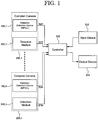
- FIG. 1 shows the arrangement of a radiation image forming apparatus according to this embodiment.
- the radiation image forming apparatus includes a plurality of Compton cameras 200_1 to 200_n (n is an integer), a controller 310, an input device 312, and an output device 314.
- the controller 310 reconstructs a three-dimensional image by computation based on detection signals (S11, ..., S1 n and S21, ..., S2n, where n is an integer (the same applies hereinafter)) output from the Compton cameras 200_1 to 200_n and specifies the position of a specimen (radiation source).
- the operator can instruct the controller 310 by using the input device 312.
- the three-dimensional image reconstructed by the controller 310 is presented to the operator via the output device 314.
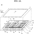
- FIG 2A shows the schematic arrangement of a detection element 113 of a radiation detection device 100.
- the radiation detection device 100 includes the detection element 113 having a pixel electrode portion 101 and connecting terminal portions 109 (109a and 109b) and a drift electrode 110.
- the detection element 113 and the drift electrode 110 are provided in a chamber 111.
- the detection element 113 is an element including the pixel electrode portion 101 and the connecting terminal portions 109 (109a and 109b).
- the pixel electrode portion 101 of the radiation detection device 100 includes an insulating member 102, cathode electrodes 104, anode electrodes 106, anode electrode patterns 108, and a substrate 130.
- the plurality of cathode electrodes 104 are arranged on the first surface of the insulating member 102.
- the cathode electrodes 104 have a plurality of opening portions 105.
- the cathode electrode 104 is formed into a strip shape and hence is also called a cathode strip electrode.
- the anode electrode 106 is placed in a through hole provided in the insulating member 102 from the second surface on the opposite side to the first surface of the insulating member 102.
- the tip ends of the anode electrodes 106 are exposed in the plurality of opening portions 105 in the cathode electrode 104.
- each anode electrode 106 has a shape with its tip end being exposed in a corresponding one of the opening portions 105.
- each anode electrode 106 may be shaped such that its tip end is not exposed in a corresponding one of the opening portions 105 (including an anode electrode shaped such that its tip end is almost flush with the upper surface of the insulating member 102 (the upper surface of the through hole) or its tip end is located inside the through hole of the insulating member 102).
- the plurality of anode electrodes 106 placed in the plurality of opening portions 105 of one cathode electrode 104 are respectively connected to the plurality of anode electrode patterns 108.
- the anode electrode pattern 108 extends to the connecting terminal portion 109a.
- the direction in which the cathode electrode 104 extends is almost vertical to the direction in which the anode electrode pattern 108 extends.
- This embodiment has exemplified the mode in which the anode electrodes 106 and the anode electrode patterns 108 are separately provided and are electrically connected to each other. However, this is not exhaustive, and the anode electrodes 106 and the anode electrode patterns 108 to which the respective anode electrodes 106 are connected may be integrally formed.
- Each anode electrode pattern 108 is formed into a strip shape and hence is also called an anode strip pattern.
- the connecting terminal portion 109a includes a via hole 126 connected to the anode electrode pattern 108 and a metal layer 120.
- the metal layer 120 is connected to the via hole 126.
- Figure 2A shows a case in which the anode electrode patterns 108 and the via holes 126 are separately formed, this is not exhaustive, and the anode electrode patterns 108 and the via holes 126 may be formed from the same metal material.
- the wiring terminal portion 109b includes an electrode 104a which is an extended portion of the cathode electrode 104.
- the radiation detection device 100 has the anode electrodes 106 arranged in a matrix pattern on the pixel electrode portion 101. That is, the radiation detection device 100 has a plurality of "pixels" arranged, each including the anode electrode 106 and a portion of the cathode electrode 104. In this arrangement, a voltage is applied between each cathode electrode 104 and the corresponding anode electrode 106 to form an electric field.
- the drift electrode 110 is placed to face the pixel electrode portion 101.
- the cathode electrodes 104 of the pixel electrode portion 101 are grounded, and a voltage is applied between the drift electrode 110 and each cathode electrode 104 to from an electric field.
- the chamber 111 encloses the pixel electrode portion 101, the connecting terminal portions 109, and the drift electrode 110.
- a gas mixture of a rare gas such as argon or xenon and a molecular gas such as ethane or methane is introduced into the chamber 111.
- FIG 2B shows the schematic arrangement of a detection module 202.
- a Compton camera 200 according to this embodiment includes the radiation detection device 100 using MPGC and the detection module 202.
- the detection module 202 also includes a photomultiplier tube that converts emitted light when a scattered y ray enters the detection module into an electrical signal.
- the detection module 202 is installed so as to surround the radiation detection device 100 from five directions. Referring to Figure 2B , the detection module has five portions 202a to 202e. Note, however, it is not essential that the detection module 202 is installed to surround the radiation detection device 100 from five directions.
- the chamber 111 is attached to the radiation detection device 100.
- a gas mixture of a rare gas such as argon or xenon and an alkane gas (a chain saturate hydrocarbon represented by the general formula C n H 2n+2 ) at room temperature such as ethane or methane or a gas having a quenching effect (quenching gas) including carbon dioxide is introduced into the chamber 111.
- a gas or gases to be mixed with a rare gas may include either or both of a gas such as ethane or methane and a gas having a quenching effect including carbon dioxide.
- the pixel electrode portion 101 on which a plurality of pixels is two-dimensionally laid out is provided on the bottom surface of the chamber 111.
- the drift electrode 110 is provided on the upper surface of the chamber 111.
- Drift cages 112 are provided on side surfaces of the chamber 111. The drift cages 112 are provided to homogenize the electric field distribution between the drift electrode 110 and the pixel electrode portion 101.
- the gas in the chamber 111 which has collided with the incident ⁇ ray emits a recoil electron e - (charged particle) from the position denoted by reference symbol "A" in a predetermined direction.
- An electron cloud is then generated along the track of the recoil electron.
- the electrons constituting the electron cloud are attracted to the pixel electrode portion 101 due to an electric field between the drift electrode 110 and the pixel electrode portion 101.
- An electron that has been attracted collides with the gas to ionize the gas. Ionized electrons proliferate in an avalanche-like manner and are detected by the pixel electrode portion 101.
- the electrical signal obtained in this manner corresponds to the detection signal S1n shown in Figure 1 , and information representing the incident position and time of a scattered y ray is provided to the controller 310.
- the detection signal S2n is a signal that makes it possible to specify the position of a pixel that has detected the electron and the time when the pixel has detected the electron.
- the time between the instant when a scattered ⁇ ray enters the detection module 202 and the instant when an electron is detected by the pixel electrode portion 101 makes it possible to calculate the distance from the pixel electrode portion 101 to the position at which an electron cloud is generated (the position in the z direction).
- the controller 310 is triggered by the activation of the detection signal S1n (the incidence of a scattered y ray on the scintillator) to chronologically analyze the detection signal S2n and calculate the track of a recoil electron by using the position of a pixel that has detected an electron and the time when the pixel has detected the electron (to be sometimes referred to as a detection time hereinafter).
- the detection time (to be sometimes referred to as a drift time hereinafter) corresponds to the time from the instant when the controller 310 is triggered to the instant when an electron is detected by the pixel electrode portion 101. Calculating also an angle ⁇ shown in Figure 2C can specify the direction in which the incident ⁇ ray has entered.
- the pixel electrode portion 101 includes the insulating member 102, the cathode electrodes 104, the anode electrodes 106, and the anode electrode patterns 108.
- the plurality of cathode electrodes 104 extend in the y direction on the upper surface of the insulating member 102.
- the cathode electrode 104 is provided with the plurality of opening portions 105.
- the upper surface of the insulating member 102 is exposed in the opening portions 105.
- the anode electrodes 106 extend from the reverse surface of the insulating member 102 and penetrate through the insulating member 102 in the z direction. The tip ends of the anode electrodes 106 are exposed in the plurality of opening portions 105.
- the plurality of anode electrodes 106 arrayed in the y direction are respectively connected to the different anode electrode patterns 108.
- the plurality of anode electrode patterns 108 extend in the x direction on the reverse surface of the insulating member 102.
- the y direction in which the cathode electrodes 104 extend is almost perpendicular to the x direction in which the anode electrode patterns 108 extend.
- This embodiment has exemplified the mode in which the anode electrodes 106 and the anode electrode patterns 108 are separately provided and are electrically connected to each other. However, this is not exhaustive, and the anode electrodes 106 and the anode electrode patterns 108 may be integrally formed.
- a voltage is applied between the cathode electrode 104 and the anode electrode 106 to form an electric field.
- the anode electrode 106 captures an electron attracted to the pixel electrode portion 101 due to this electric field. This pixel then detects the electron.
- the drift electrode 110 has an xy plane is separated from the xy plane forming the pixel electrode portion 101 by a predetermined distance in the z direction. A voltage is applied between the drift electrode 110 and the cathode electrode 104 and the anode electrode 106 to form an electric field.
- the radiation detection device 100 has the above arrangement, in which the anode electrodes 106 are arranged in a matrix pattern in the pixel electrode portion 101.
- the anode electrode 106 exposed on the upper surface of the insulating member 102 forms one pixel.
- Chronologically analyzing changes in the voltages of electrical signals appearing in the plurality of cathode electrodes 104 and the plurality of anode electrode patterns 108 can specify the positions of pixels that have detected electrons and the detection times of the electrons, thus obtaining electron detection results at the respective pixels. As has been described above, this makes it possible to calculate the track of a recoil electron.
- a plurality of radiation detection devices 100 according to the first embodiment are laid out annularly.
- a specimen (radiation source) as a measurement target is placed in the area surrounded by the radiation detection devices 100.
- the specimen (radiation source) radially emits ⁇ rays, and hence annularly arranging the plurality of radiation detection devices 100 makes it possible to detect more ⁇ rays. This increases the detection frequency of ⁇ rays. Accordingly, when such devices are applied to medical purposes, it is possible to complete imaging in a time shorter than the body motion cycle of the patient as the specimen. In this case, it is possible to greatly reduce position measurement errors with respect to the specimen (radiation source), which are caused by the body motion of the patient.
- a detection module 202 may be allocated to each radiation detection device 100, or one detection module 202 may be allocated to two or more radiation detection devices 100.
- the detection module 202 is preferably provided to surround the radiation detection device 100 from five directions like the structure shown in Figure 2B . This makes the detection module 202 placed between the adjacent radiation detection devices 100 serve as a radiation shielding member, and hence the scattered y rays detected by the detection module 202 can be properly associated with the recoil electrons detected by the radiation detection device 100.
- a radiation shielding member is preferably placed between the adjacent radiation detection devices 100.
- lead may be selected as a material for a radiation shielding member.
- Discrete chambers 111 are preferably used for the radiation detection devices 100 adjacent to each other in the circumferential direction. This is because using a large-scale chamber continuous in the circumferential direction will make it difficult to manufacture the insulating member 102 and will increase the wiring lengths of cathode electrodes 104 and anode electrode patterns 108 to result in an increase in resistance value.
- Using these radiation detection devices 100 and performing arithmetic processing based on detection signals can reconstruct a three-dimensional image and specify the position of the source of radiation that is emitted from a specimen.
- a plurality of radiation detection devices 100 according to the second embodiment are laid out in a double-layer annular pattern. That is, a plurality of radiation detection devices 100a constitute a first detection unit surrounding a specimen (radiation source), and a plurality of other radiation detection devices 100b constitute a second detection unit surrounding the outer circumference of the first detection unit.
- This arrangement makes y rays transmitted through the first detection unit enter the second detection unit, resulting in an increase in the detection frequency of y rays.
- Figure 6 shows the arrangements of the first radiation detection device 100a and the second radiation detection device 100b that are doubly stacked.
- Figure 6 shows a mode in which the second radiation detection device 100b is placed outside the first radiation detection device 100a (on the back side of a pixel electrode portion 101).
- the first radiation detection device 100a and the second radiation detection device 100b each include the pixel electrode portion 101, a drift electrode 110 facing the pixel electrode portion, and a drift cage 112 placed to sandwich the space between the pixel electrode portion and the drift electrode.
- the detection modules 202 may not be interposed between the first and second detection units.
- the two radiation detection devices can be formed by using a command chamber. That is, as shown in Figure 7 , a pixel electrode portion 101 is placed at a predetermined position in the z direction in a chamber 111. The two spaces partitioned by the pixel electrode portion 101 are used as the radiation detection devices 100.
- Figure 7 shows a mode in which a drift electrode 110 is placed to face the pixel electrode on one surface side on which the pixel electrode portion 101 is placed, and a drift cage 112 is placed to sandwich the space between the drift electrode 110 and the pixel electrode, with a similar arrangement being formed on the other surface side on which the pixel electrode portion 101 is placed (for example, the side where detection modules 202 are arranged).
- two detection units each having the pixel electrode portion 101 on one surface, may be stacked on each other so as to arrange the pixel electrode portions 101 on the obverse and reverse surfaces or a detection unit having the pixel electrode portions 101 on the two surfaces may be used.
- Figure 7 shows an example using the detection unit provided with the pixel electrode portions 101 on the two surfaces.
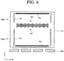
- the insulating member 102 may be provided at an intermediate position in the z direction of the chamber 111, the insulating member 102 may be placed while being offset toward the specimen (radiation source), as shown in Figure 8 . This allocates a wider space in the chamber 111 to second radiation detection devices 100b constituting a second detection unit. Because the dose of y rays decreases with a distance from a specimen (radiation source), allocating a wider space in the chamber 111 to the remoter second detection unit makes it possible to ensure sufficient detection sensitivity.
- a first pixel electrode portion 101a is provided on a first surface 103a of the insulating member 102
- a second pixel electrode portion 101b is provided on a second surface 103b of the insulating member 102.
- the first surface is the upper surface facing the specimen (radiation source) side
- the second surface is the lower surface located on the opposite side to the first surface 103a.
- an anode electrode pattern 108a included in the first pixel electrode portion 101a is provided separately from an anode electrode pattern 108b included in the second pixel electrode portion 101b.
- the plane position of an anode electrode 106 provided on the first surface 103a coincides with the plane position of an anode electrode 106 provided on the second surface 103b.
- an electrode pattern on a first pixel electrode portion 101a differs from an electrode pattern on a second pixel electrode portion 101b. More specifically, the diameter of an anode electrode 106 on the second pixel electrode portion 101b is larger than that of an anode electrode 106 on the first pixel electrode portion 101a. In addition, the opening diameter of an opening portion 105 in the second pixel electrode portion 101b is smaller than that of an opening portion 105 in the first pixel electrode portion 101a.
- This also makes it possible to evaluate a change in detection characteristic due to a difference in electrode pattern.
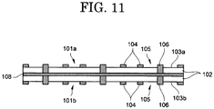
- an insulating member 102 having pixel electrode portions 101 formed on the two surfaces As an insulating member 102 having pixel electrode portions 101 formed on the two surfaces, the structure shown in Figure 9 can be adopted.
- an anode electrode pattern 108 is shared between a first pixel electrode portion 101a and a second pixel electrode portion 101b.
- Other points are the same as those of the structure shown in Figure 9 . Accordingly, the plane position of an anode electrode 106 provided on a first surface 103a coincides with the plane position of an anode electrode 106 provided on a second surface 103b.
- This arrangement omits an insulating member between an anode electrode pattern 108a and an anode electrode pattern 108b like that shown in Figures 9 and 10 , thereby reducing the overall thickness of the insulating member 102.
- this can greatly reduce the number of signal wirings. This makes it possible to reduce the size of the circuit of a signal processing system, thus achieving reductions in size and weight.
- signals from the obverse and reverse surfaces can be separated from each other by using signals obtained from cathode electrodes 104.
- drift electrodes 110a to 110c are arranged at two end positions and an intermediate position in the chamber 111 in the z direction.
- an insulating member 102a is placed between the drift electrode 110a and the drift electrode 110c
- an insulating member 102b is placed between the drift electrode 110b and the drift electrode 110c. That is, the drift electrode 110c is shared between the two radiation detection devices 100b and 100c.
- the insulating members 102a and 102b each have the structure shown in Figure 11 .
- This arrangement is configured to partition the space of the chamber 111 into four spaces, and hence the partitioned spaces can be handled as the four radiation detection devices 100a to 100d. Accordingly, when a plurality of sets of such radiation detection devices 100a to 100d, each as a unit, are annularly arranged, a specimen (radiation source) can be surrounded by four-layer radiation detection devices. This can further increase the detection frequency.
- Arranging a plurality of single-layer detection units, each shown in Figure 4 , in the axis direction can form a tubular arrangement having single-layer detection units continuing coaxially, as shown in Figure 13 .
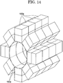
- arranging a plurality of double-layer detection units, each shown in Figure 5 , in the axial direction can form a tubular arrangement having double-layer detection units continuing coaxially, as shown in Figure 14 .
- This can further increase the detection frequency.
- This arrangement allows a wider range of a specimen to be set as a detection target.
- a specimen radiation source
- This arrangement can further increase the detection accuracy.
Landscapes
- Physics & Mathematics (AREA)
- Health & Medical Sciences (AREA)
- Life Sciences & Earth Sciences (AREA)
- General Physics & Mathematics (AREA)
- High Energy & Nuclear Physics (AREA)
- Molecular Biology (AREA)
- Spectroscopy & Molecular Physics (AREA)
- Measurement Of Radiation (AREA)
Abstract
Description
- The present invention relates to a radiation image forming apparatus.
- A radiation detection device (micro pixel gas chamber (MPGC)) using gas amplification by pixel-type electrodes has been studied. A radiation detection device using MPGC is combined with a detection module to form a Compton camera. The Compton camera is featured to implement imaging of a detection region which conventional detectors have not been able to satisfactorily implement.
- Refer to
PTLs 1 and 2 for information about the structure of a radiation detection device using MPGC. -
- PTL 1: Japanese Patent Application Laid-Open No.
2012-255698 - PTL 2: Japanese Patent Application Laid-Open No.
2012-154725 - A Compton camera uses Compton scattering occurring in a gas. However, the probability of Compton scattering in a gas is low. For this reason, a conventional Compton camera using gas amplification exhibits a low detection frequency of y rays, and hence suffers a low detection speed, resulting in taking much time to obtain a sufficient detection signal.
- It is therefore an object of the present invention to provide a radiation image forming apparatus with an increased detection frequency of y rays.
- According to an embodiment of the present invention, there is provided a radiation image forming apparatus including a detection unit including a Compton camera including a radiation detection device that includes a plurality of pixels, each configured to detect an electron generated by the track of a recoil electron generated by Compton scattering, and is configured to output a detection signal configured to specify the position of a pixel that has detected the electron and a time when the pixel has detected the electron, and a detection module configured to detect the incident position of scattered y rays generated by the Compton scattering. The detection unit has a plurality of the Compton cameras arranged annularly to surround a region in which a specimen is placed.
- There is provided a radiation image forming apparatus including a first detection unit and a second detection unit each including a Compton camera including a radiation detection device that includes a plurality of pixels, each configured to detect an electron generated by the track of a recoil electron generated by Compton scattering, and is configured to output a detection signal configured to specify the position of a pixel that has detected the electron and a time when the pixel has detected the electron, and a detection module configured to detect the incident position of scattered y rays generated by the Compton scattering. The first detection unit has a plurality of the Compton cameras arranged annularly to surround a specimen. The second detection unit has a plurality of the Compton cameras arranged annularly to surround the first detection unit.
- A plurality of the detection units may be arranged along an axial direction so as to coaxially surround the specimen.
- A plurality of the first detection units and a plurality of the second detection units may be arranged along an axial direction to coaxially surround the specimen.
- The radiation detection device may include a chamber into which a gas is introduced and an insulating member provided in the chamber, a first radiation detection device included in the first detection unit and a second radiation detection device included in the second detection unit may share the chamber and the insulating member, and a first pixel electrode portion configurating the first radiation detection device may be provided on a first surface of the insulating member, and a second pixel electrode portion configurating the second radiation detection device may be provided on a second surface located on an opposite side to the first surface of the insulating member.
- An electrode pattern of the first pixel electrode portion may differ from an electrode pattern of the second pixel electrode portion.
- The first pixel electrode portion and the second pixel electrode portion each may include a plurality of anode electrodes, and anode electrodes, of the plurality of anode electrodes respectively included in the first pixel electrode portion and the second pixel electrode portion, whose plane positions overlap each other are short-circuited.
- The radiation detection device may include a first radiation detection device included in the first detection unit and a second radiation detection device included in the second detection unit and overlapping the first radiation detection device when viewed from the specimen, the first radiation detection device and the second radiation detection device may include a common chamber, a first insulating member and a second insulating member provided in the chamber, and a drift electrode placed between the first insulating member and the second insulating member, the first insulating member may be provided with the first pixel electrode portion forming the first radiation detection device, and the second insulating member may be provided with the second pixel electrode portion forming the second radiation detection device.
- According to an embodiment and other embodiments of the present invention, it is possible to provide a radiation image forming apparatus with an increased detection frequency of y rays.
-
-
Figure 1 is a block diagram showing the arrangement of an imaging device; -
Figure 2A is a view showing the schematic arrangement of a detection element of a radiation detection device; -
Figure 2B is a view showing the schematic arrangement of a Compton camera; -
Figure 2C a view for explaining the relationship between an incident y ray, a scattered y ray, and a recoil electron; -
Figure 3 is a view showing the schematic arrangement of a radiation detection device; -
Figure 4 is a layout view of a radiation detection device according to the first embodiment; -
Figure 5 is a layout view of a radiation detection device according to the second embodiment; -
Figure 6 is a schematic sectional view of the radiation detection device; -
Figure 7 is a schematic diagram showing an example in which two radiation detection devices are formed in one chamber according to the third embodiment; -
Figure 8 is a schematic diagram showing another example in which two radiation detection devices are formed in one chamber according to the third embodiment; -
Figure 9 is a schematic diagram for explaining the structure of an insulating member according to the fourth embodiment; -
Figure 10 a schematic diagram for explaining the structure of an insulating member according to the fifth embodiment; -
Figure 11 a schematic diagram for explaining the structure of an insulating member according to the sixth embodiment; -
Figure 12 is a schematic diagram showing an example in which four radiation detection devices are formed in one chamber according to the seventh embodiment; -
Figure 13 is a schematic diagram showing an example in which a plurality of single-layer rings are arranged in the axial direction according to the eighth embodiment; and -
Figure 14 is a schematic diagram showing an example in which a plurality of double-layer rings are arranged in the axial direction according to the eighth embodiment. - A radiation image forming apparatus according to the present invention will be described in detail below with reference to the accompanying drawings. Note that the radiation image forming apparatus according to the present invention is not limited to the following embodiments and can be variously modified and embodied. In the description of the embodiments disclosed in this specification, the same reference numerals denote the same constituent elements. Furthermore, for the sake of descriptive convenience, dimensional ratios in the accompanying drawings are sometimes different from actual ratios, and an illustration of some components is sometimes omitted from the drawings.
-
Figure 1 shows the arrangement of a radiation image forming apparatus according to this embodiment. The radiation image forming apparatus includes a plurality of Compton cameras 200_1 to 200_n (n is an integer), acontroller 310, aninput device 312, and anoutput device 314. - The
controller 310 reconstructs a three-dimensional image by computation based on detection signals (S11, ..., S1 n and S21, ..., S2n, where n is an integer (the same applies hereinafter)) output from the Compton cameras 200_1 to 200_n and specifies the position of a specimen (radiation source). The operator can instruct thecontroller 310 by using theinput device 312. The three-dimensional image reconstructed by thecontroller 310 is presented to the operator via theoutput device 314. -
Figure 2A shows the schematic arrangement of adetection element 113 of aradiation detection device 100. Theradiation detection device 100 includes thedetection element 113 having apixel electrode portion 101 and connecting terminal portions 109 (109a and 109b) and adrift electrode 110. Thedetection element 113 and thedrift electrode 110 are provided in achamber 111. Thedetection element 113 is an element including thepixel electrode portion 101 and the connecting terminal portions 109 (109a and 109b). - The
pixel electrode portion 101 of theradiation detection device 100 includes an insulatingmember 102,cathode electrodes 104,anode electrodes 106,anode electrode patterns 108, and asubstrate 130. The plurality ofcathode electrodes 104 are arranged on the first surface of theinsulating member 102. Thecathode electrodes 104 have a plurality ofopening portions 105. Thecathode electrode 104 is formed into a strip shape and hence is also called a cathode strip electrode. - The
anode electrode 106 is placed in a through hole provided in theinsulating member 102 from the second surface on the opposite side to the first surface of theinsulating member 102. In this embodiment, the tip ends of theanode electrodes 106 are exposed in the plurality of openingportions 105 in thecathode electrode 104. Referring toFigure 2A , eachanode electrode 106 has a shape with its tip end being exposed in a corresponding one of the openingportions 105. However, eachanode electrode 106 may be shaped such that its tip end is not exposed in a corresponding one of the opening portions 105 (including an anode electrode shaped such that its tip end is almost flush with the upper surface of the insulating member 102 (the upper surface of the through hole) or its tip end is located inside the through hole of the insulating member 102). - The plurality of
anode electrodes 106 placed in the plurality of openingportions 105 of onecathode electrode 104 are respectively connected to the plurality ofanode electrode patterns 108. Theanode electrode pattern 108 extends to the connectingterminal portion 109a. The direction in which thecathode electrode 104 extends is almost vertical to the direction in which theanode electrode pattern 108 extends. This embodiment has exemplified the mode in which theanode electrodes 106 and theanode electrode patterns 108 are separately provided and are electrically connected to each other. However, this is not exhaustive, and theanode electrodes 106 and theanode electrode patterns 108 to which therespective anode electrodes 106 are connected may be integrally formed. Eachanode electrode pattern 108 is formed into a strip shape and hence is also called an anode strip pattern. - The connecting
terminal portion 109a includes a viahole 126 connected to theanode electrode pattern 108 and ametal layer 120. Themetal layer 120 is connected to the viahole 126. AlthoughFigure 2A shows a case in which theanode electrode patterns 108 and the via holes 126 are separately formed, this is not exhaustive, and theanode electrode patterns 108 and the via holes 126 may be formed from the same metal material. Thewiring terminal portion 109b includes anelectrode 104a which is an extended portion of thecathode electrode 104. - With the above arrangement, the
radiation detection device 100 has theanode electrodes 106 arranged in a matrix pattern on thepixel electrode portion 101. That is, theradiation detection device 100 has a plurality of "pixels" arranged, each including theanode electrode 106 and a portion of thecathode electrode 104. In this arrangement, a voltage is applied between eachcathode electrode 104 and the correspondinganode electrode 106 to form an electric field. - The
drift electrode 110 is placed to face thepixel electrode portion 101. Thecathode electrodes 104 of thepixel electrode portion 101 are grounded, and a voltage is applied between thedrift electrode 110 and eachcathode electrode 104 to from an electric field. - The
chamber 111 encloses thepixel electrode portion 101, the connecting terminal portions 109, and thedrift electrode 110. A gas mixture of a rare gas such as argon or xenon and a molecular gas such as ethane or methane is introduced into thechamber 111. -
Figure 2B shows the schematic arrangement of adetection module 202. As shown inFigure 2B , aCompton camera 200 according to this embodiment includes theradiation detection device 100 using MPGC and thedetection module 202. In this case, thedetection module 202 also includes a photomultiplier tube that converts emitted light when a scattered y ray enters the detection module into an electrical signal. As shown inFigure 2B , thedetection module 202 is installed so as to surround theradiation detection device 100 from five directions. Referring toFigure 2B , the detection module has five portions 202a to 202e. Note, however, it is not essential that thedetection module 202 is installed to surround theradiation detection device 100 from five directions. - The
chamber 111 is attached to theradiation detection device 100. A gas mixture of a rare gas such as argon or xenon and an alkane gas (a chain saturate hydrocarbon represented by the general formula CnH2n+2) at room temperature such as ethane or methane or a gas having a quenching effect (quenching gas) including carbon dioxide is introduced into thechamber 111. A gas or gases to be mixed with a rare gas may include either or both of a gas such as ethane or methane and a gas having a quenching effect including carbon dioxide. Thepixel electrode portion 101 on which a plurality of pixels is two-dimensionally laid out is provided on the bottom surface of thechamber 111. Thedrift electrode 110 is provided on the upper surface of thechamber 111.Drift cages 112 are provided on side surfaces of thechamber 111. Thedrift cages 112 are provided to homogenize the electric field distribution between thedrift electrode 110 and thepixel electrode portion 101. - The following description concerns the principle of the
Compton camera 200. First of all, when a y ray externally enters theradiation detection device 100, the incident y ray collides with a gas in thechamber 111 and is scattered at a certain probability. Reference symbol "A" inFigure 2B denotes a collision position. The scattered y ray whose propagation direction is changed by the collision is transmitted through theradiation detection device 100 and enters thedetection module 202. When the scattered y ray enters thedetection module 202, light emission occurs. A photomultiplier tube then converts this emitted light into an electrical signal. - On the other hand, the gas in the
chamber 111 which has collided with the incident γ ray emits a recoil electron e- (charged particle) from the position denoted by reference symbol "A" in a predetermined direction. An electron cloud is then generated along the track of the recoil electron. The electrons constituting the electron cloud are attracted to thepixel electrode portion 101 due to an electric field between thedrift electrode 110 and thepixel electrode portion 101. An electron that has been attracted collides with the gas to ionize the gas. Ionized electrons proliferate in an avalanche-like manner and are detected by thepixel electrode portion 101. The electrical signal obtained in this manner corresponds to the detection signal S1n shown inFigure 1 , and information representing the incident position and time of a scattered y ray is provided to thecontroller 310. The detection signal S2n is a signal that makes it possible to specify the position of a pixel that has detected the electron and the time when the pixel has detected the electron. - Note that the time between the instant when a scattered γ ray enters the
detection module 202 and the instant when an electron is detected by thepixel electrode portion 101 makes it possible to calculate the distance from thepixel electrode portion 101 to the position at which an electron cloud is generated (the position in the z direction). - The
controller 310 is triggered by the activation of the detection signal S1n (the incidence of a scattered y ray on the scintillator) to chronologically analyze the detection signal S2n and calculate the track of a recoil electron by using the position of a pixel that has detected an electron and the time when the pixel has detected the electron (to be sometimes referred to as a detection time hereinafter). The detection time (to be sometimes referred to as a drift time hereinafter) corresponds to the time from the instant when thecontroller 310 is triggered to the instant when an electron is detected by thepixel electrode portion 101. Calculating also an angle α shown inFigure 2C can specify the direction in which the incident γ ray has entered. - As shown in
Figure 3 , thepixel electrode portion 101 includes the insulatingmember 102, thecathode electrodes 104, theanode electrodes 106, and theanode electrode patterns 108. - The plurality of
cathode electrodes 104 extend in the y direction on the upper surface of the insulatingmember 102. Thecathode electrode 104 is provided with the plurality of openingportions 105. The upper surface of the insulatingmember 102 is exposed in the openingportions 105. - The
anode electrodes 106 extend from the reverse surface of the insulatingmember 102 and penetrate through the insulatingmember 102 in the z direction. The tip ends of theanode electrodes 106 are exposed in the plurality of openingportions 105. - The plurality of
anode electrodes 106 arrayed in the y direction are respectively connected to the differentanode electrode patterns 108. The plurality ofanode electrode patterns 108 extend in the x direction on the reverse surface of the insulatingmember 102. The y direction in which thecathode electrodes 104 extend is almost perpendicular to the x direction in which theanode electrode patterns 108 extend. This embodiment has exemplified the mode in which theanode electrodes 106 and theanode electrode patterns 108 are separately provided and are electrically connected to each other. However, this is not exhaustive, and theanode electrodes 106 and theanode electrode patterns 108 may be integrally formed. - A voltage is applied between the
cathode electrode 104 and theanode electrode 106 to form an electric field. Theanode electrode 106 captures an electron attracted to thepixel electrode portion 101 due to this electric field. This pixel then detects the electron. - The
drift electrode 110 has an xy plane is separated from the xy plane forming thepixel electrode portion 101 by a predetermined distance in the z direction. A voltage is applied between thedrift electrode 110 and thecathode electrode 104 and theanode electrode 106 to form an electric field. - The
radiation detection device 100 according to this embodiment has the above arrangement, in which theanode electrodes 106 are arranged in a matrix pattern in thepixel electrode portion 101. Theanode electrode 106 exposed on the upper surface of the insulatingmember 102 forms one pixel. Chronologically analyzing changes in the voltages of electrical signals appearing in the plurality ofcathode electrodes 104 and the plurality ofanode electrode patterns 108 can specify the positions of pixels that have detected electrons and the detection times of the electrons, thus obtaining electron detection results at the respective pixels. As has been described above, this makes it possible to calculate the track of a recoil electron. - As shown in
Figure 4 , a plurality ofradiation detection devices 100 according to the first embodiment are laid out annularly. A specimen (radiation source) as a measurement target is placed in the area surrounded by theradiation detection devices 100. - The specimen (radiation source) radially emits γ rays, and hence annularly arranging the plurality of
radiation detection devices 100 makes it possible to detect more γ rays. This increases the detection frequency of γ rays. Accordingly, when such devices are applied to medical purposes, it is possible to complete imaging in a time shorter than the body motion cycle of the patient as the specimen. In this case, it is possible to greatly reduce position measurement errors with respect to the specimen (radiation source), which are caused by the body motion of the patient. - In this case, a
detection module 202 may be allocated to eachradiation detection device 100, or onedetection module 202 may be allocated to two or moreradiation detection devices 100. When thedetection module 202 is allocated to eachradiation detection device 100, thedetection module 202 is preferably provided to surround theradiation detection device 100 from five directions like the structure shown inFigure 2B . This makes thedetection module 202 placed between the adjacentradiation detection devices 100 serve as a radiation shielding member, and hence the scattered y rays detected by thedetection module 202 can be properly associated with the recoil electrons detected by theradiation detection device 100. - It is also possible to place the
detection module 202 on only the bottom surface of theradiation detection device 100 without placing anydetection modules 202 on the side surfaces of theradiation detection device 100. In this case, in order to prevent scattered y rays from entering anotherradiation detection device 100, a radiation shielding member is preferably placed between the adjacentradiation detection devices 100. For example, lead may be selected as a material for a radiation shielding member. -
Discrete chambers 111 are preferably used for theradiation detection devices 100 adjacent to each other in the circumferential direction. This is because using a large-scale chamber continuous in the circumferential direction will make it difficult to manufacture the insulatingmember 102 and will increase the wiring lengths ofcathode electrodes 104 andanode electrode patterns 108 to result in an increase in resistance value. - Using these
radiation detection devices 100 and performing arithmetic processing based on detection signals can reconstruct a three-dimensional image and specify the position of the source of radiation that is emitted from a specimen. - As shown in
Figure 5 , a plurality ofradiation detection devices 100 according to the second embodiment are laid out in a double-layer annular pattern. That is, a plurality ofradiation detection devices 100a constitute a first detection unit surrounding a specimen (radiation source), and a plurality of otherradiation detection devices 100b constitute a second detection unit surrounding the outer circumference of the first detection unit. This arrangement makes y rays transmitted through the first detection unit enter the second detection unit, resulting in an increase in the detection frequency of y rays. -
Figure 6 shows the arrangements of the firstradiation detection device 100a and the secondradiation detection device 100b that are doubly stacked.Figure 6 shows a mode in which the secondradiation detection device 100b is placed outside the firstradiation detection device 100a (on the back side of a pixel electrode portion 101). The firstradiation detection device 100a and the secondradiation detection device 100b each include thepixel electrode portion 101, adrift electrode 110 facing the pixel electrode portion, and adrift cage 112 placed to sandwich the space between the pixel electrode portion and the drift electrode. As shown inFigure 5 , when a plurality of radiation detection devices is stacked on each other, becausedetection modules 202 are radiation shielding members, thedetection modules 202 may not be interposed between the first and second detection units. For example, as shown inFigure 6 , it is possible to use an arrangement in which thedetection modules 202 arranged on the bottom surface side of each secondradiation detection device 100b constituting the second detection unit, and nodetection modules 202 are arranged around each firstradiation detection device 100a constituting the first detection unit. - There is conceivable a method of increasing the detection frequency of y rays by increasing the height of a
chamber 111 in the z direction instead of stacking the tworadiation detection devices 100. However, increasing the height of thechamber 111 in the z direction will prolong the time taken for electrons constituting an electron cloud to reach thepixel electrode portion 101. This increases the probability that another Compton scattering will occur during this time. Such multiple scattering and a plurality of occurrences of scattering make it difficult to perform data analysis. This also poses the problem that the sampling rate increases, or discharge is caused by ion feedback. In contrast to this, this embodiment uses the tworadiation detection devices 100 in a stacked state, and hence can increase the detection frequency of y rays while preventing the occurrence of multiple scattering. - As in the second embodiment described above, when two
radiation detection devices 100 are stacked on each other, the two radiation detection devices can be formed by using a command chamber. That is, as shown inFigure 7 , apixel electrode portion 101 is placed at a predetermined position in the z direction in achamber 111. The two spaces partitioned by thepixel electrode portion 101 are used as theradiation detection devices 100.Figure 7 shows a mode in which adrift electrode 110 is placed to face the pixel electrode on one surface side on which thepixel electrode portion 101 is placed, and adrift cage 112 is placed to sandwich the space between thedrift electrode 110 and the pixel electrode, with a similar arrangement being formed on the other surface side on which thepixel electrode portion 101 is placed (for example, the side wheredetection modules 202 are arranged). - In this case, two detection units, each having the
pixel electrode portion 101 on one surface, may be stacked on each other so as to arrange thepixel electrode portions 101 on the obverse and reverse surfaces or a detection unit having thepixel electrode portions 101 on the two surfaces may be used.Figure 7 shows an example using the detection unit provided with thepixel electrode portions 101 on the two surfaces. According to this embodiment, because the tworadiation detection devices 100 are formed by using onechamber 111, the device arrangement can be simplified. This also contributes to a reduction in cost. In addition, there is no need to perform mechanical positioning with respect to the two upper and lowerradiation detection devices 100, and hence more accurate imaging can be implemented. - Although the insulating
member 102 may be provided at an intermediate position in the z direction of thechamber 111, the insulatingmember 102 may be placed while being offset toward the specimen (radiation source), as shown inFigure 8 . This allocates a wider space in thechamber 111 to secondradiation detection devices 100b constituting a second detection unit. Because the dose of y rays decreases with a distance from a specimen (radiation source), allocating a wider space in thechamber 111 to the remoter second detection unit makes it possible to ensure sufficient detection sensitivity. - As an insulating
member 102 provided withpixel electrode portions 101 on the two surfaces, the structure shown inFigure 9 can be adopted. As shown inFigure 9 , a firstpixel electrode portion 101a is provided on afirst surface 103a of the insulatingmember 102, and a secondpixel electrode portion 101b is provided on asecond surface 103b of the insulatingmember 102. In this case, the first surface is the upper surface facing the specimen (radiation source) side, and the second surface is the lower surface located on the opposite side to thefirst surface 103a. - In this embodiment, an
anode electrode pattern 108a included in the firstpixel electrode portion 101a is provided separately from ananode electrode pattern 108b included in the secondpixel electrode portion 101b. This makes it possible to individually set anode-cathode voltages at the firstpixel electrode portion 101a and the secondpixel electrode portion 101b. This makes it possible to individually adjust, for example, the sensitivity of firstradiation detection devices 100a constituting a first detection unit and the sensitivity of secondradiation detection devices 100b constituting a second detection unit. This further makes it possible to evaluate a change in detection characteristic due to a difference in anode-cathode voltage. - In this embodiment, the plane position of an
anode electrode 106 provided on thefirst surface 103a coincides with the plane position of ananode electrode 106 provided on thesecond surface 103b. - As an insulating
member 102 provided withpixel electrode portions 101 on the two surfaces, the structure shown inFigure 10 can be adopted. In this embodiment, as shown inFigure 10 , an electrode pattern on a firstpixel electrode portion 101a differs from an electrode pattern on a secondpixel electrode portion 101b. More specifically, the diameter of ananode electrode 106 on the secondpixel electrode portion 101b is larger than that of ananode electrode 106 on the firstpixel electrode portion 101a. In addition, the opening diameter of anopening portion 105 in the secondpixel electrode portion 101b is smaller than that of anopening portion 105 in the firstpixel electrode portion 101a. - This can increase the strength of an electric field formed between the anode and the cathode on the second
pixel electrode portion 101b relative to the strength of an electric field formed between the anode and the cathode on the firstpixel electrode portion 101a, thereby implementing imaging with different sensing characteristics. This also makes it possible to evaluate a change in detection characteristic due to a difference in electrode pattern. Furthermore, it is possible to optimize the firstpixel electrode portion 101a and the secondpixel electrode portion 101b with respect to difference radiation sources. - As an insulating
member 102 havingpixel electrode portions 101 formed on the two surfaces, the structure shown inFigure 9 can be adopted. In this embodiment, as shown inFigure 11 , ananode electrode pattern 108 is shared between a firstpixel electrode portion 101a and a secondpixel electrode portion 101b. Other points are the same as those of the structure shown inFigure 9 . Accordingly, the plane position of ananode electrode 106 provided on afirst surface 103a coincides with the plane position of ananode electrode 106 provided on asecond surface 103b. - This arrangement omits an insulating member between an
anode electrode pattern 108a and ananode electrode pattern 108b like that shown inFigures 9 and10 , thereby reducing the overall thickness of the insulatingmember 102. In addition, this can greatly reduce the number of signal wirings. This makes it possible to reduce the size of the circuit of a signal processing system, thus achieving reductions in size and weight. In this embodiment, signals from the obverse and reverse surfaces can be separated from each other by using signals obtained fromcathode electrodes 104. Furthermore, according to this embodiment, it is possible to form a through hole through which theanode electrode 106 extends by drilling the insulatingmember 102. - As shown in
Figure 12 , fourradiation detection devices 100a to 100d are provided in onechamber 111 according to the seventh embodiment. More specifically,drift electrodes 110a to 110c are arranged at two end positions and an intermediate position in thechamber 111 in the z direction. In addition, an insulatingmember 102a is placed between thedrift electrode 110a and thedrift electrode 110c, and an insulatingmember 102b is placed between thedrift electrode 110b and thedrift electrode 110c. That is, thedrift electrode 110c is shared between the tworadiation detection devices members Figure 11 . - This arrangement is configured to partition the space of the
chamber 111 into four spaces, and hence the partitioned spaces can be handled as the fourradiation detection devices 100a to 100d. Accordingly, when a plurality of sets of suchradiation detection devices 100a to 100d, each as a unit, are annularly arranged, a specimen (radiation source) can be surrounded by four-layer radiation detection devices. This can further increase the detection frequency. - Arranging a plurality of single-layer detection units, each shown in
Figure 4 , in the axis direction can form a tubular arrangement having single-layer detection units continuing coaxially, as shown inFigure 13 . In addition, arranging a plurality of double-layer detection units, each shown inFigure 5 , in the axial direction can form a tubular arrangement having double-layer detection units continuing coaxially, as shown inFigure 14 . This can further increase the detection frequency. This arrangement allows a wider range of a specimen to be set as a detection target. Although not shown, a specimen (radiation source) may be spherically surrounded by a plurality ofradiation detection devices 100. This arrangement can further increase the detection accuracy. -
- 100, 100a - 100d...radiation detection device; 101, 101a, 101b...pixel electrode portion; 102, 102a, 102b...insulating member; 103a...first surface; 103b...second surface; 104...cathode electrode; 105...opening portion; 106...anode electrode; 108, 108a, 108b...anode electrode pattern; 110, 110a - 110c...drift electrode; 111...chamber; 112...drift cage; 113...detection element; 200...Compton camera; 202 (102a - 202e)...detection module; 310...controller; 312...input device; 314...output device
Claims (8)
- A radiation image forming apparatus, comprising:a detection unit including a Compton camera including a radiation detection device that includes a plurality of pixels, each configured to detect an electron generated by a track of a recoil electron generated by Compton scattering, and is configured to output a detection signal configured to specify a position of a pixel that has detected the electron and a time when the pixel has detected the electron, and a detection module configured to detect an incident position of scattered γ rays generated by the Compton scattering,the detection unit having a plurality of the Compton cameras arranged annularly to surround a region in which a specimen is placed.
- A radiation image forming apparatus, comprising:a first detection unit and a second detection unit each including a Compton camera including a radiation detection device that includes a plurality of pixels, each configured to detect an electron generated by a track of a recoil electron generated by Compton scattering, and is configured to output a detection signal configured to specify a position of a pixel that has detected the electron and a time when the pixel has detected the electron, and a detection module configured to detect an incident position of scattered y rays generated by the Compton scattering,the first detection unit having a plurality of the Compton cameras arranged annularly to surround a specimen, and the second detection unit having a plurality of the Compton cameras arranged annularly to surround the first detection unit.
- The radiation image forming apparatus according to claim 1,
wherein a plurality of the detection units is arranged along an axial direction to coaxially surround the specimen. - The radiation image forming apparatus according to claim 2,
wherein a plurality of the first detection units and a plurality of the second detection units are arranged along an axial direction to coaxially surround the specimen. - The radiation image forming apparatus according to claim 2,
wherein the radiation detection device includes a chamber into which a gas is introduced, and an insulating member provided in the chamber,
wherein a first radiation detection device included in the first detection unit and a second radiation detection device included in the second detection unit share the chamber and the insulating member, and
wherein a first pixel electrode portion configurating the first radiation detection device is provided on a first surface of the insulating member, and a second pixel electrode portion configurating the second radiation detection device is provided on a second surface located on an opposite side to the first surface of the insulating member. - The radiation image forming apparatus according to claim 5,
wherein an electrode pattern of the first pixel electrode portion differs from an electrode pattern of the second pixel electrode portion. - The radiation image forming apparatus according to claim 5,
wherein the first pixel electrode portion and the second pixel electrode portion each include a plurality of anode electrodes, and
wherein anode electrodes, of the plurality of anode electrodes respectively included in the first pixel electrode portion and the second pixel electrode portion, whose plane positions overlap each other are short-circuited. - The radiation image forming apparatus according to claim 2,
wherein the radiation detection device includes a first radiation detection device included in the first detection unit and a second radiation detection device included in the second detection unit and overlapping the first radiation detection device when viewed from the specimen,
wherein the first radiation detection device and the second radiation detection device include a common chamber, a first insulating member and a second insulating member provided in the chamber, and a drift electrode placed between the first insulating member and the second insulating member,
wherein the first insulating member is provided with a first pixel electrode portion forming the first radiation detection device, and
wherein the second insulating member is provided with a second pixel electrode portion forming the second radiation detection device.
Applications Claiming Priority (2)
| Application Number | Priority Date | Filing Date | Title |
|---|---|---|---|
| JP2015195142 | 2015-09-30 | ||
| PCT/JP2016/079008 WO2017057674A1 (en) | 2015-09-30 | 2016-09-30 | Radiation image forming device |
Publications (3)
| Publication Number | Publication Date |
|---|---|
| EP3358374A1 true EP3358374A1 (en) | 2018-08-08 |
| EP3358374A4 EP3358374A4 (en) | 2019-06-26 |
| EP3358374B1 EP3358374B1 (en) | 2022-03-30 |
Family
ID=58423910
Family Applications (1)
| Application Number | Title | Priority Date | Filing Date |
|---|---|---|---|
| EP16851843.9A Active EP3358374B1 (en) | 2015-09-30 | 2016-09-30 | Radiation image forming apparatus |
Country Status (4)
| Country | Link |
|---|---|
| US (1) | US10359521B2 (en) |
| EP (1) | EP3358374B1 (en) |
| JP (1) | JP6780649B2 (en) |
| WO (1) | WO2017057674A1 (en) |
Families Citing this family (2)
| Publication number | Priority date | Publication date | Assignee | Title |
|---|---|---|---|---|
| US12048571B2 (en) | 2018-08-07 | 2024-07-30 | Siemens Medical Solutions Usa, Inc. | Near 2Pi Compton camera for medical imaging |
| WO2022071549A1 (en) | 2020-10-01 | 2022-04-07 | 大日本印刷株式会社 | Detection device |
Family Cites Families (13)
| Publication number | Priority date | Publication date | Assignee | Title |
|---|---|---|---|---|
| JPH079460B2 (en) * | 1987-10-12 | 1995-02-01 | 三菱電機株式会社 | Monitor for particle beam measurement |
| JP3535045B2 (en) | 1999-07-01 | 2004-06-07 | 独立行政法人 科学技術振興機構 | Device for determining gamma-ray incident direction from trajectory image of recoil electrons by MSGC |
| US6791090B2 (en) * | 2000-05-17 | 2004-09-14 | Koninklijke Philips Electronics N.V. | Compton deconvolution camera |
| JP3354551B2 (en) | 2000-06-27 | 2002-12-09 | 科学技術振興事業団 | Particle beam image detector using gas amplification with pixel electrodes |
| JP2008232971A (en) * | 2007-03-23 | 2008-10-02 | Hitachi Medical Corp | Nuclear medicine diagnostic device and photon measuring device |
| JP5393102B2 (en) * | 2008-10-22 | 2014-01-22 | 株式会社日立メディコ | Nuclear medicine diagnostic equipment |
| US8084742B1 (en) * | 2010-03-10 | 2011-12-27 | Radiation Monitoring Devices, Inc. | Positron emission tomography with phoswich detector, systems and methods |
| JP5853370B2 (en) | 2011-01-25 | 2016-02-09 | 大日本印刷株式会社 | Radiation detector using gas amplification |
| JP5772258B2 (en) | 2011-06-08 | 2015-09-02 | 大日本印刷株式会社 | Radiation detector using gas amplification, and radiation detection method using gas amplification |
| US8901557B2 (en) * | 2012-06-15 | 2014-12-02 | Semiconductor Energy Laboratory Co., Ltd. | Semiconductor device |
| JP2015148448A (en) * | 2014-02-04 | 2015-08-20 | キヤノン株式会社 | Charged particle detection device, and gamma camera |
| JP2016118426A (en) * | 2014-12-19 | 2016-06-30 | キヤノン株式会社 | Radiation measurement device |
| JP6551003B2 (en) * | 2015-07-24 | 2019-07-31 | 三菱重工業株式会社 | Radiation measurement apparatus and radiation measurement method |
-
2016
- 2016-09-30 JP JP2017543614A patent/JP6780649B2/en active Active
- 2016-09-30 WO PCT/JP2016/079008 patent/WO2017057674A1/en not_active Ceased
- 2016-09-30 EP EP16851843.9A patent/EP3358374B1/en active Active
-
2018
- 2018-03-26 US US15/935,097 patent/US10359521B2/en active Active
Also Published As
| Publication number | Publication date |
|---|---|
| WO2017057674A1 (en) | 2017-04-06 |
| JP6780649B2 (en) | 2020-11-04 |
| EP3358374A4 (en) | 2019-06-26 |
| JPWO2017057674A1 (en) | 2018-07-19 |
| EP3358374B1 (en) | 2022-03-30 |
| US10359521B2 (en) | 2019-07-23 |
| US20180239036A1 (en) | 2018-08-23 |
Similar Documents
| Publication | Publication Date | Title |
|---|---|---|
| JP3863872B2 (en) | Positron emission tomography system | |
| CN105990089B (en) | A kind of measurement apparatus for space ion and neutral atom | |
| Patra et al. | Measurement of basic characteristics and gain uniformity of a triple GEM detector | |
| EP1640712B1 (en) | Time-resolved measurement device and position-sensitive electron multiplier tube | |
| Stelzer et al. | The new small wheel upgrade project of the ATLAS experiment | |
| US10359521B2 (en) | Radiation image forming apparatus | |
| EP2496966B1 (en) | Charge read-out structure for a photon/particle detector | |
| CN117074804B (en) | An integrated detection device for space charged particles and neutral particles | |
| WO2016140371A1 (en) | Radiation detection method and compton camera | |
| CN114551210B (en) | Photodetector array anodes and multi-anode photomultiplier tubes | |
| EP3677931B1 (en) | Positron tomography device using micropattern detector | |
| KR101825558B1 (en) | Dual energy x-ray detection device, and x-ray imaging system using of multiple gem detector | |
| JP6665470B2 (en) | Radiation detection device and controller | |
| Mei et al. | Topmetal CMOS direct charge sensing plane for neutrinoless double-beta decay search in high-pressure gaseous TPC | |
| JP5136736B2 (en) | Radiation image detection module and radiation image detection apparatus | |
| Caruggi et al. | Development of a data analysis software for the XR-GEM installed at HVPTF and preliminary results | |
| Caruggi et al. | Analysis of micro‐discharges fine dynamics via x‐ray detection on the high voltage Padova test facility experiment | |
| JP2016118426A (en) | Radiation measurement device | |
| Friedman et al. | Large-area plasma-panel radiation detectors for nuclear medicine imaging to homeland security and the super large hadron collider | |
| Beal et al. | Gas-Based Detectors | |
| A Filho et al. | A TDC-based system for X-ray imaging detectors | |
| JP2019184259A (en) | Microstrip gas detector, scintillation camera device, and tomographic apparatus | |
| Simone | Development and characterization of the Fast Timing Micro-pattern gaseous detector | |
| Wang et al. | The beam-particle monitor for CEE experiment | |
| Biebel et al. | Calibration of large area Micromegas detectors using cosmic rays |
Legal Events
| Date | Code | Title | Description |
|---|---|---|---|
| STAA | Information on the status of an ep patent application or granted ep patent |
Free format text: STATUS: THE INTERNATIONAL PUBLICATION HAS BEEN MADE |
|
| PUAI | Public reference made under article 153(3) epc to a published international application that has entered the european phase |
Free format text: ORIGINAL CODE: 0009012 |
|
| STAA | Information on the status of an ep patent application or granted ep patent |
Free format text: STATUS: REQUEST FOR EXAMINATION WAS MADE |
|
| 17P | Request for examination filed |
Effective date: 20180419 |
|
| AK | Designated contracting states |
Kind code of ref document: A1 Designated state(s): AL AT BE BG CH CY CZ DE DK EE ES FI FR GB GR HR HU IE IS IT LI LT LU LV MC MK MT NL NO PL PT RO RS SE SI SK SM TR |
|
| AX | Request for extension of the european patent |
Extension state: BA ME |
|
| DAV | Request for validation of the european patent (deleted) | ||
| DAX | Request for extension of the european patent (deleted) | ||
| A4 | Supplementary search report drawn up and despatched |
Effective date: 20190523 |
|
| RIC1 | Information provided on ipc code assigned before grant |
Ipc: H01J 47/06 20060101ALI20190517BHEP Ipc: G01T 1/18 20060101AFI20190517BHEP Ipc: G01T 1/20 20060101ALI20190517BHEP Ipc: G01T 1/29 20060101ALI20190517BHEP |
|
| STAA | Information on the status of an ep patent application or granted ep patent |
Free format text: STATUS: EXAMINATION IS IN PROGRESS |
|
| 17Q | First examination report despatched |
Effective date: 20200602 |
|
| GRAP | Despatch of communication of intention to grant a patent |
Free format text: ORIGINAL CODE: EPIDOSNIGR1 |
|
| STAA | Information on the status of an ep patent application or granted ep patent |
Free format text: STATUS: GRANT OF PATENT IS INTENDED |
|
| INTG | Intention to grant announced |
Effective date: 20210618 |
|
| RIN1 | Information on inventor provided before grant (corrected) |
Inventor name: OTA, KOHEI Inventor name: OHNO, MOTONORI |
|
| GRAJ | Information related to disapproval of communication of intention to grant by the applicant or resumption of examination proceedings by the epo deleted |
Free format text: ORIGINAL CODE: EPIDOSDIGR1 |
|
| STAA | Information on the status of an ep patent application or granted ep patent |
Free format text: STATUS: EXAMINATION IS IN PROGRESS |
|
| GRAP | Despatch of communication of intention to grant a patent |
Free format text: ORIGINAL CODE: EPIDOSNIGR1 |
|
| STAA | Information on the status of an ep patent application or granted ep patent |
Free format text: STATUS: GRANT OF PATENT IS INTENDED |
|
| GRAJ | Information related to disapproval of communication of intention to grant by the applicant or resumption of examination proceedings by the epo deleted |
Free format text: ORIGINAL CODE: EPIDOSDIGR1 |
|
| GRAP | Despatch of communication of intention to grant a patent |
Free format text: ORIGINAL CODE: EPIDOSNIGR1 |
|
| INTC | Intention to grant announced (deleted) | ||
| INTG | Intention to grant announced |
Effective date: 20211012 |
|
| INTG | Intention to grant announced |
Effective date: 20211028 |
|
| GRAS | Grant fee paid |
Free format text: ORIGINAL CODE: EPIDOSNIGR3 |
|
| GRAA | (expected) grant |
Free format text: ORIGINAL CODE: 0009210 |
|
| STAA | Information on the status of an ep patent application or granted ep patent |
Free format text: STATUS: THE PATENT HAS BEEN GRANTED |
|
| AK | Designated contracting states |
Kind code of ref document: B1 Designated state(s): AL AT BE BG CH CY CZ DE DK EE ES FI FR GB GR HR HU IE IS IT LI LT LU LV MC MK MT NL NO PL PT RO RS SE SI SK SM TR |
|
| REG | Reference to a national code |
Ref country code: GB Ref legal event code: FG4D |
|
| REG | Reference to a national code |
Ref country code: CH Ref legal event code: EP |
|
| REG | Reference to a national code |
Ref country code: DE Ref legal event code: R096 Ref document number: 602016070596 Country of ref document: DE |
|
| REG | Reference to a national code |
Ref country code: AT Ref legal event code: REF Ref document number: 1479719 Country of ref document: AT Kind code of ref document: T Effective date: 20220415 |
|
| REG | Reference to a national code |
Ref country code: IE Ref legal event code: FG4D |
|
| REG | Reference to a national code |
Ref country code: NL Ref legal event code: FP |
|
| REG | Reference to a national code |
Ref country code: LT Ref legal event code: MG9D |
|
| PG25 | Lapsed in a contracting state [announced via postgrant information from national office to epo] |
Ref country code: SE Free format text: LAPSE BECAUSE OF FAILURE TO SUBMIT A TRANSLATION OF THE DESCRIPTION OR TO PAY THE FEE WITHIN THE PRESCRIBED TIME-LIMIT Effective date: 20220330 Ref country code: RS Free format text: LAPSE BECAUSE OF FAILURE TO SUBMIT A TRANSLATION OF THE DESCRIPTION OR TO PAY THE FEE WITHIN THE PRESCRIBED TIME-LIMIT Effective date: 20220330 Ref country code: NO Free format text: LAPSE BECAUSE OF FAILURE TO SUBMIT A TRANSLATION OF THE DESCRIPTION OR TO PAY THE FEE WITHIN THE PRESCRIBED TIME-LIMIT Effective date: 20220630 Ref country code: LT Free format text: LAPSE BECAUSE OF FAILURE TO SUBMIT A TRANSLATION OF THE DESCRIPTION OR TO PAY THE FEE WITHIN THE PRESCRIBED TIME-LIMIT Effective date: 20220330 Ref country code: HR Free format text: LAPSE BECAUSE OF FAILURE TO SUBMIT A TRANSLATION OF THE DESCRIPTION OR TO PAY THE FEE WITHIN THE PRESCRIBED TIME-LIMIT Effective date: 20220330 Ref country code: BG Free format text: LAPSE BECAUSE OF FAILURE TO SUBMIT A TRANSLATION OF THE DESCRIPTION OR TO PAY THE FEE WITHIN THE PRESCRIBED TIME-LIMIT Effective date: 20220630 |
|
| REG | Reference to a national code |
Ref country code: AT Ref legal event code: MK05 Ref document number: 1479719 Country of ref document: AT Kind code of ref document: T Effective date: 20220330 |
|
| PG25 | Lapsed in a contracting state [announced via postgrant information from national office to epo] |
Ref country code: LV Free format text: LAPSE BECAUSE OF FAILURE TO SUBMIT A TRANSLATION OF THE DESCRIPTION OR TO PAY THE FEE WITHIN THE PRESCRIBED TIME-LIMIT Effective date: 20220330 Ref country code: GR Free format text: LAPSE BECAUSE OF FAILURE TO SUBMIT A TRANSLATION OF THE DESCRIPTION OR TO PAY THE FEE WITHIN THE PRESCRIBED TIME-LIMIT Effective date: 20220701 Ref country code: FI Free format text: LAPSE BECAUSE OF FAILURE TO SUBMIT A TRANSLATION OF THE DESCRIPTION OR TO PAY THE FEE WITHIN THE PRESCRIBED TIME-LIMIT Effective date: 20220330 |
|
| PG25 | Lapsed in a contracting state [announced via postgrant information from national office to epo] |
Ref country code: SM Free format text: LAPSE BECAUSE OF FAILURE TO SUBMIT A TRANSLATION OF THE DESCRIPTION OR TO PAY THE FEE WITHIN THE PRESCRIBED TIME-LIMIT Effective date: 20220330 Ref country code: SK Free format text: LAPSE BECAUSE OF FAILURE TO SUBMIT A TRANSLATION OF THE DESCRIPTION OR TO PAY THE FEE WITHIN THE PRESCRIBED TIME-LIMIT Effective date: 20220330 Ref country code: RO Free format text: LAPSE BECAUSE OF FAILURE TO SUBMIT A TRANSLATION OF THE DESCRIPTION OR TO PAY THE FEE WITHIN THE PRESCRIBED TIME-LIMIT Effective date: 20220330 Ref country code: PT Free format text: LAPSE BECAUSE OF FAILURE TO SUBMIT A TRANSLATION OF THE DESCRIPTION OR TO PAY THE FEE WITHIN THE PRESCRIBED TIME-LIMIT Effective date: 20220801 Ref country code: ES Free format text: LAPSE BECAUSE OF FAILURE TO SUBMIT A TRANSLATION OF THE DESCRIPTION OR TO PAY THE FEE WITHIN THE PRESCRIBED TIME-LIMIT Effective date: 20220330 Ref country code: EE Free format text: LAPSE BECAUSE OF FAILURE TO SUBMIT A TRANSLATION OF THE DESCRIPTION OR TO PAY THE FEE WITHIN THE PRESCRIBED TIME-LIMIT Effective date: 20220330 Ref country code: CZ Free format text: LAPSE BECAUSE OF FAILURE TO SUBMIT A TRANSLATION OF THE DESCRIPTION OR TO PAY THE FEE WITHIN THE PRESCRIBED TIME-LIMIT Effective date: 20220330 Ref country code: AT Free format text: LAPSE BECAUSE OF FAILURE TO SUBMIT A TRANSLATION OF THE DESCRIPTION OR TO PAY THE FEE WITHIN THE PRESCRIBED TIME-LIMIT Effective date: 20220330 |
|
| PG25 | Lapsed in a contracting state [announced via postgrant information from national office to epo] |
Ref country code: PL Free format text: LAPSE BECAUSE OF FAILURE TO SUBMIT A TRANSLATION OF THE DESCRIPTION OR TO PAY THE FEE WITHIN THE PRESCRIBED TIME-LIMIT Effective date: 20220330 Ref country code: IS Free format text: LAPSE BECAUSE OF FAILURE TO SUBMIT A TRANSLATION OF THE DESCRIPTION OR TO PAY THE FEE WITHIN THE PRESCRIBED TIME-LIMIT Effective date: 20220730 Ref country code: AL Free format text: LAPSE BECAUSE OF FAILURE TO SUBMIT A TRANSLATION OF THE DESCRIPTION OR TO PAY THE FEE WITHIN THE PRESCRIBED TIME-LIMIT Effective date: 20220330 |
|
| REG | Reference to a national code |
Ref country code: DE Ref legal event code: R097 Ref document number: 602016070596 Country of ref document: DE |
|
| PG25 | Lapsed in a contracting state [announced via postgrant information from national office to epo] |
Ref country code: DK Free format text: LAPSE BECAUSE OF FAILURE TO SUBMIT A TRANSLATION OF THE DESCRIPTION OR TO PAY THE FEE WITHIN THE PRESCRIBED TIME-LIMIT Effective date: 20220330 |
|
| PLBE | No opposition filed within time limit |
Free format text: ORIGINAL CODE: 0009261 |
|
| STAA | Information on the status of an ep patent application or granted ep patent |
Free format text: STATUS: NO OPPOSITION FILED WITHIN TIME LIMIT |
|
| 26N | No opposition filed |
Effective date: 20230103 |
|
| PG25 | Lapsed in a contracting state [announced via postgrant information from national office to epo] |
Ref country code: MC Free format text: LAPSE BECAUSE OF FAILURE TO SUBMIT A TRANSLATION OF THE DESCRIPTION OR TO PAY THE FEE WITHIN THE PRESCRIBED TIME-LIMIT Effective date: 20220330 |
|
| REG | Reference to a national code |
Ref country code: CH Ref legal event code: PL |
|
| REG | Reference to a national code |
Ref country code: BE Ref legal event code: MM Effective date: 20220930 |
|
| PG25 | Lapsed in a contracting state [announced via postgrant information from national office to epo] |
Ref country code: SI Free format text: LAPSE BECAUSE OF FAILURE TO SUBMIT A TRANSLATION OF THE DESCRIPTION OR TO PAY THE FEE WITHIN THE PRESCRIBED TIME-LIMIT Effective date: 20220330 |
|
| P01 | Opt-out of the competence of the unified patent court (upc) registered |
Effective date: 20230524 |
|
| PG25 | Lapsed in a contracting state [announced via postgrant information from national office to epo] |
Ref country code: LU Free format text: LAPSE BECAUSE OF NON-PAYMENT OF DUE FEES Effective date: 20220930 |
|
| PG25 | Lapsed in a contracting state [announced via postgrant information from national office to epo] |
Ref country code: LI Free format text: LAPSE BECAUSE OF NON-PAYMENT OF DUE FEES Effective date: 20220930 Ref country code: IT Free format text: LAPSE BECAUSE OF FAILURE TO SUBMIT A TRANSLATION OF THE DESCRIPTION OR TO PAY THE FEE WITHIN THE PRESCRIBED TIME-LIMIT Effective date: 20220330 Ref country code: FR Free format text: LAPSE BECAUSE OF NON-PAYMENT OF DUE FEES Effective date: 20220930 Ref country code: CH Free format text: LAPSE BECAUSE OF NON-PAYMENT OF DUE FEES Effective date: 20220930 Ref country code: IE Free format text: LAPSE BECAUSE OF NON-PAYMENT OF DUE FEES Effective date: 20220930 |
|
| PG25 | Lapsed in a contracting state [announced via postgrant information from national office to epo] |
Ref country code: BE Free format text: LAPSE BECAUSE OF NON-PAYMENT OF DUE FEES Effective date: 20220930 |
|
| PG25 | Lapsed in a contracting state [announced via postgrant information from national office to epo] |
Ref country code: HU Free format text: LAPSE BECAUSE OF FAILURE TO SUBMIT A TRANSLATION OF THE DESCRIPTION OR TO PAY THE FEE WITHIN THE PRESCRIBED TIME-LIMIT; INVALID AB INITIO Effective date: 20160930 |
|
| PG25 | Lapsed in a contracting state [announced via postgrant information from national office to epo] |
Ref country code: CY Free format text: LAPSE BECAUSE OF FAILURE TO SUBMIT A TRANSLATION OF THE DESCRIPTION OR TO PAY THE FEE WITHIN THE PRESCRIBED TIME-LIMIT Effective date: 20220330 |
|
| PG25 | Lapsed in a contracting state [announced via postgrant information from national office to epo] |
Ref country code: MK Free format text: LAPSE BECAUSE OF FAILURE TO SUBMIT A TRANSLATION OF THE DESCRIPTION OR TO PAY THE FEE WITHIN THE PRESCRIBED TIME-LIMIT Effective date: 20220330 |
|
| PG25 | Lapsed in a contracting state [announced via postgrant information from national office to epo] |
Ref country code: TR Free format text: LAPSE BECAUSE OF FAILURE TO SUBMIT A TRANSLATION OF THE DESCRIPTION OR TO PAY THE FEE WITHIN THE PRESCRIBED TIME-LIMIT Effective date: 20220330 |
|
| PG25 | Lapsed in a contracting state [announced via postgrant information from national office to epo] |
Ref country code: MT Free format text: LAPSE BECAUSE OF FAILURE TO SUBMIT A TRANSLATION OF THE DESCRIPTION OR TO PAY THE FEE WITHIN THE PRESCRIBED TIME-LIMIT Effective date: 20220330 |
|
| PGFP | Annual fee paid to national office [announced via postgrant information from national office to epo] |
Ref country code: DE Payment date: 20250919 Year of fee payment: 10 |
|
| PGFP | Annual fee paid to national office [announced via postgrant information from national office to epo] |
Ref country code: NL Payment date: 20250918 Year of fee payment: 10 |
|
| PGFP | Annual fee paid to national office [announced via postgrant information from national office to epo] |
Ref country code: GB Payment date: 20250919 Year of fee payment: 10 |