EP3357607A1 - Sheet and composite sheet - Google Patents
Sheet and composite sheet Download PDFInfo
- Publication number
- EP3357607A1 EP3357607A1 EP16851301.8A EP16851301A EP3357607A1 EP 3357607 A1 EP3357607 A1 EP 3357607A1 EP 16851301 A EP16851301 A EP 16851301A EP 3357607 A1 EP3357607 A1 EP 3357607A1
- Authority
- EP
- European Patent Office
- Prior art keywords
- sintering
- sheet
- sintering layer
- preferred
- layer
- Prior art date
- Legal status (The legal status is an assumption and is not a legal conclusion. Google has not performed a legal analysis and makes no representation as to the accuracy of the status listed.)
- Granted
Links
Images


Classifications
-
- B—PERFORMING OPERATIONS; TRANSPORTING
- B22—CASTING; POWDER METALLURGY
- B22F—WORKING METALLIC POWDER; MANUFACTURE OF ARTICLES FROM METALLIC POWDER; MAKING METALLIC POWDER; APPARATUS OR DEVICES SPECIALLY ADAPTED FOR METALLIC POWDER
- B22F7/00—Manufacture of composite layers, workpieces, or articles, comprising metallic powder, by sintering the powder, with or without compacting wherein at least one part is obtained by sintering or compression
- B22F7/06—Manufacture of composite layers, workpieces, or articles, comprising metallic powder, by sintering the powder, with or without compacting wherein at least one part is obtained by sintering or compression of composite workpieces or articles from parts, e.g. to form tipped tools
- B22F7/08—Manufacture of composite layers, workpieces, or articles, comprising metallic powder, by sintering the powder, with or without compacting wherein at least one part is obtained by sintering or compression of composite workpieces or articles from parts, e.g. to form tipped tools with one or more parts not made from powder
-
- B—PERFORMING OPERATIONS; TRANSPORTING
- B22—CASTING; POWDER METALLURGY
- B22F—WORKING METALLIC POWDER; MANUFACTURE OF ARTICLES FROM METALLIC POWDER; MAKING METALLIC POWDER; APPARATUS OR DEVICES SPECIALLY ADAPTED FOR METALLIC POWDER
- B22F1/00—Metallic powder; Treatment of metallic powder, e.g. to facilitate working or to improve properties
- B22F1/10—Metallic powder containing lubricating or binding agents; Metallic powder containing organic material
-
- B—PERFORMING OPERATIONS; TRANSPORTING
- B22—CASTING; POWDER METALLURGY
- B22F—WORKING METALLIC POWDER; MANUFACTURE OF ARTICLES FROM METALLIC POWDER; MAKING METALLIC POWDER; APPARATUS OR DEVICES SPECIALLY ADAPTED FOR METALLIC POWDER
- B22F3/00—Manufacture of workpieces or articles from metallic powder characterised by the manner of compacting or sintering; Apparatus specially adapted therefor ; Presses and furnaces
- B22F3/02—Compacting only
-
- B—PERFORMING OPERATIONS; TRANSPORTING
- B22—CASTING; POWDER METALLURGY
- B22F—WORKING METALLIC POWDER; MANUFACTURE OF ARTICLES FROM METALLIC POWDER; MAKING METALLIC POWDER; APPARATUS OR DEVICES SPECIALLY ADAPTED FOR METALLIC POWDER
- B22F7/00—Manufacture of composite layers, workpieces, or articles, comprising metallic powder, by sintering the powder, with or without compacting wherein at least one part is obtained by sintering or compression
- B22F7/06—Manufacture of composite layers, workpieces, or articles, comprising metallic powder, by sintering the powder, with or without compacting wherein at least one part is obtained by sintering or compression of composite workpieces or articles from parts, e.g. to form tipped tools
- B22F7/062—Manufacture of composite layers, workpieces, or articles, comprising metallic powder, by sintering the powder, with or without compacting wherein at least one part is obtained by sintering or compression of composite workpieces or articles from parts, e.g. to form tipped tools involving the connection or repairing of preformed parts
- B22F7/064—Manufacture of composite layers, workpieces, or articles, comprising metallic powder, by sintering the powder, with or without compacting wherein at least one part is obtained by sintering or compression of composite workpieces or articles from parts, e.g. to form tipped tools involving the connection or repairing of preformed parts using an intermediate powder layer
-
- B—PERFORMING OPERATIONS; TRANSPORTING
- B32—LAYERED PRODUCTS
- B32B—LAYERED PRODUCTS, i.e. PRODUCTS BUILT-UP OF STRATA OF FLAT OR NON-FLAT, e.g. CELLULAR OR HONEYCOMB, FORM
- B32B27/00—Layered products comprising a layer of synthetic resin
- B32B27/14—Layered products comprising a layer of synthetic resin next to a particulate layer
-
- B—PERFORMING OPERATIONS; TRANSPORTING
- B32—LAYERED PRODUCTS
- B32B—LAYERED PRODUCTS, i.e. PRODUCTS BUILT-UP OF STRATA OF FLAT OR NON-FLAT, e.g. CELLULAR OR HONEYCOMB, FORM
- B32B27/00—Layered products comprising a layer of synthetic resin
- B32B27/18—Layered products comprising a layer of synthetic resin characterised by the use of special additives
- B32B27/20—Layered products comprising a layer of synthetic resin characterised by the use of special additives using fillers, pigments, thixotroping agents
-
- B—PERFORMING OPERATIONS; TRANSPORTING
- B32—LAYERED PRODUCTS
- B32B—LAYERED PRODUCTS, i.e. PRODUCTS BUILT-UP OF STRATA OF FLAT OR NON-FLAT, e.g. CELLULAR OR HONEYCOMB, FORM
- B32B27/00—Layered products comprising a layer of synthetic resin
- B32B27/36—Layered products comprising a layer of synthetic resin comprising polyesters
-
- B—PERFORMING OPERATIONS; TRANSPORTING
- B32—LAYERED PRODUCTS
- B32B—LAYERED PRODUCTS, i.e. PRODUCTS BUILT-UP OF STRATA OF FLAT OR NON-FLAT, e.g. CELLULAR OR HONEYCOMB, FORM
- B32B27/00—Layered products comprising a layer of synthetic resin
- B32B27/36—Layered products comprising a layer of synthetic resin comprising polyesters
- B32B27/365—Layered products comprising a layer of synthetic resin comprising polyesters comprising polycarbonates
-
- B—PERFORMING OPERATIONS; TRANSPORTING
- B32—LAYERED PRODUCTS
- B32B—LAYERED PRODUCTS, i.e. PRODUCTS BUILT-UP OF STRATA OF FLAT OR NON-FLAT, e.g. CELLULAR OR HONEYCOMB, FORM
- B32B5/00—Layered products characterised by the non- homogeneity or physical structure, i.e. comprising a fibrous, filamentary, particulate or foam layer; Layered products characterised by having a layer differing constitutionally or physically in different parts
- B32B5/16—Layered products characterised by the non- homogeneity or physical structure, i.e. comprising a fibrous, filamentary, particulate or foam layer; Layered products characterised by having a layer differing constitutionally or physically in different parts characterised by features of a layer formed of particles, e.g. chips, powder or granules
-
- B—PERFORMING OPERATIONS; TRANSPORTING
- B32—LAYERED PRODUCTS
- B32B—LAYERED PRODUCTS, i.e. PRODUCTS BUILT-UP OF STRATA OF FLAT OR NON-FLAT, e.g. CELLULAR OR HONEYCOMB, FORM
- B32B7/00—Layered products characterised by the relation between layers; Layered products characterised by the relative orientation of features between layers, or by the relative values of a measurable parameter between layers, i.e. products comprising layers having different physical, chemical or physicochemical properties; Layered products characterised by the interconnection of layers
- B32B7/04—Interconnection of layers
- B32B7/06—Interconnection of layers permitting easy separation
-
- B—PERFORMING OPERATIONS; TRANSPORTING
- B32—LAYERED PRODUCTS
- B32B—LAYERED PRODUCTS, i.e. PRODUCTS BUILT-UP OF STRATA OF FLAT OR NON-FLAT, e.g. CELLULAR OR HONEYCOMB, FORM
- B32B7/00—Layered products characterised by the relation between layers; Layered products characterised by the relative orientation of features between layers, or by the relative values of a measurable parameter between layers, i.e. products comprising layers having different physical, chemical or physicochemical properties; Layered products characterised by the interconnection of layers
- B32B7/04—Interconnection of layers
- B32B7/12—Interconnection of layers using interposed adhesives or interposed materials with bonding properties
-
- B—PERFORMING OPERATIONS; TRANSPORTING
- B32—LAYERED PRODUCTS
- B32B—LAYERED PRODUCTS, i.e. PRODUCTS BUILT-UP OF STRATA OF FLAT OR NON-FLAT, e.g. CELLULAR OR HONEYCOMB, FORM
- B32B9/00—Layered products comprising a layer of a particular substance not covered by groups B32B11/00 - B32B29/00
-
- B—PERFORMING OPERATIONS; TRANSPORTING
- B32—LAYERED PRODUCTS
- B32B—LAYERED PRODUCTS, i.e. PRODUCTS BUILT-UP OF STRATA OF FLAT OR NON-FLAT, e.g. CELLULAR OR HONEYCOMB, FORM
- B32B9/00—Layered products comprising a layer of a particular substance not covered by groups B32B11/00 - B32B29/00
- B32B9/04—Layered products comprising a layer of a particular substance not covered by groups B32B11/00 - B32B29/00 comprising such particular substance as the main or only constituent of a layer, which is next to another layer of the same or of a different material
- B32B9/048—Layered products comprising a layer of a particular substance not covered by groups B32B11/00 - B32B29/00 comprising such particular substance as the main or only constituent of a layer, which is next to another layer of the same or of a different material made of particles
-
- C—CHEMISTRY; METALLURGY
- C09—DYES; PAINTS; POLISHES; NATURAL RESINS; ADHESIVES; COMPOSITIONS NOT OTHERWISE PROVIDED FOR; APPLICATIONS OF MATERIALS NOT OTHERWISE PROVIDED FOR
- C09J—ADHESIVES; NON-MECHANICAL ASPECTS OF ADHESIVE PROCESSES IN GENERAL; ADHESIVE PROCESSES NOT PROVIDED FOR ELSEWHERE; USE OF MATERIALS AS ADHESIVES
- C09J7/00—Adhesives in the form of films or foils
- C09J7/10—Adhesives in the form of films or foils without carriers
-
- C—CHEMISTRY; METALLURGY
- C09—DYES; PAINTS; POLISHES; NATURAL RESINS; ADHESIVES; COMPOSITIONS NOT OTHERWISE PROVIDED FOR; APPLICATIONS OF MATERIALS NOT OTHERWISE PROVIDED FOR
- C09J—ADHESIVES; NON-MECHANICAL ASPECTS OF ADHESIVE PROCESSES IN GENERAL; ADHESIVE PROCESSES NOT PROVIDED FOR ELSEWHERE; USE OF MATERIALS AS ADHESIVES
- C09J9/00—Adhesives characterised by their physical nature or the effects produced, e.g. glue sticks
-
- H—ELECTRICITY
- H10—SEMICONDUCTOR DEVICES; ELECTRIC SOLID-STATE DEVICES NOT OTHERWISE PROVIDED FOR
- H10P—GENERIC PROCESSES OR APPARATUS FOR THE MANUFACTURE OR TREATMENT OF DEVICES COVERED BY CLASS H10
- H10P72/00—Handling or holding of wafers, substrates or devices during manufacture or treatment thereof
- H10P72/70—Handling or holding of wafers, substrates or devices during manufacture or treatment thereof for supporting or gripping
- H10P72/74—Handling or holding of wafers, substrates or devices during manufacture or treatment thereof for supporting or gripping using temporarily an auxiliary support
- H10P72/7402—Wafer tapes, e.g. grinding or dicing support tapes
-
- H—ELECTRICITY
- H10—SEMICONDUCTOR DEVICES; ELECTRIC SOLID-STATE DEVICES NOT OTHERWISE PROVIDED FOR
- H10P—GENERIC PROCESSES OR APPARATUS FOR THE MANUFACTURE OR TREATMENT OF DEVICES COVERED BY CLASS H10
- H10P72/00—Handling or holding of wafers, substrates or devices during manufacture or treatment thereof
- H10P72/70—Handling or holding of wafers, substrates or devices during manufacture or treatment thereof for supporting or gripping
- H10P72/74—Handling or holding of wafers, substrates or devices during manufacture or treatment thereof for supporting or gripping using temporarily an auxiliary support
- H10P72/7402—Wafer tapes, e.g. grinding or dicing support tapes
- H10P72/7404—Wafer tapes, e.g. grinding or dicing support tapes the wafer tape being a laminate of three or more layers, e.g. including additional layers beyond a base layer and an uppermost adhesive layer
-
- B—PERFORMING OPERATIONS; TRANSPORTING
- B32—LAYERED PRODUCTS
- B32B—LAYERED PRODUCTS, i.e. PRODUCTS BUILT-UP OF STRATA OF FLAT OR NON-FLAT, e.g. CELLULAR OR HONEYCOMB, FORM
- B32B2260/00—Layered product comprising an impregnated, embedded, or bonded layer wherein the layer comprises an impregnation, embedding, or binder material
- B32B2260/02—Composition of the impregnated, bonded or embedded layer
- B32B2260/025—Particulate layer
-
- B—PERFORMING OPERATIONS; TRANSPORTING
- B32—LAYERED PRODUCTS
- B32B—LAYERED PRODUCTS, i.e. PRODUCTS BUILT-UP OF STRATA OF FLAT OR NON-FLAT, e.g. CELLULAR OR HONEYCOMB, FORM
- B32B2260/00—Layered product comprising an impregnated, embedded, or bonded layer wherein the layer comprises an impregnation, embedding, or binder material
- B32B2260/04—Impregnation, embedding, or binder material
- B32B2260/046—Synthetic resin
-
- B—PERFORMING OPERATIONS; TRANSPORTING
- B32—LAYERED PRODUCTS
- B32B—LAYERED PRODUCTS, i.e. PRODUCTS BUILT-UP OF STRATA OF FLAT OR NON-FLAT, e.g. CELLULAR OR HONEYCOMB, FORM
- B32B2264/00—Composition or properties of particles which form a particulate layer or are present as additives
- B32B2264/10—Inorganic particles
- B32B2264/105—Metal
-
- B—PERFORMING OPERATIONS; TRANSPORTING
- B32—LAYERED PRODUCTS
- B32B—LAYERED PRODUCTS, i.e. PRODUCTS BUILT-UP OF STRATA OF FLAT OR NON-FLAT, e.g. CELLULAR OR HONEYCOMB, FORM
- B32B2307/00—Properties of the layers or laminate
- B32B2307/10—Properties of the layers or laminate having particular acoustical properties
- B32B2307/102—Insulating
-
- B—PERFORMING OPERATIONS; TRANSPORTING
- B32—LAYERED PRODUCTS
- B32B—LAYERED PRODUCTS, i.e. PRODUCTS BUILT-UP OF STRATA OF FLAT OR NON-FLAT, e.g. CELLULAR OR HONEYCOMB, FORM
- B32B2307/00—Properties of the layers or laminate
- B32B2307/70—Other properties
- B32B2307/718—Weight, e.g. weight per square meter
-
- B—PERFORMING OPERATIONS; TRANSPORTING
- B32—LAYERED PRODUCTS
- B32B—LAYERED PRODUCTS, i.e. PRODUCTS BUILT-UP OF STRATA OF FLAT OR NON-FLAT, e.g. CELLULAR OR HONEYCOMB, FORM
- B32B2307/00—Properties of the layers or laminate
- B32B2307/70—Other properties
- B32B2307/732—Dimensional properties
-
- B—PERFORMING OPERATIONS; TRANSPORTING
- B32—LAYERED PRODUCTS
- B32B—LAYERED PRODUCTS, i.e. PRODUCTS BUILT-UP OF STRATA OF FLAT OR NON-FLAT, e.g. CELLULAR OR HONEYCOMB, FORM
- B32B2307/00—Properties of the layers or laminate
- B32B2307/70—Other properties
- B32B2307/748—Releasability
-
- B—PERFORMING OPERATIONS; TRANSPORTING
- B32—LAYERED PRODUCTS
- B32B—LAYERED PRODUCTS, i.e. PRODUCTS BUILT-UP OF STRATA OF FLAT OR NON-FLAT, e.g. CELLULAR OR HONEYCOMB, FORM
- B32B2457/00—Electrical equipment
- B32B2457/14—Semiconductor wafers
-
- C—CHEMISTRY; METALLURGY
- C08—ORGANIC MACROMOLECULAR COMPOUNDS; THEIR PREPARATION OR CHEMICAL WORKING-UP; COMPOSITIONS BASED THEREON
- C08K—Use of inorganic or non-macromolecular organic substances as compounding ingredients
- C08K3/00—Use of inorganic substances as compounding ingredients
- C08K3/02—Elements
- C08K3/08—Metals
- C08K2003/0806—Silver
-
- C—CHEMISTRY; METALLURGY
- C08—ORGANIC MACROMOLECULAR COMPOUNDS; THEIR PREPARATION OR CHEMICAL WORKING-UP; COMPOSITIONS BASED THEREON
- C08K—Use of inorganic or non-macromolecular organic substances as compounding ingredients
- C08K3/00—Use of inorganic substances as compounding ingredients
- C08K3/02—Elements
- C08K3/08—Metals
- C08K2003/085—Copper
-
- C—CHEMISTRY; METALLURGY
- C08—ORGANIC MACROMOLECULAR COMPOUNDS; THEIR PREPARATION OR CHEMICAL WORKING-UP; COMPOSITIONS BASED THEREON
- C08K—Use of inorganic or non-macromolecular organic substances as compounding ingredients
- C08K3/00—Use of inorganic substances as compounding ingredients
- C08K3/18—Oxygen-containing compounds, e.g. metal carbonyls
- C08K3/20—Oxides; Hydroxides
- C08K3/22—Oxides; Hydroxides of metals
- C08K2003/2248—Oxides; Hydroxides of metals of copper
-
- C—CHEMISTRY; METALLURGY
- C08—ORGANIC MACROMOLECULAR COMPOUNDS; THEIR PREPARATION OR CHEMICAL WORKING-UP; COMPOSITIONS BASED THEREON
- C08K—Use of inorganic or non-macromolecular organic substances as compounding ingredients
- C08K3/00—Use of inorganic substances as compounding ingredients
- C08K3/18—Oxygen-containing compounds, e.g. metal carbonyls
- C08K3/20—Oxides; Hydroxides
- C08K3/22—Oxides; Hydroxides of metals
- C08K2003/2286—Oxides; Hydroxides of metals of silver
-
- C—CHEMISTRY; METALLURGY
- C09—DYES; PAINTS; POLISHES; NATURAL RESINS; ADHESIVES; COMPOSITIONS NOT OTHERWISE PROVIDED FOR; APPLICATIONS OF MATERIALS NOT OTHERWISE PROVIDED FOR
- C09J—ADHESIVES; NON-MECHANICAL ASPECTS OF ADHESIVE PROCESSES IN GENERAL; ADHESIVE PROCESSES NOT PROVIDED FOR ELSEWHERE; USE OF MATERIALS AS ADHESIVES
- C09J2203/00—Applications of adhesives in processes or use of adhesives in the form of films or foils
- C09J2203/326—Applications of adhesives in processes or use of adhesives in the form of films or foils for bonding electronic components such as wafers, chips or semiconductors
-
- C—CHEMISTRY; METALLURGY
- C09—DYES; PAINTS; POLISHES; NATURAL RESINS; ADHESIVES; COMPOSITIONS NOT OTHERWISE PROVIDED FOR; APPLICATIONS OF MATERIALS NOT OTHERWISE PROVIDED FOR
- C09J—ADHESIVES; NON-MECHANICAL ASPECTS OF ADHESIVE PROCESSES IN GENERAL; ADHESIVE PROCESSES NOT PROVIDED FOR ELSEWHERE; USE OF MATERIALS AS ADHESIVES
- C09J2301/00—Additional features of adhesives in the form of films or foils
- C09J2301/30—Additional features of adhesives in the form of films or foils characterized by the chemical, physicochemical or physical properties of the adhesive or the carrier
- C09J2301/304—Additional features of adhesives in the form of films or foils characterized by the chemical, physicochemical or physical properties of the adhesive or the carrier the adhesive being heat-activatable, i.e. not tacky at temperatures inferior to 30°C
-
- C—CHEMISTRY; METALLURGY
- C09—DYES; PAINTS; POLISHES; NATURAL RESINS; ADHESIVES; COMPOSITIONS NOT OTHERWISE PROVIDED FOR; APPLICATIONS OF MATERIALS NOT OTHERWISE PROVIDED FOR
- C09J—ADHESIVES; NON-MECHANICAL ASPECTS OF ADHESIVE PROCESSES IN GENERAL; ADHESIVE PROCESSES NOT PROVIDED FOR ELSEWHERE; USE OF MATERIALS AS ADHESIVES
- C09J2301/00—Additional features of adhesives in the form of films or foils
- C09J2301/40—Additional features of adhesives in the form of films or foils characterized by the presence of essential components
- C09J2301/408—Additional features of adhesives in the form of films or foils characterized by the presence of essential components additives as essential feature of the adhesive layer
-
- C—CHEMISTRY; METALLURGY
- C09—DYES; PAINTS; POLISHES; NATURAL RESINS; ADHESIVES; COMPOSITIONS NOT OTHERWISE PROVIDED FOR; APPLICATIONS OF MATERIALS NOT OTHERWISE PROVIDED FOR
- C09J—ADHESIVES; NON-MECHANICAL ASPECTS OF ADHESIVE PROCESSES IN GENERAL; ADHESIVE PROCESSES NOT PROVIDED FOR ELSEWHERE; USE OF MATERIALS AS ADHESIVES
- C09J2469/00—Presence of polycarbonate
-
- H—ELECTRICITY
- H10—SEMICONDUCTOR DEVICES; ELECTRIC SOLID-STATE DEVICES NOT OTHERWISE PROVIDED FOR
- H10P—GENERIC PROCESSES OR APPARATUS FOR THE MANUFACTURE OR TREATMENT OF DEVICES COVERED BY CLASS H10
- H10P72/00—Handling or holding of wafers, substrates or devices during manufacture or treatment thereof
- H10P72/70—Handling or holding of wafers, substrates or devices during manufacture or treatment thereof for supporting or gripping
- H10P72/74—Handling or holding of wafers, substrates or devices during manufacture or treatment thereof for supporting or gripping using temporarily an auxiliary support
- H10P72/7416—Handling or holding of wafers, substrates or devices during manufacture or treatment thereof for supporting or gripping using temporarily an auxiliary support used during dicing or grinding
-
- H—ELECTRICITY
- H10—SEMICONDUCTOR DEVICES; ELECTRIC SOLID-STATE DEVICES NOT OTHERWISE PROVIDED FOR
- H10P—GENERIC PROCESSES OR APPARATUS FOR THE MANUFACTURE OR TREATMENT OF DEVICES COVERED BY CLASS H10
- H10P72/00—Handling or holding of wafers, substrates or devices during manufacture or treatment thereof
- H10P72/70—Handling or holding of wafers, substrates or devices during manufacture or treatment thereof for supporting or gripping
- H10P72/74—Handling or holding of wafers, substrates or devices during manufacture or treatment thereof for supporting or gripping using temporarily an auxiliary support
- H10P72/7438—Handling or holding of wafers, substrates or devices during manufacture or treatment thereof for supporting or gripping using temporarily an auxiliary support with parts of the auxiliary support remaining in the finished device
-
- H—ELECTRICITY
- H10—SEMICONDUCTOR DEVICES; ELECTRIC SOLID-STATE DEVICES NOT OTHERWISE PROVIDED FOR
- H10W—GENERIC PACKAGES, INTERCONNECTIONS, CONNECTORS OR OTHER CONSTRUCTIONAL DETAILS OF DEVICES COVERED BY CLASS H10
- H10W72/00—Interconnections or connectors in packages
- H10W72/01—Manufacture or treatment
- H10W72/013—Manufacture or treatment of die-attach connectors
- H10W72/01304—Manufacture or treatment of die-attach connectors using temporary auxiliary members, e.g. using sacrificial coatings or handle substrates
-
- H—ELECTRICITY
- H10—SEMICONDUCTOR DEVICES; ELECTRIC SOLID-STATE DEVICES NOT OTHERWISE PROVIDED FOR
- H10W—GENERIC PACKAGES, INTERCONNECTIONS, CONNECTORS OR OTHER CONSTRUCTIONAL DETAILS OF DEVICES COVERED BY CLASS H10
- H10W72/00—Interconnections or connectors in packages
- H10W72/01—Manufacture or treatment
- H10W72/013—Manufacture or treatment of die-attach connectors
- H10W72/01331—Manufacture or treatment of die-attach connectors using blanket deposition
- H10W72/01336—Manufacture or treatment of die-attach connectors using blanket deposition in solid form, e.g. by using a powder or by laminating a foil
-
- H—ELECTRICITY
- H10—SEMICONDUCTOR DEVICES; ELECTRIC SOLID-STATE DEVICES NOT OTHERWISE PROVIDED FOR
- H10W—GENERIC PACKAGES, INTERCONNECTIONS, CONNECTORS OR OTHER CONSTRUCTIONAL DETAILS OF DEVICES COVERED BY CLASS H10
- H10W72/00—Interconnections or connectors in packages
- H10W72/01—Manufacture or treatment
- H10W72/0198—Manufacture or treatment batch processes
-
- H—ELECTRICITY
- H10—SEMICONDUCTOR DEVICES; ELECTRIC SOLID-STATE DEVICES NOT OTHERWISE PROVIDED FOR
- H10W—GENERIC PACKAGES, INTERCONNECTIONS, CONNECTORS OR OTHER CONSTRUCTIONAL DETAILS OF DEVICES COVERED BY CLASS H10
- H10W72/00—Interconnections or connectors in packages
- H10W72/071—Connecting or disconnecting
- H10W72/073—Connecting or disconnecting of die-attach connectors
-
- H—ELECTRICITY
- H10—SEMICONDUCTOR DEVICES; ELECTRIC SOLID-STATE DEVICES NOT OTHERWISE PROVIDED FOR
- H10W—GENERIC PACKAGES, INTERCONNECTIONS, CONNECTORS OR OTHER CONSTRUCTIONAL DETAILS OF DEVICES COVERED BY CLASS H10
- H10W72/00—Interconnections or connectors in packages
- H10W72/071—Connecting or disconnecting
- H10W72/073—Connecting or disconnecting of die-attach connectors
- H10W72/07331—Connecting techniques
-
- H—ELECTRICITY
- H10—SEMICONDUCTOR DEVICES; ELECTRIC SOLID-STATE DEVICES NOT OTHERWISE PROVIDED FOR
- H10W—GENERIC PACKAGES, INTERCONNECTIONS, CONNECTORS OR OTHER CONSTRUCTIONAL DETAILS OF DEVICES COVERED BY CLASS H10
- H10W72/00—Interconnections or connectors in packages
- H10W72/071—Connecting or disconnecting
- H10W72/073—Connecting or disconnecting of die-attach connectors
- H10W72/07331—Connecting techniques
- H10W72/07332—Compression bonding, e.g. thermocompression bonding
-
- H—ELECTRICITY
- H10—SEMICONDUCTOR DEVICES; ELECTRIC SOLID-STATE DEVICES NOT OTHERWISE PROVIDED FOR
- H10W—GENERIC PACKAGES, INTERCONNECTIONS, CONNECTORS OR OTHER CONSTRUCTIONAL DETAILS OF DEVICES COVERED BY CLASS H10
- H10W72/00—Interconnections or connectors in packages
- H10W72/071—Connecting or disconnecting
- H10W72/073—Connecting or disconnecting of die-attach connectors
- H10W72/07341—Controlling the bonding environment, e.g. atmosphere composition or temperature
-
- H—ELECTRICITY
- H10—SEMICONDUCTOR DEVICES; ELECTRIC SOLID-STATE DEVICES NOT OTHERWISE PROVIDED FOR
- H10W—GENERIC PACKAGES, INTERCONNECTIONS, CONNECTORS OR OTHER CONSTRUCTIONAL DETAILS OF DEVICES COVERED BY CLASS H10
- H10W72/00—Interconnections or connectors in packages
- H10W72/071—Connecting or disconnecting
- H10W72/075—Connecting or disconnecting of bond wires
-
- H—ELECTRICITY
- H10—SEMICONDUCTOR DEVICES; ELECTRIC SOLID-STATE DEVICES NOT OTHERWISE PROVIDED FOR
- H10W—GENERIC PACKAGES, INTERCONNECTIONS, CONNECTORS OR OTHER CONSTRUCTIONAL DETAILS OF DEVICES COVERED BY CLASS H10
- H10W72/00—Interconnections or connectors in packages
- H10W72/30—Die-attach connectors
- H10W72/321—Structures or relative sizes of die-attach connectors
- H10W72/325—Die-attach connectors having a filler embedded in a matrix
-
- H—ELECTRICITY
- H10—SEMICONDUCTOR DEVICES; ELECTRIC SOLID-STATE DEVICES NOT OTHERWISE PROVIDED FOR
- H10W—GENERIC PACKAGES, INTERCONNECTIONS, CONNECTORS OR OTHER CONSTRUCTIONAL DETAILS OF DEVICES COVERED BY CLASS H10
- H10W72/00—Interconnections or connectors in packages
- H10W72/30—Die-attach connectors
- H10W72/351—Materials of die-attach connectors
- H10W72/352—Materials of die-attach connectors comprising metals or metalloids, e.g. solders
-
- H—ELECTRICITY
- H10—SEMICONDUCTOR DEVICES; ELECTRIC SOLID-STATE DEVICES NOT OTHERWISE PROVIDED FOR
- H10W—GENERIC PACKAGES, INTERCONNECTIONS, CONNECTORS OR OTHER CONSTRUCTIONAL DETAILS OF DEVICES COVERED BY CLASS H10
- H10W72/00—Interconnections or connectors in packages
- H10W72/30—Die-attach connectors
- H10W72/351—Materials of die-attach connectors
- H10W72/353—Materials of die-attach connectors not comprising solid metals or solid metalloids, e.g. ceramics
-
- H—ELECTRICITY
- H10—SEMICONDUCTOR DEVICES; ELECTRIC SOLID-STATE DEVICES NOT OTHERWISE PROVIDED FOR
- H10W—GENERIC PACKAGES, INTERCONNECTIONS, CONNECTORS OR OTHER CONSTRUCTIONAL DETAILS OF DEVICES COVERED BY CLASS H10
- H10W72/00—Interconnections or connectors in packages
- H10W72/30—Die-attach connectors
- H10W72/351—Materials of die-attach connectors
- H10W72/353—Materials of die-attach connectors not comprising solid metals or solid metalloids, e.g. ceramics
- H10W72/354—Materials of die-attach connectors not comprising solid metals or solid metalloids, e.g. ceramics comprising polymers
-
- H—ELECTRICITY
- H10—SEMICONDUCTOR DEVICES; ELECTRIC SOLID-STATE DEVICES NOT OTHERWISE PROVIDED FOR
- H10W—GENERIC PACKAGES, INTERCONNECTIONS, CONNECTORS OR OTHER CONSTRUCTIONAL DETAILS OF DEVICES COVERED BY CLASS H10
- H10W72/00—Interconnections or connectors in packages
- H10W72/50—Bond wires
- H10W72/551—Materials of bond wires
- H10W72/552—Materials of bond wires comprising metals or metalloids, e.g. silver
- H10W72/5522—Materials of bond wires comprising metals or metalloids, e.g. silver comprising gold [Au]
-
- H—ELECTRICITY
- H10—SEMICONDUCTOR DEVICES; ELECTRIC SOLID-STATE DEVICES NOT OTHERWISE PROVIDED FOR
- H10W—GENERIC PACKAGES, INTERCONNECTIONS, CONNECTORS OR OTHER CONSTRUCTIONAL DETAILS OF DEVICES COVERED BY CLASS H10
- H10W72/00—Interconnections or connectors in packages
- H10W72/50—Bond wires
- H10W72/551—Materials of bond wires
- H10W72/552—Materials of bond wires comprising metals or metalloids, e.g. silver
- H10W72/5524—Materials of bond wires comprising metals or metalloids, e.g. silver comprising aluminium [Al]
-
- H—ELECTRICITY
- H10—SEMICONDUCTOR DEVICES; ELECTRIC SOLID-STATE DEVICES NOT OTHERWISE PROVIDED FOR
- H10W—GENERIC PACKAGES, INTERCONNECTIONS, CONNECTORS OR OTHER CONSTRUCTIONAL DETAILS OF DEVICES COVERED BY CLASS H10
- H10W72/00—Interconnections or connectors in packages
- H10W72/50—Bond wires
- H10W72/551—Materials of bond wires
- H10W72/552—Materials of bond wires comprising metals or metalloids, e.g. silver
- H10W72/5525—Materials of bond wires comprising metals or metalloids, e.g. silver comprising copper [Cu]
-
- H—ELECTRICITY
- H10—SEMICONDUCTOR DEVICES; ELECTRIC SOLID-STATE DEVICES NOT OTHERWISE PROVIDED FOR
- H10W—GENERIC PACKAGES, INTERCONNECTIONS, CONNECTORS OR OTHER CONSTRUCTIONAL DETAILS OF DEVICES COVERED BY CLASS H10
- H10W72/00—Interconnections or connectors in packages
- H10W72/851—Dispositions of multiple connectors or interconnections
- H10W72/874—On different surfaces
- H10W72/884—Die-attach connectors and bond wires
-
- H—ELECTRICITY
- H10—SEMICONDUCTOR DEVICES; ELECTRIC SOLID-STATE DEVICES NOT OTHERWISE PROVIDED FOR
- H10W—GENERIC PACKAGES, INTERCONNECTIONS, CONNECTORS OR OTHER CONSTRUCTIONAL DETAILS OF DEVICES COVERED BY CLASS H10
- H10W72/00—Interconnections or connectors in packages
- H10W72/90—Bond pads, in general
- H10W72/951—Materials of bond pads
-
- H—ELECTRICITY
- H10—SEMICONDUCTOR DEVICES; ELECTRIC SOLID-STATE DEVICES NOT OTHERWISE PROVIDED FOR
- H10W—GENERIC PACKAGES, INTERCONNECTIONS, CONNECTORS OR OTHER CONSTRUCTIONAL DETAILS OF DEVICES COVERED BY CLASS H10
- H10W72/00—Interconnections or connectors in packages
- H10W72/90—Bond pads, in general
- H10W72/951—Materials of bond pads
- H10W72/953—Materials of bond pads not comprising solid metals or solid metalloids, e.g. polymers, ceramics or liquids
-
- H—ELECTRICITY
- H10—SEMICONDUCTOR DEVICES; ELECTRIC SOLID-STATE DEVICES NOT OTHERWISE PROVIDED FOR
- H10W—GENERIC PACKAGES, INTERCONNECTIONS, CONNECTORS OR OTHER CONSTRUCTIONAL DETAILS OF DEVICES COVERED BY CLASS H10
- H10W74/00—Encapsulations, e.g. protective coatings
-
- H—ELECTRICITY
- H10—SEMICONDUCTOR DEVICES; ELECTRIC SOLID-STATE DEVICES NOT OTHERWISE PROVIDED FOR
- H10W—GENERIC PACKAGES, INTERCONNECTIONS, CONNECTORS OR OTHER CONSTRUCTIONAL DETAILS OF DEVICES COVERED BY CLASS H10
- H10W74/00—Encapsulations, e.g. protective coatings
- H10W74/10—Encapsulations, e.g. protective coatings characterised by their shape or disposition
- H10W74/111—Encapsulations, e.g. protective coatings characterised by their shape or disposition the semiconductor body being completely enclosed
- H10W74/114—Encapsulations, e.g. protective coatings characterised by their shape or disposition the semiconductor body being completely enclosed by a substrate and the encapsulations
-
- H—ELECTRICITY
- H10—SEMICONDUCTOR DEVICES; ELECTRIC SOLID-STATE DEVICES NOT OTHERWISE PROVIDED FOR
- H10W—GENERIC PACKAGES, INTERCONNECTIONS, CONNECTORS OR OTHER CONSTRUCTIONAL DETAILS OF DEVICES COVERED BY CLASS H10
- H10W90/00—Package configurations
- H10W90/701—Package configurations characterised by the relative positions of pads or connectors relative to package parts
- H10W90/721—Package configurations characterised by the relative positions of pads or connectors relative to package parts of bump connectors
- H10W90/724—Package configurations characterised by the relative positions of pads or connectors relative to package parts of bump connectors between a chip and a stacked insulating package substrate, interposer or RDL
-
- H—ELECTRICITY
- H10—SEMICONDUCTOR DEVICES; ELECTRIC SOLID-STATE DEVICES NOT OTHERWISE PROVIDED FOR
- H10W—GENERIC PACKAGES, INTERCONNECTIONS, CONNECTORS OR OTHER CONSTRUCTIONAL DETAILS OF DEVICES COVERED BY CLASS H10
- H10W90/00—Package configurations
- H10W90/701—Package configurations characterised by the relative positions of pads or connectors relative to package parts
- H10W90/731—Package configurations characterised by the relative positions of pads or connectors relative to package parts of die-attach connectors
- H10W90/736—Package configurations characterised by the relative positions of pads or connectors relative to package parts of die-attach connectors between a chip and a stacked lead frame, conducting package substrate or heat sink
Definitions
- the present invention relates to a sheet and to a composite sheet.
- thermosetting adhesive an electrically conductive adhesive comprising thermosetting resin
- thermosetting adhesive thermosetting resin
- Patent Reference No. 1 discloses a film comprising metal particles.
- the present invention relates to a sheet comprising a pre-sintering layer.
- the pre-sintering layer comprises polycarbonate.
- the amount of organic substances remaining in a sintered body resulting from sintering of the pre-sintering layer is likely to be less than that which would remain in a sintered body resulting from sintering of a film containing epoxy resin. This is because polycarbonate will more effectively undergo pyrolysis as a result of sintering than would be the case with epoxy resin.
- a sheet in accordance with the present invention is therefore more likely to excel in terms of reliability of the sintered body produced therefrom-i.e., reliability during temperature cycling testing-than would be the case with a film containing epoxy resin.
- the present invention also relates to a composite sheet.
- the composite sheet may comprise a release liner, a pre-sintering layer arranged over the release liner, and a dicing sheet arranged over the pre-sintering layer.
- a power module manufacturing method in accordance with the present invention comprises an Operation (a) in which a sheet, which comprises a dicing sheet and a pre-sintering layer arranged over the dicing sheet, is affixed to a semiconductor wafer.
- a power module manufacturing method in accordance with the present invention further comprises an Operation (b) in which pre-sintering chip(s), each of which comprises a semiconductor chip and pre-sintering film arranged over the semiconductor chip, are formed as a result of dicing following Operation (a).
- a power module manufacturing method in accordance with the present invention further comprises an Operation (c) in which pre-sintering chip(s) are compression-bonded to bonding target(s), and an Operation (d) in which sintering of pre-sintering film is carried out following Operation (c).
- composite sheet 1 is in the form of a roll.
- Composite sheet 1 comprises release liner 13 and sheets 71a, 71b, 71c, ... 71m (hereinafter collectively referred to as "sheets 71") disposed on release liner 13.
- sheets 71 The distance between sheet 71a and sheet 71b, the distance between sheet 71b and sheet 71c, ... and the distance between sheet 71l and sheet 71m, is constant.
- sheet 71 comprises pre-sintering layer 11.
- Sheet 71 further comprises dicing sheet 12 arranged over pre-sintering layer 11.
- Dicing sheet 12 comprises base 121 and adhesive layer 122 arranged over base 121.
- the two faces of pre-sintering layer 11 may be defined such that there is a first principal plane that is in contact with adhesive layer 122 and a second principal plane that is opposite the first principal plane. The second principal plane is in contact with release liner 13.
- Adhesive layer 122 comprises first portion 122A. First portion 122A is cured. First portion 122A is in contact with pre-sintering layer 11. Adhesive layer 122 further comprises second portion 122B arranged peripherally with respect to first portion 122A. Second portion 122B has a property such that it may be cured by means of an energy beam. As energy beam, ultraviolet beams and the like may be cited as examples. Second portion 122B is not in contact with pre-sintering layer 11.
- Pre-sintering layer 11 has a property such that it may be made into a sintered body through application of heat. Pre-sintering layer 11 may be used to form a joint between a first object and a second object. This might, for example, be a joint between a chip and a substrate.
- the base may comprise an insulator base and a conductor layer arranged over the insulator base. As insulator base, ceramic bases and so forth may be cited as examples.
- pre-sintering layer 11 be not less than 30 ⁇ m, and more preferred that this be not less than 40 ⁇ m. It is preferred that thickness of pre-sintering layer 11 be not greater than 200 ⁇ m,more preferred that this be not greater than 150 ⁇ m,and still more preferred that this be not greater than 100 ⁇ m.
- the DTA curve for pre-sintering layer 11 plotted by means of TG-DTA from 23° C to 500° C at a temperature rise rate of 10° C/min in air has at least one peak between 150° C and 350° C but has no peak in the range above 350° C.
- this may cause a large amount of organic substances to remain following sintering.
- Pre-sintering layer 11 comprises polycarbonate.
- Polycarbonate may serve as binder. It is preferred that the polycarbonate be solid at 23° C. If this is solid at 23° C, it will facilitate molding of pre-sintering layer 11.
- the polycarbonate have a property such that it undergoes pyrolysis when sintered.
- this may be a property such that carbon concentration is not greater than 15 wt% following an increase in temperature from 23° C to 400° C at a temperature rise rate of 10° C/min in air.
- Carbon concentration may be measured by means of energy dispersive x-ray analysis.
- the percent weight loss of polycarbonate at 300° C be greater than or equal to 95%. When this is greater than or equal to 95%, there will be a small amount of polycarbonate following sintering. It is preferred that the temperature at which the weight of polycarbonate decreases by 5% as measured by TG-DTA with temperature increasing by 10° C/min is less than or equal to 260° C. When this is less than or equal to 260° C, there will be a small amount of polycarbonate following sintering.
- the weight-average molecular weight of polycarbonate be not less than 10,000, more preferred that this be not less than 30,000, and still more preferred that this be not less than 50,000. It is preferred that the weight-average molecular weight of polycarbonate be not greater than 1,000,000, more preferred that this be not greater than 500,000, and still more preferred that this be not greater than 350,000. Weight-average molecular weight is measured using GPC (gel permeation chromatography) and is expressed as the polystyrene equivalent value.
- the polycarbonate might, for example, be aliphatic polycarbonate. It is preferred that the aliphatic polycarbonate be such that there are no aromatic compounds (e.g., benzene rings) between carbonate ester (-O-CO-O-) groups in the main chain. It is preferred that the aliphatic polycarbonate be such that there is/are aliphatic chain(s) between carbonate ester groups in the main chain.
- the aliphatic polycarbonate might, for example, be polypropylene carbonate, polyethylene carbonate, or tert-butyl ethylene carbonate. Of these, polypropylene carbonate is preferred. This is because it will effectively undergo pyrolysis when sintered.
- polycarbonate be present in an amount that is not less than 0.5 wt%, and more preferred that this be not less than 1 wt%.
- polycarbonate be present in an amount that is not greater than 20 wt%, more preferred that this be not greater than 15 wt%, still more preferred that this be not greater than 10 wt%, and even still more preferred that this be not greater than 5 wt%.
- Pre-sintering layer 11 comprises metal particles. These might be silver particles, copper particles, silver oxide particles, copper oxide particles, and/or the like. Pre-sintering layer 11 may comprise a single type of metal particles or it may comprise two or more types thereof. It is preferred that the metal particles have a property such that they become a sintered body when temperature is increased from 80° C to 300° C at a temperature rise rate of 1.5° C/second and is held at 300° C for 2.5 minutes.
- the lower limit of the range in values for the average particle diameter of the metal particles might, for example, be 0.05 nm, 0.1 nm, or 1 nm.
- the upper limit of the range in values for the average particle diameter of the metal particles might, for example, be 1000 nm or 100 nm.
- D50 data obtained as a result of measurements in standard mode using a particle size analyzer (Microtrac HRA manufactured by Nikkiso Co., Ltd.) is taken to be the average particle diameter.
- metal particles be present in an amount that is not less than 50 wt%, more preferred that this be not less than 60 wt%, and still more preferred that this be not less than 65 wt%.
- metal particles be present in an amount that is not greater than 98 wt%, more preferred that this be not greater than 97 wt%, and still more preferred that this be not greater than 95 wt%.
- Pre-sintering layer 11 further comprises a binder that has a boiling point between 100° C and 350° C (hereinafter "low-boiling-point binder").
- a method such as one in which a varnish containing polycarbonate, metal particles, and so forth is prepared; a support body is coated with the varnish; and the varnish is dried might be employed to obtain pre-sintering layer 11.
- the solvent for the varnish might, for example, be methyl ethyl ketone.
- thickness of adhesive layer 122 be not less than 3 ⁇ m, and more preferred that this be not less than 5 ⁇ m. It is preferred that thickness of adhesive layer 122 be not greater than 50 ⁇ m, and more preferred that this be not greater than 30 ⁇ m.
- Adhesive layer 122 is formed from adhesive.
- the adhesive might, for example, acrylic adhesive and/or rubber-type adhesive. Of these, acrylic adhesive is preferred.
- the acrylic adhesive might, for example, be an acrylic adhesive in which the base polymer thereof is an acrylic polymer (homopolymer or copolymer) employing one, two, or more varieties of (meth)acrylic acid alkyl ester as monomer component(s).
- base 121 It is preferred that thickness of base 121 be 50 ⁇ m to 150 ⁇ m. It is preferred that base 121 have a property such that an energy beam is transmitted therethrough.
- release liner 13 It is preferred that thickness of release liner 13 be 20 ⁇ m to 75 ⁇ m, and more preferred that this be 25 ⁇ m to 50 ⁇ m.
- release liner 13 polyethylene terephthalate (PET) film and the like may be cited as examples.
- sheet 71 is affixed to semiconductor wafer 4.
- Semiconductor wafer 4 might, for example, be a silicon wafer, silicon carbide wafer, gallium nitride wafer, or the like. Affixing might, for example, be carried out at 70° C to 80° C.
- pre-sintering chips 5 are formed as a result of dicing of semiconductor wafer 4.
- Pre-sintering chip 5 comprises semiconductor chip 41 and pre-sintering film 111 which is arranged over semiconductor chip 41.
- Pick-up of pre-sintering chip 5 is carried out. That is, needle(s) are used to push up pre-sintering chip 5, grab it, and remove it from adhesive layer 122.
- pre-sintering composite body 2 is obtained as a result of compression-bonding of pre-sintering chip 5 to bonding target 6. Compression-bonding might, for example, be carried out at 80° C to 100° C.
- Bonding target 6 might, for example, be a substrate, lead frame, interposer, TAB film, semiconductor, or the like.
- Pre-sintering composite body 2 comprises bonding target 6, semiconductor chip 41, and pre-sintering film 111 which is sandwiched between bonding target 6 and semiconductor chip 41.
- pre-sintering composite body 2 is heated while a force is applied to pre-sintering composite body 2 by means of plate(s) to cause pre-sintering film 111 to become a sintered body.
- the lower limit of the range in values for the sintering temperature might, for example, be 200° C or 250° C.
- the upper limit of the range in values for the sintering temperature might, for example, be 320° C or 350° C.
- the lower limit of the range in values for the pressure which is applied to pre-sintering composite body 2 might, for example, be 1 MPa or 5 MPa.
- the upper limit of the range in values for the pressure which is applied to pre-sintering composite body 2 might, for example, be 20 MPa or 30 MPa.
- bonding wire 7 might, for example, be aluminum wire, gold wire, or copper wire.
- semiconductor chips 41 are sealed with resin sealant 8. Following sealing, further heating may be carried out. This will make it possible to achieve complete curing of resin sealant 8 where this had been insufficiently carried out.
- a power module obtained in accordance with the foregoing method comprises bonding target 6, semiconductor chip 41, and a sintered body which is sandwiched between bonding target 6 and semiconductor chip 41.
- the power module further comprises resin sealant 8 with which semiconductor chip 41 is covered.
- a method for manufacturing a power module comprises Operation (a) in which sheet 71 is affixed to semiconductor wafer 4; Operation (b) in which pre-sintering chip 5 is formed as a result of dicing following Operation (a); Operation (c) in which pre-sintering chip 5 is compression-bonded to bonding target 6; and Operation (d) in which sintering of pre-sintering film 111 is carried out following Operation (c).
- Operation (d) comprises a step in which pre-sintering composite body 2 is heated.
- a method for manufacturing a power module further comprises, following Operation (d), Operation (e) comprising a step in which a joint is formed between a first end of bonding wire 7 and semiconductor chip 41, and a step in which a joint is formed between a second end of bonding wire 7 and bonding target 6.
- Operation (f) in which semiconductor chip 41 is sealed with resin sealant 8.
- First portion 122A of adhesive layer 122 has a property such that it may be cured by means of an energy beam.
- Second portion 122B of adhesive layer 122 also has a property such that it may be cured by means of an energy beam.
- a method for manufacturing a power module further comprises, following Operation (b) in which pre-sintering chip 5 is formed, an operation in which adhesive layer 122 is irradiated with an energy beam and pick-up of pre-sintering chip 5 is carried out. Irradiating this with an energy beam facilitates pick-up of pre-sintering chip 5.
- First portion 122A of adhesive layer 122 is cured by means of an energy beam.
- Second portion 122B of adhesive layer 122 is also cured by means of an energy beam.
- Pre-sintering layer 11 constitutes a multilayer structure comprising a first layer and a second layer which is arranged over the first layer.
- Adhesive layer 122 has a property such that it may be cured by means of an energy beam.
- a method for manufacturing a power module further comprises, following Operation (b) in which pre-sintering chip 5 is formed, an operation in which adhesive layer 122 is irradiated with an energy beam and pick-up of pre-sintering chip 5 is carried out.
- sheet 171 comprises pre-sintering layer 11.
- the two faces of pre-sintering layer 11 may be defined such that there is a first face and a second face opposite the first face.
- Sheet 171 further comprises first release liner 14 arranged over the first face and second release liner 15 arranged over the second face
- Variation 1 through Variation 5 and/or the like may be combined as desired.
- Silver paste ANP-1 manufactured by Applied Nanoparticle Laboratory Corporation (paste in which nano-sized silver microparticles are dispersed in binder) in which amount of solvent for adjustment of viscosity comprised thereby was adjusted as appropriate.
- Solvent Methyl ethyl ketone (MEK)
- MEK Methyl ethyl ketone
- Polycarbonate QPAC40 (polypropylene carbonate of weight-average molecular weight 50,000 to 350,000) manufactured by Empower Acrylic polymer: MM-2002-1 manufactured by Fujikura Kasei Co., Ltd.
- Respective components and solvent were placed in the agitation vessel of a hybrid mixer (HM-500 manufactured by Keyence Corporation) as listed at TABLE 1 and made to undergo agitation for 8 minutes at 2000 rpm to obtain a varnish.
- the varnish was used to coat mold-release-treated film (MRA38 manufactured by Mitsubishi Plastics, Inc.). This was dried for 3 minutes at 110° C to obtain a pre-sintering sheet.
- a chip was prepared that had a silicon chip of thickness 350 ⁇ m, length 5 mm, and width 5 mm; a Ti film of thickness 50 nm provided at the backside of the silicon chip; and an Ag film of thickness 100 nm provided over the Ti film.
- a pre-sintering sheet was affixed to the Ag film of the chip under conditions of 70° C, 0.3 MPa, and 10 mm/sec to fabricate a pre-sintering-sheet-bearing chip.
- the pre-sintering-sheet-bearing chip was arranged over an Ag-plated Cu substrate which had a Cu substrate of thickness 3 mm and an Ag film of thickness 5 ⁇ m that covered the entirety of the Cu substrate.
- a sintering apparatus (HTM-3000 manufactured by Hakuto Co., Ltd.) was used to carry out sintering, causing a joint to be formed between the Ag-plated Cu substrate and the chip. More specifically, a joint was formed by using a flat press to apply a pressure of 10 MPa as temperature was increased from 80° C to 300° C at a temperature rise rate of 1.5° C/second, and to apply a pressure of 10 MPa as this was maintained at 300° C for 2.5 minutes.
- the sample obtained as a result of formation of the joint between the Ag-plated Cu substrate and the chip was subjected to 100 cycles of temperature variation using a thermal shock test apparatus (TSE-103ES manufactured by Espec Corp.). Each cycle consisted of a first time period during which temperature was maintained at -40° C for 15 minutes and a second time period during which temperature was maintained at 200° C for 15 minutes. After 100 cycles, an ultrasonic imaging apparatus (FineSAT II manufactured by Hitachi Kenki FineTech Co., Ltd.) was used to observe the sample. A PQ-50-13: WD (frequency 50 MHz) probe was used. Area of the portion of the joint which remained in the image that was obtained (hereinafter "remaining area”) was determined. Taking total area to be 100%, the fractional remaining area was calculated. Fractional remaining area was evaluated as GOOD if it was greater than or equal to 50%. This was evaluated as BAD if it was lower than 50%. Results are shown in TABLE 1.
- Silver microparticle content was determined by means of TG-DTA when temperature was increased from 23° C to 500° C at a temperature rise rate of 10° C/min. Results are shown in TABLE 1.
- TABLE 1 Working Example 1
- Working Example 2 Comparative Example 1
- Amount Silver paste g 3 3 3
- Evaluation Silver microparticle content within 100 wt% of pre-sintering sheet wt% 94.5 93.8 94.5 Polycarbonate content within 100 wt% of pre-sintering sheet wt% 1.0 2.0 - Reliability GOOD GOOD BAD
- Percent weight loss of polycarbonate at 300° C was greater than or equal to 95%. Percent weight loss was measured using TG-DTA. The temperature at which the weight of polycarbonate decreased by 5% as measured by TG-DTA with temperature increasing by 10° C/min was less than or equal to 260° C.
- Measurement samples were cut from the pre-sintering sheet of Working Example 1.
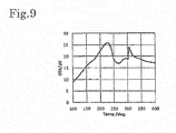
- TG-DTA was used to plot a DTA curve. Temperature was increased from 23° C to 500° C at a temperature rise rate of 10° C/min in air. The DTA curve is shown in FIG. 9 .
Landscapes
- Chemical & Material Sciences (AREA)
- Engineering & Computer Science (AREA)
- Manufacturing & Machinery (AREA)
- Mechanical Engineering (AREA)
- Composite Materials (AREA)
- Materials Engineering (AREA)
- Organic Chemistry (AREA)
- Wood Science & Technology (AREA)
- Ceramic Engineering (AREA)
- Life Sciences & Earth Sciences (AREA)
- Laminated Bodies (AREA)
- Adhesives Or Adhesive Processes (AREA)
- Powder Metallurgy (AREA)
- Structures Or Materials For Encapsulating Or Coating Semiconductor Devices Or Solid State Devices (AREA)
- Die Bonding (AREA)
Abstract
Description
- The present invention relates to a sheet and to a composite sheet.
- There are situations in which chips are secured to substrate using an electrically conductive adhesive comprising thermosetting resin (hereinafter "thermosetting adhesive"). However, there are cases in which it is not possible to ensure prescribed reliability-e.g., reliability as evaluated by temperature cycling testing-of power modules in which chips are secured to substrate using thermosetting adhesive.
- It so happens there are technologies such as those in which paste comprising nano-sized metal particles is applied to substrate and this is sintered. For example,
- Patent Reference No. 1 discloses a film comprising metal particles.
- PATENT REFERENCE NO. 1:
WO 2014/068299 A1 - It is possible that a great many organic substances will remain in the sintered body produced by sintering of the film-Example 17-disclosed at Patent Reference No. 1. This is because the film disclosed at Patent Reference No. 1 contains epoxy resin. Organic substances within the sintered body may cause reduced electrical conduction and/or reduced reliability during film temperature cycling testing.
- It is an object of the present invention to provide a sheet having a pre-sintering layer which is such that a sintered body resulting therefrom will have a small amount of remaining organic substances. It is also an object of the present invention to provide a composite sheet having a pre-sintering layer which is such that a sintered body resulting therefrom will have a small amount of remaining organic substances.
- The present invention relates to a sheet comprising a pre-sintering layer. The pre-sintering layer comprises polycarbonate. The amount of organic substances remaining in a sintered body resulting from sintering of the pre-sintering layer is likely to be less than that which would remain in a sintered body resulting from sintering of a film containing epoxy resin. This is because polycarbonate will more effectively undergo pyrolysis as a result of sintering than would be the case with epoxy resin. A sheet in accordance with the present invention is therefore more likely to excel in terms of reliability of the sintered body produced therefrom-i.e., reliability during temperature cycling testing-than would be the case with a film containing epoxy resin.
- The present invention also relates to a composite sheet. The composite sheet may comprise a release liner, a pre-sintering layer arranged over the release liner, and a dicing sheet arranged over the pre-sintering layer.
- The present invention also relates to a power module manufacturing method. A power module manufacturing method in accordance with the present invention comprises an Operation (a) in which a sheet, which comprises a dicing sheet and a pre-sintering layer arranged over the dicing sheet, is affixed to a semiconductor wafer. A power module manufacturing method in accordance with the present invention further comprises an Operation (b) in which pre-sintering chip(s), each of which comprises a semiconductor chip and pre-sintering film arranged over the semiconductor chip, are formed as a result of dicing following Operation (a). A power module manufacturing method in accordance with the present invention further comprises an Operation (c) in which pre-sintering chip(s) are compression-bonded to bonding target(s), and an Operation (d) in which sintering of pre-sintering film is carried out following Operation (c).
-
- [
FIG. 1 ] Schematic plan view of a composite sheet. - [
FIG. 2 ] Schematic sectional diagram of a portion of a composite sheet. - [
FIG. 3 ] Schematic sectional diagram showing an operation for manufacturing a power module. - [
FIG. 4 ] Schematic sectional diagram showing an operation for manufacturing a power module. - [
FIG. 5 ] Schematic sectional diagram showing an operation for manufacturing a power module. - [
FIG. 6 ] Schematic sectional diagram showing an operation for manufacturing a power module. - [
FIG. 7 ] Schematic sectional diagram of a portion of the composite sheet of Variation 4. - [
FIG. 8 ] Schematic sectional diagram showing the sheet ofVariation 5. - [
FIG. 9 ] DTA curve for Working Example 1. - Although the present invention is described in detail below in terms of embodiments, it should be understood that the present invention is not limited only to these embodiments.
- As shown in
FIG. 1 ,composite sheet 1 is in the form of a roll.Composite sheet 1 comprisesrelease liner 13 andsheets sheets 71") disposed onrelease liner 13. The distance betweensheet 71a andsheet 71b, the distance betweensheet 71b and sheet 71c, ... and the distance between sheet 71l andsheet 71m, is constant. - As shown in
FIG. 2 ,sheet 71 comprises pre-sinteringlayer 11.Sheet 71 further comprisesdicing sheet 12 arranged over pre-sinteringlayer 11.Dicing sheet 12 comprisesbase 121 andadhesive layer 122 arranged overbase 121. The two faces ofpre-sintering layer 11 may be defined such that there is a first principal plane that is in contact withadhesive layer 122 and a second principal plane that is opposite the first principal plane. The second principal plane is in contact withrelease liner 13. -
Adhesive layer 122 comprisesfirst portion 122A.First portion 122A is cured.First portion 122A is in contact withpre-sintering layer 11.Adhesive layer 122 further comprisessecond portion 122B arranged peripherally with respect tofirst portion 122A.Second portion 122B has a property such that it may be cured by means of an energy beam. As energy beam, ultraviolet beams and the like may be cited as examples.Second portion 122B is not in contact withpre-sintering layer 11. - Pre-sintering
layer 11 has a property such that it may be made into a sintered body through application of heat. Pre-sinteringlayer 11 may be used to form a joint between a first object and a second object. This might, for example, be a joint between a chip and a substrate. The base may comprise an insulator base and a conductor layer arranged over the insulator base. As insulator base, ceramic bases and so forth may be cited as examples. - It is preferred that thickness of
pre-sintering layer 11 be not less than 30 µm, and more preferred that this be not less than 40 µm. It is preferred that thickness ofpre-sintering layer 11 be not greater than 200 µm,more preferred that this be not greater than 150 µm,and still more preferred that this be not greater than 100 µm. - The DTA curve for
pre-sintering layer 11 plotted by means of TG-DTA from 23° C to 500° C at a temperature rise rate of 10° C/min in air has at least one peak between 150° C and 350° C but has no peak in the range above 350° C. When the DTA curve has a peak in the range above 350° C, this may cause a large amount of organic substances to remain following sintering. -
Pre-sintering layer 11 comprises polycarbonate. Polycarbonate may serve as binder. It is preferred that the polycarbonate be solid at 23° C. If this is solid at 23° C, it will facilitate molding ofpre-sintering layer 11. - It is preferred that the polycarbonate have a property such that it undergoes pyrolysis when sintered. For example, this may be a property such that carbon concentration is not greater than 15 wt% following an increase in temperature from 23° C to 400° C at a temperature rise rate of 10° C/min in air. Carbon concentration may be measured by means of energy dispersive x-ray analysis.
- It is preferred that the percent weight loss of polycarbonate at 300° C be greater than or equal to 95%. When this is greater than or equal to 95%, there will be a small amount of polycarbonate following sintering. It is preferred that the temperature at which the weight of polycarbonate decreases by 5% as measured by TG-DTA with temperature increasing by 10° C/min is less than or equal to 260° C. When this is less than or equal to 260° C, there will be a small amount of polycarbonate following sintering.
- It is preferred that the weight-average molecular weight of polycarbonate be not less than 10,000, more preferred that this be not less than 30,000, and still more preferred that this be not less than 50,000. It is preferred that the weight-average molecular weight of polycarbonate be not greater than 1,000,000, more preferred that this be not greater than 500,000, and still more preferred that this be not greater than 350,000. Weight-average molecular weight is measured using GPC (gel permeation chromatography) and is expressed as the polystyrene equivalent value.
- The polycarbonate might, for example, be aliphatic polycarbonate. It is preferred that the aliphatic polycarbonate be such that there are no aromatic compounds (e.g., benzene rings) between carbonate ester (-O-CO-O-) groups in the main chain. It is preferred that the aliphatic polycarbonate be such that there is/are aliphatic chain(s) between carbonate ester groups in the main chain. The aliphatic polycarbonate might, for example, be polypropylene carbonate, polyethylene carbonate, or tert-butyl ethylene carbonate. Of these, polypropylene carbonate is preferred. This is because it will effectively undergo pyrolysis when sintered.
- For every 100 wt% of
pre-sintering layer 11, it is preferred that polycarbonate be present in an amount that is not less than 0.5 wt%, and more preferred that this be not less than 1 wt%. For every 100 wt% ofpre-sintering layer 11, it is preferred that polycarbonate be present in an amount that is not greater than 20 wt%, more preferred that this be not greater than 15 wt%, still more preferred that this be not greater than 10 wt%, and even still more preferred that this be not greater than 5 wt%. -
Pre-sintering layer 11 comprises metal particles. These might be silver particles, copper particles, silver oxide particles, copper oxide particles, and/or the like.Pre-sintering layer 11 may comprise a single type of metal particles or it may comprise two or more types thereof. It is preferred that the metal particles have a property such that they become a sintered body when temperature is increased from 80° C to 300° C at a temperature rise rate of 1.5° C/second and is held at 300° C for 2.5 minutes. - The lower limit of the range in values for the average particle diameter of the metal particles might, for example, be 0.05 nm, 0.1 nm, or 1 nm. The upper limit of the range in values for the average particle diameter of the metal particles might, for example, be 1000 nm or 100 nm. D50 data obtained as a result of measurements in standard mode using a particle size analyzer (Microtrac HRA manufactured by Nikkiso Co., Ltd.) is taken to be the average particle diameter.
- For every 100 wt% of
pre-sintering layer 11, it is preferred that metal particles be present in an amount that is not less than 50 wt%, more preferred that this be not less than 60 wt%, and still more preferred that this be not less than 65 wt%. For every 100 wt% ofpre-sintering layer 11, it is preferred that metal particles be present in an amount that is not greater than 98 wt%, more preferred that this be not greater than 97 wt%, and still more preferred that this be not greater than 95 wt%. -
Pre-sintering layer 11 further comprises a binder that has a boiling point between 100° C and 350° C (hereinafter "low-boiling-point binder"). - A method such as one in which a varnish containing polycarbonate, metal particles, and so forth is prepared; a support body is coated with the varnish; and the varnish is dried might be employed to obtain
pre-sintering layer 11. The solvent for the varnish might, for example, be methyl ethyl ketone. - It is preferred that thickness of
adhesive layer 122 be not less than 3 µm, and more preferred that this be not less than 5 µm. It is preferred that thickness ofadhesive layer 122 be not greater than 50 µm, and more preferred that this be not greater than 30 µm. -
Adhesive layer 122 is formed from adhesive. The adhesive might, for example, acrylic adhesive and/or rubber-type adhesive. Of these, acrylic adhesive is preferred. The acrylic adhesive might, for example, be an acrylic adhesive in which the base polymer thereof is an acrylic polymer (homopolymer or copolymer) employing one, two, or more varieties of (meth)acrylic acid alkyl ester as monomer component(s). - It is preferred that thickness of
base 121 be 50 µm to 150 µm. It is preferred thatbase 121 have a property such that an energy beam is transmitted therethrough. - It is preferred that thickness of
release liner 13 be 20 µm to 75 µm, and more preferred that this be 25 µm to 50 µm. Asrelease liner 13, polyethylene terephthalate (PET) film and the like may be cited as examples. - As shown in
FIG. 3 ,sheet 71 is affixed to semiconductor wafer 4. Semiconductor wafer 4 might, for example, be a silicon wafer, silicon carbide wafer, gallium nitride wafer, or the like. Affixing might, for example, be carried out at 70° C to 80° C. - As shown in
FIG. 4 ,pre-sintering chips 5 are formed as a result of dicing of semiconductor wafer 4.Pre-sintering chip 5 comprisessemiconductor chip 41 andpre-sintering film 111 which is arranged oversemiconductor chip 41. - Pick-up of
pre-sintering chip 5 is carried out. That is, needle(s) are used to push uppre-sintering chip 5, grab it, and remove it fromadhesive layer 122. - As shown in
FIG. 5 , pre-sinteringcomposite body 2 is obtained as a result of compression-bonding ofpre-sintering chip 5 tobonding target 6. Compression-bonding might, for example, be carried out at 80° C to 100°C. Bonding target 6 might, for example, be a substrate, lead frame, interposer, TAB film, semiconductor, or the like. Pre-sinteringcomposite body 2 comprisesbonding target 6,semiconductor chip 41, andpre-sintering film 111 which is sandwiched betweenbonding target 6 andsemiconductor chip 41. - Sintering of
pre-sintering film 111 is carried out. That is, pre-sinteringcomposite body 2 is heated while a force is applied to pre-sinteringcomposite body 2 by means of plate(s) to causepre-sintering film 111 to become a sintered body. The lower limit of the range in values for the sintering temperature might, for example, be 200° C or 250° C. The upper limit of the range in values for the sintering temperature might, for example, be 320° C or 350° C. The lower limit of the range in values for the pressure which is applied to pre-sinteringcomposite body 2 might, for example, be 1 MPa or 5 MPa. The upper limit of the range in values for the pressure which is applied to pre-sinteringcomposite body 2 might, for example, be 20 MPa or 30 MPa. - As shown in
FIG. 6 , the electrode pads ofsemiconductor chip 41 and the terminal portions ofbonding target 6 are electrically connected by means ofbonding wire 7.Bonding wire 7 might, for example, be aluminum wire, gold wire, or copper wire. - Following wire bonding,
semiconductor chips 41 are sealed withresin sealant 8. Following sealing, further heating may be carried out. This will make it possible to achieve complete curing ofresin sealant 8 where this had been insufficiently carried out. - A power module obtained in accordance with the foregoing method comprises
bonding target 6,semiconductor chip 41, and a sintered body which is sandwiched betweenbonding target 6 andsemiconductor chip 41. The power module further comprisesresin sealant 8 with whichsemiconductor chip 41 is covered. - As described above, a method for manufacturing a power module comprises Operation (a) in which
sheet 71 is affixed to semiconductor wafer 4; Operation (b) in whichpre-sintering chip 5 is formed as a result of dicing following Operation (a); Operation (c) in whichpre-sintering chip 5 is compression-bonded tobonding target 6; and Operation (d) in which sintering ofpre-sintering film 111 is carried out following Operation (c). Operation (d) comprises a step in which pre-sinteringcomposite body 2 is heated. - A method for manufacturing a power module further comprises, following Operation (d), Operation (e) comprising a step in which a joint is formed between a first end of
bonding wire 7 andsemiconductor chip 41, and a step in which a joint is formed between a second end ofbonding wire 7 andbonding target 6. A method for manufacturing a power module further comprises Operation (f) in whichsemiconductor chip 41 is sealed withresin sealant 8. -
First portion 122A ofadhesive layer 122 has a property such that it may be cured by means of an energy beam.Second portion 122B ofadhesive layer 122 also has a property such that it may be cured by means of an energy beam. A method for manufacturing a power module further comprises, following Operation (b) in whichpre-sintering chip 5 is formed, an operation in whichadhesive layer 122 is irradiated with an energy beam and pick-up ofpre-sintering chip 5 is carried out. Irradiating this with an energy beam facilitates pick-up ofpre-sintering chip 5. -
First portion 122A ofadhesive layer 122 is cured by means of an energy beam.Second portion 122B ofadhesive layer 122 is also cured by means of an energy beam. -
Pre-sintering layer 11 constitutes a multilayer structure comprising a first layer and a second layer which is arranged over the first layer. - As shown in
FIG. 7 , the entire surface of one side ofadhesive layer 122 is in contact withpre-sintering layer 11.Adhesive layer 122 has a property such that it may be cured by means of an energy beam. A method for manufacturing a power module further comprises, following Operation (b) in whichpre-sintering chip 5 is formed, an operation in whichadhesive layer 122 is irradiated with an energy beam and pick-up ofpre-sintering chip 5 is carried out. - As shown in
FIG. 8 ,sheet 171 comprisespre-sintering layer 11. The two faces ofpre-sintering layer 11 may be defined such that there is a first face and a second face opposite the first face.Sheet 171 further comprisesfirst release liner 14 arranged over the first face andsecond release liner 15 arranged over the second face - Any of
Variation 1 throughVariation 5 and/or the like may be combined as desired. - Although working examples are employed below to describe the present invention in more specific terms, it should be understood that the present invention, inasmuch as it does not go beyond the gist thereof, is not to be limited by the following working examples.
- Silver paste: ANP-1 manufactured by Applied Nanoparticle Laboratory Corporation (paste in which nano-sized silver microparticles are dispersed in binder) in which amount of solvent for adjustment of viscosity comprised thereby was adjusted as appropriate.
Solvent: Methyl ethyl ketone (MEK)
Polycarbonate: QPAC40 (polypropylene carbonate of weight-average molecular weight 50,000 to 350,000) manufactured by Empower
Acrylic polymer: MM-2002-1 manufactured by Fujikura Kasei Co., Ltd. - Respective components and solvent were placed in the agitation vessel of a hybrid mixer (HM-500 manufactured by Keyence Corporation) as listed at TABLE 1 and made to undergo agitation for 8 minutes at 2000 rpm to obtain a varnish. The varnish was used to coat mold-release-treated film (MRA38 manufactured by Mitsubishi Plastics, Inc.). This was dried for 3 minutes at 110° C to obtain a pre-sintering sheet.
- A chip was prepared that had a silicon chip of
thickness 350 µm,length 5 mm, andwidth 5 mm; a Ti film of thickness 50 nm provided at the backside of the silicon chip; and an Ag film ofthickness 100 nm provided over the Ti film. A pre-sintering sheet was affixed to the Ag film of the chip under conditions of 70° C, 0.3 MPa, and 10 mm/sec to fabricate a pre-sintering-sheet-bearing chip. The pre-sintering-sheet-bearing chip was arranged over an Ag-plated Cu substrate which had a Cu substrate of thickness 3 mm and an Ag film ofthickness 5 µm that covered the entirety of the Cu substrate. A sintering apparatus (HTM-3000 manufactured by Hakuto Co., Ltd.) was used to carry out sintering, causing a joint to be formed between the Ag-plated Cu substrate and the chip. More specifically, a joint was formed by using a flat press to apply a pressure of 10 MPa as temperature was increased from 80° C to 300° C at a temperature rise rate of 1.5° C/second, and to apply a pressure of 10 MPa as this was maintained at 300° C for 2.5 minutes. - The sample obtained as a result of formation of the joint between the Ag-plated Cu substrate and the chip was subjected to 100 cycles of temperature variation using a thermal shock test apparatus (TSE-103ES manufactured by Espec Corp.). Each cycle consisted of a first time period during which temperature was maintained at -40° C for 15 minutes and a second time period during which temperature was maintained at 200° C for 15 minutes. After 100 cycles, an ultrasonic imaging apparatus (FineSAT II manufactured by Hitachi Kenki FineTech Co., Ltd.) was used to observe the sample. A PQ-50-13: WD (frequency 50 MHz) probe was used. Area of the portion of the joint which remained in the image that was obtained (hereinafter "remaining area") was determined. Taking total area to be 100%, the fractional remaining area was calculated. Fractional remaining area was evaluated as GOOD if it was greater than or equal to 50%. This was evaluated as BAD if it was lower than 50%. Results are shown in TABLE 1.
- Silver microparticle content was determined by means of TG-DTA when temperature was increased from 23° C to 500° C at a temperature rise rate of 10° C/min. Results are shown in TABLE 1.
TABLE 1 Working Example 1 Working Example 2 Comparative Example 1 Amount Silver paste g 3 3 3 Solvent g 2.1 2.1 2.1 Polycarbonate g 0.03 0.06 - Acrylic polymer g - - 0.03 Evaluation Silver microparticle content within 100 wt% of pre-sintering sheet wt% 94.5 93.8 94.5 Polycarbonate content within 100 wt% of pre-sintering sheet wt% 1.0 2.0 - Reliability GOOD GOOD BAD - Working Examples 1 and 2, these being examples in which polycarbonate was blended therein, had better reliability during temperature variation testing than Comparative Example 1.
- Polycarbonate Evaluation
- Percent weight loss of polycarbonate at 300° C was greater than or equal to 95%. Percent weight loss was measured using TG-DTA. The temperature at which the weight of polycarbonate decreased by 5% as measured by TG-DTA with temperature increasing by 10° C/min was less than or equal to 260° C.
- Measurement samples were cut from the pre-sintering sheet of Working Example 1. TG-DTA was used to plot a DTA curve. Temperature was increased from 23° C to 500° C at a temperature rise rate of 10° C/min in air. The DTA curve is shown in
FIG. 9 . -
- 1
- Composite sheet
- 11
- Pre-sintering layer
- 12
- Dicing sheet
- 13
- Release liner
- 71
- Sheet
- 121
- Base
- 122
- Adhesive layer
- 122A
- First portion
- 122B
- Second portion
- 2
- Pre-sintering composite body
- 4
- Semiconductor wafer
- 5
- Pre-sintering chip
- 41
- Semiconductor chip
- 111
- Pre-sintering film
- 6
- Bonding target
- 7
- Bonding wire
- 8
- Resin sealant
- 171
- Sheet
- 14
- First release liner
- 15
- Second release liner
Claims (9)
- A sheet comprising a pre-sintering layer;
wherein the pre-sintering layer comprises polycarbonate. - The sheet according to claim 1 wherein a DTA curve for the pre-sintering layer plotted by TG-DTA from 23° C to 500° C at a temperature rise rate of 10° C/min in air has at least one peak between 150° C and 350° C but has no peak in a range above 350° C.
- The sheet according to claim 1 or 2 wherein the pre-sintering layer comprises metal particles.
- The sheet according to claim 3 wherein the metal particles comprise at least one species selected from among a group consisting of silver particles, copper particles, silver oxide particles, and copper oxide particles.
- The sheet according to claim 3 or 4 wherein the metal particles are present in an amount that is 50 wt% to 98 wt% per 100 wt% of the pre-sintering layer.
- The sheet according to any of claims 1 through 5 wherein the pre-sintering layer is used to form a joint between a first object and a second object.
- The sheet according to any of claims 1 through 6
wherein two faces of the pre-sintering layer are defined such that there is a first face and a second face opposite the first face; and
further comprisinga first release liner arranged over the first face; anda second release liner arranged over the second face. - The sheet according to any of claims 1 through 6 further comprising a dicing sheet arranged over the pre-sintering layer.
- A composite sheet comprising
a release liner; and
the sheet according to claim 8 arranged over the release liner.
Applications Claiming Priority (2)
| Application Number | Priority Date | Filing Date | Title |
|---|---|---|---|
| JP2015193244A JP2017066485A (en) | 2015-09-30 | 2015-09-30 | Sheet and composite sheet |
| PCT/JP2016/077833 WO2017057127A1 (en) | 2015-09-30 | 2016-09-21 | Sheet and composite sheet |
Publications (3)
| Publication Number | Publication Date |
|---|---|
| EP3357607A1 true EP3357607A1 (en) | 2018-08-08 |
| EP3357607A4 EP3357607A4 (en) | 2018-12-19 |
| EP3357607B1 EP3357607B1 (en) | 2024-05-29 |
Family
ID=58423510
Family Applications (1)
| Application Number | Title | Priority Date | Filing Date |
|---|---|---|---|
| EP16851301.8A Active EP3357607B1 (en) | 2015-09-30 | 2016-09-21 | Sheet and composite sheet |
Country Status (6)
| Country | Link |
|---|---|
| US (1) | US10888929B2 (en) |
| EP (1) | EP3357607B1 (en) |
| JP (1) | JP2017066485A (en) |
| CN (1) | CN108136503B (en) |
| TW (1) | TWI686249B (en) |
| WO (1) | WO2017057127A1 (en) |
Cited By (4)
| Publication number | Priority date | Publication date | Assignee | Title |
|---|---|---|---|---|
| EP3239258A4 (en) * | 2014-12-24 | 2017-12-20 | Nitto Denko Corporation | Sheet for thermal bonding and sheet for thermal bonding with affixed dicing tape |
| EP3509093A4 (en) * | 2016-08-31 | 2019-07-10 | Nitto Denko Corporation | SHEET FOR THERMAL BONDING, AND SHEET FOR THERMAL BOND HAVING DIE CUTTING BAND |
| EP3509092A4 (en) * | 2016-08-31 | 2019-07-10 | Nitto Denko Corporation | THERMAL BONDING SHEET, AND THERMAL BONDING SHEET PROVIDED WITH A DIE CUTTING RIBBON |
| EP4443489A1 (en) * | 2023-04-06 | 2024-10-09 | Nitto Denko Corporation | Sinter bonding sheet |
Families Citing this family (10)
| Publication number | Priority date | Publication date | Assignee | Title |
|---|---|---|---|---|
| JP2017066485A (en) | 2015-09-30 | 2017-04-06 | 日東電工株式会社 | Sheet and composite sheet |
| JP6704322B2 (en) * | 2015-09-30 | 2020-06-03 | 日東電工株式会社 | Sheets and composite sheets |
| JP6967839B2 (en) * | 2016-03-23 | 2021-11-17 | 日東電工株式会社 | Heat bonding sheet, heat bonding sheet with dicing tape, manufacturing method of bonded body, power semiconductor device |
| JP6555694B2 (en) * | 2017-04-28 | 2019-08-07 | リンテック株式会社 | Film-like fired material and film-like fired material with support sheet |
| JP6555695B2 (en) * | 2017-10-02 | 2019-08-07 | リンテック株式会社 | Film-like fired material and film-like fired material with support sheet |
| EP3618108B1 (en) | 2017-04-28 | 2022-07-06 | LINTEC Corporation | Film-shaped fired material, and film-shaped fired material with support sheet |
| CN110574157B (en) * | 2017-04-28 | 2020-09-25 | 琳得科株式会社 | Film-like fired material and film-like fired material with support sheet |
| KR20210141490A (en) * | 2019-03-15 | 2021-11-23 | 린텍 가부시키가이샤 | Manufacturing method of film-form baking material with a support sheet, a roll body, a laminated body, and an apparatus |
| KR20220044162A (en) * | 2019-08-01 | 2022-04-06 | 린텍 가부시키가이샤 | Manufacturing method of film-form baking material with a support sheet, a roll body, a laminated body, and an apparatus |
| JP2024120482A (en) * | 2023-02-24 | 2024-09-05 | 株式会社アドバンテスト | Semiconductor device and manufacturing method |
Family Cites Families (31)
| Publication number | Priority date | Publication date | Assignee | Title |
|---|---|---|---|---|
| US5413691A (en) * | 1992-12-25 | 1995-05-09 | Tokyuama Corporation | Solid electrolyte gas-sensing device |
| JP4392732B2 (en) * | 2000-02-07 | 2010-01-06 | リンテック株式会社 | Manufacturing method of semiconductor chip |
| JP2002030306A (en) * | 2000-07-10 | 2002-01-31 | Gunze Ltd | Fiber structure and manufacturing method therefor |
| KR20040077655A (en) * | 2001-10-19 | 2004-09-06 | 슈페리어 마이크로파우더스 엘엘씨 | Tape compositions for the deposition of electronic features |
| WO2006035840A1 (en) | 2004-09-29 | 2006-04-06 | Tdk Corporation | Conductive particle manufacturing method, conductive paste, and electronic component manufacturing method |
| WO2006102592A1 (en) | 2005-03-24 | 2006-09-28 | 3M Innovative Properties Company | Metallized films and articles containing the same |
| US20070000595A1 (en) * | 2005-06-29 | 2007-01-04 | Intel Corporation | Adhesive substrate and method for using |
| JP4875357B2 (en) * | 2005-12-19 | 2012-02-15 | リンテック株式会社 | Double-sided adhesive tape |
| MY148064A (en) * | 2006-10-30 | 2013-02-28 | Sumitomo Bakelite Co | Liquid resin composition, semiconductor wafer having adhesive layer, semiconductor element having adhesive layer, semiconductor package , process for manufacturing semiconductor element and process for manufacturing semiconductor package. |
| WO2009011281A1 (en) | 2007-07-19 | 2009-01-22 | Sekisui Chemical Co., Ltd. | Dicing/die bonding tape and method for manufacturing semiconductor chip |
| JP2010254763A (en) | 2009-04-22 | 2010-11-11 | Hitachi Chem Co Ltd | Adhesive composition, manufacturing method thereof, adhesive sheet using the same, integrated sheet, manufacturing method thereof, semiconductor device, and manufacturing method thereof |
| US9011570B2 (en) * | 2009-07-30 | 2015-04-21 | Lockheed Martin Corporation | Articles containing copper nanoparticles and methods for production and use thereof |
| JP5244072B2 (en) | 2009-10-30 | 2013-07-24 | 日東電工株式会社 | Adhesive sheet with release liner |
| EP2610023B1 (en) | 2010-08-27 | 2017-09-27 | DOWA Electronics Materials Co., Ltd. | Low-temperature sinterable silver nanoparticle composition and electronic component formed using that composition |
| KR102011523B1 (en) | 2011-03-18 | 2019-08-16 | 스미토모 세이카 가부시키가이샤 | Metal paste composition |
| JP5088761B1 (en) * | 2011-11-14 | 2012-12-05 | 石原薬品株式会社 | Copper fine particle dispersion, conductive film forming method, and circuit board |
| JP5942466B2 (en) * | 2012-02-22 | 2016-06-29 | 住友金属鉱山株式会社 | Composite tungsten oxide fine particle dispersed polycarbonate resin composition, heat ray shielding molded article and heat ray shielding laminate using the same |
| KR102284082B1 (en) * | 2012-10-29 | 2021-07-30 | 알파 어셈블리 솔루션스 인크. | Sintering powder |
| GB201300538D0 (en) | 2013-01-11 | 2013-02-27 | Norner As | Polycarbonates |
| JP6542504B2 (en) | 2013-02-20 | 2019-07-10 | 日東電工株式会社 | Film adhesive, dicing tape with film adhesive, method of manufacturing semiconductor device, and semiconductor device |
| EP2960930A4 (en) | 2013-02-22 | 2017-07-12 | Furukawa Electric Co., Ltd. | Connecting structure, and semiconductor device |
| KR20140142675A (en) | 2013-06-04 | 2014-12-12 | 닛토덴코 가부시키가이샤 | Thermosetting die-bonding film, die-bonding film with dicing sheet, and process for producing semiconductor device |
| JP6118192B2 (en) | 2013-06-21 | 2017-04-19 | Dowaエレクトロニクス株式会社 | Bonding material and bonding method using the same |
| WO2015034579A1 (en) * | 2013-09-05 | 2015-03-12 | Henkel IP & Holding GmbH | Metal sintering film compositions |
| JP6245933B2 (en) | 2013-10-17 | 2017-12-13 | Dowaエレクトロニクス株式会社 | Silver sheet for bonding, method for manufacturing the same, and method for bonding electronic parts |
| WO2015060346A1 (en) | 2013-10-23 | 2015-04-30 | 日立化成株式会社 | Die bond sheet and method for manufacturing semiconductor device |
| JP2015103649A (en) * | 2013-11-25 | 2015-06-04 | 日東電工株式会社 | Thermosetting die bond film, die bond film with dicing sheet, method for manufacturing semiconductor device and semiconductor device |
| JP6682235B2 (en) | 2014-12-24 | 2020-04-15 | 日東電工株式会社 | Heat bonding sheet and heat bonding sheet with dicing tape |
| KR102270299B1 (en) * | 2015-03-02 | 2021-06-28 | 고꾸리쯔 다이가꾸호우징 도쿄노우코우다이가쿠 | Thermally decomposable binder |
| EP3294799B1 (en) * | 2015-05-08 | 2024-09-04 | Henkel AG & Co. KGaA | Sinterable films and pastes and methods for the use thereof |
| JP2017066485A (en) | 2015-09-30 | 2017-04-06 | 日東電工株式会社 | Sheet and composite sheet |
-
2015
- 2015-09-30 JP JP2015193244A patent/JP2017066485A/en active Pending
-
2016
- 2016-09-21 WO PCT/JP2016/077833 patent/WO2017057127A1/en not_active Ceased
- 2016-09-21 US US15/762,504 patent/US10888929B2/en active Active
- 2016-09-21 CN CN201680058259.9A patent/CN108136503B/en active Active
- 2016-09-21 EP EP16851301.8A patent/EP3357607B1/en active Active
- 2016-09-30 TW TW105131686A patent/TWI686249B/en active
Cited By (6)
| Publication number | Priority date | Publication date | Assignee | Title |
|---|---|---|---|---|
| EP3239258A4 (en) * | 2014-12-24 | 2017-12-20 | Nitto Denko Corporation | Sheet for thermal bonding and sheet for thermal bonding with affixed dicing tape |
| EP3509093A4 (en) * | 2016-08-31 | 2019-07-10 | Nitto Denko Corporation | SHEET FOR THERMAL BONDING, AND SHEET FOR THERMAL BOND HAVING DIE CUTTING BAND |
| EP3509092A4 (en) * | 2016-08-31 | 2019-07-10 | Nitto Denko Corporation | THERMAL BONDING SHEET, AND THERMAL BONDING SHEET PROVIDED WITH A DIE CUTTING RIBBON |
| US11390777B2 (en) | 2016-08-31 | 2022-07-19 | Nitto Denko Corporation | Sheet for heat bonding and sheet for heat bonding having dicing tape |
| US11786966B2 (en) | 2016-08-31 | 2023-10-17 | Nitto Denko Corporation | Sheet for heat bonding, and sheet for heat bonding having dicing tape |
| EP4443489A1 (en) * | 2023-04-06 | 2024-10-09 | Nitto Denko Corporation | Sinter bonding sheet |
Also Published As
| Publication number | Publication date |
|---|---|
| US10888929B2 (en) | 2021-01-12 |
| WO2017057127A1 (en) | 2017-04-06 |
| TW201713430A (en) | 2017-04-16 |
| EP3357607A4 (en) | 2018-12-19 |
| CN108136503B (en) | 2021-05-11 |
| CN108136503A (en) | 2018-06-08 |
| TWI686249B (en) | 2020-03-01 |
| EP3357607B1 (en) | 2024-05-29 |
| JP2017066485A (en) | 2017-04-06 |
| US20180257142A1 (en) | 2018-09-13 |
Similar Documents
| Publication | Publication Date | Title |
|---|---|---|
| EP3357607B1 (en) | Sheet and composite sheet | |
| EP3358609B1 (en) | Sheet and composite sheet | |
| CN110476233B (en) | Heat bonding sheet and cutting tape with heat bonding sheet | |
| EP3434398B1 (en) | Thermal bonding sheet, thermal bonding sheet with dicing tape, bonded body production method, and power semiconductor device | |
| CN108352437B (en) | Method for manufacturing semiconductor device | |
| EP3358607B1 (en) | Thermal bonding sheet, and thermal bonding sheet with dicing tape | |
| TWI845487B (en) | Composition for sintering, sheet for sintering, and dicing tape with sheet for sintering | |
| CN108174617B (en) | Heat-bonding sheet and heat-bonding sheet with dicing tape | |
| EP3358606A1 (en) | Thermal bonding sheet, and thermal bonding sheet with dicing tape | |
| CN111500212A (en) | Film-like adhesive, dicing tape-integrated film-like adhesive, and method for manufacturing semiconductor device | |
| JP7228577B2 (en) | Semiconductor device manufacturing method | |
| JP2018049932A (en) | Heat bonding sheet and dicing tape-attached heat bonding sheet | |
| CN1348976A (en) | Binder and adhesive film | |
| WO2017057485A1 (en) | Sheet and composite sheet | |
| TWI837325B (en) | Sheet for sintering bonding and sheet for sintering bonding with base material | |
| JP2022102458A (en) | Manufacturing method of semiconductor equipment, film-like adhesive and its manufacturing method, and dicing / die bonding integrated film | |
| KR102930708B1 (en) | Film-type adhesive and its manufacturing method, dicing/die bonding integrated film and its manufacturing method, and semiconductor device and its manufacturing method | |
| CN111690338A (en) | Sheet for sinter bonding and sheet for sinter bonding with base material | |
| EP4657516A1 (en) | Conductive paste and bonding method using same | |
| WO2025070385A1 (en) | Film adhesive, dicing/die attach film, semiconductor device, and production method for same |
Legal Events
| Date | Code | Title | Description |
|---|---|---|---|
| STAA | Information on the status of an ep patent application or granted ep patent |
Free format text: STATUS: THE INTERNATIONAL PUBLICATION HAS BEEN MADE |
|
| PUAI | Public reference made under article 153(3) epc to a published international application that has entered the european phase |
Free format text: ORIGINAL CODE: 0009012 |
|
| STAA | Information on the status of an ep patent application or granted ep patent |
Free format text: STATUS: REQUEST FOR EXAMINATION WAS MADE |
|
| 17P | Request for examination filed |
Effective date: 20180426 |
|
| AK | Designated contracting states |
Kind code of ref document: A1 Designated state(s): AL AT BE BG CH CY CZ DE DK EE ES FI FR GB GR HR HU IE IS IT LI LT LU LV MC MK MT NL NO PL PT RO RS SE SI SK SM TR |
|
| AX | Request for extension of the european patent |
Extension state: BA ME |
|
| A4 | Supplementary search report drawn up and despatched |
Effective date: 20181115 |
|
| RIC1 | Information provided on ipc code assigned before grant |
Ipc: B32B 9/00 20060101ALI20181109BHEP Ipc: B32B 27/36 20060101ALI20181109BHEP Ipc: B22F 7/06 20060101ALI20181109BHEP Ipc: B22F 3/02 20060101ALI20181109BHEP Ipc: H01L 21/683 20060101ALI20181109BHEP Ipc: C09J 9/02 20060101ALI20181109BHEP Ipc: B32B 27/20 20060101ALI20181109BHEP Ipc: B22F 1/00 20060101ALI20181109BHEP Ipc: B32B 7/06 20060101ALI20181109BHEP Ipc: B22F 7/08 20060101AFI20181109BHEP |
|
| DAV | Request for validation of the european patent (deleted) | ||
| DAX | Request for extension of the european patent (deleted) | ||
| STAA | Information on the status of an ep patent application or granted ep patent |
Free format text: STATUS: EXAMINATION IS IN PROGRESS |
|
| 17Q | First examination report despatched |
Effective date: 20200929 |
|
| RIN1 | Information on inventor provided before grant (corrected) |
Inventor name: SUGO, YUKI Inventor name: KAMAKURA, NAO |
|
| REG | Reference to a national code |
Ref legal event code: R079 Ipc: B22F0001100000 Ref country code: DE Ref document number: 602016087765 Country of ref document: DE Free format text: PREVIOUS MAIN CLASS: B22F0007080000 |
|
| RIC1 | Information provided on ipc code assigned before grant |
Ipc: C08K 3/08 20060101ALN20231211BHEP Ipc: C08K 3/22 20060101ALN20231211BHEP Ipc: H01L 23/31 20060101ALN20231211BHEP Ipc: H01L 23/00 20060101ALI20231211BHEP Ipc: H01L 21/683 20060101ALI20231211BHEP Ipc: C09J 9/00 20060101ALI20231211BHEP Ipc: C09J 7/10 20180101ALI20231211BHEP Ipc: B32B 27/14 20060101ALI20231211BHEP Ipc: B32B 9/04 20060101ALI20231211BHEP Ipc: B32B 7/12 20060101ALI20231211BHEP Ipc: B32B 7/06 20060101ALI20231211BHEP Ipc: B32B 5/16 20060101ALI20231211BHEP Ipc: B22F 7/08 20060101ALI20231211BHEP Ipc: B22F 7/06 20060101ALI20231211BHEP Ipc: B22F 1/10 20220101AFI20231211BHEP |
|
| GRAP | Despatch of communication of intention to grant a patent |
Free format text: ORIGINAL CODE: EPIDOSNIGR1 |
|
| STAA | Information on the status of an ep patent application or granted ep patent |
Free format text: STATUS: GRANT OF PATENT IS INTENDED |
|
| RIC1 | Information provided on ipc code assigned before grant |
Ipc: C08K 3/08 20060101ALN20240109BHEP Ipc: C08K 3/22 20060101ALN20240109BHEP Ipc: H01L 23/31 20060101ALN20240109BHEP Ipc: H01L 23/00 20060101ALI20240109BHEP Ipc: H01L 21/683 20060101ALI20240109BHEP Ipc: C09J 9/00 20060101ALI20240109BHEP Ipc: C09J 7/10 20180101ALI20240109BHEP Ipc: B32B 27/14 20060101ALI20240109BHEP Ipc: B32B 9/04 20060101ALI20240109BHEP Ipc: B32B 7/12 20060101ALI20240109BHEP Ipc: B32B 7/06 20060101ALI20240109BHEP Ipc: B32B 5/16 20060101ALI20240109BHEP Ipc: B22F 7/08 20060101ALI20240109BHEP Ipc: B22F 7/06 20060101ALI20240109BHEP Ipc: B22F 1/10 20220101AFI20240109BHEP |
|
| INTG | Intention to grant announced |
Effective date: 20240130 |
|
| GRAS | Grant fee paid |
Free format text: ORIGINAL CODE: EPIDOSNIGR3 |
|
| GRAA | (expected) grant |
Free format text: ORIGINAL CODE: 0009210 |
|
| STAA | Information on the status of an ep patent application or granted ep patent |
Free format text: STATUS: THE PATENT HAS BEEN GRANTED |
|
| P01 | Opt-out of the competence of the unified patent court (upc) registered |
Effective date: 20240409 |
|
| AK | Designated contracting states |
Kind code of ref document: B1 Designated state(s): AL AT BE BG CH CY CZ DE DK EE ES FI FR GB GR HR HU IE IS IT LI LT LU LV MC MK MT NL NO PL PT RO RS SE SI SK SM TR |
|
| REG | Reference to a national code |
Ref country code: CH Ref legal event code: EP |
|
| REG | Reference to a national code |
Ref country code: IE Ref legal event code: FG4D |
|
| REG | Reference to a national code |
Ref country code: DE Ref legal event code: R096 Ref document number: 602016087765 Country of ref document: DE |
|
| REG | Reference to a national code |
Ref country code: LT Ref legal event code: MG9D |
|
| REG | Reference to a national code |
Ref country code: NL Ref legal event code: MP Effective date: 20240529 |
|
| PG25 | Lapsed in a contracting state [announced via postgrant information from national office to epo] |
Ref country code: IS Free format text: LAPSE BECAUSE OF FAILURE TO SUBMIT A TRANSLATION OF THE DESCRIPTION OR TO PAY THE FEE WITHIN THE PRESCRIBED TIME-LIMIT Effective date: 20240929 |
|
| PG25 | Lapsed in a contracting state [announced via postgrant information from national office to epo] |
Ref country code: BG Free format text: LAPSE BECAUSE OF FAILURE TO SUBMIT A TRANSLATION OF THE DESCRIPTION OR TO PAY THE FEE WITHIN THE PRESCRIBED TIME-LIMIT Effective date: 20240529 |
|
| PG25 | Lapsed in a contracting state [announced via postgrant information from national office to epo] |
Ref country code: HR Free format text: LAPSE BECAUSE OF FAILURE TO SUBMIT A TRANSLATION OF THE DESCRIPTION OR TO PAY THE FEE WITHIN THE PRESCRIBED TIME-LIMIT Effective date: 20240529 Ref country code: FI Free format text: LAPSE BECAUSE OF FAILURE TO SUBMIT A TRANSLATION OF THE DESCRIPTION OR TO PAY THE FEE WITHIN THE PRESCRIBED TIME-LIMIT Effective date: 20240529 |
|
| PG25 | Lapsed in a contracting state [announced via postgrant information from national office to epo] |
Ref country code: GR Free format text: LAPSE BECAUSE OF FAILURE TO SUBMIT A TRANSLATION OF THE DESCRIPTION OR TO PAY THE FEE WITHIN THE PRESCRIBED TIME-LIMIT Effective date: 20240830 |
|
| REG | Reference to a national code |
Ref country code: AT Ref legal event code: MK05 Ref document number: 1690214 Country of ref document: AT Kind code of ref document: T Effective date: 20240529 |
|
| PG25 | Lapsed in a contracting state [announced via postgrant information from national office to epo] |
Ref country code: ES Free format text: LAPSE BECAUSE OF FAILURE TO SUBMIT A TRANSLATION OF THE DESCRIPTION OR TO PAY THE FEE WITHIN THE PRESCRIBED TIME-LIMIT Effective date: 20240529 |
|
| PG25 | Lapsed in a contracting state [announced via postgrant information from national office to epo] |
Ref country code: AT Free format text: LAPSE BECAUSE OF FAILURE TO SUBMIT A TRANSLATION OF THE DESCRIPTION OR TO PAY THE FEE WITHIN THE PRESCRIBED TIME-LIMIT Effective date: 20240529 |
|
| PG25 | Lapsed in a contracting state [announced via postgrant information from national office to epo] |
Ref country code: PL Free format text: LAPSE BECAUSE OF FAILURE TO SUBMIT A TRANSLATION OF THE DESCRIPTION OR TO PAY THE FEE WITHIN THE PRESCRIBED TIME-LIMIT Effective date: 20240529 |
|
| PG25 | Lapsed in a contracting state [announced via postgrant information from national office to epo] |
Ref country code: LV Free format text: LAPSE BECAUSE OF FAILURE TO SUBMIT A TRANSLATION OF THE DESCRIPTION OR TO PAY THE FEE WITHIN THE PRESCRIBED TIME-LIMIT Effective date: 20240529 |
|
| PG25 | Lapsed in a contracting state [announced via postgrant information from national office to epo] |
Ref country code: PL Free format text: LAPSE BECAUSE OF FAILURE TO SUBMIT A TRANSLATION OF THE DESCRIPTION OR TO PAY THE FEE WITHIN THE PRESCRIBED TIME-LIMIT Effective date: 20240529 Ref country code: NO Free format text: LAPSE BECAUSE OF FAILURE TO SUBMIT A TRANSLATION OF THE DESCRIPTION OR TO PAY THE FEE WITHIN THE PRESCRIBED TIME-LIMIT Effective date: 20240829 Ref country code: LV Free format text: LAPSE BECAUSE OF FAILURE TO SUBMIT A TRANSLATION OF THE DESCRIPTION OR TO PAY THE FEE WITHIN THE PRESCRIBED TIME-LIMIT Effective date: 20240529 Ref country code: IS Free format text: LAPSE BECAUSE OF FAILURE TO SUBMIT A TRANSLATION OF THE DESCRIPTION OR TO PAY THE FEE WITHIN THE PRESCRIBED TIME-LIMIT Effective date: 20240929 Ref country code: HR Free format text: LAPSE BECAUSE OF FAILURE TO SUBMIT A TRANSLATION OF THE DESCRIPTION OR TO PAY THE FEE WITHIN THE PRESCRIBED TIME-LIMIT Effective date: 20240529 Ref country code: GR Free format text: LAPSE BECAUSE OF FAILURE TO SUBMIT A TRANSLATION OF THE DESCRIPTION OR TO PAY THE FEE WITHIN THE PRESCRIBED TIME-LIMIT Effective date: 20240830 Ref country code: FI Free format text: LAPSE BECAUSE OF FAILURE TO SUBMIT A TRANSLATION OF THE DESCRIPTION OR TO PAY THE FEE WITHIN THE PRESCRIBED TIME-LIMIT Effective date: 20240529 Ref country code: ES Free format text: LAPSE BECAUSE OF FAILURE TO SUBMIT A TRANSLATION OF THE DESCRIPTION OR TO PAY THE FEE WITHIN THE PRESCRIBED TIME-LIMIT Effective date: 20240529 Ref country code: BG Free format text: LAPSE BECAUSE OF FAILURE TO SUBMIT A TRANSLATION OF THE DESCRIPTION OR TO PAY THE FEE WITHIN THE PRESCRIBED TIME-LIMIT Effective date: 20240529 Ref country code: AT Free format text: LAPSE BECAUSE OF FAILURE TO SUBMIT A TRANSLATION OF THE DESCRIPTION OR TO PAY THE FEE WITHIN THE PRESCRIBED TIME-LIMIT Effective date: 20240529 Ref country code: RS Free format text: LAPSE BECAUSE OF FAILURE TO SUBMIT A TRANSLATION OF THE DESCRIPTION OR TO PAY THE FEE WITHIN THE PRESCRIBED TIME-LIMIT Effective date: 20240829 |
|
| PG25 | Lapsed in a contracting state [announced via postgrant information from national office to epo] |
Ref country code: NL Free format text: LAPSE BECAUSE OF FAILURE TO SUBMIT A TRANSLATION OF THE DESCRIPTION OR TO PAY THE FEE WITHIN THE PRESCRIBED TIME-LIMIT Effective date: 20240529 |
|
| PG25 | Lapsed in a contracting state [announced via postgrant information from national office to epo] |
Ref country code: NL Free format text: LAPSE BECAUSE OF FAILURE TO SUBMIT A TRANSLATION OF THE DESCRIPTION OR TO PAY THE FEE WITHIN THE PRESCRIBED TIME-LIMIT Effective date: 20240529 |
|
| PG25 | Lapsed in a contracting state [announced via postgrant information from national office to epo] |
Ref country code: DK Free format text: LAPSE BECAUSE OF FAILURE TO SUBMIT A TRANSLATION OF THE DESCRIPTION OR TO PAY THE FEE WITHIN THE PRESCRIBED TIME-LIMIT Effective date: 20240529 |
|
| PG25 | Lapsed in a contracting state [announced via postgrant information from national office to epo] |
Ref country code: EE Free format text: LAPSE BECAUSE OF FAILURE TO SUBMIT A TRANSLATION OF THE DESCRIPTION OR TO PAY THE FEE WITHIN THE PRESCRIBED TIME-LIMIT Effective date: 20240529 |
|
| PG25 | Lapsed in a contracting state [announced via postgrant information from national office to epo] |
Ref country code: CZ Free format text: LAPSE BECAUSE OF FAILURE TO SUBMIT A TRANSLATION OF THE DESCRIPTION OR TO PAY THE FEE WITHIN THE PRESCRIBED TIME-LIMIT Effective date: 20240529 |
|
| PG25 | Lapsed in a contracting state [announced via postgrant information from national office to epo] |
Ref country code: SK Free format text: LAPSE BECAUSE OF FAILURE TO SUBMIT A TRANSLATION OF THE DESCRIPTION OR TO PAY THE FEE WITHIN THE PRESCRIBED TIME-LIMIT Effective date: 20240529 Ref country code: RO Free format text: LAPSE BECAUSE OF FAILURE TO SUBMIT A TRANSLATION OF THE DESCRIPTION OR TO PAY THE FEE WITHIN THE PRESCRIBED TIME-LIMIT Effective date: 20240529 |
|
| PG25 | Lapsed in a contracting state [announced via postgrant information from national office to epo] |
Ref country code: SM Free format text: LAPSE BECAUSE OF FAILURE TO SUBMIT A TRANSLATION OF THE DESCRIPTION OR TO PAY THE FEE WITHIN THE PRESCRIBED TIME-LIMIT Effective date: 20240529 |
|
| PG25 | Lapsed in a contracting state [announced via postgrant information from national office to epo] |
Ref country code: SM Free format text: LAPSE BECAUSE OF FAILURE TO SUBMIT A TRANSLATION OF THE DESCRIPTION OR TO PAY THE FEE WITHIN THE PRESCRIBED TIME-LIMIT Effective date: 20240529 Ref country code: SK Free format text: LAPSE BECAUSE OF FAILURE TO SUBMIT A TRANSLATION OF THE DESCRIPTION OR TO PAY THE FEE WITHIN THE PRESCRIBED TIME-LIMIT Effective date: 20240529 Ref country code: RO Free format text: LAPSE BECAUSE OF FAILURE TO SUBMIT A TRANSLATION OF THE DESCRIPTION OR TO PAY THE FEE WITHIN THE PRESCRIBED TIME-LIMIT Effective date: 20240529 Ref country code: EE Free format text: LAPSE BECAUSE OF FAILURE TO SUBMIT A TRANSLATION OF THE DESCRIPTION OR TO PAY THE FEE WITHIN THE PRESCRIBED TIME-LIMIT Effective date: 20240529 Ref country code: DK Free format text: LAPSE BECAUSE OF FAILURE TO SUBMIT A TRANSLATION OF THE DESCRIPTION OR TO PAY THE FEE WITHIN THE PRESCRIBED TIME-LIMIT Effective date: 20240529 Ref country code: CZ Free format text: LAPSE BECAUSE OF FAILURE TO SUBMIT A TRANSLATION OF THE DESCRIPTION OR TO PAY THE FEE WITHIN THE PRESCRIBED TIME-LIMIT Effective date: 20240529 |
|
| REG | Reference to a national code |
Ref country code: DE Ref legal event code: R097 Ref document number: 602016087765 Country of ref document: DE |
|
| PLBE | No opposition filed within time limit |
Free format text: ORIGINAL CODE: 0009261 |
|
| STAA | Information on the status of an ep patent application or granted ep patent |
Free format text: STATUS: NO OPPOSITION FILED WITHIN TIME LIMIT |
|
| PG25 | Lapsed in a contracting state [announced via postgrant information from national office to epo] |
Ref country code: MC Free format text: LAPSE BECAUSE OF FAILURE TO SUBMIT A TRANSLATION OF THE DESCRIPTION OR TO PAY THE FEE WITHIN THE PRESCRIBED TIME-LIMIT Effective date: 20240529 Ref country code: SI Free format text: LAPSE BECAUSE OF FAILURE TO SUBMIT A TRANSLATION OF THE DESCRIPTION OR TO PAY THE FEE WITHIN THE PRESCRIBED TIME-LIMIT Effective date: 20240529 |
|
| REG | Reference to a national code |
Ref country code: CH Ref legal event code: PL |
|
| 26N | No opposition filed |
Effective date: 20250303 |
|
| PG25 | Lapsed in a contracting state [announced via postgrant information from national office to epo] |
Ref country code: LU Free format text: LAPSE BECAUSE OF NON-PAYMENT OF DUE FEES Effective date: 20240921 |
|
| GBPC | Gb: european patent ceased through non-payment of renewal fee |
Effective date: 20240921 |
|
| PG25 | Lapsed in a contracting state [announced via postgrant information from national office to epo] |
Ref country code: GB Free format text: LAPSE BECAUSE OF NON-PAYMENT OF DUE FEES Effective date: 20240921 |
|
| REG | Reference to a national code |
Ref country code: BE Ref legal event code: MM Effective date: 20240930 |
|
| PG25 | Lapsed in a contracting state [announced via postgrant information from national office to epo] |
Ref country code: BE Free format text: LAPSE BECAUSE OF NON-PAYMENT OF DUE FEES Effective date: 20240930 |
|
| PG25 | Lapsed in a contracting state [announced via postgrant information from national office to epo] |
Ref country code: FR Free format text: LAPSE BECAUSE OF NON-PAYMENT OF DUE FEES Effective date: 20240930 |
|
| PG25 | Lapsed in a contracting state [announced via postgrant information from national office to epo] |
Ref country code: CH Free format text: LAPSE BECAUSE OF NON-PAYMENT OF DUE FEES Effective date: 20240930 |
|
| PG25 | Lapsed in a contracting state [announced via postgrant information from national office to epo] |
Ref country code: IE Free format text: LAPSE BECAUSE OF NON-PAYMENT OF DUE FEES Effective date: 20240921 |
|
| PG25 | Lapsed in a contracting state [announced via postgrant information from national office to epo] |
Ref country code: SE Free format text: LAPSE BECAUSE OF FAILURE TO SUBMIT A TRANSLATION OF THE DESCRIPTION OR TO PAY THE FEE WITHIN THE PRESCRIBED TIME-LIMIT Effective date: 20240529 |
|
| PGFP | Annual fee paid to national office [announced via postgrant information from national office to epo] |
Ref country code: DE Payment date: 20250730 Year of fee payment: 10 |
|
| PGFP | Annual fee paid to national office [announced via postgrant information from national office to epo] |
Ref country code: IT Payment date: 20250825 Year of fee payment: 10 |
|
| PG25 | Lapsed in a contracting state [announced via postgrant information from national office to epo] |
Ref country code: PT Free format text: LAPSE BECAUSE OF NON-PAYMENT OF DUE FEES Effective date: 20240529 |
|
| PG25 | Lapsed in a contracting state [announced via postgrant information from national office to epo] |
Ref country code: CY Free format text: LAPSE BECAUSE OF FAILURE TO SUBMIT A TRANSLATION OF THE DESCRIPTION OR TO PAY THE FEE WITHIN THE PRESCRIBED TIME-LIMIT; INVALID AB INITIO Effective date: 20160921 |
|
| PG25 | Lapsed in a contracting state [announced via postgrant information from national office to epo] |
Ref country code: HU Free format text: LAPSE BECAUSE OF FAILURE TO SUBMIT A TRANSLATION OF THE DESCRIPTION OR TO PAY THE FEE WITHIN THE PRESCRIBED TIME-LIMIT; INVALID AB INITIO Effective date: 20160921 |