EP3355473A1 - Level shifter - Google Patents
Level shifter Download PDFInfo
- Publication number
- EP3355473A1 EP3355473A1 EP18150031.5A EP18150031A EP3355473A1 EP 3355473 A1 EP3355473 A1 EP 3355473A1 EP 18150031 A EP18150031 A EP 18150031A EP 3355473 A1 EP3355473 A1 EP 3355473A1
- Authority
- EP
- European Patent Office
- Prior art keywords
- transistor
- power supply
- voltage signal
- main electrode
- level shifter
- Prior art date
- Legal status (The legal status is an assumption and is not a legal conclusion. Google has not performed a legal analysis and makes no representation as to the accuracy of the status listed.)
- Granted
Links
Images


Classifications
-
- H—ELECTRICITY
- H03—ELECTRONIC CIRCUITRY
- H03K—PULSE TECHNIQUE
- H03K19/00—Logic circuits, i.e. having at least two inputs acting on one output; Inverting circuits
- H03K19/0175—Coupling arrangements; Interface arrangements
- H03K19/0185—Coupling arrangements; Interface arrangements using field effect transistors only
- H03K19/018507—Interface arrangements
- H03K19/018521—Interface arrangements of complementary type, e.g. CMOS
-
- H—ELECTRICITY
- H03—ELECTRONIC CIRCUITRY
- H03K—PULSE TECHNIQUE
- H03K19/00—Logic circuits, i.e. having at least two inputs acting on one output; Inverting circuits
- H03K19/0175—Coupling arrangements; Interface arrangements
- H03K19/0185—Coupling arrangements; Interface arrangements using field effect transistors only
- H03K19/018507—Interface arrangements
-
- H—ELECTRICITY
- H03—ELECTRONIC CIRCUITRY
- H03K—PULSE TECHNIQUE
- H03K19/00—Logic circuits, i.e. having at least two inputs acting on one output; Inverting circuits
- H03K19/0175—Coupling arrangements; Interface arrangements
- H03K19/017509—Interface arrangements
-
- H—ELECTRICITY
- H03—ELECTRONIC CIRCUITRY
- H03K—PULSE TECHNIQUE
- H03K3/00—Circuits for generating electric pulses; Monostable, bistable or multistable circuits
- H03K3/02—Generators characterised by the type of circuit or by the means used for producing pulses
- H03K3/353—Generators characterised by the type of circuit or by the means used for producing pulses by the use, as active elements, of field-effect transistors with internal or external positive feedback
- H03K3/356—Bistable circuits
- H03K3/356017—Bistable circuits using additional transistors in the input circuit
- H03K3/356052—Bistable circuits using additional transistors in the input circuit using pass gates
-
- H—ELECTRICITY
- H10—SEMICONDUCTOR DEVICES; ELECTRIC SOLID-STATE DEVICES NOT OTHERWISE PROVIDED FOR
- H10D—INORGANIC ELECTRIC SEMICONDUCTOR DEVICES
- H10D89/00—Aspects of integrated devices not covered by groups H10D84/00 - H10D88/00
- H10D89/60—Integrated devices comprising arrangements for electrical or thermal protection, e.g. protection circuits against electrostatic discharge [ESD]
- H10D89/601—Integrated devices comprising arrangements for electrical or thermal protection, e.g. protection circuits against electrostatic discharge [ESD] for devices having insulated gate electrodes, e.g. for IGFETs or IGBTs
- H10D89/911—Integrated devices comprising arrangements for electrical or thermal protection, e.g. protection circuits against electrostatic discharge [ESD] for devices having insulated gate electrodes, e.g. for IGFETs or IGBTs using passive elements as protective elements
-
- H—ELECTRICITY
- H02—GENERATION; CONVERSION OR DISTRIBUTION OF ELECTRIC POWER
- H02H—EMERGENCY PROTECTIVE CIRCUIT ARRANGEMENTS
- H02H9/00—Emergency protective circuit arrangements for limiting excess current or voltage without disconnection
- H02H9/04—Emergency protective circuit arrangements for limiting excess current or voltage without disconnection responsive to excess voltage
- H02H9/045—Emergency protective circuit arrangements for limiting excess current or voltage without disconnection responsive to excess voltage adapted to a particular application and not provided for elsewhere
- H02H9/046—Emergency protective circuit arrangements for limiting excess current or voltage without disconnection responsive to excess voltage adapted to a particular application and not provided for elsewhere responsive to excess voltage appearing at terminals of integrated circuits
Definitions
- the present invention relates to a level shifter.
- Japanese Patent No. 5,465,548 discloses a level shifter that converts a high voltage supplied from an in-vehicle battery to a low voltage that is usable in an engine control unit (ECU) and the like.
- This level shifter includes a level shift section.
- the level shift section inputs an input voltage signal and outputs an output voltage signal that is level-shifted from the high voltage to the low voltage.
- This level shifter has a circuit configuration in which the voltage level of a threshold voltage of the input voltage signal is constant, even if the voltage level of the high voltage supplied from the in-vehicle battery changes.
- the threshold voltage When, for example, there is a voltage drop at the in-vehicle battery, then if the threshold voltage is constant, the input voltage signal at the high level may not actually reach the threshold voltage and may be judged to be at a low level. Thus, misoperation may occur. Accordingly, there are calls for a level shifter in which the threshold voltage of an input voltage signal is changed in accordance with voltage changes.
- the present disclosure provides a level shifter in which a threshold voltage of an input voltage signal may be changed in accordance with a change in a power supply voltage.
- a level shifter includes: a power supply system current source including: a first resistor having a first end that is connected to a first power supply voltage, and having a second end, and a first transistor having a first main electrode and a first control electrode that are connected to the second end of the first resistor, and having a second main electrode that is connected to a second power supply voltage having a lower voltage than the first power supply voltage; a second transistor having a third main electrode that is connected to an input voltage signal terminal, a fourth main electrode that is connected to an output voltage signal terminal, and a second control electrode that is connected to a third power supply voltage having a voltage that is lower than the first power supply voltage and higher than the second power supply voltage; a second resistor having a first end that is connected between the fourth main electrode and the output voltage signal terminal, and having a second end; and a third transistor having a fifth main electrode that is connected to the second end of the second resistor, a sixth main electrode that is connected to the second power supply voltage
- the level shifter according to the first aspect is provided with the power supply system current source, the second transistor, the second resistor and the third transistor.
- the power supply system current source includes the first resistor and the first transistor. The one end of the first resistor is connected to the first power supply voltage.
- the first main electrode and first control electrode of the first transistor is connected to the other end of the first resistor, and the second main electrode of the first transistor is connected to the second power supply voltage.
- the second power supply voltage is a voltage lower than the first power supply voltage.
- the third main electrode of the second transistor is connected to the input voltage signal terminal, and the fourth main electrode of the second transistor is connected to the output voltage signal terminal.
- the second control electrode of the second transistor is connected to the third power supply voltage.
- the third power supply voltage is a voltage lower than the first power supply voltage but higher than the second power supply voltage.
- the one end of the second resistor is connected to between the fourth main electrode of the second transistor and the output voltage signal terminal.
- the fifth main electrode of the third transistor is connected to the other end of the second resistor, and the sixth main electrode of the third transistor is connected to the second power supply voltage.
- the third control electrode of the third transistor is connected to the first control electrode of the first transistor.
- the third transistor constitutes a current mirror circuit with the power supply system current source (the first transistor).
- the power supply system current source implements current regulation.
- the input voltage signal passes through the second transistor, the second resistor and the third transistor, and is outputted to the second power supply voltage as a current.
- the current flowing in the third transistor constituting the current mirror circuit is regulated in accordance with changes in the current flowing in the first transistor of the power supply system current source.
- the voltage level of a threshold voltage of the input voltage signal may be changed.
- an electrostatic protection component is disposed between the input voltage signal terminal and the third main electrode of the second transistor.
- the electrostatic protection component is disposed between the input voltage signal terminal and the second transistor, electrostatic breakdown of the second transistor may be prevented or effectively suppressed. Therefore, electrostatic breakdown endurance of the level shifter may be improved.
- an electrostatic breakdown voltage of the second transistor is higher than respective electrostatic breakdown voltages of the first transistor and the third transistor.
- the electrostatic breakdown voltage of the second transistor is specified to be higher, electrostatic breakdown of the second transistor may be prevented or effectively suppressed. Therefore, electrostatic breakdown endurance of the level shifter may be improved.
- the second transistor includes a vertical diffused-type transistor.
- the second transistor is a vertical diffused-type transistor
- the electrostatic breakdown voltage of the second transistor may be improved. Therefore, electrostatic breakdown endurance of the level shifter may be improved.
- the level shifter according to any one of the first to fourth aspects, further includes a buffer section that shapes a waveform of an output voltage signal and that is connected to the output voltage signal terminal.
- the waveform of an output voltage signal that is outputted from the output voltage signal terminal may be shaped using the buffer section, and ultimately the shaped output voltage signal may be outputted.
- the level shifter according to the present disclosure provides an excellent effect in that a threshold voltage of an input voltage signal may be changed in accordance with a change in a power supply voltage.
- a level shifter according to an exemplary embodiment of the present disclosure is described below using Fig. 1 to Fig. 4 .
- structural elements that have the same functions or substantially the same functions are assigned the same reference symbols, and duplicative descriptions are omitted.
- a level shifter 1 is driven by a first power supply voltage V BB with a high voltage that is supplied from an in-vehicle battery.
- the level shifter 1 is structured with a level shift section 2 and a buffer section 3.
- the level shifter 1 outputs an output voltage signal S OUT1 and an inverted output voltage signal S OUT2 , which are level-shifted from the first power supply voltage V BB to a lower voltage in accordance with an input voltage signal S IN at lower voltages than the first power supply voltage V BB .
- the input voltage signal S IN is applied to an input voltage signal terminal S1 of the level shifter 1.
- the output voltage signal S OUT1 is outputted to an output voltage signal terminal S3, and the output voltage signal S OUT2 is outputted to an output voltage signal terminal S4.
- the first power supply voltage V BB is, for example, between 8 V and 18 V.
- the input voltage signal S IN is, for example, a rising signal from 0 V (low level) to 6 V (high level) or a falling signal from 6 V to 0 V.
- the output voltage signal S OUT1 is, for example, a rising signal from 0 V (low level) to 5 V (high level) or a falling signal from 5 V to 0 V.
- the inverted output voltage signal S OUT2 is an inverted voltage signal of the output voltage signal S OUT1 .
- a second power supply voltage Vss is 0 V.
- the level shift section 2 of the level shifter 1 includes a power supply system current source 20, a second transistor T2, a second resistor R2 and a third transistor T3.
- the power supply system current source 20 is provided with a first resistor R1 and a first transistor T1.
- An electrostatic protection component is disposed at the level shift section 2.
- the electrostatic protection component is structured by a third resistor R3.
- one end of the first resistor R1 of the power supply system current source 20 is connected to the first power supply voltage V BB .
- the first transistor T1 is structured by an insulated gate field-effect transistor (IGFET) of the n-channel conduction type, which serves as a first conduction type in the present exemplary embodiment.
- IGFETs include at least metal-oxide-semiconductor (MOS)FETs and metal-insulator-semiconductor (MIS)FETs.
- MOS metal-oxide-semiconductor
- MIS metal-insulator-semiconductor
- a first main electrode (the drain electrode) of the first transistor T1 is connected to the other end of the first resistor R1, and a second main electrode (the source electrode) of the first transistor T1 is connected to the second power supply voltage V SS .
- a first control electrode (the gate electrode) of the first transistor T1 is connected to both the first resistor R1 and a third control electrode (the gate electrode) of the third transistor T3.
- the second transistor T2 is structured by a high-breakdown-voltage transistor with a higher electrostatic breakdown voltage than an electrostatic breakdown voltage of the first transistor T1.
- the second transistor T2 is structured by a vertical diffused metal-oxide-semiconductor field effect transistor (VDMOSFET). This second transistor T2 may simply be referred to as a VDMOSFET or a vertical diffused-type transistor).
- the second transistor T2 is specified to be of the first conduction type.
- a third main electrode (the drain electrode) of the second transistor T2 is connected to the input voltage signal terminal S1, and a fourth main electrode (the source electrode) of the second transistor T2 is connected to an output voltage signal terminal S2 of the level shift section 2.
- An output signal voltage S OUT in which the high voltage of the first power supply voltage V BB has been level-shifted to a low voltage is outputted at the output voltage signal terminal S2.
- a second control electrode (the gate electrode) of the second transistor T2 is connected to a third power supply voltage V CC .
- This third power supply voltage V CC is a voltage that is lower than the first power supply voltage V BB but higher than the second power supply voltage V SS , specifically being 5 V.
- the second transistor T2 acts as a clamp transistor that does not output signals above a certain voltage to the output voltage signal terminal S2.
- One end of the second resistor R2 is connected to between the fourth main electrode of the second transistor T2 and the output voltage signal terminal S2.
- the second resistor R2 is used for regulation of a threshold voltage of the input voltage signal S IN .
- the third transistor T3 is structured by an IGFET of the first conduction type, which is constituted with a similar structure to the first transistor T1.
- a fifth main electrode (the drain electrode) of the third transistor is connected to the other end of the second resistor R2, and a sixth main electrode (the source electrode) of the third transistor T3 is connected to the second power supply voltage V SS .
- the third control electrode is connected to the first control electrode of the first transistor T1. Therefore, the third transistor T3 constitutes a current mirror circuit with the first transistor T1.
- the third resistor R3 serves as the electrostatic protection component.
- One end of the third resistor R3 is connected to the input voltage signal terminal S1, and the other end is connected to the third main electrode of the second transistor T2.
- the electrostatic protection component is structured by the third resistor R3 in the present exemplary embodiment, the electrostatic protection component may be structured in the present exemplary embodiment by using a reverse-connected diode or combining a diode and a resistor.
- the buffer section 3 of the level shifter 1 includes three stages that are electrically connected in series: a first inverter 30, a second inverter 31 and a third inverter 32.
- the first inverter 30 includes a fourth transistor T4 and a fifth transistor T5.
- the fourth transistor T4 is structured by an IGFET of the first conduction type.
- One main electrode of the fourth transistor T4, which is the source electrode, is connected to the second power supply voltage V SS .
- the other main electrode of the fourth transistor T4, which is the drain electrode, is connected to the other main electrode of the fifth transistor T5, which is the drain electrode thereof, and to gate electrodes of the second inverter 31.
- the gate electrode of the fourth transistor T4 is connected to the output voltage signal terminal S2.
- the fifth transistor is structured by an IGFET of the p-channel conduction type, which serves as a second conduction type.
- One main electrode of the fifth transistor T5, which is the source electrode, is connected to the third power supply voltage V CC .
- the drain electrode of the fifth transistor T5 is connected to the drain electrode of the fourth transistor T4 and to the gate electrodes of the second inverter 31.
- the gate electrode of the fifth transistor T5 is connected to the output voltage signal terminal S2.
- the first inverter 30 shapes a waveform of the output voltage signal S OUT that is outputted from the output voltage signal terminal S2.
- the second inverter 31 is arranged as a circuit succeeding the first inverter 30, and includes a sixth transistor T6 and a seventh transistor T7.
- the sixth transistor T6 is constituted with a similar structure to the fourth transistor T4, and the seventh transistor T7 is constituted with a similar constituted to the fifth transistor T5.
- the gate electrodes of the sixth transistor T6 and the seventh transistor T7 are connected to the first inverter 30.
- the drain electrodes of the sixth transistor T6 and the seventh transistor T7 are connected to the third inverter 32 and to an output voltage signal terminal S4.
- the inverted output voltage signal S OUT2 is outputted at the output voltage signal terminal S4.
- the third inverter 32 is arranged as a circuit succeeding the second inverter 31, and includes an eighth transistor T8 and a ninth transistor T9.
- the eighth transistor T8 is constituted with a similar structure to the fourth transistor T4, and the ninth transistor T9 is constituted with a similar structure to the fifth transistor T5.
- the gate electrodes of the eighth transistor T8 and the ninth transistor T9 are connected to the second inverter 31.
- the drain electrodes of the eighth transistor T8 and the ninth transistor T9 are connected to the output voltage signal terminal S3.
- the output voltage signal S OUT1 is outputted at the output voltage signal terminal S3.
- the level shifter 1 is structured as a semiconductor integrated circuit (a semiconductor device). As illustrated in Fig. 2 and Fig. 3 , the level shifter 1 is formed with a semiconductor substrate 40 serving as a base. In the present exemplary embodiment, an n-type silicon monocrystalline substrate is employed for the semiconductor substrate 40.
- the respective semiconductor components are formed within a region of the epitaxial growth layer 41 whose periphery is encircled by a component isolation region 42.
- the first resistor R1 is formed by a second conduction type (p-type) semiconductor region 47 disposed in a principal surface portion of a first conduction type (n-type) well region 43 that is formed in the epitaxial growth layer 41.
- the second resistor R2 and the third resistor R3 are structured with similar vertical cross-section structures to the first resistor R1.
- the first transistor T1 is disposed in a principal surface portion of a second conduction type well region 44 that is formed in the epitaxial growth layer 41.
- the first transistor T1 is structured with a channel formation region formed by the well region 44, a pair of first conduction type semiconductor regions 48 to be used as the first main electrode and the second main electrode, a gate isolation layer 50, and a gate electrode 51 to serve as the first control electrode.
- the pair of semiconductor regions 48 are formed in principal surface portions of the well region 44 that are separated from one another with the channel formation region therebetween.
- the gate isolation layer 50 is formed on the channel formation region (on the principal surface of the well region 44).
- the gate electrode 51 is formed on the gate isolation layer 50.
- the third transistor T3 is structured with a similar vertical cross-section structure to the first transistor T1.
- the second transistor T2 is structured by a VDMOSFET in the present exemplary embodiment.
- the second transistor T2 is structured with the third main electrode, a channel formation region, the fourth main electrode, another of the gate isolation layer 50, and another of the gate electrode 51 to serve as the second control electrode.
- the third main electrode is structured with another of the well region 43.
- An impurity density of the well region 43 is specified to be lower than the impurity densities of the semiconductor substrate 40 and the semiconductor region 48.
- the channel formation region is formed at principal surface portions of second conduction type base regions 45 that are formed in principal surface portions of the well region 43 at end portions of the gate electrode 51.
- the base regions 45 connect with second conduction type semiconductor regions 46 with higher impurity densities than the base regions 45.
- the fourth main electrode is formed by another of the semiconductor region 48 that is formed at a principal surface portion of the base regions 45.
- the impurity density of the semiconductor region 48 is specified to be higher than the impurity density of the semiconductor substrate 40.
- the gate isolation layer 50 is formed on the channel formation region (on the principal surface of the base regions 45), and the gate electrode 51 is formed on the gate isolation layer 50.
- the fourth transistor T4 of the first inverter 30 of the buffer section 3 is formed at the principal surface portion of the well region 44 within a region whose periphery is encircled by the component isolation region 42.
- the fourth transistor T4 is structured with another of the well region 44 to serve as a channel formation region, another pair of the semiconductor regions 48 to serve as the one main electrode and the other main electrode, another of the gate isolation layer 50, and another of the gate electrode 51. That is, the fourth transistor T4 is structured with a similar vertical cross-section structure to the first transistor T1 and the third transistor T3.
- the fifth transistor T5 is structured with another of the well region 43 to serve as a channel region, another pair of the semiconductor regions 47 to serve as the one main electrode and the other main electrode, another of the gate isolation layer 50, and another of the gate electrode 51.
- the sixth transistor T6 of the second inverter 31 and the eighth transistor T8 of the third inverter 32 are structured with similar vertical cross-section structures to the fourth transistor T4, and the seventh transistor T7 of the second inverter 31 and the ninth transistor T9 of the third inverter 32 are structured with similar vertical cross-section structures to the fifth transistor T5.
- the level shifter 1 includes the level shift section 2.
- the level shift section 2 is provided with the power supply system current source 20, the second transistor T2, the second resistor R2 and the third transistor T3.
- the power supply system current source 20 includes the first resistor R1 and the first transistor T1.
- the one end of the first resistor R1 is connected to the first power supply voltage V BB .
- the first main electrode and first control electrode of the first transistor T1 are connected to the other end of the first resistor R1.
- the second main electrode of the first transistor V SS is connected to the second power supply voltage Vss.
- the second power supply voltage V SS is set to a lower voltage than the first power supply voltage V BB .
- the third main electrode of the second transistor T2 is connected to the input voltage signal terminal S1, and the fourth main electrode of the second transistor T2 is connected to the output voltage signal electrode S2.
- the second control electrode of the second transistor T2 is connected to the third power supply voltage V CC .
- the third power supply voltage V CC is at a voltage lower than the first power supply voltage V BB but higher than the second power supply voltage V SS .
- the one end of the second resistor R2 is connected to between the fourth main electrode of the second transistor T2 and the output voltage signal terminal S2.
- the fifth main electrode of the third transistor T3 is connected to the other end of the second resistor R2, and the sixth main electrode of the third transistor T3 is connected to the second power supply voltage V SS .
- the third control electrode of the third transistor T3 is connected to the first control electrode of the first transistor T1.
- the third transistor T3 constitutes a current mirror circuit with the power supply system current source 20 (the first transistor T1).
- the power supply system current source 20 a current flowing from the first power supply voltage V BB through the first resistor R1 and the first transistor T1 to the second power supply voltage V SS changes in accordance with a change in the voltage level of the first power supply voltage V BB .
- current regulation is implemented.
- the input voltage signal S IN is applied to the input voltage signal terminal S1
- the input voltage signal S IN passes through the second transistor T2, the second resistor R2 and the third transistor T3, and is outputted at the second power supply voltage V SS as a current.
- the current flowing in the third transistor T3 that constitutes the current mirror circuit is regulated.
- the current flowing in the second resistor R2 is regulated in accordance with the current regulation of the power supply system current source 20, the voltage level of a threshold value of the input voltage signal S IN may be changed.
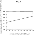
- Fig. 4 is a characteristic of the level shift section 2 depicting changes in the voltage level of the threshold voltage of the input voltage signal S IN with respect to changes in the voltage level of the first power supply voltage V BB .
- the horizontal axis represents changes in the first power supply voltage V BB (V) and the vertical axis represents changes in the threshold voltage.
- V BB the threshold voltage of the input voltage signal S IN
- the threshold voltage of the input voltage signal S IN is 5.43 V.
- the threshold voltage of the input voltage signal S IN changes to 5.24 V.
- the threshold voltage changes linearly with respect to changes in the first power supply voltage V BB .
- the threshold voltage of the input voltage signal S IN may be changed in accordance with changes in the first power supply voltage V BB .
- the electrostatic protection component specifically the third resistor R3, is disposed between the input voltage signal terminal S 1 and the second transistor T2. Therefore, electrostatic breakdown of the second transistor T2 may be prevented or effectively suppressed, and the electrostatic breakdown endurance of the level shifter 1 may be improved.
- an electrostatic breakdown voltage of the second transistor T2 is specified to be high. Therefore, electrostatic breakdown of the second transistor T2 may be prevented or effectively suppressed, and the electrostatic breakdown endurance of the level shifter 1 may be improved.
- the second transistor T2 is a VDMOSFET. Therefore, the electrostatic breakdown voltage of the second transistor T2 may be improved, and the electrostatic breakdown endurance of the level shifter 1 may be improved.
- the buffer section 3 is connected to the output voltage signal terminal S2 of the level shift section 2. Therefore, the waveform of the output voltage signal S OUT that is outputted from the output voltage signal terminal S2 may be shaped using the buffer section 3. Hence, the shaped output voltage signal S OUT1 may ultimately be outputted to the output voltage signal terminal S3 and, similarly, the shaped inverted output voltage signal S OUT2 may ultimately be outputted to the output voltage signal terminal S4.
- the second transistor T2 may be structured by a lateral diffused-type field effect transistor (an LDMOSFET). This transistor has a structure with a higher breakdown voltage.
- an LDMOSFET lateral diffused-type field effect transistor
- the first resistor R1 of the level shift section 2 may be an IGFET of the second conduction type.
- the channel formation region may be utilized as a resistor.
- the circuit configuration of the buffer section 3 of the level shifter 1 may be replaced.
- the buffer section 3 may have a two-stage circuit configuration of the second inverter 31 and the third inverter 32, or may have a circuit configuration with four or more stages.
- the fifth transistor T5, seventh transistor T7 and ninth transistor T9 of the first inverter 30, second inverter 31 and third inverter 32 may be resistors.
- a level shifter that includes: a power supply system current source; a second transistor having a third main electrode that is connected to an input voltage signal terminal, a fourth main electrode that is connected to an output voltage signal terminal, and a second control electrode that is connected to a third power supply voltage having a voltage that is lower than a first power supply voltage and higher than a second power supply voltage; a second resistor; and a third transistor having a fifth main electrode that is connected to the second end of the second resistor, a sixth main electrode that is connected to the second power supply voltage, and a third control electrode that is connected to a first control electrode of a first transistor of the power supply system current source.
Landscapes
- Engineering & Computer Science (AREA)
- Computer Hardware Design (AREA)
- Physics & Mathematics (AREA)
- Computing Systems (AREA)
- General Engineering & Computer Science (AREA)
- Mathematical Physics (AREA)
- Logic Circuits (AREA)
Abstract
Description
- The present invention relates to a level shifter.
- Japanese Patent No.
5,465,548 - When, for example, there is a voltage drop at the in-vehicle battery, then if the threshold voltage is constant, the input voltage signal at the high level may not actually reach the threshold voltage and may be judged to be at a low level. Thus, misoperation may occur. Accordingly, there are calls for a level shifter in which the threshold voltage of an input voltage signal is changed in accordance with voltage changes.
- In consideration of the circumstances described above, the present disclosure provides a level shifter in which a threshold voltage of an input voltage signal may be changed in accordance with a change in a power supply voltage.
- A level shifter according to a first aspect of the present disclosure includes: a power supply system current source including: a first resistor having a first end that is connected to a first power supply voltage, and having a second end, and a first transistor having a first main electrode and a first control electrode that are connected to the second end of the first resistor, and having a second main electrode that is connected to a second power supply voltage having a lower voltage than the first power supply voltage; a second transistor having a third main electrode that is connected to an input voltage signal terminal, a fourth main electrode that is connected to an output voltage signal terminal, and a second control electrode that is connected to a third power supply voltage having a voltage that is lower than the first power supply voltage and higher than the second power supply voltage; a second resistor having a first end that is connected between the fourth main electrode and the output voltage signal terminal, and having a second end; and a third transistor having a fifth main electrode that is connected to the second end of the second resistor, a sixth main electrode that is connected to the second power supply voltage, and a third control electrode that is connected to the first control electrode.
- The level shifter according to the first aspect is provided with the power supply system current source, the second transistor, the second resistor and the third transistor. The power supply system current source includes the first resistor and the first transistor. The one end of the first resistor is connected to the first power supply voltage. The first main electrode and first control electrode of the first transistor is connected to the other end of the first resistor, and the second main electrode of the first transistor is connected to the second power supply voltage. The second power supply voltage is a voltage lower than the first power supply voltage.
- The third main electrode of the second transistor is connected to the input voltage signal terminal, and the fourth main electrode of the second transistor is connected to the output voltage signal terminal. The second control electrode of the second transistor is connected to the third power supply voltage. The third power supply voltage is a voltage lower than the first power supply voltage but higher than the second power supply voltage.
- The one end of the second resistor is connected to between the fourth main electrode of the second transistor and the output voltage signal terminal. The fifth main electrode of the third transistor is connected to the other end of the second resistor, and the sixth main electrode of the third transistor is connected to the second power supply voltage. The third control electrode of the third transistor is connected to the first control electrode of the first transistor.
- Because the third control electrode of the third transistor is connected to the first control electrode of the first transistor, the third transistor constitutes a current mirror circuit with the power supply system current source (the first transistor). At the power supply system current source, a current flowing from the first power supply voltage through the first resistor and first transistor to the second power supply voltage changes in accordance with a change in the voltage level of the first power supply voltage. Thus, the power supply system current source implements current regulation. When an input voltage signal is applied to the input voltage signal terminal, the input voltage signal passes through the second transistor, the second resistor and the third transistor, and is outputted to the second power supply voltage as a current. Thus, the current flowing in the third transistor constituting the current mirror circuit is regulated in accordance with changes in the current flowing in the first transistor of the power supply system current source.
- Therefore, because the current flowing in the second resistor is regulated in accordance with the current regulation of the power supply system current source, the voltage level of a threshold voltage of the input voltage signal may be changed.
- In a level shifter according to a second aspect of the present disclosure, in the level shifter according to the first aspect, an electrostatic protection component is disposed between the input voltage signal terminal and the third main electrode of the second transistor.
- According to the level shifter according to the second aspect, because the electrostatic protection component is disposed between the input voltage signal terminal and the second transistor, electrostatic breakdown of the second transistor may be prevented or effectively suppressed. Therefore, electrostatic breakdown endurance of the level shifter may be improved.
- In a level shifter according to a third aspect of the present disclosure, in the level shifter according to the first aspect or the second aspect, an electrostatic breakdown voltage of the second transistor is higher than respective electrostatic breakdown voltages of the first transistor and the third transistor.
- According to the level shifter according to the third aspect, because the electrostatic breakdown voltage of the second transistor is specified to be higher, electrostatic breakdown of the second transistor may be prevented or effectively suppressed. Therefore, electrostatic breakdown endurance of the level shifter may be improved.
- In a level shifter according to a fourth aspect of the present disclosure, in the level shifter according to any one of the first to third aspects, the second transistor includes a vertical diffused-type transistor.
- According to the level shifter according to the fourth aspect, because the second transistor is a vertical diffused-type transistor, the electrostatic breakdown voltage of the second transistor may be improved. Therefore, electrostatic breakdown endurance of the level shifter may be improved.
- In a level shifter according to a fifth aspect of the present disclosure, the level shifter according to any one of the first to fourth aspects, further includes a buffer section that shapes a waveform of an output voltage signal and that is connected to the output voltage signal terminal.
- According to the level shifter according to the fifth aspect, the waveform of an output voltage signal that is outputted from the output voltage signal terminal may be shaped using the buffer section, and ultimately the shaped output voltage signal may be outputted.
- The level shifter according to the present disclosure provides an excellent effect in that a threshold voltage of an input voltage signal may be changed in accordance with a change in a power supply voltage.
-
-
Fig. 1 is a circuit diagram of a level shifter according to an exemplary embodiment of the present disclosure. -
Fig. 2 is a vertical sectional structural diagram of components structuring a level shift section of the level shifter illustrated inFig. 1 . -
Fig. 3 is a vertical sectional structural diagram, corresponding toFig. 2 , of components structuring a portion of a buffer section of the level shifter illustrated inFig. 1 . -
Fig. 4 is a characteristic of the level shifter illustrated inFig. 1 , depicting changes in a threshold voltage of an input voltage signal SIN with respect to changes in a power supply voltage VBB. - A level shifter according to an exemplary embodiment of the present disclosure is described below using
Fig. 1 to Fig. 4 . In this exemplary embodiment, structural elements that have the same functions or substantially the same functions are assigned the same reference symbols, and duplicative descriptions are omitted. - As illustrated in
Fig. 1 , a level shifter 1 according to the present exemplary embodiment is driven by a first power supply voltage VBB with a high voltage that is supplied from an in-vehicle battery. The level shifter 1 is structured with alevel shift section 2 and abuffer section 3. The level shifter 1 outputs an output voltage signal SOUT1 and an inverted output voltage signal SOUT2, which are level-shifted from the first power supply voltage VBB to a lower voltage in accordance with an input voltage signal SIN at lower voltages than the first power supply voltage VBB. The input voltage signal SIN is applied to an input voltage signal terminal S1 of the level shifter 1. The output voltage signal SOUT1 is outputted to an output voltage signal terminal S3, and the output voltage signal SOUT2 is outputted to an output voltage signal terminal S4. - The first power supply voltage VBB is, for example, between 8 V and 18 V. The input voltage signal SIN is, for example, a rising signal from 0 V (low level) to 6 V (high level) or a falling signal from 6 V to 0 V. The output voltage signal SOUT1 is, for example, a rising signal from 0 V (low level) to 5 V (high level) or a falling signal from 5 V to 0 V. The inverted output voltage signal SOUT2 is an inverted voltage signal of the output voltage signal SOUT1. A second power supply voltage Vss is 0 V.
- The
level shift section 2 of the level shifter 1 includes a power supply systemcurrent source 20, a second transistor T2, a second resistor R2 and a third transistor T3. The power supply systemcurrent source 20 is provided with a first resistor R1 and a first transistor T1. An electrostatic protection component is disposed at thelevel shift section 2. In the present exemplary embodiment, the electrostatic protection component is structured by a third resistor R3. - To describe this in more detail, one end of the first resistor R1 of the power supply system
current source 20 is connected to the first power supply voltage VBB. - The first transistor T1 is structured by an insulated gate field-effect transistor (IGFET) of the n-channel conduction type, which serves as a first conduction type in the present exemplary embodiment. IGFETs include at least metal-oxide-semiconductor (MOS)FETs and metal-insulator-semiconductor (MIS)FETs. A first main electrode (the drain electrode) of the first transistor T1 is connected to the other end of the first resistor R1, and a second main electrode (the source electrode) of the first transistor T1 is connected to the second power supply voltage VSS. A first control electrode (the gate electrode) of the first transistor T1 is connected to both the first resistor R1 and a third control electrode (the gate electrode) of the third transistor T3.
- The second transistor T2 is structured by a high-breakdown-voltage transistor with a higher electrostatic breakdown voltage than an electrostatic breakdown voltage of the first transistor T1. In the present exemplary embodiment, the second transistor T2 is structured by a vertical diffused metal-oxide-semiconductor field effect transistor (VDMOSFET). This second transistor T2 may simply be referred to as a VDMOSFET or a vertical diffused-type transistor). The second transistor T2 is specified to be of the first conduction type.
- A third main electrode (the drain electrode) of the second transistor T2 is connected to the input voltage signal terminal S1, and a fourth main electrode (the source electrode) of the second transistor T2 is connected to an output voltage signal terminal S2 of the
level shift section 2. An output signal voltage SOUT in which the high voltage of the first power supply voltage VBB has been level-shifted to a low voltage is outputted at the output voltage signal terminal S2. A second control electrode (the gate electrode) of the second transistor T2 is connected to a third power supply voltage VCC. This third power supply voltage VCC is a voltage that is lower than the first power supply voltage VBB but higher than the second power supply voltage VSS, specifically being 5 V. The second transistor T2 acts as a clamp transistor that does not output signals above a certain voltage to the output voltage signal terminal S2. - One end of the second resistor R2 is connected to between the fourth main electrode of the second transistor T2 and the output voltage signal terminal S2. The second resistor R2 is used for regulation of a threshold voltage of the input voltage signal SIN.
- The third transistor T3 is structured by an IGFET of the first conduction type, which is constituted with a similar structure to the first transistor T1. A fifth main electrode (the drain electrode) of the third transistor is connected to the other end of the second resistor R2, and a sixth main electrode (the source electrode) of the third transistor T3 is connected to the second power supply voltage VSS. As mentioned above, the third control electrode is connected to the first control electrode of the first transistor T1. Therefore, the third transistor T3 constitutes a current mirror circuit with the first transistor T1.
- The third resistor R3 serves as the electrostatic protection component. One end of the third resistor R3 is connected to the input voltage signal terminal S1, and the other end is connected to the third main electrode of the second transistor T2. Although the electrostatic protection component is structured by the third resistor R3 in the present exemplary embodiment, the electrostatic protection component may be structured in the present exemplary embodiment by using a reverse-connected diode or combining a diode and a resistor.
- In the present exemplary embodiment, the
buffer section 3 of the level shifter 1 includes three stages that are electrically connected in series: afirst inverter 30, asecond inverter 31 and athird inverter 32. - To describe this in more detail, the fourth transistor T4 is structured by an IGFET of the first conduction type. One main electrode of the fourth transistor T4, which is the source electrode, is connected to the second power supply voltage VSS. The other main electrode of the fourth transistor T4, which is the drain electrode, is connected to the other main electrode of the fifth transistor T5, which is the drain electrode thereof, and to gate electrodes of the
second inverter 31. The gate electrode of the fourth transistor T4 is connected to the output voltage signal terminal S2. - The fifth transistor is structured by an IGFET of the p-channel conduction type, which serves as a second conduction type. One main electrode of the fifth transistor T5, which is the source electrode, is connected to the third power supply voltage VCC. The drain electrode of the fifth transistor T5 is connected to the drain electrode of the fourth transistor T4 and to the gate electrodes of the
second inverter 31. The gate electrode of the fifth transistor T5 is connected to the output voltage signal terminal S2. - The
first inverter 30 shapes a waveform of the output voltage signal SOUT that is outputted from the output voltage signal terminal S2. - The
second inverter 31 is arranged as a circuit succeeding thefirst inverter 30, and includes a sixth transistor T6 and a seventh transistor T7. The sixth transistor T6 is constituted with a similar structure to the fourth transistor T4, and the seventh transistor T7 is constituted with a similar constituted to the fifth transistor T5. The gate electrodes of the sixth transistor T6 and the seventh transistor T7 are connected to thefirst inverter 30. The drain electrodes of the sixth transistor T6 and the seventh transistor T7 are connected to thethird inverter 32 and to an output voltage signal terminal S4. The inverted output voltage signal SOUT2 is outputted at the output voltage signal terminal S4. - The
third inverter 32 is arranged as a circuit succeeding thesecond inverter 31, and includes an eighth transistor T8 and a ninth transistor T9. The eighth transistor T8 is constituted with a similar structure to the fourth transistor T4, and the ninth transistor T9 is constituted with a similar structure to the fifth transistor T5. The gate electrodes of the eighth transistor T8 and the ninth transistor T9 are connected to thesecond inverter 31. The drain electrodes of the eighth transistor T8 and the ninth transistor T9 are connected to the output voltage signal terminal S3. The output voltage signal SOUT1 is outputted at the output voltage signal terminal S3. - The level shifter 1 according to the present exemplary embodiment is structured as a semiconductor integrated circuit (a semiconductor device). As illustrated in
Fig. 2 andFig. 3 , the level shifter 1 is formed with asemiconductor substrate 40 serving as a base. In the present exemplary embodiment, an n-type silicon monocrystalline substrate is employed for thesemiconductor substrate 40. - As illustrated in
Fig. 2 , the respective semiconductor components of the level shift section 2-the first resistor R1, second resistor R2 and third resistor R3 and the first transistor T1, second transistor T2 and third transistor T3-are formed on an n-typeepitaxial growth layer 41 that is formed on the principal surface of thesemiconductor substrate 40. The respective semiconductor components are formed within a region of theepitaxial growth layer 41 whose periphery is encircled by acomponent isolation region 42. - The first resistor R1 is formed by a second conduction type (p-type)
semiconductor region 47 disposed in a principal surface portion of a first conduction type (n-type)well region 43 that is formed in theepitaxial growth layer 41. The second resistor R2 and the third resistor R3 are structured with similar vertical cross-section structures to the first resistor R1. - The first transistor T1 is disposed in a principal surface portion of a second conduction
type well region 44 that is formed in theepitaxial growth layer 41. To describe this in more detail, the first transistor T1 is structured with a channel formation region formed by thewell region 44, a pair of first conductiontype semiconductor regions 48 to be used as the first main electrode and the second main electrode, agate isolation layer 50, and agate electrode 51 to serve as the first control electrode. The pair ofsemiconductor regions 48 are formed in principal surface portions of thewell region 44 that are separated from one another with the channel formation region therebetween. Thegate isolation layer 50 is formed on the channel formation region (on the principal surface of the well region 44). Thegate electrode 51 is formed on thegate isolation layer 50. - The third transistor T3 is structured with a similar vertical cross-section structure to the first transistor T1.
- As mentioned above, the second transistor T2 is structured by a VDMOSFET in the present exemplary embodiment. To describe this in more detail, the second transistor T2 is structured with the third main electrode, a channel formation region, the fourth main electrode, another of the
gate isolation layer 50, and another of thegate electrode 51 to serve as the second control electrode. The third main electrode is structured with another of thewell region 43. An impurity density of thewell region 43 is specified to be lower than the impurity densities of thesemiconductor substrate 40 and thesemiconductor region 48. The channel formation region is formed at principal surface portions of second conductiontype base regions 45 that are formed in principal surface portions of thewell region 43 at end portions of thegate electrode 51. Thebase regions 45 connect with second conductiontype semiconductor regions 46 with higher impurity densities than thebase regions 45. The fourth main electrode is formed by another of thesemiconductor region 48 that is formed at a principal surface portion of thebase regions 45. The impurity density of thesemiconductor region 48 is specified to be higher than the impurity density of thesemiconductor substrate 40. Thegate isolation layer 50 is formed on the channel formation region (on the principal surface of the base regions 45), and thegate electrode 51 is formed on thegate isolation layer 50. - Meanwhile, as illustrated in
Fig. 3 , the fourth transistor T4 of thefirst inverter 30 of thebuffer section 3 is formed at the principal surface portion of thewell region 44 within a region whose periphery is encircled by thecomponent isolation region 42. - The fourth transistor T4 is structured with another of the
well region 44 to serve as a channel formation region, another pair of thesemiconductor regions 48 to serve as the one main electrode and the other main electrode, another of thegate isolation layer 50, and another of thegate electrode 51. That is, the fourth transistor T4 is structured with a similar vertical cross-section structure to the first transistor T1 and the third transistor T3. - The fifth transistor T5 is structured with another of the
well region 43 to serve as a channel region, another pair of thesemiconductor regions 47 to serve as the one main electrode and the other main electrode, another of thegate isolation layer 50, and another of thegate electrode 51. - Although not shown in the drawings, the sixth transistor T6 of the
second inverter 31 and the eighth transistor T8 of thethird inverter 32 are structured with similar vertical cross-section structures to the fourth transistor T4, and the seventh transistor T7 of thesecond inverter 31 and the ninth transistor T9 of thethird inverter 32 are structured with similar vertical cross-section structures to the fifth transistor T5. - As illustrated in
Fig. 1 , the level shifter 1 according to the present exemplary embodiment includes thelevel shift section 2. Thelevel shift section 2 is provided with the power supply systemcurrent source 20, the second transistor T2, the second resistor R2 and the third transistor T3. The power supply systemcurrent source 20 includes the first resistor R1 and the first transistor T1. The one end of the first resistor R1 is connected to the first power supply voltage VBB. The first main electrode and first control electrode of the first transistor T1 are connected to the other end of the first resistor R1. The second main electrode of the first transistor VSS is connected to the second power supply voltage Vss. The second power supply voltage VSS is set to a lower voltage than the first power supply voltage VBB. - The third main electrode of the second transistor T2 is connected to the input voltage signal terminal S1, and the fourth main electrode of the second transistor T2 is connected to the output voltage signal electrode S2. The second control electrode of the second transistor T2 is connected to the third power supply voltage VCC. The third power supply voltage VCC is at a voltage lower than the first power supply voltage VBB but higher than the second power supply voltage VSS.
- The one end of the second resistor R2 is connected to between the fourth main electrode of the second transistor T2 and the output voltage signal terminal S2. The fifth main electrode of the third transistor T3 is connected to the other end of the second resistor R2, and the sixth main electrode of the third transistor T3 is connected to the second power supply voltage VSS. The third control electrode of the third transistor T3 is connected to the first control electrode of the first transistor T1.
- Because the third control electrode of the third transistor T3 is connected to the first control electrode of the first transistor T1, the third transistor T3 constitutes a current mirror circuit with the power supply system current source 20 (the first transistor T1). In the power supply system
current source 20, a current flowing from the first power supply voltage VBB through the first resistor R1 and the first transistor T1 to the second power supply voltage VSS changes in accordance with a change in the voltage level of the first power supply voltage VBB. Thus, current regulation is implemented. When the input voltage signal SIN is applied to the input voltage signal terminal S1, the input voltage signal SIN passes through the second transistor T2, the second resistor R2 and the third transistor T3, and is outputted at the second power supply voltage VSS as a current. In accordance with the change in the current flowing in the first transistor T1 of the power supply systemcurrent source 20, the current flowing in the third transistor T3 that constitutes the current mirror circuit is regulated. - Therefore, because the current flowing in the second resistor R2 is regulated in accordance with the current regulation of the power supply system
current source 20, the voltage level of a threshold value of the input voltage signal SIN may be changed. -
Fig. 4 is a characteristic of thelevel shift section 2 depicting changes in the voltage level of the threshold voltage of the input voltage signal SIN with respect to changes in the voltage level of the first power supply voltage VBB. The horizontal axis represents changes in the first power supply voltage VBB (V) and the vertical axis represents changes in the threshold voltage. According to this characteristic, when the first power supply voltage VBB is 16 V, the threshold voltage of the input voltage signal SIN is 5.43 V. If the first power supply voltage VBB falls to 7 V due to a voltage drop, the threshold voltage of the input voltage signal SIN changes to 5.24 V. The threshold voltage changes linearly with respect to changes in the first power supply voltage VBB. - Thus, according to the level shifter 1 according to the present exemplary embodiment, the threshold voltage of the input voltage signal SIN may be changed in accordance with changes in the first power supply voltage VBB.
- Moreover, in the level shifter 1 according to the present exemplary embodiment, as illustrated in
Fig. 1 , the electrostatic protection component, specifically the third resistor R3, is disposed between the input voltage signal terminal S 1 and the second transistor T2. Therefore, electrostatic breakdown of the second transistor T2 may be prevented or effectively suppressed, and the electrostatic breakdown endurance of the level shifter 1 may be improved. - In the level shifter 1 according to the present exemplary embodiment, as illustrated in
Fig. 1 andFig. 2 , an electrostatic breakdown voltage of the second transistor T2 is specified to be high. Therefore, electrostatic breakdown of the second transistor T2 may be prevented or effectively suppressed, and the electrostatic breakdown endurance of the level shifter 1 may be improved. - In the level shifter 1 according to the present exemplary embodiment, as illustrated in
Fig. 1 andFig. 2 , the second transistor T2 is a VDMOSFET. Therefore, the electrostatic breakdown voltage of the second transistor T2 may be improved, and the electrostatic breakdown endurance of the level shifter 1 may be improved. - In the level shifter 1 according to the present exemplary embodiment, as illustrated in
Fig. 1 , thebuffer section 3 is connected to the output voltage signal terminal S2 of thelevel shift section 2. Therefore, the waveform of the output voltage signal SOUT that is outputted from the output voltage signal terminal S2 may be shaped using thebuffer section 3. Hence, the shaped output voltage signal SOUT1 may ultimately be outputted to the output voltage signal terminal S3 and, similarly, the shaped inverted output voltage signal SOUT2 may ultimately be outputted to the output voltage signal terminal S4. - The present disclosure is not limited by the exemplary embodiment described above and may be modified within a scope not departing from the gist; for example, as described below.
- In the
level shift section 2 of the level shifter 1 of the present disclosure, the second transistor T2 may be structured by a lateral diffused-type field effect transistor (an LDMOSFET). This transistor has a structure with a higher breakdown voltage. - In the present disclosure, the first resistor R1 of the
level shift section 2 may be an IGFET of the second conduction type. In an IGFET of the second conduction type, the channel formation region may be utilized as a resistor. - In the present disclosure, the circuit configuration of the
buffer section 3 of the level shifter 1 may be replaced. For example, thebuffer section 3 may have a two-stage circuit configuration of thesecond inverter 31 and thethird inverter 32, or may have a circuit configuration with four or more stages. Moreover, the fifth transistor T5, seventh transistor T7 and ninth transistor T9 of thefirst inverter 30,second inverter 31 andthird inverter 32 may be resistors. - A level shifter that includes: a power supply system current source; a second transistor having a third main electrode that is connected to an input voltage signal terminal, a fourth main electrode that is connected to an output voltage signal terminal, and a second control electrode that is connected to a third power supply voltage having a voltage that is lower than a first power supply voltage and higher than a second power supply voltage; a second resistor; and a third transistor having a fifth main electrode that is connected to the second end of the second resistor, a sixth main electrode that is connected to the second power supply voltage, and a third control electrode that is connected to a first control electrode of a first transistor of the power supply system current source.
Claims (5)
- A level shifter, comprising:a power supply system current source including:a first resistor having a first end that is connected to a first power supply voltage, and having a second end, anda first transistor having a first main electrode and a first control electrode that are connected to the second end of the first resistor, and having a second main electrode that is connected to a second power supply voltage having a lower voltage than the first power supply voltage;a second transistor having a third main electrode that is connected to an input voltage signal terminal, a fourth main electrode that is connected to an output voltage signal terminal, and a second control electrode that is connected to a third power supply voltage having a voltage that is lower than the first power supply voltage and higher than the second power supply voltage;a second resistor having a first end that is connected between the fourth main electrode and the output voltage signal terminal, and having a second end; anda third transistor having a fifth main electrode that is connected to the second end of the second resistor, a sixth main electrode that is connected to the second power supply voltage, and a third control electrode that is connected to the first control electrode.
- The level shifter according to claim 1, wherein an electrostatic protection component is disposed between the input voltage signal terminal and the third main electrode of the second transistor.
- The level shifter according to claim 1 or claim 2, wherein an electrostatic breakdown voltage of the second transistor is higher than respective electrostatic breakdown voltages of the first transistor and the third transistor.
- The level shifter according to any one of claims 1 to 3, wherein the second transistor includes a vertical diffused-type transistor.
- The level shifter according to any one of claims 1 to 4, further comprising a buffer section that shapes a waveform of an output voltage signal and that is connected to the output voltage signal terminal.
Applications Claiming Priority (2)
| Application Number | Priority Date | Filing Date | Title |
|---|---|---|---|
| JP2017011459 | 2017-01-25 | ||
| JP2017194179A JP6493933B2 (en) | 2017-01-25 | 2017-10-04 | Level shifter |
Publications (2)
| Publication Number | Publication Date |
|---|---|
| EP3355473A1 true EP3355473A1 (en) | 2018-08-01 |
| EP3355473B1 EP3355473B1 (en) | 2020-12-23 |
Family
ID=60990621
Family Applications (1)
| Application Number | Title | Priority Date | Filing Date |
|---|---|---|---|
| EP18150031.5A Active EP3355473B1 (en) | 2017-01-25 | 2018-01-02 | Level shifter |
Country Status (3)
| Country | Link |
|---|---|
| US (1) | US10128848B2 (en) |
| EP (1) | EP3355473B1 (en) |
| CN (1) | CN108347243B (en) |
Families Citing this family (4)
| Publication number | Priority date | Publication date | Assignee | Title |
|---|---|---|---|---|
| JP7338821B2 (en) | 2018-11-06 | 2023-09-05 | 株式会社東海理化電機製作所 | signal output circuit |
| US11101789B2 (en) * | 2019-12-19 | 2021-08-24 | Rockwell Automation Technologies, Inc. | Systems and methods for providing bi-directional signal level shifting |
| JP2022108157A (en) * | 2021-01-12 | 2022-07-25 | キオクシア株式会社 | Semiconductor device |
| US20250159879A1 (en) * | 2023-11-14 | 2025-05-15 | Ememory Technology Inc. | Non-volatile memory device for low operation voltage |
Citations (3)
| Publication number | Priority date | Publication date | Assignee | Title |
|---|---|---|---|---|
| WO1996018240A1 (en) * | 1994-12-07 | 1996-06-13 | Philips Electronics N.V. | A protected switch |
| JP5465548B2 (en) | 2010-01-27 | 2014-04-09 | 株式会社東海理化電機製作所 | Level shift circuit |
| US20150358003A1 (en) * | 2013-04-18 | 2015-12-10 | Sharp Kabushiki Kaisha | Level shift circuit |
Family Cites Families (9)
| Publication number | Priority date | Publication date | Assignee | Title |
|---|---|---|---|---|
| JP3635466B2 (en) * | 2002-09-30 | 2005-04-06 | 日本テキサス・インスツルメンツ株式会社 | Level shift circuit |
| JP4075823B2 (en) * | 2004-02-25 | 2008-04-16 | 株式会社デンソー | Comparator circuit device |
| JP4475309B2 (en) * | 2007-09-19 | 2010-06-09 | ヤマハ株式会社 | comparator |
| JP2010109838A (en) * | 2008-10-31 | 2010-05-13 | Nec Electronics Corp | Level shift circuit |
| JP5404235B2 (en) * | 2009-08-03 | 2014-01-29 | 三菱電機株式会社 | Amplitude conversion circuit |
| JP2012134690A (en) * | 2010-12-21 | 2012-07-12 | Mitsumi Electric Co Ltd | Level shift circuit and switching power supply device |
| JP5925625B2 (en) * | 2012-07-19 | 2016-05-25 | 日置電機株式会社 | Overdischarge prevention circuit |
| CN205212814U (en) * | 2015-09-11 | 2016-05-04 | 英特格灵芯片(天津)有限公司 | Level conversion's device |
| CN105827232B (en) * | 2016-03-18 | 2019-01-15 | 苏州芯宽电子科技有限公司 | A kind of restoring circuit improving SSLC level shifting circuit Negative Bias Temperature Instability |
-
2017
- 2017-12-07 CN CN201711284701.2A patent/CN108347243B/en active Active
- 2017-12-27 US US15/854,870 patent/US10128848B2/en active Active
-
2018
- 2018-01-02 EP EP18150031.5A patent/EP3355473B1/en active Active
Patent Citations (3)
| Publication number | Priority date | Publication date | Assignee | Title |
|---|---|---|---|---|
| WO1996018240A1 (en) * | 1994-12-07 | 1996-06-13 | Philips Electronics N.V. | A protected switch |
| JP5465548B2 (en) | 2010-01-27 | 2014-04-09 | 株式会社東海理化電機製作所 | Level shift circuit |
| US20150358003A1 (en) * | 2013-04-18 | 2015-12-10 | Sharp Kabushiki Kaisha | Level shift circuit |
Also Published As
| Publication number | Publication date |
|---|---|
| EP3355473B1 (en) | 2020-12-23 |
| CN108347243A (en) | 2018-07-31 |
| US20180212604A1 (en) | 2018-07-26 |
| US10128848B2 (en) | 2018-11-13 |
| CN108347243B (en) | 2022-04-01 |
Similar Documents
| Publication | Publication Date | Title |
|---|---|---|
| US7692473B2 (en) | Switch circuits with the ability to control latch-up due to a parasitic element | |
| US8975939B2 (en) | Voltage clamp circuit and integrated circuit incorporating same | |
| EP3355473B1 (en) | Level shifter | |
| JP2011029912A (en) | Reference voltage circuit and electronic device | |
| US8836380B2 (en) | Bootstrap circuit | |
| JP6493933B2 (en) | Level shifter | |
| US20180083618A1 (en) | Switch apparatus | |
| US8836027B2 (en) | Switch circuit using LDMOS element | |
| JP7597785B2 (en) | Clamp Circuit | |
| US10312913B2 (en) | Level shifter | |
| JP2017055214A (en) | Level shift circuit | |
| CN113035860B (en) | Electrostatic protection circuit and semiconductor device | |
| US11750098B2 (en) | Voltage conversion circuit having self-adaptive mechanism | |
| KR0142001B1 (en) | Semiconductor integrated circuit device | |
| US9166047B2 (en) | Switch circuit using LDMOS device | |
| US20020175373A1 (en) | Semiconductor device | |
| US20250373247A1 (en) | Analog switch | |
| US9843322B2 (en) | Integrated high-side driver for P-N bimodal power device | |
| JPS6232722A (en) | Push-pull output circuit | |
| US20250192540A1 (en) | Protection circuit and semiconductor device including the protection circuit | |
| US20250309900A1 (en) | Logic gate circuit | |
| WO1987003759A1 (en) | Electronic interface circuit | |
| JP4658360B2 (en) | Output buffer | |
| JP2026002123A (en) | Voltage Generation Circuit | |
| TW202011136A (en) | Constant current circuit |
Legal Events
| Date | Code | Title | Description |
|---|---|---|---|
| PUAI | Public reference made under article 153(3) epc to a published international application that has entered the european phase |
Free format text: ORIGINAL CODE: 0009012 |
|
| STAA | Information on the status of an ep patent application or granted ep patent |
Free format text: STATUS: THE APPLICATION HAS BEEN PUBLISHED |
|
| AK | Designated contracting states |
Kind code of ref document: A1 Designated state(s): AL AT BE BG CH CY CZ DE DK EE ES FI FR GB GR HR HU IE IS IT LI LT LU LV MC MK MT NL NO PL PT RO RS SE SI SK SM TR |
|
| AX | Request for extension of the european patent |
Extension state: BA ME |
|
| STAA | Information on the status of an ep patent application or granted ep patent |
Free format text: STATUS: REQUEST FOR EXAMINATION WAS MADE |
|
| 17P | Request for examination filed |
Effective date: 20180905 |
|
| RBV | Designated contracting states (corrected) |
Designated state(s): AL AT BE BG CH CY CZ DE DK EE ES FI FR GB GR HR HU IE IS IT LI LT LU LV MC MK MT NL NO PL PT RO RS SE SI SK SM TR |
|
| GRAP | Despatch of communication of intention to grant a patent |
Free format text: ORIGINAL CODE: EPIDOSNIGR1 |
|
| STAA | Information on the status of an ep patent application or granted ep patent |
Free format text: STATUS: GRANT OF PATENT IS INTENDED |
|
| INTG | Intention to grant announced |
Effective date: 20200812 |
|
| RIN1 | Information on inventor provided before grant (corrected) |
Inventor name: MATSUBARA, JUNICHI |
|
| GRAS | Grant fee paid |
Free format text: ORIGINAL CODE: EPIDOSNIGR3 |
|
| GRAA | (expected) grant |
Free format text: ORIGINAL CODE: 0009210 |
|
| STAA | Information on the status of an ep patent application or granted ep patent |
Free format text: STATUS: THE PATENT HAS BEEN GRANTED |
|
| AK | Designated contracting states |
Kind code of ref document: B1 Designated state(s): AL AT BE BG CH CY CZ DE DK EE ES FI FR GB GR HR HU IE IS IT LI LT LU LV MC MK MT NL NO PL PT RO RS SE SI SK SM TR |
|
| REG | Reference to a national code |
Ref country code: GB Ref legal event code: FG4D |
|
| REG | Reference to a national code |
Ref country code: DE Ref legal event code: R096 Ref document number: 602018010946 Country of ref document: DE |
|
| REG | Reference to a national code |
Ref country code: AT Ref legal event code: REF Ref document number: 1348706 Country of ref document: AT Kind code of ref document: T Effective date: 20210115 |
|
| REG | Reference to a national code |
Ref country code: IE Ref legal event code: FG4D |
|
| PG25 | Lapsed in a contracting state [announced via postgrant information from national office to epo] |
Ref country code: RS Free format text: LAPSE BECAUSE OF FAILURE TO SUBMIT A TRANSLATION OF THE DESCRIPTION OR TO PAY THE FEE WITHIN THE PRESCRIBED TIME-LIMIT Effective date: 20201223 Ref country code: FI Free format text: LAPSE BECAUSE OF FAILURE TO SUBMIT A TRANSLATION OF THE DESCRIPTION OR TO PAY THE FEE WITHIN THE PRESCRIBED TIME-LIMIT Effective date: 20201223 Ref country code: NO Free format text: LAPSE BECAUSE OF FAILURE TO SUBMIT A TRANSLATION OF THE DESCRIPTION OR TO PAY THE FEE WITHIN THE PRESCRIBED TIME-LIMIT Effective date: 20210323 Ref country code: GR Free format text: LAPSE BECAUSE OF FAILURE TO SUBMIT A TRANSLATION OF THE DESCRIPTION OR TO PAY THE FEE WITHIN THE PRESCRIBED TIME-LIMIT Effective date: 20210324 |
|
| REG | Reference to a national code |
Ref country code: AT Ref legal event code: MK05 Ref document number: 1348706 Country of ref document: AT Kind code of ref document: T Effective date: 20201223 |
|
| REG | Reference to a national code |
Ref country code: NL Ref legal event code: MP Effective date: 20201223 |
|
| PG25 | Lapsed in a contracting state [announced via postgrant information from national office to epo] |
Ref country code: BG Free format text: LAPSE BECAUSE OF FAILURE TO SUBMIT A TRANSLATION OF THE DESCRIPTION OR TO PAY THE FEE WITHIN THE PRESCRIBED TIME-LIMIT Effective date: 20210323 Ref country code: LV Free format text: LAPSE BECAUSE OF FAILURE TO SUBMIT A TRANSLATION OF THE DESCRIPTION OR TO PAY THE FEE WITHIN THE PRESCRIBED TIME-LIMIT Effective date: 20201223 Ref country code: SE Free format text: LAPSE BECAUSE OF FAILURE TO SUBMIT A TRANSLATION OF THE DESCRIPTION OR TO PAY THE FEE WITHIN THE PRESCRIBED TIME-LIMIT Effective date: 20201223 |
|
| PG25 | Lapsed in a contracting state [announced via postgrant information from national office to epo] |
Ref country code: NL Free format text: LAPSE BECAUSE OF FAILURE TO SUBMIT A TRANSLATION OF THE DESCRIPTION OR TO PAY THE FEE WITHIN THE PRESCRIBED TIME-LIMIT Effective date: 20201223 Ref country code: HR Free format text: LAPSE BECAUSE OF FAILURE TO SUBMIT A TRANSLATION OF THE DESCRIPTION OR TO PAY THE FEE WITHIN THE PRESCRIBED TIME-LIMIT Effective date: 20201223 |
|
| REG | Reference to a national code |
Ref country code: LT Ref legal event code: MG9D |
|
| PG25 | Lapsed in a contracting state [announced via postgrant information from national office to epo] |
Ref country code: PT Free format text: LAPSE BECAUSE OF FAILURE TO SUBMIT A TRANSLATION OF THE DESCRIPTION OR TO PAY THE FEE WITHIN THE PRESCRIBED TIME-LIMIT Effective date: 20210423 Ref country code: SK Free format text: LAPSE BECAUSE OF FAILURE TO SUBMIT A TRANSLATION OF THE DESCRIPTION OR TO PAY THE FEE WITHIN THE PRESCRIBED TIME-LIMIT Effective date: 20201223 Ref country code: RO Free format text: LAPSE BECAUSE OF FAILURE TO SUBMIT A TRANSLATION OF THE DESCRIPTION OR TO PAY THE FEE WITHIN THE PRESCRIBED TIME-LIMIT Effective date: 20201223 Ref country code: SM Free format text: LAPSE BECAUSE OF FAILURE TO SUBMIT A TRANSLATION OF THE DESCRIPTION OR TO PAY THE FEE WITHIN THE PRESCRIBED TIME-LIMIT Effective date: 20201223 Ref country code: LT Free format text: LAPSE BECAUSE OF FAILURE TO SUBMIT A TRANSLATION OF THE DESCRIPTION OR TO PAY THE FEE WITHIN THE PRESCRIBED TIME-LIMIT Effective date: 20201223 Ref country code: EE Free format text: LAPSE BECAUSE OF FAILURE TO SUBMIT A TRANSLATION OF THE DESCRIPTION OR TO PAY THE FEE WITHIN THE PRESCRIBED TIME-LIMIT Effective date: 20201223 Ref country code: CZ Free format text: LAPSE BECAUSE OF FAILURE TO SUBMIT A TRANSLATION OF THE DESCRIPTION OR TO PAY THE FEE WITHIN THE PRESCRIBED TIME-LIMIT Effective date: 20201223 |
|
| PG25 | Lapsed in a contracting state [announced via postgrant information from national office to epo] |
Ref country code: AT Free format text: LAPSE BECAUSE OF FAILURE TO SUBMIT A TRANSLATION OF THE DESCRIPTION OR TO PAY THE FEE WITHIN THE PRESCRIBED TIME-LIMIT Effective date: 20201223 Ref country code: PL Free format text: LAPSE BECAUSE OF FAILURE TO SUBMIT A TRANSLATION OF THE DESCRIPTION OR TO PAY THE FEE WITHIN THE PRESCRIBED TIME-LIMIT Effective date: 20201223 |
|
| REG | Reference to a national code |
Ref country code: CH Ref legal event code: PL |
|
| REG | Reference to a national code |
Ref country code: DE Ref legal event code: R097 Ref document number: 602018010946 Country of ref document: DE |
|
| PG25 | Lapsed in a contracting state [announced via postgrant information from national office to epo] |
Ref country code: IS Free format text: LAPSE BECAUSE OF FAILURE TO SUBMIT A TRANSLATION OF THE DESCRIPTION OR TO PAY THE FEE WITHIN THE PRESCRIBED TIME-LIMIT Effective date: 20210423 Ref country code: MC Free format text: LAPSE BECAUSE OF FAILURE TO SUBMIT A TRANSLATION OF THE DESCRIPTION OR TO PAY THE FEE WITHIN THE PRESCRIBED TIME-LIMIT Effective date: 20201223 Ref country code: LU Free format text: LAPSE BECAUSE OF NON-PAYMENT OF DUE FEES Effective date: 20210102 |
|
| REG | Reference to a national code |
Ref country code: BE Ref legal event code: MM Effective date: 20210131 |
|
| PG25 | Lapsed in a contracting state [announced via postgrant information from national office to epo] |
Ref country code: IT Free format text: LAPSE BECAUSE OF FAILURE TO SUBMIT A TRANSLATION OF THE DESCRIPTION OR TO PAY THE FEE WITHIN THE PRESCRIBED TIME-LIMIT Effective date: 20201223 Ref country code: AL Free format text: LAPSE BECAUSE OF FAILURE TO SUBMIT A TRANSLATION OF THE DESCRIPTION OR TO PAY THE FEE WITHIN THE PRESCRIBED TIME-LIMIT Effective date: 20201223 |
|
| PLBE | No opposition filed within time limit |
Free format text: ORIGINAL CODE: 0009261 |
|
| STAA | Information on the status of an ep patent application or granted ep patent |
Free format text: STATUS: NO OPPOSITION FILED WITHIN TIME LIMIT |
|
| PG25 | Lapsed in a contracting state [announced via postgrant information from national office to epo] |
Ref country code: LI Free format text: LAPSE BECAUSE OF NON-PAYMENT OF DUE FEES Effective date: 20210131 Ref country code: CH Free format text: LAPSE BECAUSE OF NON-PAYMENT OF DUE FEES Effective date: 20210131 Ref country code: DK Free format text: LAPSE BECAUSE OF FAILURE TO SUBMIT A TRANSLATION OF THE DESCRIPTION OR TO PAY THE FEE WITHIN THE PRESCRIBED TIME-LIMIT Effective date: 20201223 |
|
| 26N | No opposition filed |
Effective date: 20210924 |
|
| PG25 | Lapsed in a contracting state [announced via postgrant information from national office to epo] |
Ref country code: ES Free format text: LAPSE BECAUSE OF FAILURE TO SUBMIT A TRANSLATION OF THE DESCRIPTION OR TO PAY THE FEE WITHIN THE PRESCRIBED TIME-LIMIT Effective date: 20201223 Ref country code: FR Free format text: LAPSE BECAUSE OF NON-PAYMENT OF DUE FEES Effective date: 20210223 Ref country code: IE Free format text: LAPSE BECAUSE OF NON-PAYMENT OF DUE FEES Effective date: 20210102 |
|
| PG25 | Lapsed in a contracting state [announced via postgrant information from national office to epo] |
Ref country code: SI Free format text: LAPSE BECAUSE OF FAILURE TO SUBMIT A TRANSLATION OF THE DESCRIPTION OR TO PAY THE FEE WITHIN THE PRESCRIBED TIME-LIMIT Effective date: 20201223 |
|
| PG25 | Lapsed in a contracting state [announced via postgrant information from national office to epo] |
Ref country code: IS Free format text: LAPSE BECAUSE OF FAILURE TO SUBMIT A TRANSLATION OF THE DESCRIPTION OR TO PAY THE FEE WITHIN THE PRESCRIBED TIME-LIMIT Effective date: 20210423 |
|
| PG25 | Lapsed in a contracting state [announced via postgrant information from national office to epo] |
Ref country code: BE Free format text: LAPSE BECAUSE OF NON-PAYMENT OF DUE FEES Effective date: 20210131 |
|
| GBPC | Gb: european patent ceased through non-payment of renewal fee |
Effective date: 20220102 |
|
| PG25 | Lapsed in a contracting state [announced via postgrant information from national office to epo] |
Ref country code: GB Free format text: LAPSE BECAUSE OF NON-PAYMENT OF DUE FEES Effective date: 20220102 |
|
| PG25 | Lapsed in a contracting state [announced via postgrant information from national office to epo] |
Ref country code: CY Free format text: LAPSE BECAUSE OF FAILURE TO SUBMIT A TRANSLATION OF THE DESCRIPTION OR TO PAY THE FEE WITHIN THE PRESCRIBED TIME-LIMIT Effective date: 20201223 |
|
| PG25 | Lapsed in a contracting state [announced via postgrant information from national office to epo] |
Ref country code: HU Free format text: LAPSE BECAUSE OF FAILURE TO SUBMIT A TRANSLATION OF THE DESCRIPTION OR TO PAY THE FEE WITHIN THE PRESCRIBED TIME-LIMIT; INVALID AB INITIO Effective date: 20180102 |
|
| PG25 | Lapsed in a contracting state [announced via postgrant information from national office to epo] |
Ref country code: MK Free format text: LAPSE BECAUSE OF FAILURE TO SUBMIT A TRANSLATION OF THE DESCRIPTION OR TO PAY THE FEE WITHIN THE PRESCRIBED TIME-LIMIT Effective date: 20201223 |
|
| PG25 | Lapsed in a contracting state [announced via postgrant information from national office to epo] |
Ref country code: TR Free format text: LAPSE BECAUSE OF FAILURE TO SUBMIT A TRANSLATION OF THE DESCRIPTION OR TO PAY THE FEE WITHIN THE PRESCRIBED TIME-LIMIT Effective date: 20201223 |
|
| PG25 | Lapsed in a contracting state [announced via postgrant information from national office to epo] |
Ref country code: MT Free format text: LAPSE BECAUSE OF FAILURE TO SUBMIT A TRANSLATION OF THE DESCRIPTION OR TO PAY THE FEE WITHIN THE PRESCRIBED TIME-LIMIT Effective date: 20201223 |
|
| PGFP | Annual fee paid to national office [announced via postgrant information from national office to epo] |
Ref country code: DE Payment date: 20251203 Year of fee payment: 9 |