EP3355471B1 - Class ab amplifier having cascode stage with filter for improving linearity - Google Patents
Class ab amplifier having cascode stage with filter for improving linearity Download PDFInfo
- Publication number
- EP3355471B1 EP3355471B1 EP18150897.9A EP18150897A EP3355471B1 EP 3355471 B1 EP3355471 B1 EP 3355471B1 EP 18150897 A EP18150897 A EP 18150897A EP 3355471 B1 EP3355471 B1 EP 3355471B1
- Authority
- EP
- European Patent Office
- Prior art keywords
- von
- stage
- class
- amplifier
- input signal
- Prior art date
- Legal status (The legal status is an assumption and is not a legal conclusion. Google has not performed a legal analysis and makes no representation as to the accuracy of the status listed.)
- Active
Links
Images



Classifications
-
- H—ELECTRICITY
- H03—ELECTRONIC CIRCUITRY
- H03F—AMPLIFIERS
- H03F1/00—Details of amplifiers with only discharge tubes, only semiconductor devices or only unspecified devices as amplifying elements
- H03F1/32—Modifications of amplifiers to reduce non-linear distortion
- H03F1/3211—Modifications of amplifiers to reduce non-linear distortion in differential amplifiers
-
- H—ELECTRICITY
- H03—ELECTRONIC CIRCUITRY
- H03F—AMPLIFIERS
- H03F1/00—Details of amplifiers with only discharge tubes, only semiconductor devices or only unspecified devices as amplifying elements
- H03F1/08—Modifications of amplifiers to reduce detrimental influences of internal impedances of amplifying elements
- H03F1/22—Modifications of amplifiers to reduce detrimental influences of internal impedances of amplifying elements by use of cascode coupling, i.e. earthed cathode or emitter stage followed by earthed grid or base stage respectively
- H03F1/223—Modifications of amplifiers to reduce detrimental influences of internal impedances of amplifying elements by use of cascode coupling, i.e. earthed cathode or emitter stage followed by earthed grid or base stage respectively with MOSFET's
-
- H—ELECTRICITY
- H03—ELECTRONIC CIRCUITRY
- H03F—AMPLIFIERS
- H03F3/00—Amplifiers with only discharge tubes or only semiconductor devices as amplifying elements
- H03F3/20—Power amplifiers, e.g. Class B amplifiers, Class C amplifiers
- H03F3/21—Power amplifiers, e.g. Class B amplifiers, Class C amplifiers with semiconductor devices only
-
- H—ELECTRICITY
- H03—ELECTRONIC CIRCUITRY
- H03F—AMPLIFIERS
- H03F3/00—Amplifiers with only discharge tubes or only semiconductor devices as amplifying elements
- H03F3/30—Single-ended push-pull [SEPP] amplifiers; Phase-splitters therefor
- H03F3/3001—Single-ended push-pull [SEPP] amplifiers; Phase-splitters therefor with field-effect transistors
- H03F3/3022—CMOS common source output SEPP amplifiers
- H03F3/3023—CMOS common source output SEPP amplifiers with asymmetrical driving of the end stage
-
- H—ELECTRICITY
- H03—ELECTRONIC CIRCUITRY
- H03F—AMPLIFIERS
- H03F3/00—Amplifiers with only discharge tubes or only semiconductor devices as amplifying elements
- H03F3/45—Differential amplifiers
- H03F3/45071—Differential amplifiers with semiconductor devices only
- H03F3/45076—Differential amplifiers with semiconductor devices only characterised by the way of implementation of the active amplifying circuit in the differential amplifier
- H03F3/45179—Differential amplifiers with semiconductor devices only characterised by the way of implementation of the active amplifying circuit in the differential amplifier using MOSFET transistors as the active amplifying circuit
- H03F3/45183—Long tailed pairs
- H03F3/45188—Non-folded cascode stages
-
- H—ELECTRICITY
- H03—ELECTRONIC CIRCUITRY
- H03F—AMPLIFIERS
- H03F3/00—Amplifiers with only discharge tubes or only semiconductor devices as amplifying elements
- H03F3/45—Differential amplifiers
- H03F3/45071—Differential amplifiers with semiconductor devices only
- H03F3/45076—Differential amplifiers with semiconductor devices only characterised by the way of implementation of the active amplifying circuit in the differential amplifier
- H03F3/45179—Differential amplifiers with semiconductor devices only characterised by the way of implementation of the active amplifying circuit in the differential amplifier using MOSFET transistors as the active amplifying circuit
- H03F3/45183—Long tailed pairs
- H03F3/45192—Folded cascode stages
-
- H—ELECTRICITY
- H03—ELECTRONIC CIRCUITRY
- H03F—AMPLIFIERS
- H03F3/00—Amplifiers with only discharge tubes or only semiconductor devices as amplifying elements
- H03F3/45—Differential amplifiers
- H03F3/45071—Differential amplifiers with semiconductor devices only
- H03F3/45076—Differential amplifiers with semiconductor devices only characterised by the way of implementation of the active amplifying circuit in the differential amplifier
- H03F3/45179—Differential amplifiers with semiconductor devices only characterised by the way of implementation of the active amplifying circuit in the differential amplifier using MOSFET transistors as the active amplifying circuit
- H03F3/4521—Complementary long tailed pairs having parallel inputs and being supplied in parallel
-
- H—ELECTRICITY
- H03—ELECTRONIC CIRCUITRY
- H03F—AMPLIFIERS
- H03F3/00—Amplifiers with only discharge tubes or only semiconductor devices as amplifying elements
- H03F3/45—Differential amplifiers
- H03F3/45071—Differential amplifiers with semiconductor devices only
- H03F3/45076—Differential amplifiers with semiconductor devices only characterised by the way of implementation of the active amplifying circuit in the differential amplifier
- H03F3/45179—Differential amplifiers with semiconductor devices only characterised by the way of implementation of the active amplifying circuit in the differential amplifier using MOSFET transistors as the active amplifying circuit
- H03F3/4521—Complementary long tailed pairs having parallel inputs and being supplied in parallel
- H03F3/45219—Folded cascode stages
-
- H—ELECTRICITY
- H03—ELECTRONIC CIRCUITRY
- H03F—AMPLIFIERS
- H03F2200/00—Indexing scheme relating to amplifiers
- H03F2200/165—A filter circuit coupled to the input of an amplifier
-
- H—ELECTRICITY
- H03—ELECTRONIC CIRCUITRY
- H03F—AMPLIFIERS
- H03F2200/00—Indexing scheme relating to amplifiers
- H03F2200/168—Two amplifying stages are coupled by means of a filter circuit
-
- H—ELECTRICITY
- H03—ELECTRONIC CIRCUITRY
- H03F—AMPLIFIERS
- H03F2203/00—Indexing scheme relating to amplifiers with only discharge tubes or only semiconductor devices as amplifying elements covered by H03F3/00
- H03F2203/45—Indexing scheme relating to differential amplifiers
- H03F2203/45028—Indexing scheme relating to differential amplifiers the differential amplifier amplifying transistors are folded cascode coupled transistors
-
- H—ELECTRICITY
- H03—ELECTRONIC CIRCUITRY
- H03F—AMPLIFIERS
- H03F2203/00—Indexing scheme relating to amplifiers with only discharge tubes or only semiconductor devices as amplifying elements covered by H03F3/00
- H03F2203/45—Indexing scheme relating to differential amplifiers
- H03F2203/45134—Indexing scheme relating to differential amplifiers the whole differential amplifier together with other coupled stages being fully differential realised
-
- H—ELECTRICITY
- H03—ELECTRONIC CIRCUITRY
- H03F—AMPLIFIERS
- H03F2203/00—Indexing scheme relating to amplifiers with only discharge tubes or only semiconductor devices as amplifying elements covered by H03F3/00
- H03F2203/45—Indexing scheme relating to differential amplifiers
- H03F2203/45296—Indexing scheme relating to differential amplifiers the AAC comprising one or more discrete capacitive elements, e.g. a transistor coupled as capacitor
-
- H—ELECTRICITY
- H03—ELECTRONIC CIRCUITRY
- H03F—AMPLIFIERS
- H03F2203/00—Indexing scheme relating to amplifiers with only discharge tubes or only semiconductor devices as amplifying elements covered by H03F3/00
- H03F2203/45—Indexing scheme relating to differential amplifiers
- H03F2203/45298—Indexing scheme relating to differential amplifiers the AAC comprising one or more combinations of discrete capacitor and resistor elements, e.g. active elements using a transistor as a capacitor or as a resistor
-
- H—ELECTRICITY
- H03—ELECTRONIC CIRCUITRY
- H03F—AMPLIFIERS
- H03F2203/00—Indexing scheme relating to amplifiers with only discharge tubes or only semiconductor devices as amplifying elements covered by H03F3/00
- H03F2203/45—Indexing scheme relating to differential amplifiers
- H03F2203/45302—Indexing scheme relating to differential amplifiers the common gate stage of a cascode dif amp being controlled
Definitions
- a static class AB amplifier is widely used in filter design because of its good efficiency to drive load.
- the static class AB amplifier generally has a stage positioned before an output stage to set appropriate DC levels to the output stage, and because a transconductance and an output resistance of this stage vary with a signal swing, the variations of the transconductance and the output resistance will generate distortion.
- the distortion cannot be suppressed by loop gain at high frequency, meaning that a linearity of the class AB amplifier is dominated by the distortion/nonlinearity of this stage.
- IM3 third-order intermodulation distortion
- FCC Federal Communications Commission
- US 2015/381116 A1 describes a power amplifier including a gain stage, an output stage and a first capacitor.
- US 2013/200953 A1 describes an operational amplifier circuit which includes a first stage amplifier circuit, a second stage amplifier circuit and a first feed-forward circuit.
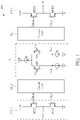
- FIG. 1 is a diagram illustrating a class AB amplifier 100 according to one example.
- the class AB amplifier 100 comprises an input stage 110, two cascode stages 120_1 and 120_2, and two output stages 130_1 and 130_2.
- the class AB amplifier 100 is a static class AB amplifier, meaning that the class AB amplifier 100 always operates as class AB.
- the input stage 110 comprises two P-type metal oxide semiconductor (PMOS) MP1 and MP2 and three current sources I1, I2 and I3, where the current source I1 is coupled between a supply voltage VDD and source electrodes of the PMOSs MP1 and MP2, and the current sources I2 and I3 are coupled between a ground voltage and drain electrodes of the PMOSs MP1 and MP2, respectively.
- the input stage 110 is arranged to receive differential input signals Vip and Vin to generate a differential amplified input signals Von and Vop.
- the cascode stage 120_1 is arranged to generate driving signals Von_p and Von_n according to the amplified input signal Von
- the cascode stage 120_2 is arranged to generate driving signals Vop_p and Vop_n according to the amplified input signal Vop.
- the output stage 130_1 comprises a PMOS MOP1 and an NMOS MON1, and is arranged to generate an output signal Vout_N according to the driving signals Von_p and Von_n; and the output stage 130_2 comprises a PMOS MOP2 and an NMOS MON2, and is arranged to generate an output signal Vout_P according to the driving signals Vop_p and Vop_n, wherein the output signals Vout_N and Vout_P are a differential pair.
- the cascode stage 120_1 is arranged to generate the driving signals Von_p and Von_n with appropriate DC levels to make the output stage 130_1 operate as a class AB output stage, and the cascode stage 120_1 further comprises a filter such as a high-pass filter to make the driving signals Von_p and Von_n have AC components of the amplified input signal Von.
- the cascode stage 120_2 is arranged to generate the driving signals Vop_p and Vop_n with appropriate DC levels to make the output stage 130_2 operate as a class AB output stage, and the cascode stage 120_2 further comprises a filter such as a high-pass filter to make the driving signals Vop_p and Vop_n have AC components of the amplified input signal Von.
- a filter such as a high-pass filter to make the driving signals Vop_p and Vop_n have AC components of the amplified input signal Von.
- FIG. 2 is a diagram illustrating the cascode stage 120_1 according to one example.
- the cascode stage 120_1 comprises a high-pass filter 222, a PMOS MFP1, an NMOS MFN1, and two current sources I4 and I5, wherein the high-pass filter 222 comprises a capacitor C1 and a resistor R1.
- the cascode stage 120_1 shown in FIG. 2 comprises a high-pass filter 222, a PMOS MFP1, an NMOS MFN1, and two current sources I4 and I5, wherein the high-pass filter 222 comprises a capacitor C1 and a resistor R1.
- a gate electrode of the PMOS MFP1 is biased by a bias voltage Vbp divided by the resistor R1 and the capacitor C1
- a gate electrode of the NMOS MFN1 is biased by a bias voltage Vbn
- the PMOS MFP1 and the NMOS MFN1 are used to provide an appropriate DC offset to the driving signal Von_p to make the PMOS MOP1 of the output stage 130_1 operate in a saturation region; and the amplified input signal Von serves as the driving signal Von_n.
- the cascode stage 120_1 can be considered to provide additional gain to the output stage 130_1, and the voltage swing of the amplified input signals Von can be reduced, and the distortion/nonlinearity of the class AB amplifier 100 is improved due to the lower voltage swing of the amplified input signals Von.
- a corner of the high-pass filter 222 can be chosen at a higher frequency such as 40MHz, and the resistor R1 and the capacitor C1 can be designed to be smaller to save the manufacturing cost.
- the circuits shown in FIG. 2 are for illustrative purposes only, and they are not limitations of the present invention.
- the high-pass filter 222 may have other circuit designs or the high-pass filter 222 may be replaced by a band-pass filter.
- one or more transistors can be positioned between the current source I4 and the source electrodes of the PMOS MFP1 (drain electrode of the NMOS MFN1), one or more transistors can be positioned between the current source I5 and the drain electrode of the PMOS MFP1 (source electrode of the NMOS MFN1), one or more transistors can be positioned between the PMOS MOP1 and the supply voltage VDD, and/or one or more transistors are positioned between the NMOS MON1 and the ground voltage.
- FIG. 3 is a diagram illustrating the cascode stage 120_1 according to another example of the present invention.
- the cascode stage 120_1 comprises a high-pass filter 322, a PMOS MFP2, an NMOS MFN2, and two current sources I6 and I7, wherein the high-pass filter 322 comprises a capacitor C2 and a resistor R2.
- the high-pass filter 322 comprises a capacitor C2 and a resistor R2.
- a gate electrode of the NMOS MFN2 is biased by a bias voltage Vbn divided by the resistor R2 and the capacitor C2
- a gate electrode of the PMOS MFP2 is biased by a bias voltage Vbp
- the amplified input signal Von serves as the driving signal Von_p.
- the cascode stage 120_1 can be considered to provide additional gain to the output stage 130_1, and the voltage swing of the amplified input signals Von can be reduced, and the distortion/nonlinearity of the class AB amplifier 100 is improved due to the lower voltage swing of the amplified input signals Von.
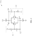
- FIG. 4 is a diagram illustrating the cascode stage 120_1 according to an embodiment of the present invention.
- the cascode stage 120_1 comprises two high-pass filters 422 and 424, a PMOS MFP3, an NMOS MFN3, and two current sources I8 and I9, wherein the high-pass filter 422 comprises a capacitor C3 and a resistor R3, and the high-pass filter 424 comprises a capacitor C4 and a resistor R4.
- a gate electrode of the PMOS MFP3 is biased by a bias voltage Vbp divided by the resistor R3 and the capacitor C3
- a gate electrode of the NMOS MFN3 is biased by a bias voltage Vbn divided by the resistor R4 and the capacitor C4.
- the embodiment shown in FIG. 4 is a combination of the examples shown in FIG. 2 and FIG. 3 , and similarly, the voltage swing of the amplified input signals Von shown in FIG. 4 can be reduced, and the distortion/nonlinearity of the class AB amplifier 100 is improved due to the lower voltage swing of the amplified input signals Von.
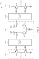
- FIG. 5 is a diagram illustrating a class AB amplifier 500 according to another embodiment of the present invention.
- the class AB amplifier 500 comprises an input stage 510, cascode stages 520_1 and 520_2, and output stages 530_1 and 530_2.
- the class AB amplifier 500 is a static class AB amplifier, that is the class AB amplifier 500 is always operates as class AB.
- the input stage 510 comprises two NMOS MN1 and MN2, and three current sources I1', I2' and I3', where the current source I1' is coupled between the ground voltage and source electrodes of the NMOSs MN1 and MN2, and the current sources I2' and I3' are coupled between the supply voltage VDD and drain electrodes of the NMOSs MN1 and MN2, respectively.
- the input stage 510 is arranged to receive differential input signals Vip and Vin to generate a differential amplified input signals Von and Vop.
- the cascode stage 520 1 is arranged to generate driving signals Von_p and Von_n according to the amplified input signal Von, and the cascode stage 5120_2 is arranged to generate driving signals Vop_p and Vop_n according to the amplified input signal Vop.
- the output stage 530_1 comprises a PMOS MOP1 and an NMOS MON1, and is arranged to generate an output signal Vout N according to the driving signals Von_p and Von n; and the output stage 530_2 comprises a PMOS MOP2 and an NMOS MON2, and is arranged to generate an output signal Vout_P according to the driving signals Vop_p and Vop_n, wherein the output signals Vout_N and Vout_P are a differential pair.
- the class AB amplifier 500 is similar to the class AB amplifier 100 shown in FIG. 1 except for the input stage 510, and the operations and circuit designs of the cascode stages 520_1 and 520_2 are implemented according to the embodiment shown in FIG. 4 . Further descriptions are therefore omitted here.
- FIG. 6 is a diagram illustrating a class AB amplifier 600 according to another embodiment of the present invention.
- the class AB amplifier 600 comprises an input stage 610, cascode stages 620_1 and 620_2, and output stages 630_1 and 630_2.
- the class AB amplifier 600 is a static class AB amplifier, that is the class AB amplifier 600 is always operates as class AB.
- the input stage 610 comprises two PMOSs MP1' and MP2', two NMOSs MN1' and MN2', and two current sources I1" and 12", where the current source I1" is coupled between the supply voltage VDD and source electrodes of the PMOSs MP1 and MP2, and the current source I2" is coupled between the ground voltage and source electrodes of the NMOSs MN1 and MN2.
- the input stage 610 is arranged to receive differential input signals Vip and Vin to generate a differential amplified input signals.
- the cascode stage 620_1 is arranged to generate driving signals Von_p and Von_n according to the amplified input signal
- the cascode stage 620_2 is arranged to generate driving signals Vop_p and Vop_n according to the amplified input signal.
- the output stage 630_1 comprises a PMOS MOP1 and an NMOS MON1, and is arranged to generate an output signal Vout_N according to the driving signals Von_p and Von_n
- the output stage 630_2 comprises a PMOS MOP2 and an NMOS MON2, and is arranged to generate an output signal Vout_P according to the driving signals Vop_p and Vop_n, wherein the output signals Vout_N and Vout_P are a differential pair.
- the class AB amplifier 600 is similar to the examples shown in FIGs. 1 and 5 except for the input stage 610, wherein the input stage 610 is a complementary input stage comprising NMOS and PMOS.
- the operations and circuit designs of the cascode stages 620_1 and 620_2 are implemented according to the embodiment shown in FIG. 4 . Further descriptions are therefore omitted here.
- the AC component are inputted to a gate electrode of one or more transistors within the cascode stage to increase the gain of the class AB amplifier, and the voltage swing of signal at the cascode stage can be reduced, and the distortion/nonlinearity of the class AB amplifier is improved due to the lower voltage swing.
Landscapes
- Engineering & Computer Science (AREA)
- Power Engineering (AREA)
- Physics & Mathematics (AREA)
- Nonlinear Science (AREA)
- Amplifiers (AREA)
Description
- A static class AB amplifier is widely used in filter design because of its good efficiency to drive load. However, the static class AB amplifier generally has a stage positioned before an output stage to set appropriate DC levels to the output stage, and because a transconductance and an output resistance of this stage vary with a signal swing, the variations of the transconductance and the output resistance will generate distortion. The distortion cannot be suppressed by loop gain at high frequency, meaning that a linearity of the class AB amplifier is dominated by the distortion/nonlinearity of this stage. In addition, because a third-order intermodulation distortion (IM3) has a strict requirement in Federal Communications Commission (FCC) specification, improving the distortion/nonlinearity of the class AB amplifier to meet the FCC requirement is important.
-
US 2015/381116 A1 describes a power amplifier including a gain stage, an output stage and a first capacitor. -
US 2013/200953 A1 describes an operational amplifier circuit which includes a first stage amplifier circuit, a second stage amplifier circuit and a first feed-forward circuit. - It is therefore an object of the present invention to provide a class AB amplifier, which can reduce a high frequency distortion, to solve the above-mentioned problem.
- The invention is defined by the appended claims.
- These and other objectives of the present invention will no doubt become obvious to those of ordinary skill in the art after reading the following detailed description of the preferred embodiment that is illustrated in the various figures and drawings.
-
-
FIG. 1 is a diagram illustrating a class AB amplifier not according to the present invention. -
FIG. 2 is a diagram illustrating the cascode stage not according to the present invention. -
FIG. 3 is a diagram illustrating the cascode stage not according to the present invention. -
FIG. 4 is a diagram illustrating the cascode stage according to the present invention. -
FIG. 5 is a diagram illustrating a class AB amplifier according to the present invention. -
FIG. 6 is a diagram illustrating a class AB amplifier according to the present invention. - Certain terms are used throughout the following description and claims to refer to particular system components. As one skilled in the art will appreciate, manufacturers may refer to a component by different names. This document does not intend to distinguish between components that differ in name but not function. In the following discussion and in the claims, the terms "including" and "comprising" are used in an open-ended fashion, and thus should be interpreted to mean "including, but not limited to ..." The terms "couple" and "couples" are intended to mean either an indirect or a direct electrical connection. Thus, if a first device couples to a second device, that connection may be through a direct electrical connection, or through an indirect electrical connection via other devices and connections.
-
FIG. 1 is a diagram illustrating aclass AB amplifier 100 according to one example. As shown inFIG. 1 , theclass AB amplifier 100 comprises aninput stage 110, two cascode stages 120_1 and 120_2, and two output stages 130_1 and 130_2. In this example, the class ABamplifier 100 is a static class AB amplifier, meaning that the class ABamplifier 100 always operates as class AB. - The
input stage 110 comprises two P-type metal oxide semiconductor (PMOS) MP1 and MP2 and three current sources I1, I2 and I3, where the current source I1 is coupled between a supply voltage VDD and source electrodes of the PMOSs MP1 and MP2, and the current sources I2 and I3 are coupled between a ground voltage and drain electrodes of the PMOSs MP1 and MP2, respectively. Theinput stage 110 is arranged to receive differential input signals Vip and Vin to generate a differential amplified input signals Von and Vop. The cascode stage 120_1 is arranged to generate driving signals Von_p and Von_n according to the amplified input signal Von, and the cascode stage 120_2 is arranged to generate driving signals Vop_p and Vop_n according to the amplified input signal Vop. The output stage 130_1 comprises a PMOS MOP1 and an NMOS MON1, and is arranged to generate an output signal Vout_N according to the driving signals Von_p and Von_n; and the output stage 130_2 comprises a PMOS MOP2 and an NMOS MON2, and is arranged to generate an output signal Vout_P according to the driving signals Vop_p and Vop_n, wherein the output signals Vout_N and Vout_P are a differential pair. - Regarding the operations of the cascode stages 120_1 and 120_2, the cascode stage 120_1 is arranged to generate the driving signals Von_p and Von_n with appropriate DC levels to make the output stage 130_1 operate as a class AB output stage, and the cascode stage 120_1 further comprises a filter such as a high-pass filter to make the driving signals Von_p and Von_n have AC components of the amplified input signal Von. Similarly, the cascode stage 120_2 is arranged to generate the driving signals Vop_p and Vop_n with appropriate DC levels to make the output stage 130_2 operate as a class AB output stage, and the cascode stage 120_2 further comprises a filter such as a high-pass filter to make the driving signals Vop_p and Vop_n have AC components of the amplified input signal Von. By making the driving signals Von_p, Von_n, Vop_p and Vop_n have the AC components of the amplified input signals Von and Vop, gains of the output stage 130_1 and 130_2 are increased at high frequency, and the voltage swings of the amplified input signals Von and Vop can be reduced to improve the distortion/nonlinearity of the
class AB amplifier 100. -
FIG. 2 is a diagram illustrating the cascode stage 120_1 according to one example. In the example shown inFIG. 2 , the cascode stage 120_1 comprises a high-pass filter 222, a PMOS MFP1, an NMOS MFN1, and two current sources I4 and I5, wherein the high-pass filter 222 comprises a capacitor C1 and a resistor R1. In the operations of the cascode stage 120_1 shown inFIG. 2 , a gate electrode of the PMOS MFP1 is biased by a bias voltage Vbp divided by the resistor R1 and the capacitor C1, and a gate electrode of the NMOS MFN1 is biased by a bias voltage Vbn, and the PMOS MFP1 and the NMOS MFN1 are used to provide an appropriate DC offset to the driving signal Von_p to make the PMOS MOP1 of the output stage 130_1 operate in a saturation region; and the amplified input signal Von serves as the driving signal Von_n. In addition, when the amplified input signal Von has a high frequency, the high frequency AC component of the amplified input signal Von is allowed to be inputted into the gate electrode of the PMOS MFP1, and the PMOS MFP1 works as a source follower to make the driving signal Von_p have the high frequency AC component provided by the amplified input signal Von. Therefore, since the driving signal Von_p has the high frequency AC component provided by the amplified input signal Von at high frequency, the cascode stage 120_1 can be considered to provide additional gain to the output stage 130_1, and the voltage swing of the amplified input signals Von can be reduced, and the distortion/nonlinearity of theclass AB amplifier 100 is improved due to the lower voltage swing of the amplified input signals Von. - In addition, because the linearity of the class AB
amplifier 100 is good enough when the amplified input signals Von has low frequency, a corner of the high-pass filter 222 can be chosen at a higher frequency such as 40MHz, and the resistor R1 and the capacitor C1 can be designed to be smaller to save the manufacturing cost. - The circuits shown in
FIG. 2 are for illustrative purposes only, and they are not limitations of the present invention. For example, as long as the PMOS MFP1 can receive the high frequency AC component of the amplified input signal Von, the high-pass filter 222 may have other circuit designs or the high-pass filter 222 may be replaced by a band-pass filter. In addition, one or more transistors can be positioned between the current source I4 and the source electrodes of the PMOS MFP1 (drain electrode of the NMOS MFN1), one or more transistors can be positioned between the current source I5 and the drain electrode of the PMOS MFP1 (source electrode of the NMOS MFN1), one or more transistors can be positioned between the PMOS MOP1 and the supply voltage VDD, and/or one or more transistors are positioned between the NMOS MON1 and the ground voltage. These alternative designs shall fall within the scope of the present invention. -
FIG. 3 is a diagram illustrating the cascode stage 120_1 according to another example of the present invention. In the example shown inFIG. 3 , the cascode stage 120_1 comprises a high-pass filter 322, a PMOS MFP2, an NMOS MFN2, and two current sources I6 and I7, wherein the high-pass filter 322 comprises a capacitor C2 and a resistor R2. In the operations of the cascode stage 120_1 shown inFIG. 3 , a gate electrode of the NMOS MFN2 is biased by a bias voltage Vbn divided by the resistor R2 and the capacitor C2, and a gate electrode of the PMOS MFP2 is biased by a bias voltage Vbp; and the amplified input signal Von serves as the driving signal Von_p. In addition, when the amplified input signal Von has a high frequency, the high frequency AC component of the amplified input signal Von is allowed to be inputted into the gate electrode of the NMOS MFN2, and the NMOS MFN2 works as a source follower to make the driving signal Von_n have the high frequency AC component provided by the amplified input signal Von. Therefore, since the driving signal Von_n has the high frequency AC component provided by the amplified input signal Von at high frequency, the cascode stage 120_1 can be considered to provide additional gain to the output stage 130_1, and the voltage swing of the amplified input signals Von can be reduced, and the distortion/nonlinearity of theclass AB amplifier 100 is improved due to the lower voltage swing of the amplified input signals Von. -
FIG. 4 is a diagram illustrating the cascode stage 120_1 according to an embodiment of the present invention. In the embodiment shown inFIG. 4 , the cascode stage 120_1 comprises two high-pass filters pass filter 422 comprises a capacitor C3 and a resistor R3, and the high-pass filter 424 comprises a capacitor C4 and a resistor R4. In the operations of the cascode stage 120_1 shown inFIG. 4 , a gate electrode of the PMOS MFP3 is biased by a bias voltage Vbp divided by the resistor R3 and the capacitor C3, and a gate electrode of the NMOS MFN3 is biased by a bias voltage Vbn divided by the resistor R4 and the capacitor C4. The embodiment shown inFIG. 4 is a combination of the examples shown inFIG. 2 andFIG. 3 , and similarly, the voltage swing of the amplified input signals Von shown inFIG. 4 can be reduced, and the distortion/nonlinearity of theclass AB amplifier 100 is improved due to the lower voltage swing of the amplified input signals Von. -
FIG. 5 is a diagram illustrating aclass AB amplifier 500 according to another embodiment of the present invention. As shown inFIG. 5 , theclass AB amplifier 500 comprises aninput stage 510, cascode stages 520_1 and 520_2, and output stages 530_1 and 530_2. In this example, the class ABamplifier 500 is a static class AB amplifier, that is the class ABamplifier 500 is always operates as class AB. - The
input stage 510 comprises two NMOS MN1 and MN2, and three current sources I1', I2' and I3', where the current source I1' is coupled between the ground voltage and source electrodes of the NMOSs MN1 and MN2, and the current sources I2' and I3' are coupled between the supply voltage VDD and drain electrodes of the NMOSs MN1 and MN2, respectively. Theinput stage 510 is arranged to receive differential input signals Vip and Vin to generate a differential amplified input signals Von and Vop. The cascode stage 520 1 is arranged to generate driving signals Von_p and Von_n according to the amplified input signal Von, and the cascode stage 5120_2 is arranged to generate driving signals Vop_p and Vop_n according to the amplified input signal Vop. The output stage 530_1 comprises a PMOS MOP1 and an NMOS MON1, and is arranged to generate an output signal Vout N according to the driving signals Von_p and Von n; and the output stage 530_2 comprises a PMOS MOP2 and an NMOS MON2, and is arranged to generate an output signal Vout_P according to the driving signals Vop_p and Vop_n, wherein the output signals Vout_N and Vout_P are a differential pair. - The class AB
amplifier 500 is similar to theclass AB amplifier 100 shown inFIG. 1 except for theinput stage 510, and the operations and circuit designs of the cascode stages 520_1 and 520_2 are implemented according to the embodiment shown inFIG. 4 . Further descriptions are therefore omitted here. -
FIG. 6 is a diagram illustrating aclass AB amplifier 600 according to another embodiment of the present invention. As shown inFIG. 6 , theclass AB amplifier 600 comprises aninput stage 610, cascode stages 620_1 and 620_2, and output stages 630_1 and 630_2. In this example, theclass AB amplifier 600 is a static class AB amplifier, that is theclass AB amplifier 600 is always operates as class AB. - The
input stage 610 comprises two PMOSs MP1' and MP2', two NMOSs MN1' and MN2', and two current sources I1" and 12", where the current source I1" is coupled between the supply voltage VDD and source electrodes of the PMOSs MP1 and MP2, and the current source I2" is coupled between the ground voltage and source electrodes of the NMOSs MN1 and MN2. Theinput stage 610 is arranged to receive differential input signals Vip and Vin to generate a differential amplified input signals. The cascode stage 620_1 is arranged to generate driving signals Von_p and Von_n according to the amplified input signal, and the cascode stage 620_2 is arranged to generate driving signals Vop_p and Vop_n according to the amplified input signal. The output stage 630_1 comprises a PMOS MOP1 and an NMOS MON1, and is arranged to generate an output signal Vout_N according to the driving signals Von_p and Von_n; and the output stage 630_2 comprises a PMOS MOP2 and an NMOS MON2, and is arranged to generate an output signal Vout_P according to the driving signals Vop_p and Vop_n, wherein the output signals Vout_N and Vout_P are a differential pair. - The
class AB amplifier 600 is similar to the examples shown inFIGs. 1 and5 except for theinput stage 610, wherein theinput stage 610 is a complementary input stage comprising NMOS and PMOS. The operations and circuit designs of the cascode stages 620_1 and 620_2 are implemented according to the embodiment shown inFIG. 4 . Further descriptions are therefore omitted here. - Briefly summarized, in the class AB amplifier of the present invention, by using a cascode stage with a high-pass filter, the AC component are inputted to a gate electrode of one or more transistors within the cascode stage to increase the gain of the class AB amplifier, and the voltage swing of signal at the cascode stage can be reduced, and the distortion/nonlinearity of the class AB amplifier is improved due to the lower voltage swing.
- Those skilled in the art will readily observe that numerous modifications and alterations of the device and method may be made while retaining the teachings of the invention. Accordingly, the above disclosure should be construed as limited only by the metes and bounds of the appended claims.
Claims (4)
- A class AB amplifier (100), comprising:an input stage (110) configured to receive an input signal and to generate an amplified input signal (Von);a cascode stage (120_1, 120_2) coupled to the input stage (110) and configured to receive the amplified input signal (Von), wherein the cascode stage (120_1, 120_2) has a high-pass filter (422, 424) configured to filter the amplified input signal (Von) to generate a filtered input signal, and wherein the cascode stage (120_1, 120_2) is configured to generate a first driving signal (Von_p) and a second driving signal (Von_n) according to the filtered input signal; andan output stage (130_1, 130_2) coupled to the cascode stage (120_1, 120_2) and configured to generate an output signal (Vout_N) according to the first driving signal (Von_p) and the second driving signal (Von_n);wherein the cascode stage (120_1, 120_2) comprises a P-type transistor (MFP3) and an N-type transistor (MFN3);wherein the cascode stage (120_1, 120_2) is configured to input the filtered input signal into a gate electrode of the P-type transistor (MFP3) to generate the first driving signal (Von_p) at a source electrode of the P-type transistor (MFP3);the cascode stage (120_1, 120_2) is further configured to input the filtered input signal into a gate electrode of the N-type transistor (MFN3) to generate the second driving signal (Von_n) at a source electrode of the N-type transistor (MFB3); andthe source electrode of the P-type transistor (MFP3) is coupled to a drain electrode of the N-type transistor (MFN3), and the source electrode of the N-type transistor (MFN3) is coupled to a drain electrode of the P-type transistor (MFP3).
- The class AB amplifier (100) of claim 1, wherein both the first driving signal (Von_p) and the second driving signal (Von_n) comprise AC component of the amplified input signal.
- The class AB amplifier (100) of claim 1 or claim 2, wherein the high-pass filter (424) comprises:a first capacitor (C3) coupled between the amplified input signal (Von) and the gate electrode of the P-type transistor (MFP3);a first resistor (R3) coupled between a bias voltage (Vbp) and the gate electrode of the P-type transistor (MFP3);a second capacitor (C4) coupled between the amplified input signal (Von) and the gate electrode of the N-type transistor (MFN3); anda second resistor (R4) coupled between a bias voltage and the gate electrode of the N-type transistor (MFN3).
- The class AB amplifier (100) of claim 1 or claim 3, wherein the output stage (130_1, 130_2) comprises a P-type output transistor (MOP1) and an N-type output transistor (MON1),wherein the P-type output transistor (MOP1) is configured to receive the first driving signal (Von_p),and the N-type output transistor (MON1) is configured to receive the second driving signal (Von_n), to generate the output signal (Vout_N).
Applications Claiming Priority (2)
| Application Number | Priority Date | Filing Date | Title |
|---|---|---|---|
| US201762450104P | 2017-01-25 | 2017-01-25 | |
| US15/841,321 US10574193B2 (en) | 2017-01-25 | 2017-12-14 | Class AB amplifier having cascode stage with filter for improving linearity |
Publications (2)
| Publication Number | Publication Date |
|---|---|
| EP3355471A1 EP3355471A1 (en) | 2018-08-01 |
| EP3355471B1 true EP3355471B1 (en) | 2022-05-04 |
Family
ID=60953745
Family Applications (1)
| Application Number | Title | Priority Date | Filing Date |
|---|---|---|---|
| EP18150897.9A Active EP3355471B1 (en) | 2017-01-25 | 2018-01-09 | Class ab amplifier having cascode stage with filter for improving linearity |
Country Status (4)
| Country | Link |
|---|---|
| US (1) | US10574193B2 (en) |
| EP (1) | EP3355471B1 (en) |
| CN (1) | CN108347227B (en) |
| TW (1) | TWI637591B (en) |
Families Citing this family (2)
| Publication number | Priority date | Publication date | Assignee | Title |
|---|---|---|---|---|
| US12407305B2 (en) * | 2021-09-14 | 2025-09-02 | Mediatek Inc. | Amplifier output stage with DC-shifting circuit for high-speed supply modulator |
| CN116938156A (en) * | 2022-04-04 | 2023-10-24 | 博通集成电路(上海)股份有限公司 | Low noise transimpedance amplifier |
Family Cites Families (13)
| Publication number | Priority date | Publication date | Assignee | Title |
|---|---|---|---|---|
| US5786731A (en) | 1996-03-29 | 1998-07-28 | National Semiconductor Corporation | Class AB complementary transistor output stage having large output swing and large output drive |
| US6300831B1 (en) | 1999-12-21 | 2001-10-09 | Texas Instruments Incorporated | Compensating a Gm-boosted folded-cascode amplifier |
| US7414473B1 (en) * | 2006-07-27 | 2008-08-19 | Linear Technology Corporation | Class AB folded-cascode amplifier having cascode compensation |
| US7973605B2 (en) * | 2008-09-15 | 2011-07-05 | Mediatek Singapore Pte. Ltd. | Three-stage frequency-compensated operational amplifier for driving large capacitive loads |
| TWI384751B (en) | 2009-07-22 | 2013-02-01 | Ralink Technology Corp | Operational amplifier having dc offset cancellation capability |
| US8890611B2 (en) * | 2012-02-08 | 2014-11-18 | Mediatek Inc. | Operational amplifier circuits |
| US8890610B2 (en) * | 2012-03-28 | 2014-11-18 | Texas Instruments Incorporated | Compensation circuitry and method for amplifiers driving large capacitive loads |
| EP2667506A1 (en) | 2012-05-24 | 2013-11-27 | ST-Ericsson SA | Two-stage operational amplifier in class ab |
| US9590571B2 (en) | 2012-10-02 | 2017-03-07 | Knowles Electronics, Llc | Single stage buffer with filter |
| CN103248324B (en) * | 2013-04-23 | 2016-05-18 | 南京邮电大学 | A kind of high linearity low noise amplifier |
| CN103532503A (en) * | 2013-09-18 | 2014-01-22 | 清华大学 | Power amplifier |
| TW201601453A (en) * | 2014-06-27 | 2016-01-01 | 瑞昱半導體股份有限公司 | Power amplifier and class AB power amplifier |
| CN106230392A (en) * | 2016-07-18 | 2016-12-14 | 东南大学 | A kind of bias node adaptive High Linear envelope tracking power amplifier |
-
2017
- 2017-12-14 US US15/841,321 patent/US10574193B2/en active Active
-
2018
- 2018-01-09 EP EP18150897.9A patent/EP3355471B1/en active Active
- 2018-01-24 TW TW107102425A patent/TWI637591B/en not_active IP Right Cessation
- 2018-01-25 CN CN201810071387.8A patent/CN108347227B/en active Active
Also Published As
| Publication number | Publication date |
|---|---|
| TWI637591B (en) | 2018-10-01 |
| US20180212572A1 (en) | 2018-07-26 |
| US10574193B2 (en) | 2020-02-25 |
| CN108347227B (en) | 2022-04-08 |
| TW201828593A (en) | 2018-08-01 |
| EP3355471A1 (en) | 2018-08-01 |
| CN108347227A (en) | 2018-07-31 |
Similar Documents
| Publication | Publication Date | Title |
|---|---|---|
| JP5341243B2 (en) | High linearity complementary amplifier | |
| US7834698B2 (en) | Amplifier with improved linearization | |
| CN101764582B (en) | Systems and methods for self-mixing adaptive bias circuit for power amplifier | |
| US7948309B2 (en) | DC-offset cancelled programmable gain array for low-voltage wireless LAN system and method using the same | |
| US8040187B2 (en) | Semiconductor integrated circuit device | |
| US7999612B2 (en) | Operational amplifier having DC offset cancellation capability | |
| US7420423B2 (en) | Active balun device | |
| US7948294B2 (en) | Mixer with high linearity | |
| CN104901634A (en) | CMOS device-based ultra-low noise nested chopper-stabilized amplifier | |
| CN105610403A (en) | Operational amplifier based circuit | |
| US6833760B1 (en) | Low power differential amplifier powered by multiple unequal power supply voltages | |
| JP6488674B2 (en) | DC offset cancel circuit | |
| KR101127461B1 (en) | Highly Linear Variable Gain Amplifier | |
| CN101908879A (en) | snubber circuit | |
| US10574193B2 (en) | Class AB amplifier having cascode stage with filter for improving linearity | |
| CN102347730B (en) | Mixer for eliminating second-order inter-modulation distortion and relevant transconductor circuit of mixer | |
| US9680420B2 (en) | Apparatus for compensation of electronic circuitry and associated methods | |
| CN101416386A (en) | High-linearity variable gain amplifier | |
| KR20230102155A (en) | Amplifier having second harmonic trap | |
| CN115833755B (en) | A signal demodulation circuit and a digital isolation circuit | |
| JP2009094570A (en) | amplifier | |
| KR101592936B1 (en) | Low noise amplifier | |
| US12401327B2 (en) | Low-noise amplifier (LNA) with high power supply rejection ratio (PSRR) | |
| WO2003049280A1 (en) | A low noise electronic circuit | |
| JP2013223118A (en) | Mixer circuit |
Legal Events
| Date | Code | Title | Description |
|---|---|---|---|
| PUAI | Public reference made under article 153(3) epc to a published international application that has entered the european phase |
Free format text: ORIGINAL CODE: 0009012 |
|
| STAA | Information on the status of an ep patent application or granted ep patent |
Free format text: STATUS: THE APPLICATION HAS BEEN PUBLISHED |
|
| AK | Designated contracting states |
Kind code of ref document: A1 Designated state(s): AL AT BE BG CH CY CZ DE DK EE ES FI FR GB GR HR HU IE IS IT LI LT LU LV MC MK MT NL NO PL PT RO RS SE SI SK SM TR |
|
| AX | Request for extension of the european patent |
Extension state: BA ME |
|
| STAA | Information on the status of an ep patent application or granted ep patent |
Free format text: STATUS: REQUEST FOR EXAMINATION WAS MADE |
|
| 17P | Request for examination filed |
Effective date: 20190125 |
|
| RBV | Designated contracting states (corrected) |
Designated state(s): AL AT BE BG CH CY CZ DE DK EE ES FI FR GB GR HR HU IE IS IT LI LT LU LV MC MK MT NL NO PL PT RO RS SE SI SK SM TR |
|
| STAA | Information on the status of an ep patent application or granted ep patent |
Free format text: STATUS: EXAMINATION IS IN PROGRESS |
|
| 17Q | First examination report despatched |
Effective date: 20210128 |
|
| GRAP | Despatch of communication of intention to grant a patent |
Free format text: ORIGINAL CODE: EPIDOSNIGR1 |
|
| STAA | Information on the status of an ep patent application or granted ep patent |
Free format text: STATUS: GRANT OF PATENT IS INTENDED |
|
| INTG | Intention to grant announced |
Effective date: 20220124 |
|
| GRAS | Grant fee paid |
Free format text: ORIGINAL CODE: EPIDOSNIGR3 |
|
| RIN1 | Information on inventor provided before grant (corrected) |
Inventor name: CHEN, SHENG-HAO Inventor name: LYU, YUAN-FU Inventor name: HSU, JUI-YU |
|
| GRAA | (expected) grant |
Free format text: ORIGINAL CODE: 0009210 |
|
| STAA | Information on the status of an ep patent application or granted ep patent |
Free format text: STATUS: THE PATENT HAS BEEN GRANTED |
|
| AK | Designated contracting states |
Kind code of ref document: B1 Designated state(s): AL AT BE BG CH CY CZ DE DK EE ES FI FR GB GR HR HU IE IS IT LI LT LU LV MC MK MT NL NO PL PT RO RS SE SI SK SM TR |
|
| REG | Reference to a national code |
Ref country code: GB Ref legal event code: FG4D |
|
| REG | Reference to a national code |
Ref country code: CH Ref legal event code: EP |
|
| REG | Reference to a national code |
Ref country code: AT Ref legal event code: REF Ref document number: 1490214 Country of ref document: AT Kind code of ref document: T Effective date: 20220515 |
|
| REG | Reference to a national code |
Ref country code: DE Ref legal event code: R096 Ref document number: 602018034732 Country of ref document: DE |
|
| REG | Reference to a national code |
Ref country code: IE Ref legal event code: FG4D |
|
| REG | Reference to a national code |
Ref country code: LT Ref legal event code: MG9D |
|
| REG | Reference to a national code |
Ref country code: NL Ref legal event code: MP Effective date: 20220504 |
|
| REG | Reference to a national code |
Ref country code: AT Ref legal event code: MK05 Ref document number: 1490214 Country of ref document: AT Kind code of ref document: T Effective date: 20220504 |
|
| PG25 | Lapsed in a contracting state [announced via postgrant information from national office to epo] |
Ref country code: SE Free format text: LAPSE BECAUSE OF FAILURE TO SUBMIT A TRANSLATION OF THE DESCRIPTION OR TO PAY THE FEE WITHIN THE PRESCRIBED TIME-LIMIT Effective date: 20220504 Ref country code: PT Free format text: LAPSE BECAUSE OF FAILURE TO SUBMIT A TRANSLATION OF THE DESCRIPTION OR TO PAY THE FEE WITHIN THE PRESCRIBED TIME-LIMIT Effective date: 20220905 Ref country code: NO Free format text: LAPSE BECAUSE OF FAILURE TO SUBMIT A TRANSLATION OF THE DESCRIPTION OR TO PAY THE FEE WITHIN THE PRESCRIBED TIME-LIMIT Effective date: 20220804 Ref country code: NL Free format text: LAPSE BECAUSE OF FAILURE TO SUBMIT A TRANSLATION OF THE DESCRIPTION OR TO PAY THE FEE WITHIN THE PRESCRIBED TIME-LIMIT Effective date: 20220504 Ref country code: LT Free format text: LAPSE BECAUSE OF FAILURE TO SUBMIT A TRANSLATION OF THE DESCRIPTION OR TO PAY THE FEE WITHIN THE PRESCRIBED TIME-LIMIT Effective date: 20220504 Ref country code: HR Free format text: LAPSE BECAUSE OF FAILURE TO SUBMIT A TRANSLATION OF THE DESCRIPTION OR TO PAY THE FEE WITHIN THE PRESCRIBED TIME-LIMIT Effective date: 20220504 Ref country code: GR Free format text: LAPSE BECAUSE OF FAILURE TO SUBMIT A TRANSLATION OF THE DESCRIPTION OR TO PAY THE FEE WITHIN THE PRESCRIBED TIME-LIMIT Effective date: 20220805 Ref country code: FI Free format text: LAPSE BECAUSE OF FAILURE TO SUBMIT A TRANSLATION OF THE DESCRIPTION OR TO PAY THE FEE WITHIN THE PRESCRIBED TIME-LIMIT Effective date: 20220504 Ref country code: ES Free format text: LAPSE BECAUSE OF FAILURE TO SUBMIT A TRANSLATION OF THE DESCRIPTION OR TO PAY THE FEE WITHIN THE PRESCRIBED TIME-LIMIT Effective date: 20220504 Ref country code: BG Free format text: LAPSE BECAUSE OF FAILURE TO SUBMIT A TRANSLATION OF THE DESCRIPTION OR TO PAY THE FEE WITHIN THE PRESCRIBED TIME-LIMIT Effective date: 20220804 Ref country code: AT Free format text: LAPSE BECAUSE OF FAILURE TO SUBMIT A TRANSLATION OF THE DESCRIPTION OR TO PAY THE FEE WITHIN THE PRESCRIBED TIME-LIMIT Effective date: 20220504 |
|
| PG25 | Lapsed in a contracting state [announced via postgrant information from national office to epo] |
Ref country code: RS Free format text: LAPSE BECAUSE OF FAILURE TO SUBMIT A TRANSLATION OF THE DESCRIPTION OR TO PAY THE FEE WITHIN THE PRESCRIBED TIME-LIMIT Effective date: 20220504 Ref country code: PL Free format text: LAPSE BECAUSE OF FAILURE TO SUBMIT A TRANSLATION OF THE DESCRIPTION OR TO PAY THE FEE WITHIN THE PRESCRIBED TIME-LIMIT Effective date: 20220504 Ref country code: LV Free format text: LAPSE BECAUSE OF FAILURE TO SUBMIT A TRANSLATION OF THE DESCRIPTION OR TO PAY THE FEE WITHIN THE PRESCRIBED TIME-LIMIT Effective date: 20220504 Ref country code: IS Free format text: LAPSE BECAUSE OF FAILURE TO SUBMIT A TRANSLATION OF THE DESCRIPTION OR TO PAY THE FEE WITHIN THE PRESCRIBED TIME-LIMIT Effective date: 20220904 |
|
| PG25 | Lapsed in a contracting state [announced via postgrant information from national office to epo] |
Ref country code: SM Free format text: LAPSE BECAUSE OF FAILURE TO SUBMIT A TRANSLATION OF THE DESCRIPTION OR TO PAY THE FEE WITHIN THE PRESCRIBED TIME-LIMIT Effective date: 20220504 Ref country code: SK Free format text: LAPSE BECAUSE OF FAILURE TO SUBMIT A TRANSLATION OF THE DESCRIPTION OR TO PAY THE FEE WITHIN THE PRESCRIBED TIME-LIMIT Effective date: 20220504 Ref country code: RO Free format text: LAPSE BECAUSE OF FAILURE TO SUBMIT A TRANSLATION OF THE DESCRIPTION OR TO PAY THE FEE WITHIN THE PRESCRIBED TIME-LIMIT Effective date: 20220504 Ref country code: EE Free format text: LAPSE BECAUSE OF FAILURE TO SUBMIT A TRANSLATION OF THE DESCRIPTION OR TO PAY THE FEE WITHIN THE PRESCRIBED TIME-LIMIT Effective date: 20220504 Ref country code: DK Free format text: LAPSE BECAUSE OF FAILURE TO SUBMIT A TRANSLATION OF THE DESCRIPTION OR TO PAY THE FEE WITHIN THE PRESCRIBED TIME-LIMIT Effective date: 20220504 Ref country code: CZ Free format text: LAPSE BECAUSE OF FAILURE TO SUBMIT A TRANSLATION OF THE DESCRIPTION OR TO PAY THE FEE WITHIN THE PRESCRIBED TIME-LIMIT Effective date: 20220504 |
|
| REG | Reference to a national code |
Ref country code: DE Ref legal event code: R097 Ref document number: 602018034732 Country of ref document: DE |
|
| PLBE | No opposition filed within time limit |
Free format text: ORIGINAL CODE: 0009261 |
|
| STAA | Information on the status of an ep patent application or granted ep patent |
Free format text: STATUS: NO OPPOSITION FILED WITHIN TIME LIMIT |
|
| PG25 | Lapsed in a contracting state [announced via postgrant information from national office to epo] |
Ref country code: AL Free format text: LAPSE BECAUSE OF FAILURE TO SUBMIT A TRANSLATION OF THE DESCRIPTION OR TO PAY THE FEE WITHIN THE PRESCRIBED TIME-LIMIT Effective date: 20220504 |
|
| 26N | No opposition filed |
Effective date: 20230207 |
|
| PG25 | Lapsed in a contracting state [announced via postgrant information from national office to epo] |
Ref country code: SI Free format text: LAPSE BECAUSE OF FAILURE TO SUBMIT A TRANSLATION OF THE DESCRIPTION OR TO PAY THE FEE WITHIN THE PRESCRIBED TIME-LIMIT Effective date: 20220504 |
|
| P01 | Opt-out of the competence of the unified patent court (upc) registered |
Effective date: 20230607 |
|
| REG | Reference to a national code |
Ref country code: CH Ref legal event code: PL |
|
| PG25 | Lapsed in a contracting state [announced via postgrant information from national office to epo] |
Ref country code: LU Free format text: LAPSE BECAUSE OF NON-PAYMENT OF DUE FEES Effective date: 20230109 |
|
| REG | Reference to a national code |
Ref country code: BE Ref legal event code: MM Effective date: 20230131 |
|
| PG25 | Lapsed in a contracting state [announced via postgrant information from national office to epo] |
Ref country code: LI Free format text: LAPSE BECAUSE OF NON-PAYMENT OF DUE FEES Effective date: 20230131 Ref country code: CH Free format text: LAPSE BECAUSE OF NON-PAYMENT OF DUE FEES Effective date: 20230131 |
|
| PG25 | Lapsed in a contracting state [announced via postgrant information from national office to epo] |
Ref country code: BE Free format text: LAPSE BECAUSE OF NON-PAYMENT OF DUE FEES Effective date: 20230131 |
|
| PG25 | Lapsed in a contracting state [announced via postgrant information from national office to epo] |
Ref country code: IT Free format text: LAPSE BECAUSE OF FAILURE TO SUBMIT A TRANSLATION OF THE DESCRIPTION OR TO PAY THE FEE WITHIN THE PRESCRIBED TIME-LIMIT Effective date: 20220504 Ref country code: IE Free format text: LAPSE BECAUSE OF NON-PAYMENT OF DUE FEES Effective date: 20230109 |
|
| PG25 | Lapsed in a contracting state [announced via postgrant information from national office to epo] |
Ref country code: MC Free format text: LAPSE BECAUSE OF FAILURE TO SUBMIT A TRANSLATION OF THE DESCRIPTION OR TO PAY THE FEE WITHIN THE PRESCRIBED TIME-LIMIT Effective date: 20220504 |
|
| PG25 | Lapsed in a contracting state [announced via postgrant information from national office to epo] |
Ref country code: MC Free format text: LAPSE BECAUSE OF FAILURE TO SUBMIT A TRANSLATION OF THE DESCRIPTION OR TO PAY THE FEE WITHIN THE PRESCRIBED TIME-LIMIT Effective date: 20220504 |
|
| PG25 | Lapsed in a contracting state [announced via postgrant information from national office to epo] |
Ref country code: BG Free format text: LAPSE BECAUSE OF FAILURE TO SUBMIT A TRANSLATION OF THE DESCRIPTION OR TO PAY THE FEE WITHIN THE PRESCRIBED TIME-LIMIT Effective date: 20220504 |
|
| PG25 | Lapsed in a contracting state [announced via postgrant information from national office to epo] |
Ref country code: BG Free format text: LAPSE BECAUSE OF FAILURE TO SUBMIT A TRANSLATION OF THE DESCRIPTION OR TO PAY THE FEE WITHIN THE PRESCRIBED TIME-LIMIT Effective date: 20220504 |
|
| PG25 | Lapsed in a contracting state [announced via postgrant information from national office to epo] |
Ref country code: CY Free format text: LAPSE BECAUSE OF FAILURE TO SUBMIT A TRANSLATION OF THE DESCRIPTION OR TO PAY THE FEE WITHIN THE PRESCRIBED TIME-LIMIT; INVALID AB INITIO Effective date: 20180109 |
|
| PG25 | Lapsed in a contracting state [announced via postgrant information from national office to epo] |
Ref country code: HU Free format text: LAPSE BECAUSE OF FAILURE TO SUBMIT A TRANSLATION OF THE DESCRIPTION OR TO PAY THE FEE WITHIN THE PRESCRIBED TIME-LIMIT; INVALID AB INITIO Effective date: 20180109 |
|
| PG25 | Lapsed in a contracting state [announced via postgrant information from national office to epo] |
Ref country code: TR Free format text: LAPSE BECAUSE OF FAILURE TO SUBMIT A TRANSLATION OF THE DESCRIPTION OR TO PAY THE FEE WITHIN THE PRESCRIBED TIME-LIMIT Effective date: 20220504 |
|
| PGFP | Annual fee paid to national office [announced via postgrant information from national office to epo] |
Ref country code: GB Payment date: 20251120 Year of fee payment: 9 |
|
| PGFP | Annual fee paid to national office [announced via postgrant information from national office to epo] |
Ref country code: FR Payment date: 20251110 Year of fee payment: 9 |
|
| PGFP | Annual fee paid to national office [announced via postgrant information from national office to epo] |
Ref country code: DE Payment date: 20251111 Year of fee payment: 9 |