EP3355403A1 - Multi port non-reciprocal devices with sequentially switched delay lines (ssdl) - Google Patents
Multi port non-reciprocal devices with sequentially switched delay lines (ssdl) Download PDFInfo
- Publication number
- EP3355403A1 EP3355403A1 EP18153590.7A EP18153590A EP3355403A1 EP 3355403 A1 EP3355403 A1 EP 3355403A1 EP 18153590 A EP18153590 A EP 18153590A EP 3355403 A1 EP3355403 A1 EP 3355403A1
- Authority
- EP
- European Patent Office
- Prior art keywords
- transmission line
- port
- switch
- recited
- switches
- Prior art date
- Legal status (The legal status is an assumption and is not a legal conclusion. Google has not performed a legal analysis and makes no representation as to the accuracy of the status listed.)
- Granted
Links
Images





Classifications
-
- H—ELECTRICITY
- H03—ELECTRONIC CIRCUITRY
- H03K—PULSE TECHNIQUE
- H03K17/00—Electronic switching or gating, i.e. not by contact-making and –breaking
- H03K17/28—Modifications for introducing a time delay before switching
-
- H—ELECTRICITY
- H01—ELECTRIC ELEMENTS
- H01P—WAVEGUIDES; RESONATORS, LINES, OR OTHER DEVICES OF THE WAVEGUIDE TYPE
- H01P1/00—Auxiliary devices
- H01P1/32—Non-reciprocal transmission devices
- H01P1/38—Circulators
- H01P1/383—Junction circulators, e.g. Y-circulators
-
- G—PHYSICS
- G01—MEASURING; TESTING
- G01S—RADIO DIRECTION-FINDING; RADIO NAVIGATION; DETERMINING DISTANCE OR VELOCITY BY USE OF RADIO WAVES; LOCATING OR PRESENCE-DETECTING BY USE OF THE REFLECTION OR RERADIATION OF RADIO WAVES; ANALOGOUS ARRANGEMENTS USING OTHER WAVES
- G01S7/00—Details of systems according to groups G01S13/00, G01S15/00, G01S17/00
- G01S7/02—Details of systems according to groups G01S13/00, G01S15/00, G01S17/00 of systems according to group G01S13/00
-
- H—ELECTRICITY
- H01—ELECTRIC ELEMENTS
- H01P—WAVEGUIDES; RESONATORS, LINES, OR OTHER DEVICES OF THE WAVEGUIDE TYPE
- H01P1/00—Auxiliary devices
- H01P1/10—Auxiliary devices for switching or interrupting
- H01P1/15—Auxiliary devices for switching or interrupting by semiconductor devices
-
- H—ELECTRICITY
- H01—ELECTRIC ELEMENTS
- H01P—WAVEGUIDES; RESONATORS, LINES, OR OTHER DEVICES OF THE WAVEGUIDE TYPE
- H01P1/00—Auxiliary devices
- H01P1/18—Phase-shifters
- H01P1/184—Strip line phase-shifters
-
- H—ELECTRICITY
- H01—ELECTRIC ELEMENTS
- H01P—WAVEGUIDES; RESONATORS, LINES, OR OTHER DEVICES OF THE WAVEGUIDE TYPE
- H01P1/00—Auxiliary devices
- H01P1/32—Non-reciprocal transmission devices
- H01P1/38—Circulators
- H01P1/383—Junction circulators, e.g. Y-circulators
- H01P1/387—Strip line circulators
-
- H—ELECTRICITY
- H01—ELECTRIC ELEMENTS
- H01P—WAVEGUIDES; RESONATORS, LINES, OR OTHER DEVICES OF THE WAVEGUIDE TYPE
- H01P1/00—Auxiliary devices
- H01P1/32—Non-reciprocal transmission devices
- H01P1/38—Circulators
- H01P1/397—Circulators using non- reciprocal phase shifters
-
- H—ELECTRICITY
- H01—ELECTRIC ELEMENTS
- H01P—WAVEGUIDES; RESONATORS, LINES, OR OTHER DEVICES OF THE WAVEGUIDE TYPE
- H01P5/00—Coupling devices of the waveguide type
- H01P5/12—Coupling devices having more than two ports
- H01P5/16—Conjugate devices, i.e. devices having at least one port decoupled from one other port
- H01P5/18—Conjugate devices, i.e. devices having at least one port decoupled from one other port consisting of two coupled guides, e.g. directional couplers
-
- H—ELECTRICITY
- H03—ELECTRONIC CIRCUITRY
- H03H—IMPEDANCE NETWORKS, e.g. RESONANT CIRCUITS; RESONATORS
- H03H11/00—Networks using active elements
- H03H11/02—Multiple-port networks
- H03H11/16—Networks for phase shifting
- H03H11/18—Two-port phase shifters providing a predetermined phase shift, e.g. "all-pass" filters
-
- H—ELECTRICITY
- H03—ELECTRONIC CIRCUITRY
- H03H—IMPEDANCE NETWORKS, e.g. RESONANT CIRCUITS; RESONATORS
- H03H11/00—Networks using active elements
- H03H11/02—Multiple-port networks
- H03H11/26—Time-delay networks
-
- H—ELECTRICITY
- H03—ELECTRONIC CIRCUITRY
- H03K—PULSE TECHNIQUE
- H03K17/00—Electronic switching or gating, i.e. not by contact-making and –breaking
- H03K17/51—Electronic switching or gating, i.e. not by contact-making and –breaking characterised by the components used
- H03K17/56—Electronic switching or gating, i.e. not by contact-making and –breaking characterised by the components used by the use, as active elements, of semiconductor devices
- H03K17/60—Electronic switching or gating, i.e. not by contact-making and –breaking characterised by the components used by the use, as active elements, of semiconductor devices the devices being bipolar transistors
-
- H—ELECTRICITY
- H03—ELECTRONIC CIRCUITRY
- H03K—PULSE TECHNIQUE
- H03K5/00—Manipulating of pulses not covered by one of the other main groups of this subclass
- H03K5/159—Applications of delay lines not covered by the preceding subgroups
-
- H—ELECTRICITY
- H04—ELECTRIC COMMUNICATION TECHNIQUE
- H04B—TRANSMISSION
- H04B1/00—Details of transmission systems, not covered by a single one of groups H04B3/00 - H04B13/00; Details of transmission systems not characterised by the medium used for transmission
- H04B1/38—Transceivers, i.e. devices in which transmitter and receiver form a structural unit and in which at least one part is used for functions of transmitting and receiving
- H04B1/40—Circuits
- H04B1/50—Circuits using different frequencies for the two directions of communication
- H04B1/52—Hybrid arrangements, i.e. arrangements for transition from single-path two-direction transmission to single-direction transmission on each of two paths or vice versa
- H04B1/525—Hybrid arrangements, i.e. arrangements for transition from single-path two-direction transmission to single-direction transmission on each of two paths or vice versa with means for reducing leakage of transmitter signal into the receiver
-
- H—ELECTRICITY
- H03—ELECTRONIC CIRCUITRY
- H03K—PULSE TECHNIQUE
- H03K17/00—Electronic switching or gating, i.e. not by contact-making and –breaking
- H03K17/51—Electronic switching or gating, i.e. not by contact-making and –breaking characterised by the components used
- H03K17/56—Electronic switching or gating, i.e. not by contact-making and –breaking characterised by the components used by the use, as active elements, of semiconductor devices
- H03K17/687—Electronic switching or gating, i.e. not by contact-making and –breaking characterised by the components used by the use, as active elements, of semiconductor devices the devices being field-effect transistors
- H03K17/693—Switching arrangements with several input- or output-terminals, e.g. multiplexers, distributors
-
- H—ELECTRICITY
- H03—ELECTRONIC CIRCUITRY
- H03K—PULSE TECHNIQUE
- H03K5/00—Manipulating of pulses not covered by one of the other main groups of this subclass
- H03K2005/00013—Delay, i.e. output pulse is delayed after input pulse and pulse length of output pulse is dependent on pulse length of input pulse
- H03K2005/00019—Variable delay
Definitions
- the technology presented herein includes but is not limited to two-port, three-port and four-port non-reciprocal devices with sequentially switched delay lines (SSDL) in original form.
- SSDL sequentially switched delay lines
- the technology of this disclosure pertains generally to non-reciprocal components, and more particularly to non-reciprocal sequentially-switched delay line (SSDL) gyrators and circulators.
- SSDL sequentially-switched delay line
- Reciprocity is generally observed in passive components fabricated from electric material due to the time-reversal symmetry of the material property.
- passive non-reciprocal components could only be realized by use of non-reciprocal magnetic material, which is often narrow band, bulky, expensive and is not compatible with modern integrated circuit process.
- Non-reciprocity has been realized through modulating the dielectric property of a transmission line in time and space to break the time reversal symmetry.
- a time-modulation architecture has been applied to a parametrically coupled resonator and a commutating switched capacitor device to achieve magnetless non-reciprocity, yet with an isolation bandwidth which is intrinsically narrow.
- broadband isolation at RF frequencies has been demonstrated on a Monolithic Microwave Integrated Circuit (MMIC) based on Time-Varying Transmission Line (TVTL).
- MMIC Monolithic Microwave Integrated Circuit
- TVTL Time-Varying Transmission Line
- its lowest operating frequency is dictated by the longest delay of the TVTL that can be implemented on chip, thus resulting in a large chip area for low RF frequencies.
- the extent of isolation of the TVTL isolator over a broad bandwidth is also limited by a SINC function.
- Sequentially-Switched Delay Line (SSDL) devices were developed to create a passive circulator over a very broad frequency range from almost DC to RF.
- the SSDLs combine time-reversal symmetry breaking with multiplexing/demultiplexing offered by high-speed switches to route the waves traveling in opposite directions to different ports in a seamless manner.
- the time switching strategy emulates real-time traffic control with no theoretical bandwidth limit.
- a circulator can thus be built allowing simultaneous transmit and receive (STAR) of the electromagnetic waves without stops or reflections, yet providing theoretically infinite isolation between the two.
- SSDL devices which can be implemented with reduced components counts and sizes toward minimizing integrated circuit real estate.
- the technology is based on sequentially turning on and off of the switches that are connected to multiple segments of delay lines.
- the approach is similar one's daily experience that one-way traffic synchronized with the turning on of multiple green lights can pass all the way without stopping, but the traffic in the other direction will experience delay.
- the technology offers a true passive solution than can enable circulators to be fabricated on-chip for operation in a frequency range (e.g., just above DC to the frequency of light).
- the technology offers a practical, robust and cost efficient way of implementing high performance circulators that can be integrated on chip.
- the technology can be implemented in basically any wireless transmitters and radar sensor systems that require reciprocity.
- the present disclosure describes general realizations of non-reciprocal devices based on SSDL including two-port non-reciprocal phase shifters (gyrators), three-port circulators and four-port circulators.
- the proposed non-reciprocal devices are based on a simpler structure than those found in the current state of the art, as the disclosed devices require just two sections of transmission lines and two switches. Benefits from utilizing these simplified structures include reduced chip area and lower insertion loss in on-chip implementations.
- FIG. 1A and FIG. 1B illustrate an example embodiment of a two-port non-reciprocal phase shifters, showing a schematic of embodiment 10 in FIG. 1A and a switch control diagram 30 seen in FIG. 1B .
- the non-reciprocal phase shifter 10 has a first port 12 a second port 14 and comprises two identical sections of transmission lines 22a, 22b with a delay time of T.
- First port 12 is coupled through the common line on an SPDT switch 16 to select between lines 20a, 20b in response to receiving control signal V sw1 (t) 18.
- an SPDT switch has a common line which can be switched to connect to either of a first or second switched connection.
- the two SPDT switches perform switching between these two lines.
- a signal at port 1 can be directed by switch 16 to transmission line 22a or 22b, with switch 26 then selecting whether to connect to 22a or 22b, which is directed to second port 14.
- switch 26 selects whether to connect to 22a or 22b, which is directed to second port 14.
- FIG. 1B the signals 30 for controlling switching of V sw1 (t) 18 seen in the upper waveform, and switching of V sw2 (t) 28 in the lower waveform.
- the switches are controlled by the use of substantially rectangular waveforms that have a period of 4T, with a bi-level voltage selecting the connection to either line A (V A ) or line B (V B ). Within each period, the switches connect the two ports to one of the two transmission lines, e.g., line A 22a, for a time duration of 2T before they are switched to the other line, e.g., line B 22b for another 2T.
- the electromagnetic wave launched into port 1 is split into two pulses with a duration of 2T that are propagating on the two lines respectively. Each pulse propagates on one of the transmission lines. This pulse requires a time duration of T to arrive at the end of that line next to port 2, at which moment the switch is turned to that line to connect it to port 2. Therefore, the two split pulses are combined at port 2 without loss of the information or enduring an extra delay.
- FIG. 2A through FIG. 2B illustrates an example three-port circulator embodiment 50 with example switching waveforms 90.
- the SPDT switch at port 1 12 from FIG. 1A is replaced with a DPDT switch that forms the third port.
- Port 1 52 and port 3 56 connections are each seen split into two lines which are coupled to a DPDT switch 58, comprising two interconnected SPDT switches shown as a first switch 60a and a second switch 60b, whose state is both switched in response to signal 62 V sw1 (t).
- Switch 60a has output 64a, with switch 60b having output 64b, with these outputs coupled to transmission lines A 66a, and B 66b, respectively.
- Connections 68a, 68b from the transmission lines connect to switched connections of switch 70 whose common connection is coupled to port 2 54.
- the DPDT switch interconnects the two SPDT switches so that when the switch is in a first state, port 1 52 couples to transmission line A 66a with port 3 56 coupling to transmission line 66b. In a second switch state, port 1 52 couples to transmission line B 66b with port 3 56 coupling to transmission line A 66a.
- FIG. 2B is shown an embodiment of control waveforms 90, showing V sw1 (t) and V sw2 (t), and the periods T of the rectangular waveforms.
- FIG. 3A and FIG. 3B illustrate an example four-port circulator embodiment 110 with example switching waveforms 150.
- Port 1 112 and port 3 116 are each seen split into two lines which are coupled to DPDT switch 120, as was seen in FIG. 2A , which comprises two interconnected SPDT switches shown as a first switch 122a and a second switch 122b, whose state is both switched in response to signal V sw1 (t) 124.
- Common connections 126a, 126b from the common outputs of DPDT switch 120 are coupled to transmission line A 128a, and transmission line B 128b.
- Connections 130a, 130b from transmission lines A 128a and B 128b connect to common connections of another DPDT switch 132, comprising interconnected SPDT switches 136a, 136b.
- the four switched outputs from DPDT switch 132 are combined and connected to port 2 114 and port 4 118. In a first state of switch 132, transmission line A 128a is coupled to port 2 114 while transmission line B 128b is coupled to port 4 118. In a second state of switch 132, transmission line A 128a is coupled to port 4 118 while transmission line B 128b is coupled to port 2 114.
- FIG. 3B is shown an embodiment of control waveforms 150, showing V sw1 (t) and V sw2 (t), and the periods T of the rectangular waveforms, which can be the same as utilized for controlling the devices of FIG. 1A and FIG. 2A .
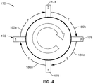
- FIG. 4 depicts a 4-port circulator symbol 170 which represents the wave propagation behavior of the four port device in which waves launched into the structure only travel clockwise to the next port with a time delay of T.
- the symbol is shown with port 1 172 with a delay/transmission line 180a represented with delay T reaching port 2 174, that has a delay/transmission line 180b with delay T reaching port 3 176, that has a delay/transmission line 180c with delay T reaching port 4 178, that has a delay/transmission line 180d with delay T reaching port 1 172.
- the three-port circulator can be considered as a special case of the four-port circulator with port 4 178 is being open, while the two-port gyrator can thus be derived by opening circuits on both port 3 176 and port 4 178.
- the circulator concept is valid at frequencies above the low Kilohertz range (e.g., > 5 KHz) to any frequency assuming switches and delay lines operating at those frequencies are available, which means hundreds of Gigahertz to the Terahertz range and even into the visible light regime.
- a high switching frequency implies that a short delay line can be used which is suitable for on-chip integration.
- the switching speed (speed of turning on and off) of the switches is crucial to device performance as faster switches will incur less switching noise caused by the blanking of the signal during the transition time.
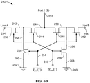
- FIG. 5A and FIG. 5B illustrate two example embodiments 190, 230 (reference designs) of an RF SPDT switch showing interconnected transistors.
- the switch provides a short circuit to the transmission lines when turned off and the switch in FIG. 5B provides open circuit reflection to the ports that are turned off.
- port 1 192 is the common line (connection) of the switch and is seen connecting into line 212 between transistors 208, 214, which respectively connect to switched line 194 and switched line 196, respectively.
- a first shunt transistor 200 is shown coupling through connection 198 to line 194, then from transistor 200 through connection 202 to ground 204, with a second shunt transistor 218 coupling through connection 216 to line 196, and from transistor 218 through connection 220 to ground 222.
- a control signal V sw (t) 210 is seen coupled to the gates of transistors 208, 218, while the inverse signal V sw (t)' 206 is seen coupled to the gates of transistors 200 and 214. It will be appreciated that V sw (t) with its inverse signal are readily obtained from differential control outputs.
- FIG. 5B the circuit is similar to that of FIG. 5A , but utilizes additional transistors to isolate the non-selected switched output, instead of shorting it to ground.
- Port 1 232 is the common connection for the switch and connects into line 246 between transistors 244, 248 which control switch selection.
- Another transistor 238 is coupled by connection 242 outboard of transistor 244, with a counterpart transistor 252 coupled by connection 250 outboard of transistor 248.
- the outward side of transistor 238 is connected to switched output 234, while the outward side of transistor 252 is connected to switched output 236.
- a first shunt transistor 258 is shown coupling through connection 256 to line 242, then from transistor 258 through connection 260 to ground 262, with a second shunt transistor 266 coupling through connection 264 to line 250, and from transistor 266 through connection 268 to ground 269.
- V sw (t) 240 is seen coupled to the gates of transistors 238, 244 and 266, while its inverse signal V sw (t)' 254 is seen coupled to the gates of transistors 248, 252 and 258. It will be appreciated that V sw (t) with its inverse counterpart are readily obtained from differential control outputs.
- FIG. 5A or FIG. 5B can be utilized in the 2-port device of FIG. 1A and the 3-port device in FIG. 2A .
- FIG. 6 illustrates an example embodiment of a DPDT switch comprising a cross-connection of two open circuit SPDT switches (e.g., FIG. 5B ), which may be utilized for creating DPDT switches as utilized in FIG. 2A and FIG. 3A .
- Connection 280 is coupled from switched connection 276 (Line A) to transistor 282 which is coupled through connection 286 to transistor 288 whose output connects 287 to common line 272 (Port 1, 2).
- Connection 290 is coupled from first common connection 272 (Port 1, 2) to transistor 292 which is coupled through connection 296 to transistor 298 whose output 300 connects to switched line 278 (Line B).
- Connection 302 is coupled from switched connection 278 (Line B) to transistor 304 which is coupled through connection 308 to transistor 310 whose output connects 312 to second common line 274 (Port 3, 4).
- Connection 314 is coupled from second common lines 274 (Port 3, 4) to transistor 316 which is coupled through connection 320 to transistor 322 whose output 323 connects to switched line 276 (Line A).
- the shunt circuits are seen interior of this circuit connecting to ground 328.
- the first side of transistor 324 is connected 326 to line 286 with its opposing side connected to ground 328.
- the first side of transistor 332 is connected 330 to line 296 with its opposing side connected to ground 328.
- the first side of transistor 338 is connected 336 to line 308 with its opposing side connected to ground 328.
- the first side of transistor 344 is connected 342 to line 320 with its opposing side connected to ground 328.
- a control signal V sw (t) 284a, 284b is seen coupled to the gates of transistors 282, 288, 332, 304, 310 and 344, while the inverse signal V sw (t)' 318a, 318b is seen coupled to the gates of transistors 292, 298, 324, 316, 322 and 338. It will be appreciated that V sw (t) with its inverse signal are readily obtained from utilizing differentially-ended control outputs.
- the switching rate can be chosen to be higher (oversampling) or lower (undersampling) than the signal frequency.
- the former is preferred as the switching noise can be easily eliminated with the help of low pass filters placed at the ports.
- oversampling requires switch devices operating at several tens of GHz switching rate to avoid switching loss.
- the switching rate was chosen to be 3 GHz, which corresponds to an 83 ps delay on each transmission line. This corresponds to a straight length of 10 mm trace on GaN substrate and the line occupies an actual area close to 2 mm x 1 mm in view of the routing path. With two such delay lines and two transistor switches, the total area of the MMIC should readily fit in a chip area of 3 mm x 3 mm.
- Switches are assumed to have a figure of merit similar to what is offered by a typical 0.15 ⁇ m gate length GaN HEMT switch with a switch on-resistance of 5 Ohm and off-capacitance of 0.05 pF.
- FIG. 7 illustrates simulated scattering parameters 350 from port 1 to all the ports over an ultra-wide frequency band of 100 MHz to 1.5 GHz.
- the return loss S11 is shown to be lower than -25 dB over the whole band and it is limited by the return loss of the low pass filter placed at the port.
- S21 is the feed through from port 1 to port 2, which shows a low insertion loss of less than 1.5 dB over all the frequencies.
- S31 and S41 are isolation parameters from port 1 to port 3 and port 4, which both appear to be lower than 28 dB, again, limited by both the impedance match of the low pass filters at port 2 and port 3 and the isolation of the DPDT switch.
- the only power consumption is that of driving the gates of the transistor switches, which should be in the range of a few milliwatts if the aforementioned GaN HEMT devices are used.
- a general approach of realizing passive, non-reciprocal devices including a two-port gyrator, three-port and four-port circulators based on SSDL has been disclosed.
- the non-reciprocity of the disclosed devices is achieved over an ultra-wide band, such as from DC to RF.
- Theoretical models of the non-reciprocity and enabling switching technologies have been discussed. Simulation results validate the approach of the SSDL disclosure.
- the disclosed SSDL devices may find broad applications in RF front-ends for wireless communications, radar and sensors to protect the receiver from being interfered with by transmitter leakage or to develop novel devices and applications that utilize such broadband non-reciprocity.
- a set refers to a collection of one or more objects.
- a set of objects can include a single object or multiple objects.
- the terms “substantially” and “about” are used to describe and account for small variations.
- the terms can refer to instances in which the event or circumstance occurs precisely as well as instances in which the event or circumstance occurs to a close approximation.
- the terms can refer to a range of variation of less than or equal to ⁇ 10% of that numerical value, such as less than or equal to ⁇ 5%, less than or equal to ⁇ 4%, less than or equal to ⁇ 3%, less than or equal to ⁇ 2%, less than or equal to ⁇ 1 %, less than or equal to ⁇ 0.5%, less than or equal to ⁇ 0.1 %, or less than or equal to ⁇ 0.05%.
- substantially aligned can refer to a range of angular variation of less than or equal to ⁇ 10°, such as less than or equal to ⁇ 5°, less than or equal to ⁇ 4°, less than or equal to ⁇ 3°, less than or equal to ⁇ 2°, less than or equal to ⁇ 1°, less than or equal to ⁇ 0.5°, less than or equal to ⁇ 0.1°, or less than or equal to ⁇ 0.05°.
- range format is used for convenience and brevity and should be understood flexibly to include numerical values explicitly specified as limits of a range, but also to include all individual numerical values or sub-ranges encompassed within that range as if each numerical value and sub-range is explicitly specified.
- a ratio in the range of about 1 to about 200 should be understood to include the explicitly recited limits of about 1 and about 200, but also to include individual ratios such as about 2, about 3, and about 4, and sub-ranges such as about 10 to about 50, about 20 to about 100, and so forth.
- Sequentially-Switched Delay Line can realize passive, nonmagnetic and non-reciprocal components for electromagnetic waves over ultra-wideband through the breaking of the time-reversal symmetry.
- a SSDL structure with six sections of transmission lines and five Single Pole Double Throw (SPDT) switches has been proposed as a three-port circulator in the literature.
- SPDT Single Pole Double Throw
- a simpler structure consisting of only two sections of transmission lines with two switches is proposed, which can operate as a two-port non-reciprocal phase shifter (gyrator) with two SPDT switches, a three-port circulator with one DPDT switch and one SPDT switch, or a four-port circulator with two DPDT switches.
- Simulation results for one design at radio frequency demonstrated the expected non-reciprocal behavior from DC to 1.5GHz for aforementioned three configurations.
Landscapes
- Physics & Mathematics (AREA)
- Nonlinear Science (AREA)
- Engineering & Computer Science (AREA)
- Computer Networks & Wireless Communication (AREA)
- General Physics & Mathematics (AREA)
- Radar, Positioning & Navigation (AREA)
- Remote Sensing (AREA)
- Signal Processing (AREA)
- Waveguide Switches, Polarizers, And Phase Shifters (AREA)
- Transceivers (AREA)
- Radar Systems Or Details Thereof (AREA)
Abstract
Description
- This application claims priority to, and the benefit of,
U.S. provisional patent application serial number 62/452,818 filed on January 31, 201715/692,091 filed August 31, 2017 - The technology presented herein includes but is not limited to two-port, three-port and four-port non-reciprocal devices with sequentially switched delay lines (SSDL) in original form.
- A portion of the material in this patent document may be subject to copyright protection under the copyright laws of the United States and of other countries. The owner of the copyright rights has no objection to the facsimile reproduction by anyone of the patent document or the patent disclosure, as it appears in the United States Patent and Trademark Office publicly available file or records, but otherwise reserves all copyright rights whatsoever. The copyright owner does not hereby waive any of its rights to have this patent document maintained in secrecy, including without limitation its rights pursuant to 37 C.F.R. § 1.14.
- The technology of this disclosure pertains generally to non-reciprocal components, and more particularly to non-reciprocal sequentially-switched delay line (SSDL) gyrators and circulators.
- Reciprocity is generally observed in passive components fabricated from electric material due to the time-reversal symmetry of the material property. In the past passive non-reciprocal components could only be realized by use of non-reciprocal magnetic material, which is often narrow band, bulky, expensive and is not compatible with modern integrated circuit process.
- More recently, active circulators implemented with transistors have been realized based on the non-reciprocal transfer behavior of transistors. In comparison with traditional circulators, these circulators offer smaller physical size and have greater compatibility with integrated circuit (IC) technology.
- However, as in many other transistor based devices, active circulators tend to suffer from noise issues and have limited power performance. These shortcomings often prevent active circulators from being utilized in systems requiring wide dynamic range. Non-reciprocity has been realized through modulating the dielectric property of a transmission line in time and space to break the time reversal symmetry. For RF applications, a time-modulation architecture has been applied to a parametrically coupled resonator and a commutating switched capacitor device to achieve magnetless non-reciprocity, yet with an isolation bandwidth which is intrinsically narrow.
- In addition, broadband isolation at RF frequencies has been demonstrated on a Monolithic Microwave Integrated Circuit (MMIC) based on Time-Varying Transmission Line (TVTL). However, despite the ability to offer broadband isolation, its lowest operating frequency is dictated by the longest delay of the TVTL that can be implemented on chip, thus resulting in a large chip area for low RF frequencies. Furthermore, the extent of isolation of the TVTL isolator over a broad bandwidth is also limited by a SINC function.
- Toward achieving non-reciprocity without limiting the lower bound of operating frequency, Sequentially-Switched Delay Line (SSDL) devices were developed to create a passive circulator over a very broad frequency range from almost DC to RF. The SSDLs combine time-reversal symmetry breaking with multiplexing/demultiplexing offered by high-speed switches to route the waves traveling in opposite directions to different ports in a seamless manner. The time switching strategy emulates real-time traffic control with no theoretical bandwidth limit. A circulator can thus be built allowing simultaneous transmit and receive (STAR) of the electromagnetic waves without stops or reflections, yet providing theoretically infinite isolation between the two.
- Accordingly, a need exists for SSDL devices which can be implemented with reduced components counts and sizes toward minimizing integrated circuit real estate.
- A possible solution is described to the problem of separating simultaneous transmit and receive signals at the same frequency in wireless communication systems or radar/sensor systems, to protect the receiver being interfered with by the transmitter.
- The technology is based on sequentially turning on and off of the switches that are connected to multiple segments of delay lines. The approach is similar one's daily experience that one-way traffic synchronized with the turning on of multiple green lights can pass all the way without stopping, but the traffic in the other direction will experience delay. The technology offers a true passive solution than can enable circulators to be fabricated on-chip for operation in a frequency range (e.g., just above DC to the frequency of light).
- The technology offers a practical, robust and cost efficient way of implementing high performance circulators that can be integrated on chip. The technology can be implemented in basically any wireless transmitters and radar sensor systems that require reciprocity.
- Further aspects of the technology described herein will be brought out in the following portions of the specification, wherein the detailed description is for the purpose of fully disclosing preferred embodiments of the technology without placing limitations thereon.
- The technology described herein will be more fully understood by reference to the following drawings which are for illustrative purposes only:
-
FIG. 1A and FIG. 1B are a schematic and associated switch control signals of a 2-port non-reciprocal phase shifter (gyrator) based on SSDL, according to an embodiment of the present disclosure. -
FIG. 2A and FIG. 2B are a schematic and associated switch control signals of a 3-port circulator based on SSDL, according to an embodiment of the present disclosure. -
FIG. 3A and FIG. 3B are a schematic and associated switch control signals of a 4-port circulator based on SSDL, according to an embodiment of the present disclosure. -
FIG. 4 is a representative symbol utilized for the 4-port circulator showing clockwise port transfer characteristics, according to an embodiment of the present disclosure. -
FIG. 5A andFIG. 5B are schematic diagrams of transistorized SPDT switches shown inFIG. 5A with short circuit reflection when turned off, and inFIG. 5B with switches having open circuit reflection when turned off, according to embodiments of the present disclosure. -
FIG. 6 is a schematic of an example DPDT switch designed with transistors that can be utilized in the three-port and four-port circulators, according to an embodiment of the present disclosure. -
FIG. 7 is a plot of simulated S parameters fromport 1 to all the ports over frequency range from 100 MHz to 1.5 GHz, as determined for an embodiment of the present disclosure. - The present disclosure describes general realizations of non-reciprocal devices based on SSDL including two-port non-reciprocal phase shifters (gyrators), three-port circulators and four-port circulators. The proposed non-reciprocal devices are based on a simpler structure than those found in the current state of the art, as the disclosed devices require just two sections of transmission lines and two switches. Benefits from utilizing these simplified structures include reduced chip area and lower insertion loss in on-chip implementations.
-
FIG. 1A and FIG. 1B illustrate an example embodiment of a two-port non-reciprocal phase shifters, showing a schematic ofembodiment 10 inFIG. 1A and a switch control diagram 30 seen inFIG. 1B . - In
FIG. 1A thenon-reciprocal phase shifter 10 has a first port 12 asecond port 14 and comprises two identical sections oftransmission lines T. First port 12 is coupled through the common line on anSPDT switch 16 to select betweenlines Lines transmission line segments connections switch 26, whose state is controlled by signal Vsw2(t) = Vsw1(t -T) 28, with the common connection of the switch coupled tosecond port 14. - Thus, the two SPDT switches perform switching between these two lines. In particular, it is seen that a signal at
port 1 can be directed byswitch 16 totransmission line switch 26 then selecting whether to connect to 22a or 22b, which is directed tosecond port 14. It should also be appreciated that although the above described a single signal direction of travel, the device embodiment ofFIG. 1A as well as the other embodiments are bi-directional; which is to say they control signal movement in both directions. - In
FIG. 1B is seen thesignals 30 for controlling switching of Vsw1(t) 18 seen in the upper waveform, and switching of Vsw2(t) 28 in the lower waveform. The switches are controlled by the use of substantially rectangular waveforms that have a period of 4T, with a bi-level voltage selecting the connection to either line A (VA) or line B (VB). Within each period, the switches connect the two ports to one of the two transmission lines, e.g.,line A 22a, for a time duration of 2T before they are switched to the other line, e.g.,line B 22b for another 2T. - Denoting the port at the left as
port 1 12 and the one at the right asport 2 14, one may select the switching pattern shown inFIG. 1A so thatport 2 is connected to the same line withport 1 always behind a fixed time of T. The electromagnetic wave launched intoport 1 is split into two pulses with a duration of 2T that are propagating on the two lines respectively. Each pulse propagates on one of the transmission lines. This pulse requires a time duration of T to arrive at the end of that line next toport 2, at which moment the switch is turned to that line to connect it toport 2. Therefore, the two split pulses are combined atport 2 without loss of the information or enduring an extra delay. On the contrary, if the wave is launched intoport 2, the pulses will arrive at the end of the line next toport 1 when the switch is turned away, disconnecting that line fromport 1. Therefore, this pulse launched intoport 2 will be reflected by theport 1 switch, traveling back toport 2 and being reflected once again by theport 2 switch, traveling towardport 1 again and finally arriving atport 1 after a time duration of 3T. Therefore, one may express the voltage transfer relationship betweenport 
- It is thus evident from Eq. 1 that a non-reciprocal phase shifter/delay line or gyrator is created with the SSDL structure shown in
FIG. 1A . -
FIG. 2A through FIG. 2B illustrates an example three-port circulator embodiment 50 withexample switching waveforms 90. To create a three-port circulator, the SPDT switch atport 1 12 fromFIG. 1A is replaced with a DPDT switch that forms the third port.Port 1 52 andport 3 56 connections are each seen split into two lines which are coupled to aDPDT switch 58, comprising two interconnected SPDT switches shown as afirst switch 60a and asecond switch 60b, whose state is both switched in response to signal 62 Vsw1(t).Switch 60a hasoutput 64a, withswitch 60b having output 64b, with these outputs coupled to transmission lines A 66a, andB 66b, respectively.Connections port 2 54. The state of switch 70 is controlled in response to the signal Vsw2(t) = Vsw1(t -T) 72. - It will be appreciated that the DPDT switch interconnects the two SPDT switches so that when the switch is in a first state,
port 1 52 couples totransmission line A 66a withport 3 56 coupling totransmission line 66b. In a second switch state,port 1 52 couples totransmission line B 66b withport 3 56 coupling totransmission line A 66a. - The wave launched into
port 2 54 now travels toport 3 56 through theDPDT switch 58 with a time delay of T, instead of being reflected by the SPDT next toport 1 52. However, a wave launched intoport 3 still experiences reflection at the SPDT next toport 2 54 and finally arrives atport 1 after a time delay of 2T. InFIG. 2B is shown an embodiment ofcontrol waveforms 90, showing Vsw1(t) and Vsw2(t), and the periods T of the rectangular waveforms. - Thus, this embodiment results in one-half of the delay and a much simpler structure than found in current devices. The voltage transfer relationship for this three port device is summarized as follows,

-
FIG. 3A and FIG. 3B illustrate an example four-port circulator embodiment 110 withexample switching waveforms 150.Port 1 112 andport 3 116 are each seen split into two lines which are coupled toDPDT switch 120, as was seen inFIG. 2A , which comprises two interconnected SPDT switches shown as afirst switch 122a and asecond switch 122b, whose state is both switched in response to signal Vsw1(t) 124.Common connections DPDT switch 120 are coupled totransmission line A 128a, andtransmission line B 128b.Connections B 128b, connect to common connections of anotherDPDT switch 132, comprisinginterconnected SPDT switches DPDT switch 132 is both controlled by signal Vsw2(t) = Vsw1(t-T) 134, which is seen inFIG. 3B . The four switched outputs fromDPDT switch 132 are combined and connected toport 2 114 andport 4 118. In a first state ofswitch 132,transmission line A 128a is coupled toport 2 114 whiletransmission line B 128b is coupled toport 4 118. In a second state ofswitch 132,transmission line A 128a is coupled toport 4 118 whiletransmission line B 128b is coupled toport 2 114. - In
FIG. 3B is shown an embodiment ofcontrol waveforms 150, showing Vsw1(t) and Vsw2(t), and the periods T of the rectangular waveforms, which can be the same as utilized for controlling the devices ofFIG. 1A andFIG. 2A . - The above example provides a further extension of the three-port device to a four-port device, by replacing the remaining SPDT switch with a DPDT switch, to arrive at a physically symmetrical devices. Under the same sequential switching pattern, it can be easily derived that this device operates as a four-port circulator with the following voltage transfer relationship,

- It should be appreciated that the delay among the four ports are completely symmetrical now.
-
FIG. 4 depicts a 4-port circulator symbol 170 which represents the wave propagation behavior of the four port device in which waves launched into the structure only travel clockwise to the next port with a time delay of T. The symbol is shown withport 1 172 with a delay/transmission line 180a represented with delayT reaching port 2 174, that has a delay/transmission line 180b with delayT reaching port 3 176, that has a delay/transmission line 180c with delayT reaching port 4 178, that has a delay/transmission line 180d with delayT reaching port 1 172. - The three-port circulator can be considered as a special case of the four-port circulator with
port 4 178 is being open, while the two-port gyrator can thus be derived by opening circuits on bothport 3 176 andport 4 178. - It is worth noting that there is no absolute requirement of either switching time or delay length enforced by the Sequentially-Switched Delay Line (SSDL) operation except the synchronization between the two. In theory, the circulator concept is valid at frequencies above the low Kilohertz range (e.g., > 5 KHz) to any frequency assuming switches and delay lines operating at those frequencies are available, which means hundreds of Gigahertz to the Terahertz range and even into the visible light regime. A high switching frequency implies that a short delay line can be used which is suitable for on-chip integration. The switching speed (speed of turning on and off) of the switches is crucial to device performance as faster switches will incur less switching noise caused by the blanking of the signal during the transition time.
-
FIG. 5A andFIG. 5B illustrate twoexample embodiments 190, 230 (reference designs) of an RF SPDT switch showing interconnected transistors. InFIG. 5A the switch provides a short circuit to the transmission lines when turned off and the switch inFIG. 5B provides open circuit reflection to the ports that are turned off. - In
FIG. 5A port 1 192 is the common line (connection) of the switch and is seen connecting intoline 212 betweentransistors line 194 and switchedline 196, respectively. Afirst shunt transistor 200 is shown coupling throughconnection 198 toline 194, then fromtransistor 200 throughconnection 202 toground 204, with asecond shunt transistor 218 coupling throughconnection 216 toline 196, and fromtransistor 218 throughconnection 220 toground 222. A control signal Vsw(t) 210 is seen coupled to the gates oftransistors transistors - In
FIG. 5B the circuit is similar to that ofFIG. 5A , but utilizes additional transistors to isolate the non-selected switched output, instead of shorting it to ground. -
Port 1 232 is the common connection for the switch and connects intoline 246 betweentransistors 244, 248 which control switch selection. Anothertransistor 238 is coupled byconnection 242 outboard of transistor 244, with acounterpart transistor 252 coupled byconnection 250 outboard oftransistor 248. The outward side oftransistor 238 is connected to switchedoutput 234, while the outward side oftransistor 252 is connected to switchedoutput 236. Afirst shunt transistor 258 is shown coupling throughconnection 256 toline 242, then fromtransistor 258 throughconnection 260 toground 262, with asecond shunt transistor 266 coupling throughconnection 264 toline 250, and fromtransistor 266 throughconnection 268 toground 269. A control signal Vsw(t) 240 is seen coupled to the gates oftransistors transistors - It should be appreciated that either
FIG. 5A orFIG. 5B can be utilized in the 2-port device ofFIG. 1A and the 3-port device inFIG. 2A . -
FIG. 6 illustrates an example embodiment of a DPDT switch comprising a cross-connection of two open circuit SPDT switches (e.g.,FIG. 5B ), which may be utilized for creating DPDT switches as utilized inFIG. 2A andFIG. 3A . - In the figure is seen the first and second
common lines connections Connection 280 is coupled from switched connection 276 (Line A) totransistor 282 which is coupled throughconnection 286 totransistor 288 whose output connects 287 to common line 272 (Port 1, 2).Connection 290 is coupled from first common connection 272 (Port 1, 2) totransistor 292 which is coupled throughconnection 296 totransistor 298 whoseoutput 300 connects to switched line 278 (Line B).Connection 302 is coupled from switched connection 278 (Line B) totransistor 304 which is coupled throughconnection 308 totransistor 310 whose output connects 312 to second common line 274 (Port 3, 4).Connection 314 is coupled from second common lines 274 (Port 3, 4) totransistor 316 which is coupled throughconnection 320 totransistor 322 whoseoutput 323 connects to switched line 276 (Line A). - The shunt circuits are seen interior of this circuit connecting to
ground 328. The first side oftransistor 324 is connected 326 toline 286 with its opposing side connected toground 328. The first side oftransistor 332 is connected 330 toline 296 with its opposing side connected toground 328. The first side oftransistor 338 is connected 336 toline 308 with its opposing side connected toground 328. The first side oftransistor 344 is connected 342 toline 320 with its opposing side connected toground 328. - A control signal Vsw(t) 284a, 284b is seen coupled to the gates of
transistors transistors - The switching rate can be chosen to be higher (oversampling) or lower (undersampling) than the signal frequency. The former is preferred as the switching noise can be easily eliminated with the help of low pass filters placed at the ports. For signals at around 1 GHz, however, oversampling requires switch devices operating at several tens of GHz switching rate to avoid switching loss. For an on-chip implementation, in at least one example embodiment the following design parameters were chosen by way of example and not limitation. The switching rate was chosen to be 3 GHz, which corresponds to an 83 ps delay on each transmission line. This corresponds to a straight length of 10 mm trace on GaN substrate and the line occupies an actual area close to 2 mm x 1 mm in view of the routing path. With two such delay lines and two transistor switches, the total area of the MMIC should readily fit in a chip area of 3 mm x 3 mm.
- ADS transient circuit simulation was carried out to validate the disclosed circulator embodiments. Switches are assumed to have a figure of merit similar to what is offered by a typical 0.15 µm gate length GaN HEMT switch with a switch on-resistance of 5 Ohm and off-capacitance of 0.05 pF.
-
FIG. 7 illustratessimulated scattering parameters 350 fromport 1 to all the ports over an ultra-wide frequency band of 100 MHz to 1.5 GHz. It will be noted that the simulated isolation and insertion loss results are shown in the figure show a very flat, greater than 25dB, isolation is obtained along with insertion losses less than about 1.6 dB for frequencies from 100 MHz to 1.5 GHz. The return loss S11 is shown to be lower than -25 dB over the whole band and it is limited by the return loss of the low pass filter placed at the port. S21 is the feed through fromport 1 toport 2, which shows a low insertion loss of less than 1.5 dB over all the frequencies. S31 and S41 are isolation parameters fromport 1 toport 3 andport 4, which both appear to be lower than 28 dB, again, limited by both the impedance match of the low pass filters atport 2 andport 3 and the isolation of the DPDT switch. - Due to the symmetry of the physical structure, it is not difficult to derive the rest of the scattering parameters, which should follow the same pattern as depicted in the figure. As only passive switches are involved in the operation, the only power consumption is that of driving the gates of the transistor switches, which should be in the range of a few milliwatts if the aforementioned GaN HEMT devices are used.
- A general approach of realizing passive, non-reciprocal devices including a two-port gyrator, three-port and four-port circulators based on SSDL has been disclosed. The non-reciprocity of the disclosed devices is achieved over an ultra-wide band, such as from DC to RF. Theoretical models of the non-reciprocity and enabling switching technologies have been discussed. Simulation results validate the approach of the SSDL disclosure. The disclosed SSDL devices may find broad applications in RF front-ends for wireless communications, radar and sensors to protect the receiver from being interfered with by transmitter leakage or to develop novel devices and applications that utilize such broadband non-reciprocity.
- From the description herein, it will be appreciated that the present disclosure encompasses multiple embodiments which include, but are not limited to, the following:
- 1. A non-reciprocal apparatus with multiple ports and sequentially switched delay lines (SSDL), comprising: (a) two transmission line segments, operating as sequentially switched delay lines (SSDL), comprising a first transmission line segment and a second transmission line segment; (b) two active switches comprising a first active switch coupled to proximal ends of said first transmission line segment and second transmission line segment, and a second active switch coupled to distal ends of said first transmission line segment and second transmission line segment; (c) wherein each active switch is configured as at least one port; and (d) wherein said two active switches are configured for switching between said two transmission line segments for a selected time duration before they are switched to the other transmission line for the selected time duration, so that apparatus sequentially turns on and off said two active switches connected to multiple segments of delay lines.
- 2. A non-reciprocal apparatus with multiple ports and sequentially switched delay lines (SSDL), comprising: (a) two transmission line segments, operating as sequentially switched delay lines (SSDL), comprising a first transmission line segment and a second transmission line segment; (b) two active switches comprising a first active switch coupled to proximal ends of said first transmission line segment and second transmission line segment, and a second active switch coupled to distal ends of said first transmission line segment and second transmission line segment; (c) wherein each active switch is configured as either a single-pole double-throw (SPDT), switch, or as double-pole double-throw (DPDT) switch, with each switch having one or two port outputs; (d) wherein said two active switches are configured for switching between said two transmission line segments for a selected time duration before they are switched to the other transmission line for the selected time duration, so that apparatus sequentially turns on and off said two active switches connected to multiple segments of delay lines; and (e) a control circuit for generating switching control signals to each of said active switches.
- 3. A non-reciprocal phase shifter, gyrator, apparatus having two ports and sequentially switched delay lines (SSDL), comprising: (a) two transmission line segments, operating as sequentially switched delay lines (SSDL), comprising a first transmission line segment and a second transmission line segment; (b) two active switches comprising single-pole double-throw (SPDT) switches, with a first active switch coupled to proximal ends of said first transmission line segment and second transmission line segment, and a second active switch coupled to distal ends of said first transmission line segment and second transmission line segment; (c) wherein said two active switches are configured for switching between said two transmission line segments for a selected time duration before they are switched to the other transmission line for the selected time duration, so that apparatus sequentially turns on and off said two active switches connected to multiple segments of delay lines; and (d) a control circuit for generating switching control signals to each of said active switches.
- 4. A non-reciprocal three-port circulator apparatus using sequentially switched delay lines (SSDL), comprising: (a) two transmission line segments, operating as sequentially switched delay lines (SSDL), comprising a first transmission line segment and a second transmission line segment; (b) two active switches comprising a single-pole double-throw (SPDT) switch with a single port output and a double-pole double-throw (DPDT) switch having two port outputs; (c) wherein said two active switches comprise a first active switch coupled to proximal ends of said first transmission line segment and second transmission line segment, and a second active switch coupled to distal ends of said first transmission line segment and second transmission line segment; (d) wherein said two active switches are configured for switching between said two transmission line segments for a selected time duration before they are switched to the other transmission line for the selected time duration, so that apparatus sequentially turns on and off said two active switches connected to multiple segments of delay lines; and (e) a control circuit for generating switching control signals to each of said active switches.
- 5. A non-reciprocal four-port circulator apparatus having four ports and coupled to sequentially switched delay lines (SSDL), comprising: (a) two transmission line segments, operating as sequentially switched delay lines (SSDL), comprising a first transmission line segment and a second transmission line segment; (b) two active switches comprising double-pole double-throw (DPDT) switches each having two port outputs, in which said two active switches comprise a first active switch coupled to proximal ends of said first transmission line segment and second transmission line segment, and a second active switch coupled to distal ends of said first transmission line segment and second transmission line segment; (c) wherein said two active switches are configured for switching between said two transmission line segments for a selected time duration before they are switched to the other transmission line for the selected time duration, so that apparatus sequentially turns on and off said two active switches connected to multiple segments of delay lines; and (d) a control circuit for generating switching control signals to each of said active switches.
- 6. The apparatus as recited in any preceding or following embodiment, further comprising a control circuit for generating switching control signals to each of said active switches.
- 7. The apparatus as recited in any preceding or following embodiment, wherein said control circuit is configured for controlling said two active switches using rectangular waves that have a selected period, with a bi-level voltage selecting the connection to either said first transmission line segment, or said second transmission line segment.
- 8. The apparatus as recited in any preceding or following embodiment, wherein said apparatus is configured with multiple ports comprising two, three, or four ports.
- 9. The apparatus as recited in any preceding or following embodiment, wherein said apparatus has two-ports and is configured to operate as a non-reciprocal phase shifter (gyrator).
- 10. The apparatus as recited in any preceding or following embodiment, wherein said apparatus has three or four ports and is configured to operate as a three-port circulator or a four-port circulator.
- 11. The apparatus as recited in any preceding or following embodiment, wherein said apparatus separates simultaneous transmit and receive signals at a same frequency in wireless communication systems or radar/sensor systems, to protect a receiver from being interfered with by a transmitter.
- 12. The apparatus as recited in any preceding or following embodiment, wherein said apparatus is configured for operation at frequencies above 5 kHz.
- 13. The apparatus as recited in any preceding or following embodiment, wherein said apparatus is configured to provide simultaneous transmit and receive (STAR) of electromagnetic waves without stops or reflections, while providing isolation between the two.
- 14. The apparatus as recited in any preceding or following embodiment, wherein at least one of said active switches is a single-pole-double-throw (SPDT) switch coupling between a single port and said two transmission line segments.
- 15. The apparatus as recited in any preceding or following embodiment, wherein said SPDT switch comprises multiple transistors that either provide short circuit reflection when switched off, or provide open circuit reflection when turned off.
- 16. The apparatus as recited in any preceding or following embodiment, wherein at least one of said active switches is a double-pole-double-throw (DPDT) switch coupling between two ports and said two transmission line segments.
- 17. The apparatus as recited in any preceding or following embodiment, wherein said DPDT switch comprises multiple transistors that either provide short circuit reflection when switched off, or provide open circuit reflection when turned off.
- 18. The apparatus as recited in any preceding or following embodiment, wherein said control circuit is configured for controlling said two active switches using rectangular waves that have a selected period, with a bi-level voltage selecting the connection to either said first transmission line segment, or said second transmission line segment.
- 19. The apparatus as recited in any preceding or following embodiment, wherein said apparatus is configured with multiple ports comprising two, three, or four ports.
- 20. The apparatus as recited in any preceding or following embodiment, wherein said SPDT switch comprises multiple transistors that either provide short circuit reflection when switched off, or provide open circuit reflection when turned off.
- 21. The apparatus as recited in any preceding or following embodiment, wherein said DPDT switch comprises multiple transistors that either provide short circuit reflection when switched off, or provide open circuit reflection when turned off.
- 22. The apparatus as recited in any preceding or following embodiment, wherein said two active switches comprise single-pole double-throw (SPDT) switches and said apparatus has two-ports and is configured to operate as a non-reciprocal phase shifter (gyrator).
- 23. The apparatus as recited in any preceding or following embodiment, wherein said active switches comprise a single-pole double-throw (SPDT) switch and a double-pole double-throw (DPDT) and the apparatus has three ports and is configured to operate as a three-port circulator.
- 24. The apparatus as recited in any preceding or following embodiment, wherein said active switches comprise a single-pole double-throw (SPDT) switch and a double-pole double-throw (DPDT) switch, and the apparatus has three ports and is configured to operate as a three-port circulator.
- 25. The apparatus as recited in any preceding or following embodiment, wherein said active switches comprise two double-pole double-throw (DPDT) switches, and the apparatus has four ports and is configured to operate as a four-port circulator.
- 26. The apparatus as recited in any preceding or following embodiment, wherein said apparatus is configured to provide simultaneous transmit and receive (STAR) of electromagnetic waves without stops or reflections, while providing isolation between the two.
- As used herein, the term "set" refers to a collection of one or more objects. Thus, for example, a set of objects can include a single object or multiple objects.
- As used herein, the terms "substantially" and "about" are used to describe and account for small variations. When used in conjunction with an event or circumstance, the terms can refer to instances in which the event or circumstance occurs precisely as well as instances in which the event or circumstance occurs to a close approximation. When used in conjunction with a numerical value, the terms can refer to a range of variation of less than or equal to ± 10% of that numerical value, such as less than or equal to ±5%, less than or equal to ±4%, less than or equal to ±3%, less than or equal to ±2%, less than or equal to ±1 %, less than or equal to ±0.5%, less than or equal to ±0.1 %, or less than or equal to ±0.05%. For example, "substantially" aligned can refer to a range of angular variation of less than or equal to ±10°, such as less than or equal to ±5°, less than or equal to ±4°, less than or equal to ±3°, less than or equal to ±2°, less than or equal to ±1°, less than or equal to ±0.5°, less than or equal to ±0.1°, or less than or equal to ±0.05°.
- Additionally, amounts, ratios, and other numerical values are sometimes presented herein in a range format. It is to be understood that such range format is used for convenience and brevity and should be understood flexibly to include numerical values explicitly specified as limits of a range, but also to include all individual numerical values or sub-ranges encompassed within that range as if each numerical value and sub-range is explicitly specified. For example, a ratio in the range of about 1 to about 200 should be understood to include the explicitly recited limits of about 1 and about 200, but also to include individual ratios such as about 2, about 3, and about 4, and sub-ranges such as about 10 to about 50, about 20 to about 100, and so forth.
- Although the description herein contains many details, these should not be construed as limiting the scope of the disclosure but as merely providing illustrations of some of the presently preferred embodiments. Therefore, it will be appreciated that the scope of the disclosure fully encompasses other embodiments which may become obvious to those skilled in the art.
- In the claims, reference to an element in the singular is not intended to mean "one and only one" unless explicitly so stated, but rather "one or more." All structural, chemical, and functional equivalents to the elements of the disclosed embodiments that are known to those of ordinary skill in the art are expressly incorporated herein by reference and are intended to be encompassed by the present claims. Furthermore, no element, component, or method step in the present disclosure is intended to be dedicated to the public regardless of whether the element, component, or method step is explicitly recited in the claims. No claim element herein is to be construed as a "means plus function" element unless the element is expressly recited using the phrase "means for". No claim element herein is to be construed as a "step plus function" element unless the element is expressly recited using the phrase "step for".
- All elements, parts and steps described herein are preferably included. It is to be understood that any of these elements, parts and steps may be replaced by other elements, parts and steps or deleted altogether as will be obvious to those skilled in the art.
- Broadly, this writing discloses at least the following: Sequentially-Switched Delay Line (SSDL) can realize passive, nonmagnetic and non-reciprocal components for electromagnetic waves over ultra-wideband through the breaking of the time-reversal symmetry. A SSDL structure with six sections of transmission lines and five Single Pole Double Throw (SPDT) switches has been proposed as a three-port circulator in the literature. In this disclosure, a simpler structure consisting of only two sections of transmission lines with two switches is proposed, which can operate as a two-port non-reciprocal phase shifter (gyrator) with two SPDT switches, a three-port circulator with one DPDT switch and one SPDT switch, or a four-port circulator with two DPDT switches. Simulation results for one design at radio frequency demonstrated the expected non-reciprocal behavior from DC to 1.5GHz for aforementioned three configurations.
Claims (15)
- A non-reciprocal apparatus with multiple ports and sequentially switched delay lines (SSDL), comprising:two transmission line segments, operating as sequentially switched delay lines (SSDL), comprising a first transmission line segment and a second transmission line segment;two active switches comprising a first active switch coupled to proximal ends of said first transmission line segment and second transmission line segment, and a second active switch coupled to distal ends of said first transmission line segment and second transmission line segment;wherein each active switch is configured as at least one port; andwherein said two active switches are configured for switching between said two transmission line segments for a selected time duration before they are switched to the other transmission line for the selected time duration, so that apparatus sequentially turns on and off said two active switches connected to multiple segments of delay lines.
- The apparatus as recited in claim 1, further comprising a control circuit for generating switching control signals to each of said active switches.
- The apparatus as recited in claim 2, wherein said control circuit is configured for controlling said two active switches using rectangular waves that have a selected period, with a bi-level voltage selecting the connection to either said first transmission line segment, or said second transmission line segment.
- The apparatus as recited in claim 1, wherein said apparatus is configured with multiple ports comprising two, three, or four ports.
- The apparatus as recited in claim 1, wherein said apparatus has two-ports and is configured to operate as a non-reciprocal phase shifter (gyrator).
- The apparatus as recited in claim 1, wherein said apparatus has three or four ports and is configured to operate as a three-port circulator or a four-port circulator.
- The apparatus as recited in claim 1, wherein said apparatus separates simultaneous transmit and receive signals at a same frequency in wireless communication systems or radar/sensor systems, to protect a receiver from being interfered with by a transmitter.
- The apparatus as recited in claim 1, wherein said apparatus is configured for operation at frequencies above 5 kHz.
- The apparatus as recited in claim 1, wherein said apparatus is configured to provide simultaneous transmit and receive (STAR) of electromagnetic waves without stops or reflections, while providing isolation between the two.
- The apparatus as recited in claim 1, wherein at least one of said active switches is a single-pole-double-throw (SPDT) switch coupling between a single port and said two transmission line segments.
- The apparatus as recited in claim 10, wherein said SPDT switch comprises multiple transistors that either provide short circuit reflection when switched off, or provide open circuit reflection when turned off.
- The apparatus as recited in claim 1, wherein at least one of said active switches is a double-pole-double-throw (DPDT) switch coupling between two ports and said two transmission line segments.
- The apparatus as recited in claim 12, wherein said DPDT switch comprises multiple transistors that either provide short circuit reflection when switched off, or provide open circuit reflection when turned off.
- The apparatus of claim 1, wherein:each active switch is configured as either a single-pole double-throw (SPDT) switch, or as double-pole double-throw (DPDT) switch, with each switch having one or two port outputs;the apparatus further comprising a control circuit for generating switching control signals to each of said active switches.
- A non-reciprocal phase shifter, gyrator, apparatus comprising: an apparatus according to claim 1, wherein:said two active switches comprise single-pole double-throw (SPDT) switchessaid apparatus further comprising a control circuit for generating switching control signals to each of said active switches.
Applications Claiming Priority (2)
| Application Number | Priority Date | Filing Date | Title |
|---|---|---|---|
| US201762452818P | 2017-01-31 | 2017-01-31 | |
| US15/692,091 US10615475B2 (en) | 2017-01-31 | 2017-08-31 | Two-port, three-port and four-port non-reciprocal devices with sequentially switched delay lines (SSDL) |
Publications (2)
| Publication Number | Publication Date |
|---|---|
| EP3355403A1 true EP3355403A1 (en) | 2018-08-01 |
| EP3355403B1 EP3355403B1 (en) | 2021-04-07 |
Family
ID=61094228
Family Applications (1)
| Application Number | Title | Priority Date | Filing Date |
|---|---|---|---|
| EP18153590.7A Active EP3355403B1 (en) | 2017-01-31 | 2018-01-26 | Multi port non-reciprocal devices with sequentially switched delay lines (ssdl) |
Country Status (5)
| Country | Link |
|---|---|
| US (1) | US10615475B2 (en) |
| EP (1) | EP3355403B1 (en) |
| KR (1) | KR102498446B1 (en) |
| CN (1) | CN108377143B (en) |
| WO (1) | WO2018144075A1 (en) |
Cited By (1)
| Publication number | Priority date | Publication date | Assignee | Title |
|---|---|---|---|---|
| US10629976B2 (en) * | 2016-04-18 | 2020-04-21 | Eagantu Ltd. | Wide band radio frequency circulator |
Families Citing this family (6)
| Publication number | Priority date | Publication date | Assignee | Title |
|---|---|---|---|---|
| CN110400998B (en) * | 2019-08-14 | 2021-06-08 | 中国人民解放军空军工程大学 | A free-space nonreciprocal transmission line structure based on active devices |
| CN111628801B (en) * | 2020-05-28 | 2022-02-01 | 维沃移动通信有限公司 | Radio frequency front-end device control method and user equipment |
| US11621465B2 (en) | 2020-06-09 | 2023-04-04 | International Business Machines Corporation | Circulator-based tunable delay line |
| CN114069178B (en) * | 2021-10-25 | 2023-04-14 | 北京理工大学 | An Integrated CMOS Circulator Based on Spatiotemporal Conductivity Modulation |
| KR102831857B1 (en) * | 2023-12-20 | 2025-07-28 | 대한민국(방위사업청장) | Spdt switch device with phase delay line |
| CN119813982B (en) * | 2024-12-19 | 2025-10-24 | 西安电子科技大学 | An ultra-wideband passive delay device |
Family Cites Families (19)
| Publication number | Priority date | Publication date | Assignee | Title |
|---|---|---|---|---|
| JPH0548560A (en) * | 1991-08-16 | 1993-02-26 | Fujitsu Ltd | Data frame delay correcting system in pcm transmission line |
| US5347239A (en) | 1992-12-03 | 1994-09-13 | Hewlett-Packard Company | Step attenuator |
| JP2901578B2 (en) * | 1997-06-27 | 1999-06-07 | 日本電気株式会社 | ATM link switching method |
| CN2382169Y (en) * | 1999-06-18 | 2000-06-07 | 陈尚仲 | Electronic switching device for universal series bus interface |
| AU2007200435B2 (en) * | 2002-02-08 | 2008-02-14 | Decode Genetics Ehf. | Method and system for defining sets by querying relational data using a set definition language |
| US6707417B2 (en) | 2002-06-11 | 2004-03-16 | Raytheon Company | Accurate range calibration architecture |
| US6686885B1 (en) | 2002-08-09 | 2004-02-03 | Northrop Grumman Corporation | Phased array antenna for space based radar |
| CN100470988C (en) * | 2002-12-16 | 2009-03-18 | 浙江中控技术股份有限公司 | Live plugging and unplugging control circuit and control method of pluggable module |
| US20050050030A1 (en) * | 2003-01-30 | 2005-03-03 | Decode Genetics Ehf. | Set definition language for relational data |
| CN2927050Y (en) * | 2006-02-07 | 2007-07-25 | 哈尔滨工业大学 | Ultrasonic phase-controlled array inspector |
| CN101017154B (en) * | 2006-02-07 | 2011-03-23 | 哈尔滨工业大学 | Ultrasonic phased array inspection instrument |
| KR100973992B1 (en) | 2006-05-25 | 2010-08-05 | 삼성전자주식회사 | Time division duplex switch in time division duplex wireless communication system |
| EP2161835B1 (en) * | 2007-01-25 | 2013-08-14 | Research In Motion Limited | System and method for filtering harmonics of a power amplifier |
| JP2008187661A (en) | 2007-01-31 | 2008-08-14 | Nec Electronics Corp | Phase shifter, and bit phase shifter |
| US9336327B2 (en) * | 2007-11-30 | 2016-05-10 | Microsoft Technology Licensing, Llc | Mapping and query translation between XML, objects, and relations |
| CA2827701A1 (en) * | 2013-09-23 | 2015-03-23 | Sureshchandra B. Patel | Methods of patel decoupled loadlow computation for electrical power system |
| CN103678593B (en) * | 2013-12-12 | 2017-09-26 | 中国科学院计算机网络信息中心 | A kind of interactive space scene search method described based on spatial scene sketch |
| CN105337540A (en) * | 2015-11-25 | 2016-02-17 | 北京金自天正智能控制股份有限公司 | Two-level circuit board for achieving permanent magnet synchronous motor frequency conversion soft start and grid-connected control |
| CN113258238B (en) | 2016-05-11 | 2022-08-26 | 加利福尼亚大学董事会 | Ultra-wideband circulator equipment |
-
2017
- 2017-08-31 US US15/692,091 patent/US10615475B2/en active Active
- 2017-10-06 WO PCT/US2017/055468 patent/WO2018144075A1/en not_active Ceased
- 2017-10-06 KR KR1020197022603A patent/KR102498446B1/en active Active
- 2017-11-20 CN CN201711158473.4A patent/CN108377143B/en active Active
-
2018
- 2018-01-26 EP EP18153590.7A patent/EP3355403B1/en active Active
Non-Patent Citations (2)
| Title |
|---|
| "Control Components Using Si,GaAs and GaN Technologies", 1 August 2014, ARTECH HOUSE, article BAHL: "Switches", XP055484742 * |
| MATHEW M. BIEDKA ET AL: "Ultra-Wide Band Non-reciprocity through Sequentially-Switched Delay Lines", SCIENTIFIC REPORTS, vol. 7, 6 January 2017 (2017-01-06), pages 40014, XP055482665, DOI: 10.1038/srep40014 * |
Cited By (1)
| Publication number | Priority date | Publication date | Assignee | Title |
|---|---|---|---|---|
| US10629976B2 (en) * | 2016-04-18 | 2020-04-21 | Eagantu Ltd. | Wide band radio frequency circulator |
Also Published As
| Publication number | Publication date |
|---|---|
| EP3355403B1 (en) | 2021-04-07 |
| US20180219269A1 (en) | 2018-08-02 |
| WO2018144075A1 (en) | 2018-08-09 |
| CN108377143B (en) | 2022-05-03 |
| US10615475B2 (en) | 2020-04-07 |
| CN108377143A (en) | 2018-08-07 |
| KR102498446B1 (en) | 2023-02-13 |
| KR20190108588A (en) | 2019-09-24 |
Similar Documents
| Publication | Publication Date | Title |
|---|---|---|
| EP3355403B1 (en) | Multi port non-reciprocal devices with sequentially switched delay lines (ssdl) | |
| US7391283B2 (en) | RF switch | |
| KR101572534B1 (en) | Radio frequency front end module and multi band module using the radio frequency front end module | |
| US10116029B2 (en) | Ultra-wide band circulators with sequentially-switched delay line (SSDL) | |
| GB2542709A (en) | Systems, circuits and methods related to low-loss bypass of a radio-frequency filter or diplexer | |
| US10637527B2 (en) | Sequentially switched bulk acoustic wave (BAW) delay line circulator | |
| CN109565268A (en) | Apparatus and method for improving Q-drop loss and phase balance in attenuator circuits | |
| JP2013141057A (en) | Front end module | |
| US11349186B2 (en) | Magnetic-free non-reciprocal circuits based on sub-harmonic spatio-temporal conductance modulation | |
| KR100848261B1 (en) | Device containing RF switch and RF switch | |
| Lin et al. | New designs of bandpass diplexer and switchplexer based on parallel-coupled bandpass filters | |
| Biedka et al. | Ultra-wide band on-chip circulator with sequentially switched delay lines (SSDL) | |
| JP2962771B2 (en) | Phase shifter | |
| US10622995B2 (en) | Independent control of branch FETs for RF performance improvement | |
| US20160197390A1 (en) | Nonreversible circuit device | |
| CN110635819B (en) | Sequentially switched Bulk Acoustic Wave (BAW) delay line circulator | |
| Ashley et al. | Non-reciprocal MMIC-based dual-band bandpass filters | |
| CN113726365B (en) | Duplexers, radio frequency communication circuits and equipment | |
| Laforge et al. | Manifold-coupled switched filter bank implementing filters with embedded switches | |
| JP2677030B2 (en) | Semiconductor phase shifter | |
| CN113852394A (en) | Filtering switch chip and wireless communication transceiver | |
| DE102004033835A1 (en) | Unit enabling use of external antenna with mobile telephone inside car, combines coaxial connection with capacitative or inductive coupling | |
| Mokerov et al. | X-band SPDT switch MMIC based on directional coupler key | |
| JPH05199014A (en) | Switch circuit | |
| JP2009219027A (en) | High-frequency multi-branch switch |
Legal Events
| Date | Code | Title | Description |
|---|---|---|---|
| PUAI | Public reference made under article 153(3) epc to a published international application that has entered the european phase |
Free format text: ORIGINAL CODE: 0009012 |
|
| STAA | Information on the status of an ep patent application or granted ep patent |
Free format text: STATUS: REQUEST FOR EXAMINATION WAS MADE |
|
| 17P | Request for examination filed |
Effective date: 20180214 |
|
| AK | Designated contracting states |
Kind code of ref document: A1 Designated state(s): AL AT BE BG CH CY CZ DE DK EE ES FI FR GB GR HR HU IE IS IT LI LT LU LV MC MK MT NL NO PL PT RO RS SE SI SK SM TR |
|
| AX | Request for extension of the european patent |
Extension state: BA ME |
|
| REG | Reference to a national code |
Ref country code: DE Ref legal event code: R079 Ref document number: 602018014950 Country of ref document: DE Free format text: PREVIOUS MAIN CLASS: H01P0001150000 Ipc: H01P0001397000 |
|
| GRAP | Despatch of communication of intention to grant a patent |
Free format text: ORIGINAL CODE: EPIDOSNIGR1 |
|
| STAA | Information on the status of an ep patent application or granted ep patent |
Free format text: STATUS: GRANT OF PATENT IS INTENDED |
|
| RIC1 | Information provided on ipc code assigned before grant |
Ipc: H01P 1/15 20060101ALI20201019BHEP Ipc: H03K 5/00 20060101ALN20201019BHEP Ipc: H01P 1/397 20060101AFI20201019BHEP Ipc: H03K 17/693 20060101ALN20201019BHEP Ipc: H03K 5/159 20060101ALI20201019BHEP Ipc: H01P 1/387 20060101ALI20201019BHEP Ipc: H01P 5/18 20060101ALI20201019BHEP |
|
| INTG | Intention to grant announced |
Effective date: 20201104 |
|
| GRAS | Grant fee paid |
Free format text: ORIGINAL CODE: EPIDOSNIGR3 |
|
| GRAA | (expected) grant |
Free format text: ORIGINAL CODE: 0009210 |
|
| STAA | Information on the status of an ep patent application or granted ep patent |
Free format text: STATUS: THE PATENT HAS BEEN GRANTED |
|
| AK | Designated contracting states |
Kind code of ref document: B1 Designated state(s): AL AT BE BG CH CY CZ DE DK EE ES FI FR GB GR HR HU IE IS IT LI LT LU LV MC MK MT NL NO PL PT RO RS SE SI SK SM TR |
|
| REG | Reference to a national code |
Ref country code: GB Ref legal event code: FG4D |
|
| REG | Reference to a national code |
Ref country code: AT Ref legal event code: REF Ref document number: 1380855 Country of ref document: AT Kind code of ref document: T Effective date: 20210415 Ref country code: CH Ref legal event code: EP |
|
| REG | Reference to a national code |
Ref country code: DE Ref legal event code: R096 Ref document number: 602018014950 Country of ref document: DE |
|
| REG | Reference to a national code |
Ref country code: IE Ref legal event code: FG4D |
|
| REG | Reference to a national code |
Ref country code: FI Ref legal event code: FGE |
|
| REG | Reference to a national code |
Ref country code: SE Ref legal event code: TRGR |
|
| REG | Reference to a national code |
Ref country code: LT Ref legal event code: MG9D |
|
| REG | Reference to a national code |
Ref country code: NL Ref legal event code: MP Effective date: 20210407 Ref country code: AT Ref legal event code: MK05 Ref document number: 1380855 Country of ref document: AT Kind code of ref document: T Effective date: 20210407 |
|
| PG25 | Lapsed in a contracting state [announced via postgrant information from national office to epo] |
Ref country code: BG Free format text: LAPSE BECAUSE OF FAILURE TO SUBMIT A TRANSLATION OF THE DESCRIPTION OR TO PAY THE FEE WITHIN THE PRESCRIBED TIME-LIMIT Effective date: 20210707 Ref country code: AT Free format text: LAPSE BECAUSE OF FAILURE TO SUBMIT A TRANSLATION OF THE DESCRIPTION OR TO PAY THE FEE WITHIN THE PRESCRIBED TIME-LIMIT Effective date: 20210407 Ref country code: HR Free format text: LAPSE BECAUSE OF FAILURE TO SUBMIT A TRANSLATION OF THE DESCRIPTION OR TO PAY THE FEE WITHIN THE PRESCRIBED TIME-LIMIT Effective date: 20210407 Ref country code: NL Free format text: LAPSE BECAUSE OF FAILURE TO SUBMIT A TRANSLATION OF THE DESCRIPTION OR TO PAY THE FEE WITHIN THE PRESCRIBED TIME-LIMIT Effective date: 20210407 Ref country code: LT Free format text: LAPSE BECAUSE OF FAILURE TO SUBMIT A TRANSLATION OF THE DESCRIPTION OR TO PAY THE FEE WITHIN THE PRESCRIBED TIME-LIMIT Effective date: 20210407 |
|
| PG25 | Lapsed in a contracting state [announced via postgrant information from national office to epo] |
Ref country code: GR Free format text: LAPSE BECAUSE OF FAILURE TO SUBMIT A TRANSLATION OF THE DESCRIPTION OR TO PAY THE FEE WITHIN THE PRESCRIBED TIME-LIMIT Effective date: 20210708 Ref country code: IS Free format text: LAPSE BECAUSE OF FAILURE TO SUBMIT A TRANSLATION OF THE DESCRIPTION OR TO PAY THE FEE WITHIN THE PRESCRIBED TIME-LIMIT Effective date: 20210807 Ref country code: NO Free format text: LAPSE BECAUSE OF FAILURE TO SUBMIT A TRANSLATION OF THE DESCRIPTION OR TO PAY THE FEE WITHIN THE PRESCRIBED TIME-LIMIT Effective date: 20210707 Ref country code: LV Free format text: LAPSE BECAUSE OF FAILURE TO SUBMIT A TRANSLATION OF THE DESCRIPTION OR TO PAY THE FEE WITHIN THE PRESCRIBED TIME-LIMIT Effective date: 20210407 Ref country code: PL Free format text: LAPSE BECAUSE OF FAILURE TO SUBMIT A TRANSLATION OF THE DESCRIPTION OR TO PAY THE FEE WITHIN THE PRESCRIBED TIME-LIMIT Effective date: 20210407 Ref country code: PT Free format text: LAPSE BECAUSE OF FAILURE TO SUBMIT A TRANSLATION OF THE DESCRIPTION OR TO PAY THE FEE WITHIN THE PRESCRIBED TIME-LIMIT Effective date: 20210809 Ref country code: RS Free format text: LAPSE BECAUSE OF FAILURE TO SUBMIT A TRANSLATION OF THE DESCRIPTION OR TO PAY THE FEE WITHIN THE PRESCRIBED TIME-LIMIT Effective date: 20210407 |
|
| REG | Reference to a national code |
Ref country code: DE Ref legal event code: R097 Ref document number: 602018014950 Country of ref document: DE |
|
| PG25 | Lapsed in a contracting state [announced via postgrant information from national office to epo] |
Ref country code: CZ Free format text: LAPSE BECAUSE OF FAILURE TO SUBMIT A TRANSLATION OF THE DESCRIPTION OR TO PAY THE FEE WITHIN THE PRESCRIBED TIME-LIMIT Effective date: 20210407 Ref country code: DK Free format text: LAPSE BECAUSE OF FAILURE TO SUBMIT A TRANSLATION OF THE DESCRIPTION OR TO PAY THE FEE WITHIN THE PRESCRIBED TIME-LIMIT Effective date: 20210407 Ref country code: RO Free format text: LAPSE BECAUSE OF FAILURE TO SUBMIT A TRANSLATION OF THE DESCRIPTION OR TO PAY THE FEE WITHIN THE PRESCRIBED TIME-LIMIT Effective date: 20210407 Ref country code: ES Free format text: LAPSE BECAUSE OF FAILURE TO SUBMIT A TRANSLATION OF THE DESCRIPTION OR TO PAY THE FEE WITHIN THE PRESCRIBED TIME-LIMIT Effective date: 20210407 Ref country code: EE Free format text: LAPSE BECAUSE OF FAILURE TO SUBMIT A TRANSLATION OF THE DESCRIPTION OR TO PAY THE FEE WITHIN THE PRESCRIBED TIME-LIMIT Effective date: 20210407 Ref country code: SM Free format text: LAPSE BECAUSE OF FAILURE TO SUBMIT A TRANSLATION OF THE DESCRIPTION OR TO PAY THE FEE WITHIN THE PRESCRIBED TIME-LIMIT Effective date: 20210407 Ref country code: SK Free format text: LAPSE BECAUSE OF FAILURE TO SUBMIT A TRANSLATION OF THE DESCRIPTION OR TO PAY THE FEE WITHIN THE PRESCRIBED TIME-LIMIT Effective date: 20210407 |
|
| PLBE | No opposition filed within time limit |
Free format text: ORIGINAL CODE: 0009261 |
|
| STAA | Information on the status of an ep patent application or granted ep patent |
Free format text: STATUS: NO OPPOSITION FILED WITHIN TIME LIMIT |
|
| 26N | No opposition filed |
Effective date: 20220110 |
|
| PG25 | Lapsed in a contracting state [announced via postgrant information from national office to epo] |
Ref country code: IS Free format text: LAPSE BECAUSE OF FAILURE TO SUBMIT A TRANSLATION OF THE DESCRIPTION OR TO PAY THE FEE WITHIN THE PRESCRIBED TIME-LIMIT Effective date: 20210807 Ref country code: AL Free format text: LAPSE BECAUSE OF FAILURE TO SUBMIT A TRANSLATION OF THE DESCRIPTION OR TO PAY THE FEE WITHIN THE PRESCRIBED TIME-LIMIT Effective date: 20210407 |
|
| PG25 | Lapsed in a contracting state [announced via postgrant information from national office to epo] |
Ref country code: IT Free format text: LAPSE BECAUSE OF FAILURE TO SUBMIT A TRANSLATION OF THE DESCRIPTION OR TO PAY THE FEE WITHIN THE PRESCRIBED TIME-LIMIT Effective date: 20210407 |
|
| PG25 | Lapsed in a contracting state [announced via postgrant information from national office to epo] |
Ref country code: MC Free format text: LAPSE BECAUSE OF FAILURE TO SUBMIT A TRANSLATION OF THE DESCRIPTION OR TO PAY THE FEE WITHIN THE PRESCRIBED TIME-LIMIT Effective date: 20210407 |
|
| REG | Reference to a national code |
Ref country code: CH Ref legal event code: PL |
|
| REG | Reference to a national code |
Ref country code: BE Ref legal event code: MM Effective date: 20220131 |
|
| PG25 | Lapsed in a contracting state [announced via postgrant information from national office to epo] |
Ref country code: LU Free format text: LAPSE BECAUSE OF NON-PAYMENT OF DUE FEES Effective date: 20220126 |
|
| PG25 | Lapsed in a contracting state [announced via postgrant information from national office to epo] |
Ref country code: BE Free format text: LAPSE BECAUSE OF NON-PAYMENT OF DUE FEES Effective date: 20220131 |
|
| PG25 | Lapsed in a contracting state [announced via postgrant information from national office to epo] |
Ref country code: LI Free format text: LAPSE BECAUSE OF NON-PAYMENT OF DUE FEES Effective date: 20220131 Ref country code: CH Free format text: LAPSE BECAUSE OF NON-PAYMENT OF DUE FEES Effective date: 20220131 |
|
| PG25 | Lapsed in a contracting state [announced via postgrant information from national office to epo] |
Ref country code: IE Free format text: LAPSE BECAUSE OF NON-PAYMENT OF DUE FEES Effective date: 20220126 |
|
| PG25 | Lapsed in a contracting state [announced via postgrant information from national office to epo] |
Ref country code: HU Free format text: LAPSE BECAUSE OF FAILURE TO SUBMIT A TRANSLATION OF THE DESCRIPTION OR TO PAY THE FEE WITHIN THE PRESCRIBED TIME-LIMIT; INVALID AB INITIO Effective date: 20180126 |
|
| PG25 | Lapsed in a contracting state [announced via postgrant information from national office to epo] |
Ref country code: MK Free format text: LAPSE BECAUSE OF FAILURE TO SUBMIT A TRANSLATION OF THE DESCRIPTION OR TO PAY THE FEE WITHIN THE PRESCRIBED TIME-LIMIT Effective date: 20210407 Ref country code: CY Free format text: LAPSE BECAUSE OF FAILURE TO SUBMIT A TRANSLATION OF THE DESCRIPTION OR TO PAY THE FEE WITHIN THE PRESCRIBED TIME-LIMIT Effective date: 20210407 |
|
| PG25 | Lapsed in a contracting state [announced via postgrant information from national office to epo] |
Ref country code: TR Free format text: LAPSE BECAUSE OF FAILURE TO SUBMIT A TRANSLATION OF THE DESCRIPTION OR TO PAY THE FEE WITHIN THE PRESCRIBED TIME-LIMIT Effective date: 20210407 |
|
| PG25 | Lapsed in a contracting state [announced via postgrant information from national office to epo] |
Ref country code: MT Free format text: LAPSE BECAUSE OF FAILURE TO SUBMIT A TRANSLATION OF THE DESCRIPTION OR TO PAY THE FEE WITHIN THE PRESCRIBED TIME-LIMIT Effective date: 20210407 |
|
| PGFP | Annual fee paid to national office [announced via postgrant information from national office to epo] |
Ref country code: SE Payment date: 20260127 Year of fee payment: 9 |
|
| PGFP | Annual fee paid to national office [announced via postgrant information from national office to epo] |
Ref country code: GB Payment date: 20260127 Year of fee payment: 9 |
|
| PGFP | Annual fee paid to national office [announced via postgrant information from national office to epo] |
Ref country code: DE Payment date: 20260128 Year of fee payment: 9 |
|
| PGFP | Annual fee paid to national office [announced via postgrant information from national office to epo] |
Ref country code: FI Payment date: 20260126 Year of fee payment: 9 |
|
| PGFP | Annual fee paid to national office [announced via postgrant information from national office to epo] |
Ref country code: FR Payment date: 20260126 Year of fee payment: 9 |