EP3355369A1 - Light emitting element-mounting substrate and light emitting apparatus - Google Patents
Light emitting element-mounting substrate and light emitting apparatus Download PDFInfo
- Publication number
- EP3355369A1 EP3355369A1 EP16859909.0A EP16859909A EP3355369A1 EP 3355369 A1 EP3355369 A1 EP 3355369A1 EP 16859909 A EP16859909 A EP 16859909A EP 3355369 A1 EP3355369 A1 EP 3355369A1
- Authority
- EP
- European Patent Office
- Prior art keywords
- light emitting
- emitting element
- glass layer
- metal layer
- mounting substrate
- Prior art date
- Legal status (The legal status is an assumption and is not a legal conclusion. Google has not performed a legal analysis and makes no representation as to the accuracy of the status listed.)
- Granted
Links
Images
Classifications
-
- H—ELECTRICITY
- H10—SEMICONDUCTOR DEVICES; ELECTRIC SOLID-STATE DEVICES NOT OTHERWISE PROVIDED FOR
- H10H—INORGANIC LIGHT-EMITTING SEMICONDUCTOR DEVICES HAVING POTENTIAL BARRIERS
- H10H20/00—Individual inorganic light-emitting semiconductor devices having potential barriers, e.g. light-emitting diodes [LED]
- H10H20/80—Constructional details
- H10H20/85—Packages
- H10H20/857—Interconnections, e.g. lead-frames, bond wires or solder balls
-
- C—CHEMISTRY; METALLURGY
- C03—GLASS; MINERAL OR SLAG WOOL
- C03C—CHEMICAL COMPOSITION OF GLASSES, GLAZES OR VITREOUS ENAMELS; SURFACE TREATMENT OF GLASS; SURFACE TREATMENT OF FIBRES OR FILAMENTS MADE FROM GLASS, MINERALS OR SLAGS; JOINING GLASS TO GLASS OR OTHER MATERIALS
- C03C14/00—Glass compositions containing a non-glass component, e.g. compositions containing fibres, filaments, whiskers, platelets, or the like, dispersed in a glass matrix
- C03C14/004—Glass compositions containing a non-glass component, e.g. compositions containing fibres, filaments, whiskers, platelets, or the like, dispersed in a glass matrix the non-glass component being in the form of particles or flakes
-
- C—CHEMISTRY; METALLURGY
- C03—GLASS; MINERAL OR SLAG WOOL
- C03C—CHEMICAL COMPOSITION OF GLASSES, GLAZES OR VITREOUS ENAMELS; SURFACE TREATMENT OF GLASS; SURFACE TREATMENT OF FIBRES OR FILAMENTS MADE FROM GLASS, MINERALS OR SLAGS; JOINING GLASS TO GLASS OR OTHER MATERIALS
- C03C8/00—Enamels; Glazes; Fusion seal compositions being frit compositions having non-frit additions
- C03C8/02—Frit compositions, i.e. in a powdered or comminuted form
-
- C—CHEMISTRY; METALLURGY
- C03—GLASS; MINERAL OR SLAG WOOL
- C03C—CHEMICAL COMPOSITION OF GLASSES, GLAZES OR VITREOUS ENAMELS; SURFACE TREATMENT OF GLASS; SURFACE TREATMENT OF FIBRES OR FILAMENTS MADE FROM GLASS, MINERALS OR SLAGS; JOINING GLASS TO GLASS OR OTHER MATERIALS
- C03C8/00—Enamels; Glazes; Fusion seal compositions being frit compositions having non-frit additions
- C03C8/02—Frit compositions, i.e. in a powdered or comminuted form
- C03C8/04—Frit compositions, i.e. in a powdered or comminuted form containing zinc
-
- C—CHEMISTRY; METALLURGY
- C03—GLASS; MINERAL OR SLAG WOOL
- C03C—CHEMICAL COMPOSITION OF GLASSES, GLAZES OR VITREOUS ENAMELS; SURFACE TREATMENT OF GLASS; SURFACE TREATMENT OF FIBRES OR FILAMENTS MADE FROM GLASS, MINERALS OR SLAGS; JOINING GLASS TO GLASS OR OTHER MATERIALS
- C03C8/00—Enamels; Glazes; Fusion seal compositions being frit compositions having non-frit additions
- C03C8/14—Glass frit mixtures having non-frit additions, e.g. opacifiers, colorants, mill-additions
- C03C8/18—Glass frit mixtures having non-frit additions, e.g. opacifiers, colorants, mill-additions containing free metals
-
- C—CHEMISTRY; METALLURGY
- C03—GLASS; MINERAL OR SLAG WOOL
- C03C—CHEMICAL COMPOSITION OF GLASSES, GLAZES OR VITREOUS ENAMELS; SURFACE TREATMENT OF GLASS; SURFACE TREATMENT OF FIBRES OR FILAMENTS MADE FROM GLASS, MINERALS OR SLAGS; JOINING GLASS TO GLASS OR OTHER MATERIALS
- C03C8/00—Enamels; Glazes; Fusion seal compositions being frit compositions having non-frit additions
- C03C8/14—Glass frit mixtures having non-frit additions, e.g. opacifiers, colorants, mill-additions
- C03C8/20—Glass frit mixtures having non-frit additions, e.g. opacifiers, colorants, mill-additions containing titanium compounds; containing zirconium compounds
-
- C—CHEMISTRY; METALLURGY
- C04—CEMENTS; CONCRETE; ARTIFICIAL STONE; CERAMICS; REFRACTORIES
- C04B—LIME, MAGNESIA; SLAG; CEMENTS; COMPOSITIONS THEREOF, e.g. MORTARS, CONCRETE OR LIKE BUILDING MATERIALS; ARTIFICIAL STONE; CERAMICS; REFRACTORIES; TREATMENT OF NATURAL STONE
- C04B35/00—Shaped ceramic products characterised by their composition; Ceramics compositions; Processing powders of inorganic compounds preparatory to the manufacturing of ceramic products
- C04B35/01—Shaped ceramic products characterised by their composition; Ceramics compositions; Processing powders of inorganic compounds preparatory to the manufacturing of ceramic products based on oxide ceramics
- C04B35/10—Shaped ceramic products characterised by their composition; Ceramics compositions; Processing powders of inorganic compounds preparatory to the manufacturing of ceramic products based on oxide ceramics based on aluminium oxide
-
- H—ELECTRICITY
- H10—SEMICONDUCTOR DEVICES; ELECTRIC SOLID-STATE DEVICES NOT OTHERWISE PROVIDED FOR
- H10H—INORGANIC LIGHT-EMITTING SEMICONDUCTOR DEVICES HAVING POTENTIAL BARRIERS
- H10H20/00—Individual inorganic light-emitting semiconductor devices having potential barriers, e.g. light-emitting diodes [LED]
- H10H20/80—Constructional details
- H10H20/85—Packages
- H10H20/855—Optical field-shaping means, e.g. lenses
- H10H20/856—Reflecting means
-
- H—ELECTRICITY
- H10—SEMICONDUCTOR DEVICES; ELECTRIC SOLID-STATE DEVICES NOT OTHERWISE PROVIDED FOR
- H10W—GENERIC PACKAGES, INTERCONNECTIONS, CONNECTORS OR OTHER CONSTRUCTIONAL DETAILS OF DEVICES COVERED BY CLASS H10
- H10W74/00—Encapsulations, e.g. protective coatings
Definitions
- the present disclosure relates to a light emitting element-mounting substrate and a light emitting apparatus.
- LED light emitting diodes
- an insulating substrate is used and a metal layer acting as a circuit (wiring) is provided on this substrate.
- a resin is used as the substrate material for low output LED and ceramics is used as the substrate material for medium or above output LED.
- a white color tone resin hereinafter, described as white resin
- Patent Literature 1 Japanese Unexamined Patent Publication JP-A 2009-129801
- a light emitting element-mounting substrate of the present disclosure comprises a base body formed of ceramics; a metal layer disposed on the base body, and containing copper as a main component; and a glass layer disposed on the metal layer, having a white color tone, and containing a compound comprising titanium and oxygen.
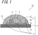
- FIG. 1 is a cross-sectional view showing one example of a light emitting apparatus having the light emitting element-mounting substrate of the present disclosure.
- the light emitting element-mounting substrate of the present disclosure can bring out high luminance and high light emission efficiency for a long period of time.
- the light emitting element-mounting substrate of the present disclosure will be described in detail referring to a drawing below.
- FIG. 1 is a cross-sectional view showing one example of the light emitting apparatus having the light emitting element-mounting substrate of the present disclosure.
- the light emitting element-mounting substrate 4 of the present disclosure has a base body 1 formed of ceramics, a metal layer 2 disposed on the base body 1, containing copper as a main component, and a glass layer 3 disposed on the base body 1 and the metal layer 2.
- the main component in the metal layer 2 refers to a component which accounts for 50% by mass or more of 100% by mass of the total of all components constituting the metal layer 2.
- the metal layer 2 has low electrical resistivity and high heat dissipation since a main component thereof is copper as described above.
- the metal layer 2 may also contain zirconium, titanium, molybdenum, tin and the like in addition to copper.
- the light emitting apparatus 10 of the present disclosure has a light emitting element 5 mounted on a metal layer 2a of the light emitting element-mounting substrate 4 having the above-described constitution.
- FIG. 1 shows an example in which the light emitting element 5 is electrically connected via a bonding wire 6 to a metal layer 2b juxtaposed to the metal layer 2a. Further, FIG. 1 shows an example in which a surface of the light emitting element-mounting substrate 4 on the side where the light emitting element 5 is mounted is covered together with the light emitting element 5 with a sealing material 7.
- This sealing material 7 may contain a fluorescent material and the like for wavelength conversion.
- the glass layer 3 of the light emitting element-mounting substrate 4 of the present disclosure exists on at least a part of the base body 1 and the metal layer 2 and has a white color tone.
- the glass layer 3 contains a compound comprising titanium and oxygen.
- the glass layer 3 of the light emitting-mounting element substrate 4 of the present disclosure has high reflection rate in the visible light range since the glass layer 3 contains a compound comprising titanium and oxygen as described above.
- the reason why high reflection rate can be provided in the visible light range is that visible light can be reflected efficiently because of high refractive index of the compound (for example, TiO 2 ) composed of titanium and oxygen.
- the compound comprising titanium and oxygen may have a form in which a compound composed of titanium and oxygen is present as a nucleus and the other compound is formed so as to cover the nucleus.
- the size of such a compound its diameter may be not less than 0.2 ⁇ m and not more than 2.0 ⁇ m.
- the glass layer 3 contains a compound comprising titanium and oxygen, a difference in thermal expansion coefficient between the glass layer 3 and the metal layer 2 containing copper as a main component is smaller, and thus, peeling when heat generated at the time of output of the light emitting element 5 is transmitted is suppressed.
- the light emitting element-mounting substrate 4 of the present disclosure can bring out high luminance and high light emission efficiency over a long period of time owing to excellent reflection rate and suppression of peeling of the glass layer 3.
- the compound contained in the glass layer 3 may be confirmed by measuring the glass layer 3 using an X-ray diffractometer (XRD) and checking the obtained result with the JCPDS card.
- XRD X-ray diffractometer
- the compound contained in the glass layer 3 can also be confirmed by using an energy dispersive X-ray spectrometer (EDS) attached to a scanning electron micrometer (SEM).
- EDS energy dispersive X-ray spectrometer
- SEM scanning electron micrometer
- the light emitting element-mounting substrate 4 is cut, and polished by a cross-section polisher (CP).
- CP cross-section polisher
- the polished cross-section is adopted as an observation surface and observed using the SEM at not less than 1000 and not more than 10000-fold magnification.
- a position visually-recognized as particle is irradiated with X-ray by the EDS attached to the SEM. If the presence of Ti and O is recognized at this position, it can be considered that a compound comprising titanium and oxygen exists.
- an area occupying ratio of the compound in the glass layer 3 may be not less than 24 area% and not more than 60 area%.
- the glass layer 3 becomes more white and the reflection rate in the visible light range can be further improved. Further, when heat generated at the time of output of the light emitting element 5 is transmitted, peeling of the glass layer 3 can be further suppressed.
- the area occupying ratio of the compound in the glass layer 3 may be calculated, for example, by the following method. First, an observation surface described above is observed using the SEM at 3000-fold magnification, and photographed. Next, on the photograph taken, a measurement area in the glass layer 3 is adjusted to 220 ⁇ m 2 , and then, binarization is conducted by coloring a position of the compound comprising titanium and oxygen, using image analysis software. Next, the area occupying ratio of the compound is determined by calculating the ratio of the colored position in the measurement area. This operation is carried out at any five positions and the average of the obtained measurement values is the area occupying ratio of the compound in the glass layer 3.
- the arithmetic mean roughness Ra on the surface 3a of the glass layer 3 may be not less than 0.18 ⁇ m and not more than 0.3 ⁇ m.
- the arithmetic mean roughness Ra on the surface 3a of the glass layer 3 may be calculated from the results of measurement of the surface 3a of the glass layer 3 according to JIS B 0601-2001 using a contact or noncontact roughness measuring instrument. Measurement of the surface 3a of the glass layer 3 is carried out at any five positions, and the average of the obtained measurement values is the arithmetic mean roughness Ra on the surface 3a of the glass layer 3.
- the glass layer 3 of the light emitting element-mounting substrate 4 of the present disclosure contains copper or zinc, and the total content of copper and zinc in the glass layer 3 may be larger in the metal layer side region than in the surface side region. Under such a constitution, the close adhesion strength between the metal layer 2 and the glass layer 3 is improved while maintaining the reflection efficiency of visible light on the surface 3a of the glass layer 3 high, and thus, peeling of the glass layer 3 can be further suppressed.
- the thickness of the glass layer 3 which is the distance from the metal layer 2 to the surface 3a is divided into three equal parts, and the region of 1/3 of the thickness of the glass layer 3 including the surface 3a is the surface side region of the glass layer 3.
- the metal layer side region of the glass layer 3 is the region of 1/3 of the thickness of the glass layer 3 including the interface between the metal layer 2 and the glass layer.
- the region sandwiched by the surface side region and the metal layer side region is referred to as the intermediate region.
- the total content of copper and zinc may gradually increase from the surface side region to the metal layer side region.
- the close adhesion strength between the metal layer 2 and the glass layer 3 is improved more, thus, peeling of the glass layer 3 can be further suppressed.
- the gradual increase means that the total content of copper and zinc satisfies the following relation: metal layer side region > intermediate region > surface side region.
- the close adhesion strength between the metal layer 2 and the glass layer 3 is further improved.
- the total content of copper and zinc in the glass layer 3 may be calculated by the following method. Further, the light emitting element-mounting substrate 4 is cut in the thickness direction and polished by the CP. Next, the polished cross-section is adopted as an observation surface and observed using the SEM at not less than 1000 and not more than 10000-fold magnification. Then, the surface side region, the intermediate region and the metal layer side region of the glass layer 3 are irradiated with X-ray and the content of copper and zinc is measured by the EDS attached to the SEM. Whether the total content of copper and zinc is larger in the metal layer side region than in the surface side region or whether the total content thereof increases gradually may be decided by confirming the total content of copper and zinc in the surface side region, the intermediate region and the metal layer side region.
- the glass layer 3 may contain zirconia. Under such a constitution, the reflection rate is further improved since the refractive index of zirconia is high and the refractive index of the compound comprising titanium and oxygen is difference from the refractive index of zirconia.
- the base body 1 constituting the light emitting element-mounting substrate 4 of the present disclosure is composed of ceramics, and aluminum oxide-based ceramics, zirconium oxide-based ceramics, composite ceramics composed of aluminum oxide and zirconium oxide, silicon nitride-based ceramics, aluminum nitride-based ceramics, silicon carbide-based ceramics, mullite-based ceramics and the like can be used as the ceramics. If the base body 1 is formed of an aluminum oxide-based ceramics, the base body 1 gets excellent mechanical strength in addition to relatively easy processability. If the base body 1 is formed of an aluminum nitride-based ceramics, the base body 1 gets more excellent heat dissipation.
- the aluminum oxide-based ceramics is ceramics containing aluminum oxide as the main component, and contains aluminum oxide in a proportion of 70% by mass or more with respect to 100% by mass of all components constituting the ceramics.
- the material of the base body 1 constituting the light emitting element-mounting substrate 4 of the present disclosure can be confirmed by the following method. First, the presence of aluminum oxide is confirmed by measuring the base body using an XRD and checking the obtained result with the JCPDS card. Next, quantitative analysis of aluminum (Al) is performed using an ICP (Inductively Coupled Plasma) emission spectrophotometer (ICP) or an X-ray fluorescence spectrometer (XRF). The content of Al measured by an ICP or XRF is converted to the content of aluminum oxide (Al 2 O 3 ) and when the converted content is 70% by mass or more, it is an aluminum oxide-based ceramics. The same applies to other ceramics.
- ICP Inductively Coupled Plasma
- XRF X-ray fluorescence spectrometer
- a through hole may be formed in the base body 1.
- a through electrode composed of an electrically conductive substance is formed in the through hole, connection to an external electrode can be attained.
- a thermal via composed of a highly thermally conductive substance is formed in the through hole, the heat dissipation of the base body 1 can be improved.
- those containing any of an R 2 O-B 2 O 3 -SiO 2 -based material (R: alkali metal element), an SiO 2 -Bi 2 O 3 -B 2 O 3 -based material and an R 2 O-SiO 2 -B 2 O 3 -Bi 2 O 3 -based material as the main component are advantageous as the glass layer 3.
- the softening points of these compounds are not lower than 700°C and not higher than 780°C.
- aluminum nitride-based ceramics and aluminum oxide-based ceramics are prepared, as the base body 1, by known molding methods and firing methods.
- barium oxide (BaO) and zirconium oxide (ZrO 2 ) may be contained for improving the reflection rate of the base body 1.
- the through hole When the through hole is formed in the base body 1, the through hole may be formed together with formation of the external form in molding. Alternatively, a hole may be formed by punching, blast or laser for a molded body having undergone processing of only the external form. Alternatively, a hole may be formed by blast or laser on a sintered body.
- the thickness of the base body 1 is, for example, not less than 0.15 mm and not more than 1.5 mm.
- the metal layer 2 can be formed by screenprinting a pattern of wiring and electrodes on the base body 1 using a known metal paste containing copper as the main component, and then, firing it under a nitrogen atmosphere.
- the thickness of the metal layer 2 is, for example, not less than 10 ⁇ m and not more than 18 ⁇ m.
- printing, drying and thermal treatment may be repeated, or steps until printing and drying may be conducted several times before collective thermal treatment.
- a glass paste is prepared for forming the glass layer 3.
- glass powder containing any of an R 2 O-B 2 O 3 -SiO 2 -based material (R: alkali metal element), an SiO 2 -Bi 2 O 3 -B 2 O 3 -based material and an R 2 O-SiO 2 -B 2 O 3 -Bi 2 O 3 -based material as the main component is prepared.
- the average particle size of the glass powder is, for example, not less than 2 ⁇ m and not more than 4 ⁇ m.
- titanium oxide powder having an average particle size of not less than 0.1 ⁇ m and not more than 2.0 ⁇ m is prepared.
- the titanium oxide powder is weighed so that the amount thereof is not less than 15 parts by mass and not more than 25 parts by mass with respect to 100 parts by mass of the glass powder.
- an organic vehicle is prepared.
- the organic vehicle is obtained by dissolving an organic binder in an organic solvent, and for example, the mass ratio of the organic binder to the organic solvent is 1 : 2 to 6.
- One or more substances selected from, for example, acryls such as polybutyl methacrylate and polymethyl methacrylate, celluloses such as nitro cellulose, ethyl cellulose, cellulose acetate and butyl cellulose, polyethers such as polyoxymethylene, and polyvinyls such as polybutadiene and polyisoprene can be mixed and used as the organic binder.
- One or more substances selected from, for example, carbitol, carbitol acetate, terpineol, meta-cresol, dimethylimidazole, dimethylimidazolidinone, dimethyl formamide, diacetone alcohol, triethylene glycol, p-xylene, ethyl lactate and isophorone can be mixed and used as the organic solvent.
- the glass powder, the titanium oxide powder and the organic vehicle are weighed in desired amounts and mixed, to prepare a glass paste.
- the amount of mixed powder of the glass powder and the titanium oxide powder is not less than 60 parts by mass and not more than 80 parts by mass with respect to 100 parts by mass of the glass paste and the rest is the organic vehicle, for example.
- zirconia powder having an average particle size of not less than 0.1 ⁇ m and not more than 2 ⁇ m is prepared and weighed so that its amount is not less than 0.1 part by mass and not more than 5 parts by mass with respect to 100 parts by mass of the glass powder, and added to the above-described glass paste.
- the obtained glass paste is printed so as to cover desired regions on the base body 1 and the metal layer 2, and dried and defatted at temperatures of not lower than 80°C and not higher than 140°C.
- the glass layer 3 contains copper or zinc and the total content of copper and zinc in the glass layer 3 is larger in the metal layer side region than in the surface side region
- a glass paste is prepared as described below and printed so as to cover desired regions.
- copper powder and zinc powder are added, and 3 kinds of glass pastes having different total contents of copper and zinc are prepared.
- a first glass paste forming the metal layer side region, a second glass paste forming the intermediate region and a third glass paste forming the surface side region, in the glass layer 3, are prepared.
- the first glass paste is prepared so that the total content of copper and zinc is larger than in the third glass paste. It may be recommendable that the first glass paste is printed so as to cover desired regions on the base body 1 and the metal layer 2, the second glass paste is printed on the first glass paste, and the third glass paste is printed on the second glass paste.
- each glass paste is prepared so that the total content of copper and zinc satisfies the following relation: first glass paste > second glass paste > third glass paste, the total content of copper and zinc gradually increases from the surface side region to the metal layer side region in the glass layer 3.
- the printed glass paste is thermally treated by keeping it under a nitrogen atmosphere at a maximum temperature of not lower than 800°C and not higher than 950°C for not shorter than 2 minutes and not longer than 15 minutes.
- a maximum temperature in the thermal treatment is higher or when the time of the thermal treatment is longer, a larger amount of the compound comprising titanium and oxygen can be deposited, however, when the maximum temperature is higher than 950°C or when the keeping time of the maximum temperature is 15 minutes or longer, carbon that could not be removed during degreasing bursts, to form pin holes inside the glass layer 3, thereby hindering whitening.
- the thickness of the glass layer 3 is, for example, not less than 10 ⁇ m and not more than 20 ⁇ m.
- the surface of the glass layer 3 may be ground using a surface grinding machine.
- the surface of the metal layer 2 not covered with the glass layer 3 may be partially plated.
- the plating may be publicly known plating and examples thereof include gold plating, silver plating, nickel-gold plating and nickel-palladium-gold plating.
- the base body 1 having split grooves formed thereon is used and the metal layer 2 and the glass layer 3 are formed by the above-described method, and then, the base body 1 is split, it is possible to efficiently fabricate a lot of light emitting element-mounting substrates 4.
- the production method of the light emitting element-mounting substrate 4 of the present disclosure is not limited to the above-described production method.
- the light emitting apparatus 10 of the present disclosure can be obtained, for example, by mounting the light emitting element 5 on the metal layer 2a of the light emitting element-mounting substrate 4 of the present disclosure.
- the light emitting apparatus 10 of the present disclosure fabricated as described above can bring out high luminance and high light emission efficiency over a long period of time.
- Samples of different constitutions were fabricated and subjected to tests of reflection rate and heat cycle.
- aluminum oxide-based ceramics having a thickness of 1.0 mm was prepared as a base body.
- a metal paste containing copper as the main component was screen-printed on the base body, and then fired under a nitrogen atmosphere, to form a metal layer having a thickness of 14 ⁇ m.
- R 2 O-B 2 O 3 -SiO 2 -based glass powder (R: alkali metal element) having an average particle size of 3 ⁇ m was prepared. Further, titanium oxide powder having an average particle size of 1 ⁇ m was prepared. The titanium oxide powder was weighed so as to give amounts shown in Table 1 with respect to 100 parts by mass of the glass powder.
- an organic vehicle was prepared, and desired amounts of the glass powder, the titanium oxide powder and the organic vehicle were weighed and mixed, to prepare a glass paste.
- the total of the glass powder and the titanium oxide powder was 70 parts by mass and the rest was the organic vehicle.
- the obtained glass paste was printed so as to cover desired regions on the base body and the metal layer, and dried and degreased at a temperature of 120°C.
- the printed glass paste was thermally treated by keeping under a nitrogen atmosphere at the maximum temperature shown in Table 1 for 5 minutes, to obtain sample Nos. 1 to 11 in which the thickness of the glass layer was 16 ⁇ m and the longitudinal size ⁇ the lateral size were 17 mm ⁇ 17 mm. For each sample, multiple copies were fabricated for conducting the heat cycle test.
- the glass layer of each sample was measured using a spectrophotometer (CM-3700A manufactured by Minolta) under conditions of a reference light source of D65, a wavelength range of 360 to 740 nm, a field of view of 10° and an illumination size of 3 ⁇ 5 mm, and reflection rate at 500 nm was measured from the measurement results.
- CM-3700A manufactured by Minolta
- the heat cycle test was conducted by the following method. First, 16 copies of each sample were prepared, and a cycle in which the environmental temperature of each sample was lowered from room temperature (25°C) to -40°C and kept for 30 minutes and raised to 125°C and kept for 30 minutes, and then lowered to room temperature, was regarded as one cycle and repeated, using a cold and heat impact test element. During 2500 cycles to 4500 cycles, each one of the each sample was taken out every 100 cycles, and a polyester film was pasted onto the surface of the glass layer and a peel test was conducted by pulling the film upward. The number of cycles when peeling of the glass layer from the metal layer was confirmed was examined by this peel test. The results are shown in Table 1. [Table 1] Sample No.
- Titanium oxide Part by mass
- Thermal treatment temperature °C
- Area occupying ratio of compound (Area%)
- Reflection rate at 500 nm %
- Number of cycles 1 15 750 0 39.8 2800 2 15 775 8 43.1 3500 3 15 800 15 45.6 3600 4 15 850 24 48.8 4000 5 15 900 42 50.8 4000 6 15 950 44 52.5 4000 7 15 1000 - - - 8 25 850 33 49.2 4000 9 25 900 58 61.2 4000 10 25 950 60 62.4 4000 11 25 1000 - - -
- the reflection rate at 500 nm was 40% or more and the number of cycles was 3500 or more.
- the reflection rate at 500 nm was 48.8% or more and the number of cycles was 4000, that is, it was found that the area occupying ratio of the compound in the glass layer is preferably not less than 24 area% and not more than 60 area%.
- samples having different arithmetic mean roughnesses Ra on the surface of the glass layer were fabricated, and the reflection rate was measured. Fabrication of the sample was conducted in the same manner as for the sample No. 6 in Example 1, and for the sample Nos. 13 to 16, the surface of the glass layer was ground so that the arithmetic mean roughness Ra varied using a surface grinding machine.
- the sample No. 12 is the same as the sample No. 6 in Example 1.
- the content of copper and zinc in the glass layer was calculated by the following method. First, each sample was cut in the thickness direction and polished by the CP. Next, the polished cross-section was adopted as an observation surface and observed at 3000-fold magnification using the SEM. The surface side region, the intermediate region and the metal layer side region of the glass layer of each sample were irradiated with X-ray by the EDS attached to the SEM, and the content of copper and zinc was measured.
- the area occupying ratio of the compound was determined by the same manner as in Example 1. As a result, the area occupying ratio of the compound was 44 area% for the glass layers of all the samples.
- the reflection rate at 500 nm was 50% or more and the number of cycles was 4100 or more. It was found from this result that when the content of copper and zinc in the glass layer is larger in the metal layer side region than in the surface side region, the close adhesion strength between the metal layer and the glass layer is further improved while maintaining the reflection efficiency of visible light on the surface of the glass layer high.
- the reflection rate at 500 nm of the sample was 51% or more and the number of cycles was 4300 or more. It was found from this result that it is more preferable that the content of copper and zinc in the glass layer increases gradually from the surface side region to the metal layer side region.
- sample No. 27 was the same as the sample No. 14 in Example 2
- sample No. 28 was fabricated in the same manner as for the sample No. 14 in Example 2 except that the zirconia powder was added in an amount of 2 parts by mass and the amount of the glass powder was reduced correspondingly.
Landscapes
- Chemical & Material Sciences (AREA)
- Engineering & Computer Science (AREA)
- Materials Engineering (AREA)
- Organic Chemistry (AREA)
- Chemical Kinetics & Catalysis (AREA)
- Geochemistry & Mineralogy (AREA)
- General Chemical & Material Sciences (AREA)
- Life Sciences & Earth Sciences (AREA)
- Ceramic Engineering (AREA)
- Dispersion Chemistry (AREA)
- Manufacturing & Machinery (AREA)
- Structural Engineering (AREA)
- Led Device Packages (AREA)
- Non-Metallic Protective Coatings For Printed Circuits (AREA)
Abstract
Description
- The present disclosure relates to a light emitting element-mounting substrate and a light emitting apparatus.
- As a light emitting element with low electric power consumption, light emitting diodes (LED) are attracting attention. For mounting such LED, an insulating substrate is used and a metal layer acting as a circuit (wiring) is provided on this substrate.
- Under such a constitution, the heat at the output of LED exerts an influence on performance and reliability of LED, thus, a resin is used as the substrate material for low output LED and ceramics is used as the substrate material for medium or above output LED.
- In a light emitting apparatus having a light emitting element on a metal layer of a substrate having the above-described constitution, the substrate and the metal layer disposed on the substrate are covered with a white color tone resin (hereinafter, described as white resin) for the purpose of improvement of light emission efficiency, protection of the metal layer and the like
- Patent Literature 1: Japanese Unexamined Patent Publication
JP-A 2009-129801 - A light emitting element-mounting substrate of the present disclosure comprises a base body formed of ceramics; a metal layer disposed on the base body, and containing copper as a main component; and a glass layer disposed on the metal layer, having a white color tone, and containing a compound comprising titanium and oxygen.
-
FIG. 1 is a cross-sectional view showing one example of a light emitting apparatus having the light emitting element-mounting substrate of the present disclosure. - With recent increase in luminance, a lot of heat is transferred to a metal layer. Since the metal layer has high thermal conductivity, a large amount of heat is transferred also to a white resin. When a lot of heat is transferred to the white resin as described above, close adhesion between the metal layer and the white resin tends to lower. If the white resin is peeled off from the metal layer, light emission efficiency lowers and the metal layer cannot be protected, thus, high light emission efficiency of LED cannot be brought out for a long period of time.
- The light emitting element-mounting substrate of the present disclosure can bring out high luminance and high light emission efficiency for a long period of time. The light emitting element-mounting substrate of the present disclosure will be described in detail referring to a drawing below.
-
FIG. 1 is a cross-sectional view showing one example of the light emitting apparatus having the light emitting element-mounting substrate of the present disclosure. - As shown in
FIG. 1 , the light emitting element-mounting substrate 4 of the present disclosure has abase body 1 formed of ceramics, ametal layer 2 disposed on thebase body 1, containing copper as a main component, and aglass layer 3 disposed on thebase body 1 and themetal layer 2. - Here, the main component in the
metal layer 2 refers to a component which accounts for 50% by mass or more of 100% by mass of the total of all components constituting themetal layer 2. Themetal layer 2 has low electrical resistivity and high heat dissipation since a main component thereof is copper as described above. Themetal layer 2 may also contain zirconium, titanium, molybdenum, tin and the like in addition to copper. - The
light emitting apparatus 10 of the present disclosure has alight emitting element 5 mounted on ametal layer 2a of the light emitting element-mounting substrate 4 having the above-described constitution.FIG. 1 shows an example in which thelight emitting element 5 is electrically connected via abonding wire 6 to ametal layer 2b juxtaposed to themetal layer 2a. Further,FIG. 1 shows an example in which a surface of the light emitting element-mounting substrate 4 on the side where thelight emitting element 5 is mounted is covered together with thelight emitting element 5 with asealing material 7. This sealingmaterial 7 may contain a fluorescent material and the like for wavelength conversion. - The
glass layer 3 of the light emitting element-mounting substrate 4 of the present disclosure exists on at least a part of thebase body 1 and themetal layer 2 and has a white color tone. Theglass layer 3 contains a compound comprising titanium and oxygen. Theglass layer 3 of the light emitting-mounting element substrate 4 of the present disclosure has high reflection rate in the visible light range since theglass layer 3 contains a compound comprising titanium and oxygen as described above. - The reason why high reflection rate can be provided in the visible light range is that visible light can be reflected efficiently because of high refractive index of the compound (for example, TiO2) composed of titanium and oxygen. The compound comprising titanium and oxygen may have a form in which a compound composed of titanium and oxygen is present as a nucleus and the other compound is formed so as to cover the nucleus. Regarding the size of such a compound, its diameter may be not less than 0.2 µm and not more than 2.0 µm.
- Since the
glass layer 3 contains a compound comprising titanium and oxygen, a difference in thermal expansion coefficient between theglass layer 3 and themetal layer 2 containing copper as a main component is smaller, and thus, peeling when heat generated at the time of output of thelight emitting element 5 is transmitted is suppressed. Hence, the light emitting element-mounting substrate 4 of the present disclosure can bring out high luminance and high light emission efficiency over a long period of time owing to excellent reflection rate and suppression of peeling of theglass layer 3. - The compound contained in the
glass layer 3 may be confirmed by measuring theglass layer 3 using an X-ray diffractometer (XRD) and checking the obtained result with the JCPDS card. - Alternatively, the compound contained in the
glass layer 3 can also be confirmed by using an energy dispersive X-ray spectrometer (EDS) attached to a scanning electron micrometer (SEM). First, the light emitting element-mounting substrate 4 is cut, and polished by a cross-section polisher (CP). Next, the polished cross-section is adopted as an observation surface and observed using the SEM at not less than 1000 and not more than 10000-fold magnification. Next, a position visually-recognized as particle is irradiated with X-ray by the EDS attached to the SEM. If the presence of Ti and O is recognized at this position, it can be considered that a compound comprising titanium and oxygen exists. - Alternatively, if a region where Ti exists and a region where O exists overlap in element mapping at a position visually recognized as particle using an electron probe microanalyzer (EPMA), it can be considered that a compound comprising titanium and oxygen exists.
- In the light emitting element-
mounting substrate 4 of the present disclosure, an area occupying ratio of the compound in theglass layer 3 may be not less than 24 area% and not more than 60 area%. When such a constitution is satisfied, theglass layer 3 becomes more white and the reflection rate in the visible light range can be further improved. Further, when heat generated at the time of output of thelight emitting element 5 is transmitted, peeling of theglass layer 3 can be further suppressed. - The area occupying ratio of the compound in the
glass layer 3 may be calculated, for example, by the following method. First, an observation surface described above is observed using the SEM at 3000-fold magnification, and photographed. Next, on the photograph taken, a measurement area in theglass layer 3 is adjusted to 220 µm2, and then, binarization is conducted by coloring a position of the compound comprising titanium and oxygen, using image analysis software. Next, the area occupying ratio of the compound is determined by calculating the ratio of the colored position in the measurement area. This operation is carried out at any five positions and the average of the obtained measurement values is the area occupying ratio of the compound in theglass layer 3. - In the light emitting element-
mounting substrate 4 of the present disclosure, the arithmetic mean roughness Ra on thesurface 3a of theglass layer 3 may be not less than 0.18 µm and not more than 0.3 µm. When such a constitution is satisfied, since the reflection rate of visible light on thesurface 3a of theglass layer 3 is enhanced, the reflection rate in the visible light range is further improved. - The arithmetic mean roughness Ra on the
surface 3a of theglass layer 3 may be calculated from the results of measurement of thesurface 3a of theglass layer 3 according to JIS B 0601-2001 using a contact or noncontact roughness measuring instrument. Measurement of thesurface 3a of theglass layer 3 is carried out at any five positions, and the average of the obtained measurement values is the arithmetic mean roughness Ra on thesurface 3a of theglass layer 3. - The
glass layer 3 of the light emitting element-mounting substrate 4 of the present disclosure contains copper or zinc, and the total content of copper and zinc in theglass layer 3 may be larger in the metal layer side region than in the surface side region. Under such a constitution, the close adhesion strength between themetal layer 2 and theglass layer 3 is improved while maintaining the reflection efficiency of visible light on thesurface 3a of theglass layer 3 high, and thus, peeling of theglass layer 3 can be further suppressed. - For the
glass layer 3 appearing in the cross-section obtained by cutting the light emitting element-mounting substrate 4 in the thickness direction, the thickness of theglass layer 3 which is the distance from themetal layer 2 to thesurface 3a is divided into three equal parts, and the region of 1/3 of the thickness of theglass layer 3 including thesurface 3a is the surface side region of theglass layer 3. The metal layer side region of theglass layer 3 is the region of 1/3 of the thickness of theglass layer 3 including the interface between themetal layer 2 and the glass layer. In theglass layer 3, the region sandwiched by the surface side region and the metal layer side region is referred to as the intermediate region. - In the
glass layer 3 of the light emitting element-mounting substrate 4 of the present disclosure, the total content of copper and zinc may gradually increase from the surface side region to the metal layer side region. Under such a constitution, the close adhesion strength between themetal layer 2 and theglass layer 3 is improved more, thus, peeling of theglass layer 3 can be further suppressed. The gradual increase means that the total content of copper and zinc satisfies the following relation: metal layer side region > intermediate region > surface side region. - When the total content of copper and zinc in the metal layer side region of the
glass layer 3 is 3% by mass or more, the close adhesion strength between themetal layer 2 and theglass layer 3 is further improved. - The total content of copper and zinc in the
glass layer 3 may be calculated by the following method. Further, the light emitting element-mountingsubstrate 4 is cut in the thickness direction and polished by the CP. Next, the polished cross-section is adopted as an observation surface and observed using the SEM at not less than 1000 and not more than 10000-fold magnification. Then, the surface side region, the intermediate region and the metal layer side region of theglass layer 3 are irradiated with X-ray and the content of copper and zinc is measured by the EDS attached to the SEM. Whether the total content of copper and zinc is larger in the metal layer side region than in the surface side region or whether the total content thereof increases gradually may be decided by confirming the total content of copper and zinc in the surface side region, the intermediate region and the metal layer side region. - In the light emitting element-mounting
substrate 4 of the present disclosure, theglass layer 3 may contain zirconia. Under such a constitution, the reflection rate is further improved since the refractive index of zirconia is high and the refractive index of the compound comprising titanium and oxygen is difference from the refractive index of zirconia. - The
base body 1 constituting the light emitting element-mountingsubstrate 4 of the present disclosure is composed of ceramics, and aluminum oxide-based ceramics, zirconium oxide-based ceramics, composite ceramics composed of aluminum oxide and zirconium oxide, silicon nitride-based ceramics, aluminum nitride-based ceramics, silicon carbide-based ceramics, mullite-based ceramics and the like can be used as the ceramics. If thebase body 1 is formed of an aluminum oxide-based ceramics, thebase body 1 gets excellent mechanical strength in addition to relatively easy processability. If thebase body 1 is formed of an aluminum nitride-based ceramics, thebase body 1 gets more excellent heat dissipation. - For example, the aluminum oxide-based ceramics is ceramics containing aluminum oxide as the main component, and contains aluminum oxide in a proportion of 70% by mass or more with respect to 100% by mass of all components constituting the ceramics. The material of the
base body 1 constituting the light emitting element-mountingsubstrate 4 of the present disclosure can be confirmed by the following method. First, the presence of aluminum oxide is confirmed by measuring the base body using an XRD and checking the obtained result with the JCPDS card. Next, quantitative analysis of aluminum (Al) is performed using an ICP (Inductively Coupled Plasma) emission spectrophotometer (ICP) or an X-ray fluorescence spectrometer (XRF). The content of Al measured by an ICP or XRF is converted to the content of aluminum oxide (Al2O3) and when the converted content is 70% by mass or more, it is an aluminum oxide-based ceramics. The same applies to other ceramics. - A through hole may be formed in the
base body 1. When the through hole is formed in thebase body 1 and a through electrode composed of an electrically conductive substance is formed in the through hole, connection to an external electrode can be attained. When a thermal via composed of a highly thermally conductive substance is formed in the through hole, the heat dissipation of thebase body 1 can be improved. - Next, those containing any of an R2O-B2O3-SiO2-based material (R: alkali metal element), an SiO2-Bi2O3-B2O3-based material and an R2O-SiO2-B2O3-Bi2O3-based material as the main component are advantageous as the
glass layer 3. The softening points of these compounds are not lower than 700°C and not higher than 780°C. - One example of the production method of the light emitting element-mounting
substrate 4 of the present disclosure will be illustrated below. First, for example, aluminum nitride-based ceramics and aluminum oxide-based ceramics are prepared, as thebase body 1, by known molding methods and firing methods. In fabrication of the aluminum oxide-based ceramics, barium oxide (BaO) and zirconium oxide (ZrO2) may be contained for improving the reflection rate of thebase body 1. - When the through hole is formed in the
base body 1, the through hole may be formed together with formation of the external form in molding. Alternatively, a hole may be formed by punching, blast or laser for a molded body having undergone processing of only the external form. Alternatively, a hole may be formed by blast or laser on a sintered body. The thickness of thebase body 1 is, for example, not less than 0.15 mm and not more than 1.5 mm. - Next, the
metal layer 2 can be formed by screenprinting a pattern of wiring and electrodes on thebase body 1 using a known metal paste containing copper as the main component, and then, firing it under a nitrogen atmosphere. The thickness of themetal layer 2 is, for example, not less than 10 µm and not more than 18 µm. For controlling the thickness of themetal layer 2 at desirable level, printing, drying and thermal treatment may be repeated, or steps until printing and drying may be conducted several times before collective thermal treatment. - Next, a glass paste is prepared for forming the
glass layer 3. First, glass powder containing any of an R2O-B2O3-SiO2-based material (R: alkali metal element), an SiO2-Bi2O3-B2O3-based material and an R2O-SiO2-B2O3-Bi2O3-based material as the main component is prepared. The average particle size of the glass powder is, for example, not less than 2 µm and not more than 4 µm. - Further, titanium oxide powder having an average particle size of not less than 0.1 µm and not more than 2.0 µm is prepared. The titanium oxide powder is weighed so that the amount thereof is not less than 15 parts by mass and not more than 25 parts by mass with respect to 100 parts by mass of the glass powder.
- Next, an organic vehicle is prepared. The organic vehicle is obtained by dissolving an organic binder in an organic solvent, and for example, the mass ratio of the organic binder to the organic solvent is 1 : 2 to 6. One or more substances selected from, for example, acryls such as polybutyl methacrylate and polymethyl methacrylate, celluloses such as nitro cellulose, ethyl cellulose, cellulose acetate and butyl cellulose, polyethers such as polyoxymethylene, and polyvinyls such as polybutadiene and polyisoprene can be mixed and used as the organic binder.
- One or more substances selected from, for example, carbitol, carbitol acetate, terpineol, meta-cresol, dimethylimidazole, dimethylimidazolidinone, dimethyl formamide, diacetone alcohol, triethylene glycol, p-xylene, ethyl lactate and isophorone can be mixed and used as the organic solvent.
- The glass powder, the titanium oxide powder and the organic vehicle are weighed in desired amounts and mixed, to prepare a glass paste. Regarding the blending amounts, it may be recommendable that the amount of mixed powder of the glass powder and the titanium oxide powder is not less than 60 parts by mass and not more than 80 parts by mass with respect to 100 parts by mass of the glass paste and the rest is the organic vehicle, for example.
- When the
glass layer 3 contains zirconia, it may be recommendable that zirconia powder having an average particle size of not less than 0.1 µm and not more than 2 µm is prepared and weighed so that its amount is not less than 0.1 part by mass and not more than 5 parts by mass with respect to 100 parts by mass of the glass powder, and added to the above-described glass paste. - The obtained glass paste is printed so as to cover desired regions on the
base body 1 and themetal layer 2, and dried and defatted at temperatures of not lower than 80°C and not higher than 140°C. - In the case wherein the
glass layer 3 contains copper or zinc and the total content of copper and zinc in theglass layer 3 is larger in the metal layer side region than in the surface side region, it may be recommendable that a glass paste is prepared as described below and printed so as to cover desired regions. First, in preparation of the above-described glass paste, copper powder and zinc powder are added, and 3 kinds of glass pastes having different total contents of copper and zinc are prepared. Specifically, a first glass paste forming the metal layer side region, a second glass paste forming the intermediate region and a third glass paste forming the surface side region, in theglass layer 3, are prepared. The first glass paste is prepared so that the total content of copper and zinc is larger than in the third glass paste. It may be recommendable that the first glass paste is printed so as to cover desired regions on thebase body 1 and themetal layer 2, the second glass paste is printed on the first glass paste, and the third glass paste is printed on the second glass paste. - If each glass paste is prepared so that the total content of copper and zinc satisfies the following relation: first glass paste > second glass paste > third glass paste, the total content of copper and zinc gradually increases from the surface side region to the metal layer side region in the
glass layer 3. - Next, the printed glass paste is thermally treated by keeping it under a nitrogen atmosphere at a maximum temperature of not lower than 800°C and not higher than 950°C for not shorter than 2 minutes and not longer than 15 minutes. When the maximum temperature in the thermal treatment is higher or when the time of the thermal treatment is longer, a larger amount of the compound comprising titanium and oxygen can be deposited, however, when the maximum temperature is higher than 950°C or when the keeping time of the maximum temperature is 15 minutes or longer, carbon that could not be removed during degreasing bursts, to form pin holes inside the
glass layer 3, thereby hindering whitening. - The thickness of the
glass layer 3 is, for example, not less than 10 µm and not more than 20 µm. Through the above-described process, the light emitting element-mountingsubstrate 4 of the present disclosure can be obtained. - For obtaining the arithmetic mean roughness Ra on the surface of the
glass layer 3, the surface of theglass layer 3 may be ground using a surface grinding machine. - Further, the surface of the
metal layer 2 not covered with theglass layer 3 may be partially plated. By conducting a plating treatment as described above, it becomes easy to perform a close adhesion treatment of thelight emitting element 5 and thebonding wire 6, and corrosion of themetal layer 2 due to oxidation can be suppressed. The plating may be publicly known plating and examples thereof include gold plating, silver plating, nickel-gold plating and nickel-palladium-gold plating. - In fabrication of the light emitting element-mounting
substrate 4 of the present disclosure, if thebase body 1 having split grooves formed thereon is used and themetal layer 2 and theglass layer 3 are formed by the above-described method, and then, thebase body 1 is split, it is possible to efficiently fabricate a lot of light emitting element-mountingsubstrates 4. The production method of the light emitting element-mountingsubstrate 4 of the present disclosure is not limited to the above-described production method. - Next, the
light emitting apparatus 10 of the present disclosure can be obtained, for example, by mounting thelight emitting element 5 on themetal layer 2a of the light emitting element-mountingsubstrate 4 of the present disclosure. Thelight emitting apparatus 10 of the present disclosure fabricated as described above can bring out high luminance and high light emission efficiency over a long period of time. - Examples of the present disclosure will be illustrated specifically below, but the present disclosure is not limited to the following examples.
- Samples of different constitutions were fabricated and subjected to tests of reflection rate and heat cycle. First, aluminum oxide-based ceramics having a thickness of 1.0 mm was prepared as a base body. Next, a metal paste containing copper as the main component was screen-printed on the base body, and then fired under a nitrogen atmosphere, to form a metal layer having a thickness of 14 µm.
- Next, R2O-B2O3-SiO2-based glass powder (R: alkali metal element) having an average particle size of 3 µm was prepared. Further, titanium oxide powder having an average particle size of 1 µm was prepared. The titanium oxide powder was weighed so as to give amounts shown in Table 1 with respect to 100 parts by mass of the glass powder.
- Next, an organic vehicle was prepared, and desired amounts of the glass powder, the titanium oxide powder and the organic vehicle were weighed and mixed, to prepare a glass paste. Regarding the blending amount, the total of the glass powder and the titanium oxide powder was 70 parts by mass and the rest was the organic vehicle.
- The obtained glass paste was printed so as to cover desired regions on the base body and the metal layer, and dried and degreased at a temperature of 120°C.
- Next, the printed glass paste was thermally treated by keeping under a nitrogen atmosphere at the maximum temperature shown in Table 1 for 5 minutes, to obtain sample Nos. 1 to 11 in which the thickness of the glass layer was 16 µm and the longitudinal size × the lateral size were 17 mm × 17 mm. For each sample, multiple copies were fabricated for conducting the heat cycle test.
- Each sample was observed at 3000-fold magnification using the SEM and photographed and the measurement area in the glass layer was adjusted to 220 µm2, then, binarization was conducted by coloring a position of the compound comprising titanium and oxygen, using image analysis software. Next, the area occupying ratio of the compound was determined by calculating the ratio of the colored position in the measurement area. This operation was carried out at any five positions, and the average of the obtained measurement values was the area occupying ratio of the compound.
- The glass layer of each sample was measured using a spectrophotometer (CM-3700A manufactured by Minolta) under conditions of a reference light source of D65, a wavelength range of 360 to 740 nm, a field of view of 10° and an illumination size of 3 × 5 mm, and reflection rate at 500 nm was measured from the measurement results.
- The heat cycle test was conducted by the following method. First, 16 copies of each sample were prepared, and a cycle in which the environmental temperature of each sample was lowered from room temperature (25°C) to -40°C and kept for 30 minutes and raised to 125°C and kept for 30 minutes, and then lowered to room temperature, was regarded as one cycle and repeated, using a cold and heat impact test element. During 2500 cycles to 4500 cycles, each one of the each sample was taken out every 100 cycles, and a polyester film was pasted onto the surface of the glass layer and a peel test was conducted by pulling the film upward. The number of cycles when peeling of the glass layer from the metal layer was confirmed was examined by this peel test. The results are shown in Table 1.
[Table 1] Sample No. Titanium oxide (Part by mass) Thermal treatment temperature (°C) Area occupying ratio of compound (Area%) Reflection rate at 500 nm (%) Number of cycles (Number) 1 15 750 0 39.8 2800 2 15 775 8 43.1 3500 3 15 800 15 45.6 3600 4 15 850 24 48.8 4000 5 15 900 42 50.8 4000 6 15 950 44 52.5 4000 7 15 1000 - - - 
8 25 850 33 49.2 4000 9 25 900 58 61.2 4000 10 25 950 60 62.4 4000 11 25 1000 - - - 
- As shown in Table 1, for the sample No. 1, the presence of the compound comprising titanium and oxygen was not confirmed, the reflection rate at 500 nm was 40% or less, and the number of cycles was 2800. For the sample Nos. 7 and 11, the heat cycle test was not conducted since pin holes were generated in the glass layer and the metal layer swelled after the thermal treatment.
- In contrast, for the sample Nos. 2 to 6 and the sample Nos. 8 to 10, the reflection rate at 500 nm was 40% or more and the number of cycles was 3500 or more.
- It was found from this result that when the glass layer contains the compound comprising titanium and oxygen, a light emitting element-mounting substrate which can bring out high luminance and high light emission efficiency for a long period of times is obtained.
- For the sample Nos. 4 to 6 and the sample Nos. 8 to 10, the reflection rate at 500 nm was 48.8% or more and the number of cycles was 4000, that is, it was found that the area occupying ratio of the compound in the glass layer is preferably not less than 24 area% and not more than 60 area%.
- Next, samples having different arithmetic mean roughnesses Ra on the surface of the glass layer were fabricated, and the reflection rate was measured. Fabrication of the sample was conducted in the same manner as for the sample No. 6 in Example 1, and for the sample Nos. 13 to 16, the surface of the glass layer was ground so that the arithmetic mean roughness Ra varied using a surface grinding machine. In this example, the sample No. 12 is the same as the sample No. 6 in Example 1.
- The reflection rate was measured in the same manner as in Example 1. The results are shown in Table 2.
[Table 2] Sample No. Ra (µm) Reflection rate at 500 nm (%) 
12 0.10 52.5 13 0.18 53.4 14 0.24 54.5 15 0.30 53.0 16 0.40 52.0 - As shown in Table 2, an improvement in the reflection rate was observed in the sample Nos. 13 to 15. It was found from this result that the reflection rate is improved when the arithmetic mean roughness Ra on the surface of the glass layer is not less than 0.18 µm and not more than 0.3 µm.
- Next, samples having different contents of copper and zinc in the glass layer were fabricated, and subjected to the heat cycle test and measurement of the reflection rate. In fabrication of the sample, copper powder and zinc powder were added in fabricating the glass paste in the same manner as in Example 1 so that the area occupying ratio of the compound of No. 6 in Example 1 was obtained and contents of copper and zinc shown in Table 3 were obtained, thus, 3 kinds of glass pastes having different contents of copper and zinc were fabricated.
Specifically, a first glass paste forming the metal layer side region, a second glass paste forming the intermediate region and a third glass paste forming the surface side region, in theglass layer 3, were fabricated. The first glass paste was printed so as to cover desired regions on the base body and the metal layer, the second glass paste was printed on the first glass paste, and the third glass paste was printed on the second glass paste. The other conditions were the same as for the sample No. 6 in Example 1. - Next, the content of copper and zinc in the glass layer was calculated by the following method. First, each sample was cut in the thickness direction and polished by the CP. Next, the polished cross-section was adopted as an observation surface and observed at 3000-fold magnification using the SEM. The surface side region, the intermediate region and the metal layer side region of the glass layer of each sample were irradiated with X-ray by the EDS attached to the SEM, and the content of copper and zinc was measured.
- The area occupying ratio of the compound was determined by the same manner as in Example 1. As a result, the area occupying ratio of the compound was 44 area% for the glass layers of all the samples.
- The heat cycle test and measurement of the reflection rate were conducted in the same manner as in Example 1. The results are shown in Table 3.
[Table 3] Sample No. Glass layer Reflection rate at 500 nm (%) Number of cycles (number) Metal layer side region Intermediate region Surface side region Copper (% by mass) Zinc (% by mass) Total amount (% by mass) Copper (% by mass) Zinc (% by mass) Total amount (% by mass) Copper (% by mass) Zinc (% by mass) Total amount (% by mass) 17 2.1 0.0 2.1 0.0 0.0 0.0 0.0 0.0 0.0 52.5 4100 18 3.0 0.0 3.0 0.0 0.0 0.0 0.0 0.0 0.0 52.4 4200 19 6.3 0.0 6.3 4.5 0.0 4.5 0.0 0.0 0.0 52.1 4400 20 6.3 0.0 6.3 0.0 0.0 0.0 9.0 0.0 9.0 49.5 4400 21 8.4 0.0 8.4 7.1 0.0 7.1 6.6 0.0 6.6 51.5 4500 22 9.1 0.0 9.1 7.9 0.0 7.9 7.6 0.0 7.6 51.3 4500 23 9.1 0.0 9.1 10.1 0.0 10.1 7.5 0.0 7.5 50.3 4500 24 2.8 0.1 2.9 0.0 0.0 0.0 0.0 0.0 0.0 52.3 4100 25 4.4 3.0 7.4 2.8 1.2 4.0 1.1 0.0 1.1 51.8 4400 26 7.9 5.4 13.3 6.4 3.0 9.4 5.8 1.0 6.8 51.0 4500□ - As shown in Table 3, for the sample Nos. 17 to 19 and 21 to 26, the reflection rate at 500 nm was 50% or more and the number of cycles was 4100 or more. It was found from this result that when the content of copper and zinc in the glass layer is larger in the metal layer side region than in the surface side region, the close adhesion strength between the metal layer and the glass layer is further improved while maintaining the reflection efficiency of visible light on the surface of the glass layer high.
- For the sample Nos. 19, 21, 22, 25 and 26, the reflection rate at 500 nm of the sample was 51% or more and the number of cycles was 4300 or more. It was found from this result that it is more preferable that the content of copper and zinc in the glass layer increases gradually from the surface side region to the metal layer side region.
- Samples in which zirconia is present or absent in the glass layer were fabricated, and the reflection rate was measured. In fabrication of the sample, the sample No. 27 was the same as the sample No. 14 in Example 2, and the sample No. 28 was fabricated in the same manner as for the sample No. 14 in Example 2 except that the zirconia powder was added in an amount of 2 parts by mass and the amount of the glass powder was reduced correspondingly.
- The reflection rate was measured by the same manner as in Example 1. The results are shown in Table 4.
[Table 4] Sample No. Presence or absence of zirconia Reflection rate at 500 nm (%) 27 Absence 54.5 28 Presence 55.7 - As shown in Table 4, it was found that the reflection rate is improved when the glass layer contains zirconia.
-
- 1: Base body
- 2: Metal layer
- 3: Glass layer
- 4: Light emitting element-mounting substrate
- 5: Light emitting element
- 6: Bonding wire
- 7: Sealing material
- 10: Light emitting apparatus
Claims (7)
- A light emitting element-mounting substrate, comprising:a base body formed of ceramics;a metal layer disposed on the base body, and containing copper as a main component; anda glass layer disposed on the metal layer, having a white color tone, and containing a compound comprising titanium and oxygen.
- The light emitting element-mounting substrate according to claim 1, wherein an area occupying ratio of the compound in the glass layer is not less than 24 area% and not more than 60 area%.
- The light emitting element-mounting substrate according to claim 2, wherein an arithmetic mean roughness Ra on a surface of the glass layer is not less than 0.18 µm and not more than 0.3 µm.
- The light emitting element-mounting substrate according to any one of claims 1 to 3, wherein the glass layer contains copper or zinc, and a total content of copper and zinc in the glass layer is larger in a metal layer side region than in a surface side region.
- The light emitting element-mounting substrate according to claim 4, wherein the total content of copper and zinc in the glass layer increases gradually from the surface side region to the metal layer side region.
- The light emitting element-mounting substrate according to any one of claims 1 to 5, wherein the glass layer contains zirconia.
- A light emitting apparatus, comprising:the light emitting element-mounting substrate according to any one of claims 1 to 6; anda light emitting element disposed on the metal layer of the light emitting element-mounting substrate.
Applications Claiming Priority (2)
| Application Number | Priority Date | Filing Date | Title |
|---|---|---|---|
| JP2015213067 | 2015-10-29 | ||
| PCT/JP2016/081908 WO2017073680A1 (en) | 2015-10-29 | 2016-10-27 | Light emitting element-mounting substrate and light emitting apparatus |
Publications (3)
| Publication Number | Publication Date |
|---|---|
| EP3355369A1 true EP3355369A1 (en) | 2018-08-01 |
| EP3355369A4 EP3355369A4 (en) | 2018-08-08 |
| EP3355369B1 EP3355369B1 (en) | 2019-10-02 |
Family
ID=58630552
Family Applications (1)
| Application Number | Title | Priority Date | Filing Date |
|---|---|---|---|
| EP16859909.0A Active EP3355369B1 (en) | 2015-10-29 | 2016-10-27 | Light emitting element-mounting substrate and light emitting apparatus |
Country Status (5)
| Country | Link |
|---|---|
| US (1) | US10326066B2 (en) |
| EP (1) | EP3355369B1 (en) |
| JP (1) | JP6666357B2 (en) |
| CN (1) | CN108352433B (en) |
| WO (1) | WO2017073680A1 (en) |
Cited By (1)
| Publication number | Priority date | Publication date | Assignee | Title |
|---|---|---|---|---|
| US10326066B2 (en) * | 2015-10-29 | 2019-06-18 | Kyocera Corporation | Light emitting element-mounting substrate and light emitting apparatus |
Families Citing this family (1)
| Publication number | Priority date | Publication date | Assignee | Title |
|---|---|---|---|---|
| US10810932B2 (en) * | 2018-10-02 | 2020-10-20 | Sct Ltd. | Molded LED display module and method of making thererof |
Family Cites Families (50)
| Publication number | Priority date | Publication date | Assignee | Title |
|---|---|---|---|---|
| JP3454654B2 (en) * | 1997-01-13 | 2003-10-06 | 富士通株式会社 | Method for forming partition of display panel |
| US6525468B1 (en) * | 1998-06-18 | 2003-02-25 | Futaba Corporation | Fluorescent display device with conductive layer comprising aluminum paste |
| US6413619B1 (en) * | 1999-07-29 | 2002-07-02 | Kyocera Corporation | Method of making ceramic member and marked ceramic member |
| JP3685018B2 (en) | 2000-05-09 | 2005-08-17 | 日亜化学工業株式会社 | Light emitting device and manufacturing method thereof |
| JP3389243B1 (en) * | 2001-07-03 | 2003-03-24 | 松下電器産業株式会社 | Plasma display panel and method of manufacturing the same |
| DE10245945A1 (en) * | 2002-09-30 | 2004-04-08 | Osram Opto Semiconductors Gmbh | Light source module and method for its production |
| US20050133808A1 (en) * | 2003-09-11 | 2005-06-23 | Kyocera Corporation | Package for housing light-emitting element, light-emitting apparatus and illumination apparatus |
| JP4792726B2 (en) * | 2003-10-30 | 2011-10-12 | 日亜化学工業株式会社 | Manufacturing method of support for semiconductor element |
| JP2005243973A (en) * | 2004-02-26 | 2005-09-08 | Kyocera Corp | Light emitting device and lighting device |
| US8279158B2 (en) * | 2005-02-28 | 2012-10-02 | Research In Motion Limited | Dual-function light guide for LCD backlight |
| JP4598008B2 (en) * | 2007-02-06 | 2010-12-15 | 株式会社ノリタケカンパニーリミテド | Lead-free glass composition and glass paste having acid resistance |
| WO2008108254A1 (en) * | 2007-03-07 | 2008-09-12 | Semiconductor Energy Laboratory Co., Ltd. | Light-emitting element and light-emitting device |
| JP2009129801A (en) | 2007-11-27 | 2009-06-11 | Denki Kagaku Kogyo Kk | Metal base circuit board |
| US20110064958A1 (en) * | 2008-06-09 | 2011-03-17 | Konica Minolta Holdings, Inc. | Weather-resistance resin base material and optical element |
| EP2317571A1 (en) * | 2008-08-21 | 2011-05-04 | Asahi Glass Company, Limited | Light-emitting device |
| US20100086771A1 (en) * | 2008-10-08 | 2010-04-08 | E. I. Du Pont De Nemours And Company | Substrate for Lighting Device and Production Thereof |
| EP2228841A1 (en) * | 2009-03-09 | 2010-09-15 | Ledon Lighting Jennersdorf GmbH | LED module with improved light output |
| US8885559B2 (en) * | 2009-03-20 | 2014-11-11 | Innovative Wireless Technologies, Inc. | Method and apparatus for reliable communications in underground and hazardous areas |
| JP5726409B2 (en) * | 2009-07-01 | 2015-06-03 | シャープ株式会社 | Light emitting device and method for manufacturing light emitting device |
| US8110839B2 (en) * | 2009-07-13 | 2012-02-07 | Luxingtek, Ltd. | Lighting device, display, and method for manufacturing the same |
| JP2011129646A (en) * | 2009-12-16 | 2011-06-30 | Panasonic Corp | Wiring board for led module, led module, and method of manufacturing wiring board for led module |
| EP3547380B1 (en) * | 2010-02-09 | 2023-12-20 | Nichia Corporation | Light emitting device |
| US9466674B2 (en) * | 2010-03-08 | 2016-10-11 | Cree, Inc. | Semiconductor devices with non-implanted barrier regions and methods of fabricating same |
| TW201138029A (en) * | 2010-03-26 | 2011-11-01 | Kyocera Corp | Light-reflecting substrate, substrate which can be mounted in light-emitting element, light-emitting device, and process for production of substrate which can be mounted in light-emitting element |
| JPWO2012002580A1 (en) * | 2010-07-01 | 2013-09-02 | シチズンホールディングス株式会社 | LED light source device and manufacturing method thereof |
| TWI533483B (en) * | 2010-08-09 | 2016-05-11 | Lg伊諾特股份有限公司 | Illuminating device |
| KR101114719B1 (en) * | 2010-08-09 | 2012-02-29 | 엘지이노텍 주식회사 | Light emitting device and lighting system having same |
| JP5554680B2 (en) * | 2010-10-15 | 2014-07-23 | スタンレー電気株式会社 | Light-emitting element mounting substrate, light-emitting device, and manufacturing method thereof |
| US20120113650A1 (en) * | 2010-11-10 | 2012-05-10 | E.I. Du Pont De Nemours And Company | Insulating white glass paste for forming insulating reflective layer |
| JP5496072B2 (en) * | 2010-12-09 | 2014-05-21 | シチズンホールディングス株式会社 | Semiconductor light emitting device and manufacturing method thereof |
| JP5700522B2 (en) * | 2010-12-28 | 2015-04-15 | 三ツ星ベルト株式会社 | Method for manufacturing a reflective substrate |
| JP2012151191A (en) * | 2011-01-17 | 2012-08-09 | Ibiden Co Ltd | Wiring board for led, light emitting module, manufacturing method of the wiring board for the led, and manufacturing method of the light emitting module |
| WO2012119750A1 (en) * | 2011-03-07 | 2012-09-13 | Schott Ag | Glass system for hermetically connecting cu components, and housing for electronic components |
| US10211380B2 (en) * | 2011-07-21 | 2019-02-19 | Cree, Inc. | Light emitting devices and components having improved chemical resistance and related methods |
| US9812621B2 (en) * | 2011-08-01 | 2017-11-07 | Shikoku Instrumentation Co., Ltd. | Semiconductor device and fabrication method for same |
| JP2014013879A (en) * | 2012-06-06 | 2014-01-23 | Nitto Denko Corp | Light reflecting member for optical semiconductor, and substrate for mounting optical semiconductor and optical semiconductor device using the same |
| WO2014109293A1 (en) * | 2013-01-10 | 2014-07-17 | コニカミノルタ株式会社 | Led device and coating liquid used for production of same |
| US9484504B2 (en) * | 2013-05-14 | 2016-11-01 | Apple Inc. | Micro LED with wavelength conversion layer |
| ES2703359T3 (en) | 2013-07-17 | 2019-03-08 | Ferro Corp | Method for forming durable glass enamel |
| US9509375B2 (en) * | 2013-08-01 | 2016-11-29 | SK Hynix Inc. | Wireless transceiver circuit with reduced area |
| US9269914B2 (en) * | 2013-08-01 | 2016-02-23 | Semiconductor Energy Laboratory Co., Ltd. | Light-emitting device, electronic device, and lighting device |
| JP2015207754A (en) * | 2013-12-13 | 2015-11-19 | 日亜化学工業株式会社 | Light emitting device |
| JP6246622B2 (en) * | 2014-03-05 | 2017-12-13 | シャープ株式会社 | Light source device and lighting device |
| JP6318844B2 (en) * | 2014-05-20 | 2018-05-09 | 日亜化学工業株式会社 | Light emitting device |
| JP6405697B2 (en) * | 2014-05-21 | 2018-10-17 | 日亜化学工業株式会社 | Light emitting device |
| JPWO2016092956A1 (en) * | 2014-12-08 | 2017-08-17 | シャープ株式会社 | Light emitting device substrate and method for manufacturing light emitting device substrate |
| US9755105B2 (en) * | 2015-01-30 | 2017-09-05 | Nichia Corporation | Method for producing light emitting device |
| US20180258289A1 (en) * | 2015-08-28 | 2018-09-13 | Merck Patent Gmbh | Zinc-sulfide pigments coated with sio2-agglomerates |
| US9865779B2 (en) * | 2015-09-30 | 2018-01-09 | Nichia Corporation | Methods of manufacturing the package and light-emitting device |
| US10326066B2 (en) * | 2015-10-29 | 2019-06-18 | Kyocera Corporation | Light emitting element-mounting substrate and light emitting apparatus |
-
2016
- 2016-10-27 US US15/771,133 patent/US10326066B2/en active Active
- 2016-10-27 CN CN201680062509.6A patent/CN108352433B/en active Active
- 2016-10-27 JP JP2017547861A patent/JP6666357B2/en active Active
- 2016-10-27 EP EP16859909.0A patent/EP3355369B1/en active Active
- 2016-10-27 WO PCT/JP2016/081908 patent/WO2017073680A1/en not_active Ceased
Cited By (1)
| Publication number | Priority date | Publication date | Assignee | Title |
|---|---|---|---|---|
| US10326066B2 (en) * | 2015-10-29 | 2019-06-18 | Kyocera Corporation | Light emitting element-mounting substrate and light emitting apparatus |
Also Published As
| Publication number | Publication date |
|---|---|
| JP6666357B2 (en) | 2020-03-13 |
| WO2017073680A1 (en) | 2017-05-04 |
| US10326066B2 (en) | 2019-06-18 |
| JPWO2017073680A1 (en) | 2018-08-02 |
| EP3355369B1 (en) | 2019-10-02 |
| US20180331264A1 (en) | 2018-11-15 |
| CN108352433A (en) | 2018-07-31 |
| CN108352433B (en) | 2021-09-21 |
| EP3355369A4 (en) | 2018-08-08 |
Similar Documents
| Publication | Publication Date | Title |
|---|---|---|
| JP5518168B2 (en) | Light emitting element mounting substrate and light emitting device | |
| EP1795514A1 (en) | Ceramic substrate for mounting light-emitting device and method for producing same | |
| US20120018759A1 (en) | Substrate for mounting light-emitting element, production process thereof and light-emitting device | |
| EP2387083A1 (en) | Substrate for mounting light-emitting element and light-emitting device | |
| EP3355369B1 (en) | Light emitting element-mounting substrate and light emitting apparatus | |
| EP3142159B1 (en) | Substrate for mounting light-emitting element, and light-emitting device | |
| EP3506324B1 (en) | Resistor, circuit board provided with same, and electronic device | |
| EP3618129B1 (en) | Circuit board and light-emitting device provided with same | |
| CN107535048B (en) | Circuit board and electronic device including the same | |
| EP3200224B1 (en) | Circuit board and electronic device provided with same | |
| JP7004743B2 (en) | Circuit board and light emitting device equipped with it | |
| TWI699021B (en) | Circuit board and light-emitting device provided with the same | |
| EP3678459B1 (en) | Circuit board and electronic device provided with same |
Legal Events
| Date | Code | Title | Description |
|---|---|---|---|
| STAA | Information on the status of an ep patent application or granted ep patent |
Free format text: STATUS: THE INTERNATIONAL PUBLICATION HAS BEEN MADE |
|
| PUAI | Public reference made under article 153(3) epc to a published international application that has entered the european phase |
Free format text: ORIGINAL CODE: 0009012 |
|
| STAA | Information on the status of an ep patent application or granted ep patent |
Free format text: STATUS: REQUEST FOR EXAMINATION WAS MADE |
|
| 17P | Request for examination filed |
Effective date: 20180424 |
|
| AK | Designated contracting states |
Kind code of ref document: A1 Designated state(s): AL AT BE BG CH CY CZ DE DK EE ES FI FR GB GR HR HU IE IS IT LI LT LU LV MC MK MT NL NO PL PT RO RS SE SI SK SM TR |
|
| AX | Request for extension of the european patent |
Extension state: BA ME |
|
| A4 | Supplementary search report drawn up and despatched |
Effective date: 20180706 |
|
| DAV | Request for validation of the european patent (deleted) | ||
| DAX | Request for extension of the european patent (deleted) | ||
| GRAP | Despatch of communication of intention to grant a patent |
Free format text: ORIGINAL CODE: EPIDOSNIGR1 |
|
| STAA | Information on the status of an ep patent application or granted ep patent |
Free format text: STATUS: GRANT OF PATENT IS INTENDED |
|
| INTG | Intention to grant announced |
Effective date: 20190429 |
|
| GRAS | Grant fee paid |
Free format text: ORIGINAL CODE: EPIDOSNIGR3 |
|
| GRAA | (expected) grant |
Free format text: ORIGINAL CODE: 0009210 |
|
| STAA | Information on the status of an ep patent application or granted ep patent |
Free format text: STATUS: THE PATENT HAS BEEN GRANTED |
|
| AK | Designated contracting states |
Kind code of ref document: B1 Designated state(s): AL AT BE BG CH CY CZ DE DK EE ES FI FR GB GR HR HU IE IS IT LI LT LU LV MC MK MT NL NO PL PT RO RS SE SI SK SM TR |
|
| REG | Reference to a national code |
Ref country code: GB Ref legal event code: FG4D |
|
| REG | Reference to a national code |
Ref country code: CH Ref legal event code: EP Ref country code: AT Ref legal event code: REF Ref document number: 1187166 Country of ref document: AT Kind code of ref document: T Effective date: 20191015 |
|
| REG | Reference to a national code |
Ref country code: DE Ref legal event code: R096 Ref document number: 602016021909 Country of ref document: DE |
|
| REG | Reference to a national code |
Ref country code: IE Ref legal event code: FG4D |
|
| REG | Reference to a national code |
Ref country code: NL Ref legal event code: MP Effective date: 20191002 |
|
| REG | Reference to a national code |
Ref country code: LT Ref legal event code: MG4D |
|
| REG | Reference to a national code |
Ref country code: AT Ref legal event code: MK05 Ref document number: 1187166 Country of ref document: AT Kind code of ref document: T Effective date: 20191002 |
|
| PG25 | Lapsed in a contracting state [announced via postgrant information from national office to epo] |
Ref country code: SE Free format text: LAPSE BECAUSE OF FAILURE TO SUBMIT A TRANSLATION OF THE DESCRIPTION OR TO PAY THE FEE WITHIN THE PRESCRIBED TIME-LIMIT Effective date: 20191002 Ref country code: LV Free format text: LAPSE BECAUSE OF FAILURE TO SUBMIT A TRANSLATION OF THE DESCRIPTION OR TO PAY THE FEE WITHIN THE PRESCRIBED TIME-LIMIT Effective date: 20191002 Ref country code: AT Free format text: LAPSE BECAUSE OF FAILURE TO SUBMIT A TRANSLATION OF THE DESCRIPTION OR TO PAY THE FEE WITHIN THE PRESCRIBED TIME-LIMIT Effective date: 20191002 Ref country code: PL Free format text: LAPSE BECAUSE OF FAILURE TO SUBMIT A TRANSLATION OF THE DESCRIPTION OR TO PAY THE FEE WITHIN THE PRESCRIBED TIME-LIMIT Effective date: 20191002 Ref country code: BG Free format text: LAPSE BECAUSE OF FAILURE TO SUBMIT A TRANSLATION OF THE DESCRIPTION OR TO PAY THE FEE WITHIN THE PRESCRIBED TIME-LIMIT Effective date: 20200102 Ref country code: FI Free format text: LAPSE BECAUSE OF FAILURE TO SUBMIT A TRANSLATION OF THE DESCRIPTION OR TO PAY THE FEE WITHIN THE PRESCRIBED TIME-LIMIT Effective date: 20191002 Ref country code: PT Free format text: LAPSE BECAUSE OF FAILURE TO SUBMIT A TRANSLATION OF THE DESCRIPTION OR TO PAY THE FEE WITHIN THE PRESCRIBED TIME-LIMIT Effective date: 20200203 Ref country code: NO Free format text: LAPSE BECAUSE OF FAILURE TO SUBMIT A TRANSLATION OF THE DESCRIPTION OR TO PAY THE FEE WITHIN THE PRESCRIBED TIME-LIMIT Effective date: 20200102 Ref country code: GR Free format text: LAPSE BECAUSE OF FAILURE TO SUBMIT A TRANSLATION OF THE DESCRIPTION OR TO PAY THE FEE WITHIN THE PRESCRIBED TIME-LIMIT Effective date: 20200103 Ref country code: LT Free format text: LAPSE BECAUSE OF FAILURE TO SUBMIT A TRANSLATION OF THE DESCRIPTION OR TO PAY THE FEE WITHIN THE PRESCRIBED TIME-LIMIT Effective date: 20191002 Ref country code: ES Free format text: LAPSE BECAUSE OF FAILURE TO SUBMIT A TRANSLATION OF THE DESCRIPTION OR TO PAY THE FEE WITHIN THE PRESCRIBED TIME-LIMIT Effective date: 20191002 Ref country code: NL Free format text: LAPSE BECAUSE OF FAILURE TO SUBMIT A TRANSLATION OF THE DESCRIPTION OR TO PAY THE FEE WITHIN THE PRESCRIBED TIME-LIMIT Effective date: 20191002 |
|
| PG25 | Lapsed in a contracting state [announced via postgrant information from national office to epo] |
Ref country code: RS Free format text: LAPSE BECAUSE OF FAILURE TO SUBMIT A TRANSLATION OF THE DESCRIPTION OR TO PAY THE FEE WITHIN THE PRESCRIBED TIME-LIMIT Effective date: 20191002 Ref country code: HR Free format text: LAPSE BECAUSE OF FAILURE TO SUBMIT A TRANSLATION OF THE DESCRIPTION OR TO PAY THE FEE WITHIN THE PRESCRIBED TIME-LIMIT Effective date: 20191002 Ref country code: IS Free format text: LAPSE BECAUSE OF FAILURE TO SUBMIT A TRANSLATION OF THE DESCRIPTION OR TO PAY THE FEE WITHIN THE PRESCRIBED TIME-LIMIT Effective date: 20200224 Ref country code: CZ Free format text: LAPSE BECAUSE OF FAILURE TO SUBMIT A TRANSLATION OF THE DESCRIPTION OR TO PAY THE FEE WITHIN THE PRESCRIBED TIME-LIMIT Effective date: 20191002 |
|
| REG | Reference to a national code |
Ref country code: CH Ref legal event code: PL |
|
| PG25 | Lapsed in a contracting state [announced via postgrant information from national office to epo] |
Ref country code: AL Free format text: LAPSE BECAUSE OF FAILURE TO SUBMIT A TRANSLATION OF THE DESCRIPTION OR TO PAY THE FEE WITHIN THE PRESCRIBED TIME-LIMIT Effective date: 20191002 |
|
| REG | Reference to a national code |
Ref country code: DE Ref legal event code: R097 Ref document number: 602016021909 Country of ref document: DE |
|
| PG2D | Information on lapse in contracting state deleted |
Ref country code: IS |
|
| PG25 | Lapsed in a contracting state [announced via postgrant information from national office to epo] |
Ref country code: RO Free format text: LAPSE BECAUSE OF FAILURE TO SUBMIT A TRANSLATION OF THE DESCRIPTION OR TO PAY THE FEE WITHIN THE PRESCRIBED TIME-LIMIT Effective date: 20191002 Ref country code: CH Free format text: LAPSE BECAUSE OF NON-PAYMENT OF DUE FEES Effective date: 20191031 Ref country code: EE Free format text: LAPSE BECAUSE OF FAILURE TO SUBMIT A TRANSLATION OF THE DESCRIPTION OR TO PAY THE FEE WITHIN THE PRESCRIBED TIME-LIMIT Effective date: 20191002 Ref country code: LI Free format text: LAPSE BECAUSE OF NON-PAYMENT OF DUE FEES Effective date: 20191031 Ref country code: DK Free format text: LAPSE BECAUSE OF FAILURE TO SUBMIT A TRANSLATION OF THE DESCRIPTION OR TO PAY THE FEE WITHIN THE PRESCRIBED TIME-LIMIT Effective date: 20191002 Ref country code: LU Free format text: LAPSE BECAUSE OF NON-PAYMENT OF DUE FEES Effective date: 20191027 Ref country code: MC Free format text: LAPSE BECAUSE OF FAILURE TO SUBMIT A TRANSLATION OF THE DESCRIPTION OR TO PAY THE FEE WITHIN THE PRESCRIBED TIME-LIMIT Effective date: 20191002 Ref country code: IS Free format text: LAPSE BECAUSE OF FAILURE TO SUBMIT A TRANSLATION OF THE DESCRIPTION OR TO PAY THE FEE WITHIN THE PRESCRIBED TIME-LIMIT Effective date: 20200202 |
|
| PLBE | No opposition filed within time limit |
Free format text: ORIGINAL CODE: 0009261 |
|
| STAA | Information on the status of an ep patent application or granted ep patent |
Free format text: STATUS: NO OPPOSITION FILED WITHIN TIME LIMIT |
|
| REG | Reference to a national code |
Ref country code: BE Ref legal event code: MM Effective date: 20191031 |
|
| PG25 | Lapsed in a contracting state [announced via postgrant information from national office to epo] |
Ref country code: SK Free format text: LAPSE BECAUSE OF FAILURE TO SUBMIT A TRANSLATION OF THE DESCRIPTION OR TO PAY THE FEE WITHIN THE PRESCRIBED TIME-LIMIT Effective date: 20191002 Ref country code: IT Free format text: LAPSE BECAUSE OF FAILURE TO SUBMIT A TRANSLATION OF THE DESCRIPTION OR TO PAY THE FEE WITHIN THE PRESCRIBED TIME-LIMIT Effective date: 20191002 Ref country code: SM Free format text: LAPSE BECAUSE OF FAILURE TO SUBMIT A TRANSLATION OF THE DESCRIPTION OR TO PAY THE FEE WITHIN THE PRESCRIBED TIME-LIMIT Effective date: 20191002 Ref country code: BE Free format text: LAPSE BECAUSE OF NON-PAYMENT OF DUE FEES Effective date: 20191031 |
|
| 26N | No opposition filed |
Effective date: 20200703 |
|
| PG25 | Lapsed in a contracting state [announced via postgrant information from national office to epo] |
Ref country code: IE Free format text: LAPSE BECAUSE OF NON-PAYMENT OF DUE FEES Effective date: 20191027 |
|
| PG25 | Lapsed in a contracting state [announced via postgrant information from national office to epo] |
Ref country code: SI Free format text: LAPSE BECAUSE OF FAILURE TO SUBMIT A TRANSLATION OF THE DESCRIPTION OR TO PAY THE FEE WITHIN THE PRESCRIBED TIME-LIMIT Effective date: 20191002 |
|
| PG25 | Lapsed in a contracting state [announced via postgrant information from national office to epo] |
Ref country code: CY Free format text: LAPSE BECAUSE OF FAILURE TO SUBMIT A TRANSLATION OF THE DESCRIPTION OR TO PAY THE FEE WITHIN THE PRESCRIBED TIME-LIMIT Effective date: 20191002 |
|
| GBPC | Gb: european patent ceased through non-payment of renewal fee |
Effective date: 20201027 |
|
| PG25 | Lapsed in a contracting state [announced via postgrant information from national office to epo] |
Ref country code: HU Free format text: LAPSE BECAUSE OF FAILURE TO SUBMIT A TRANSLATION OF THE DESCRIPTION OR TO PAY THE FEE WITHIN THE PRESCRIBED TIME-LIMIT; INVALID AB INITIO Effective date: 20161027 Ref country code: MT Free format text: LAPSE BECAUSE OF FAILURE TO SUBMIT A TRANSLATION OF THE DESCRIPTION OR TO PAY THE FEE WITHIN THE PRESCRIBED TIME-LIMIT Effective date: 20191002 |
|
| PG25 | Lapsed in a contracting state [announced via postgrant information from national office to epo] |
Ref country code: GB Free format text: LAPSE BECAUSE OF NON-PAYMENT OF DUE FEES Effective date: 20201027 |
|
| PG25 | Lapsed in a contracting state [announced via postgrant information from national office to epo] |
Ref country code: TR Free format text: LAPSE BECAUSE OF FAILURE TO SUBMIT A TRANSLATION OF THE DESCRIPTION OR TO PAY THE FEE WITHIN THE PRESCRIBED TIME-LIMIT Effective date: 20191002 |
|
| PG25 | Lapsed in a contracting state [announced via postgrant information from national office to epo] |
Ref country code: MK Free format text: LAPSE BECAUSE OF FAILURE TO SUBMIT A TRANSLATION OF THE DESCRIPTION OR TO PAY THE FEE WITHIN THE PRESCRIBED TIME-LIMIT Effective date: 20191002 |
|
| P01 | Opt-out of the competence of the unified patent court (upc) registered |
Effective date: 20230508 |
|
| PGFP | Annual fee paid to national office [announced via postgrant information from national office to epo] |
Ref country code: FR Payment date: 20240909 Year of fee payment: 9 |
|
| REG | Reference to a national code |
Ref country code: DE Ref legal event code: R079 Ref document number: 602016021909 Country of ref document: DE Free format text: PREVIOUS MAIN CLASS: H01L0033600000 Ipc: H10H0020856000 |
|
| PGFP | Annual fee paid to national office [announced via postgrant information from national office to epo] |
Ref country code: DE Payment date: 20240904 Year of fee payment: 9 |