EP3355355A1 - Asymmetrically positioned guard ring contacts - Google Patents
Asymmetrically positioned guard ring contacts Download PDFInfo
- Publication number
- EP3355355A1 EP3355355A1 EP17153477.9A EP17153477A EP3355355A1 EP 3355355 A1 EP3355355 A1 EP 3355355A1 EP 17153477 A EP17153477 A EP 17153477A EP 3355355 A1 EP3355355 A1 EP 3355355A1
- Authority
- EP
- European Patent Office
- Prior art keywords
- guard ring
- semiconductor layer
- compound semiconductor
- direct conversion
- conversion compound
- Prior art date
- Legal status (The legal status is an assumption and is not a legal conclusion. Google has not performed a legal analysis and makes no representation as to the accuracy of the status listed.)
- Granted
Links
- 239000004065 semiconductor Substances 0.000 claims abstract description 59
- 150000001875 compounds Chemical class 0.000 claims abstract description 49
- 238000006243 chemical reaction Methods 0.000 claims abstract description 43
- 238000003384 imaging method Methods 0.000 claims abstract description 17
- 230000005855 radiation Effects 0.000 claims abstract description 13
- 239000000758 substrate Substances 0.000 claims description 8
- MARUHZGHZWCEQU-UHFFFAOYSA-N 5-phenyl-2h-tetrazole Chemical compound C1=CC=CC=C1C1=NNN=N1 MARUHZGHZWCEQU-UHFFFAOYSA-N 0.000 claims description 4
- QWUZMTJBRUASOW-UHFFFAOYSA-N cadmium tellanylidenezinc Chemical compound [Zn].[Cd].[Te] QWUZMTJBRUASOW-UHFFFAOYSA-N 0.000 claims description 2
- 230000000052 comparative effect Effects 0.000 description 11
- 239000013078 crystal Substances 0.000 description 5
- 238000000034 method Methods 0.000 description 5
- 238000003491 array Methods 0.000 description 4
- 230000008901 benefit Effects 0.000 description 4
- 239000011159 matrix material Substances 0.000 description 3
- 230000002093 peripheral effect Effects 0.000 description 3
- 239000000126 substance Substances 0.000 description 3
- VYPSYNLAJGMNEJ-UHFFFAOYSA-N Silicium dioxide Chemical compound O=[Si]=O VYPSYNLAJGMNEJ-UHFFFAOYSA-N 0.000 description 2
- 230000000694 effects Effects 0.000 description 2
- 230000005684 electric field Effects 0.000 description 2
- GNPVGFCGXDBREM-UHFFFAOYSA-N germanium atom Chemical compound [Ge] GNPVGFCGXDBREM-UHFFFAOYSA-N 0.000 description 2
- 238000004519 manufacturing process Methods 0.000 description 2
- WFOVEDJTASPCIR-UHFFFAOYSA-N 3-[(4-methyl-5-pyridin-4-yl-1,2,4-triazol-3-yl)methylamino]-n-[[2-(trifluoromethyl)phenyl]methyl]benzamide Chemical compound N=1N=C(C=2C=CN=CC=2)N(C)C=1CNC(C=1)=CC=CC=1C(=O)NCC1=CC=CC=C1C(F)(F)F WFOVEDJTASPCIR-UHFFFAOYSA-N 0.000 description 1
- JBRZTFJDHDCESZ-UHFFFAOYSA-N AsGa Chemical compound [As]#[Ga] JBRZTFJDHDCESZ-UHFFFAOYSA-N 0.000 description 1
- 229910004611 CdZnTe Inorganic materials 0.000 description 1
- 229910000927 Ge alloy Inorganic materials 0.000 description 1
- GPXJNWSHGFTCBW-UHFFFAOYSA-N Indium phosphide Chemical compound [In]#P GPXJNWSHGFTCBW-UHFFFAOYSA-N 0.000 description 1
- 229910000676 Si alloy Inorganic materials 0.000 description 1
- XUIMIQQOPSSXEZ-UHFFFAOYSA-N Silicon Chemical compound [Si] XUIMIQQOPSSXEZ-UHFFFAOYSA-N 0.000 description 1
- HCHKCACWOHOZIP-UHFFFAOYSA-N Zinc Chemical compound [Zn] HCHKCACWOHOZIP-UHFFFAOYSA-N 0.000 description 1
- 230000004075 alteration Effects 0.000 description 1
- 230000006399 behavior Effects 0.000 description 1
- 230000001419 dependent effect Effects 0.000 description 1
- 238000001514 detection method Methods 0.000 description 1
- 238000002059 diagnostic imaging Methods 0.000 description 1
- 230000006870 function Effects 0.000 description 1
- 230000005251 gamma ray Effects 0.000 description 1
- 229910052732 germanium Inorganic materials 0.000 description 1
- 239000000463 material Substances 0.000 description 1
- 238000012986 modification Methods 0.000 description 1
- 230000004048 modification Effects 0.000 description 1
- TWNQGVIAIRXVLR-UHFFFAOYSA-N oxo(oxoalumanyloxy)alumane Chemical compound O=[Al]O[Al]=O TWNQGVIAIRXVLR-UHFFFAOYSA-N 0.000 description 1
- 230000008569 process Effects 0.000 description 1
- 229910052594 sapphire Inorganic materials 0.000 description 1
- 239000010980 sapphire Substances 0.000 description 1
- 229910052710 silicon Inorganic materials 0.000 description 1
- 239000010703 silicon Substances 0.000 description 1
- 235000012239 silicon dioxide Nutrition 0.000 description 1
- 239000000377 silicon dioxide Substances 0.000 description 1
- 239000007787 solid Substances 0.000 description 1
- XSOKHXFFCGXDJZ-UHFFFAOYSA-N telluride(2-) Chemical compound [Te-2] XSOKHXFFCGXDJZ-UHFFFAOYSA-N 0.000 description 1
Images


Classifications
-
- H—ELECTRICITY
- H01—ELECTRIC ELEMENTS
- H01L—SEMICONDUCTOR DEVICES NOT COVERED BY CLASS H10
- H01L27/00—Devices consisting of a plurality of semiconductor or other solid-state components formed in or on a common substrate
- H01L27/14—Devices consisting of a plurality of semiconductor or other solid-state components formed in or on a common substrate including semiconductor components sensitive to infrared radiation, light, electromagnetic radiation of shorter wavelength or corpuscular radiation and specially adapted either for the conversion of the energy of such radiation into electrical energy or for the control of electrical energy by such radiation
- H01L27/144—Devices controlled by radiation
- H01L27/146—Imager structures
- H01L27/14665—Imagers using a photoconductor layer
- H01L27/14676—X-ray, gamma-ray or corpuscular radiation imagers
-
- H—ELECTRICITY
- H01—ELECTRIC ELEMENTS
- H01L—SEMICONDUCTOR DEVICES NOT COVERED BY CLASS H10
- H01L27/00—Devices consisting of a plurality of semiconductor or other solid-state components formed in or on a common substrate
- H01L27/14—Devices consisting of a plurality of semiconductor or other solid-state components formed in or on a common substrate including semiconductor components sensitive to infrared radiation, light, electromagnetic radiation of shorter wavelength or corpuscular radiation and specially adapted either for the conversion of the energy of such radiation into electrical energy or for the control of electrical energy by such radiation
- H01L27/144—Devices controlled by radiation
- H01L27/146—Imager structures
- H01L27/14601—Structural or functional details thereof
- H01L27/14636—Interconnect structures
-
- H—ELECTRICITY
- H01—ELECTRIC ELEMENTS
- H01L—SEMICONDUCTOR DEVICES NOT COVERED BY CLASS H10
- H01L23/00—Details of semiconductor or other solid state devices
- H01L23/58—Structural electrical arrangements for semiconductor devices not otherwise provided for, e.g. in combination with batteries
- H01L23/585—Structural electrical arrangements for semiconductor devices not otherwise provided for, e.g. in combination with batteries comprising conductive layers or plates or strips or rods or rings
-
- H—ELECTRICITY
- H01—ELECTRIC ELEMENTS
- H01L—SEMICONDUCTOR DEVICES NOT COVERED BY CLASS H10
- H01L27/00—Devices consisting of a plurality of semiconductor or other solid-state components formed in or on a common substrate
- H01L27/14—Devices consisting of a plurality of semiconductor or other solid-state components formed in or on a common substrate including semiconductor components sensitive to infrared radiation, light, electromagnetic radiation of shorter wavelength or corpuscular radiation and specially adapted either for the conversion of the energy of such radiation into electrical energy or for the control of electrical energy by such radiation
- H01L27/144—Devices controlled by radiation
- H01L27/146—Imager structures
- H01L27/14601—Structural or functional details thereof
- H01L27/14603—Special geometry or disposition of pixel-elements, address-lines or gate-electrodes
-
- H—ELECTRICITY
- H01—ELECTRIC ELEMENTS
- H01L—SEMICONDUCTOR DEVICES NOT COVERED BY CLASS H10
- H01L27/00—Devices consisting of a plurality of semiconductor or other solid-state components formed in or on a common substrate
- H01L27/14—Devices consisting of a plurality of semiconductor or other solid-state components formed in or on a common substrate including semiconductor components sensitive to infrared radiation, light, electromagnetic radiation of shorter wavelength or corpuscular radiation and specially adapted either for the conversion of the energy of such radiation into electrical energy or for the control of electrical energy by such radiation
- H01L27/144—Devices controlled by radiation
- H01L27/146—Imager structures
- H01L27/14601—Structural or functional details thereof
- H01L27/1463—Pixel isolation structures
-
- H—ELECTRICITY
- H01—ELECTRIC ELEMENTS
- H01L—SEMICONDUCTOR DEVICES NOT COVERED BY CLASS H10
- H01L27/00—Devices consisting of a plurality of semiconductor or other solid-state components formed in or on a common substrate
- H01L27/14—Devices consisting of a plurality of semiconductor or other solid-state components formed in or on a common substrate including semiconductor components sensitive to infrared radiation, light, electromagnetic radiation of shorter wavelength or corpuscular radiation and specially adapted either for the conversion of the energy of such radiation into electrical energy or for the control of electrical energy by such radiation
- H01L27/144—Devices controlled by radiation
- H01L27/146—Imager structures
- H01L27/14643—Photodiode arrays; MOS imagers
- H01L27/14658—X-ray, gamma-ray or corpuscular radiation imagers
- H01L27/14659—Direct radiation imagers structures
-
- H—ELECTRICITY
- H01—ELECTRIC ELEMENTS
- H01L—SEMICONDUCTOR DEVICES NOT COVERED BY CLASS H10
- H01L31/00—Semiconductor devices sensitive to infrared radiation, light, electromagnetic radiation of shorter wavelength or corpuscular radiation and specially adapted either for the conversion of the energy of such radiation into electrical energy or for the control of electrical energy by such radiation; Processes or apparatus specially adapted for the manufacture or treatment thereof or of parts thereof; Details thereof
- H01L31/02—Details
- H01L31/02002—Arrangements for conducting electric current to or from the device in operations
- H01L31/02005—Arrangements for conducting electric current to or from the device in operations for device characterised by at least one potential jump barrier or surface barrier
-
- H—ELECTRICITY
- H01—ELECTRIC ELEMENTS
- H01L—SEMICONDUCTOR DEVICES NOT COVERED BY CLASS H10
- H01L31/00—Semiconductor devices sensitive to infrared radiation, light, electromagnetic radiation of shorter wavelength or corpuscular radiation and specially adapted either for the conversion of the energy of such radiation into electrical energy or for the control of electrical energy by such radiation; Processes or apparatus specially adapted for the manufacture or treatment thereof or of parts thereof; Details thereof
- H01L31/0248—Semiconductor devices sensitive to infrared radiation, light, electromagnetic radiation of shorter wavelength or corpuscular radiation and specially adapted either for the conversion of the energy of such radiation into electrical energy or for the control of electrical energy by such radiation; Processes or apparatus specially adapted for the manufacture or treatment thereof or of parts thereof; Details thereof characterised by their semiconductor bodies
- H01L31/0256—Semiconductor devices sensitive to infrared radiation, light, electromagnetic radiation of shorter wavelength or corpuscular radiation and specially adapted either for the conversion of the energy of such radiation into electrical energy or for the control of electrical energy by such radiation; Processes or apparatus specially adapted for the manufacture or treatment thereof or of parts thereof; Details thereof characterised by their semiconductor bodies characterised by the material
- H01L31/0264—Inorganic materials
- H01L31/0296—Inorganic materials including, apart from doping material or other impurities, only AIIBVI compounds, e.g. CdS, ZnS, HgCdTe
- H01L31/02966—Inorganic materials including, apart from doping material or other impurities, only AIIBVI compounds, e.g. CdS, ZnS, HgCdTe including ternary compounds, e.g. HgCdTe
Abstract
Description
- Direct conversion compound semiconductor based detectors and detector arrays are utilized in radiation imaging in order to convert high energy radiation, for example x-ray photons, directly into electric charges. They are typically comprised of an x-ray photoconductor layer grown directly on top of a charge collector and a readout layer (such as room temperature semiconductors). The detectors are commonly utilized in arrays of multiple tiles such that an increased image size with improved resolution may be generated.
- The performance of the detectors, especially the peripheral tile elements, can be important to many imaging applications. Linearity, uniformity, stability, and consistency may be relevant for peripheral tiles. For many applications, the imaging requirements can be very stringent. For tiled imaging detectors built with room temperature semiconductors, the edges of each tile can cause significant non-uniformity or visible artifacts. This is known to arise due to much higher leakage current and a distorted electric field near the edges. Artifacts around the edges of the tiles may be undesirable. These artifacts are believed to be caused by degraded performance of the edge pixels.
- It is known that a guard ring may be utilized to improve peripheral pixel behavior. The guard ring is typically made on the same surface of the pixellated side of the detector and applies the same electric potential as its neighbor, for example ground. The guard ring is connected to the ground via a guard ring contact pad. Therefore, the electric field distortion to the edge pixels is reduced or eliminated, depending on the size of the guard ring. Furthermore, the side wall leakage current is collected by the guard ring. However, the co-planar guard ring generates an inactive spatial region, i.e. a dead pixel with a dimension of the guard ring geometry. Furthermore, the guard ring contact pad will create an additional dead pixel. These are undesirable for tiled detector boundaries or detector edges which can have limited tolerance to the inactive space. Digital image processing may not be able to correct these, or it is too costly or cumbersome to do it.
- This summary is provided to introduce a selection of concepts in a simplified form that are further described below in the detailed description. This summary is not intended to identify key features or essential features of the claimed subject matter, nor is it intended to be used to limit the scope of the claimed subject matter.
- It is an object to provide asymmetrically positioned guard ring contacts. The object is achieved by the features of the independent claims. Some embodiments are described in the dependent claims. According to an embodiment, a device comprises a direct conversion compound semiconductor layer configured to convert high energy radiation photons into an electric current, the direct conversion compound semiconductor layer comprising: a pixel array positioned on the direct conversion compound semiconductor layer, including pixels located at an outermost circumference; a guard ring encircling the pixel array, wherein the pixels at the outermost circumference are closest to the guard ring; guard ring contact pads, wherein the guard ring contact pads are situated at the outermost circumference and connected to the guard ring; wherein the guard ring contact pads are further situated asymmetrically with respect to a symmetry x-axis and a symmetry y-axis of the direct conversion compound semiconductor layer.
- Other embodiments relates to a detector comprising an array of tiles according to the device, and an imaging system comprising: a high energy radiation source and the detector.
- Many of the attendant features will be more readily appreciated as they become better understood by reference to the following detailed description considered in connection with the accompanying drawings.
- The present description will be better understood from the following detailed description read in light of the accompanying drawings, wherein:
-
FIG. 1 illustrates a schematic representation of a cross section of a tile showing a direct conversion compound semiconductor layer, an integrated circuit layer, and a substrate layer according to an embodiment; -
FIG. 2 illustrates a schematic representation of a top view of a tile corner according to a comparative example; -
FIG. 3 illustrates a schematic representation of a top view of a tile corner according to an embodiment; -
FIG. 4 illustrates a schematic representation of a top view of tiles and a gap between the tiles according to a comparative example; -
FIG. 5 illustrates a schematic representation of a top view of tiles having dead pixels and gaps between the tiles according to another comparative example; -
FIG. 6 illustrates a schematic representation of a top view of a tile showing asymmetrically positioned dead pixels with respect to symmetry axes according to an embodiment; -
FIGs. 7 and8 illustrate other embodiments for configuring guard ring contact pads into a tile. -
FIG. 9 illustrates a schematic representation of a top view of a portion of a tile according to an embodiment; -
FIG. 10 illustrates a schematic representation of a top view of an array of tiles and gaps between the tiles having asymmetrically positioned dead pixels according to an embodiment; and -
FIG. 11 illustrates a schematic representation of a cross section of a detector having the tiles according to an embodiment. - Like references are used to designate like parts in the accompanying drawings.
- The detailed description provided below in connection with the appended drawings is intended as a description of the embodiments and is not intended to represent the only forms in which the embodiment may be constructed or utilized. However, the same or equivalent functions and structures may be accomplished by different embodiments.
- In an imaging array, adjacent non-conforming pixels may not be allowed, because software, SW, based interpolation may not work to remove them from the final image. In tile based imaging arrays, a dead area between the tiles creates dead pixel zones, which is from a SW point of view described as a dead row of pixels. Any dead pixel on an outer edge of the actual tile pixel matrix will create an adjacent dead pixel to the dead zones between tiles.
- Typically, detectors require a guard ring, which is located between the pixel matrix and an outer edge of the detector semiconductor crystal. The guard ring needs a separate ground-bias contact as compared to the pixels. When the guard ring ground is symmetrical in the detector crystal, a size of a three dead pixels' cluster may be established. The first dead pixel is situated at the outer edge of the pixel array of the first tile. The second dead pixel is situated at the area between the tiles, and the third one is situated at an outer edge of the pixel array of the second tile. Consequently, a minimum of three interpolations are needed to hide the cluster of the dead pixels, which deteriorates the final image quality.
- According to an embodiment the guard ring contact pads are configured asymmetrically, unsymmetrically, with respect to x and y symmetry axes of the tile of the detector. The guard ring contact pad may be alternatively referred to as a guard ring contact pixel, so that the pixel illustrates an area with respect to imaging and the pad represents an area with respect to an electrical contact. Each edge of the tile comprises at least one guard ring contact pad, which is configured at the outer circumference of the pixel array. When the guard ring contact pads are configured asymmetrically with respect to each other in view of the x and y symmetry axes of the tile, the guard ring contact pixels between neighboring tiles do not coincide and are not situated face to face.
- Consequently, no cluster of three dead pixels is created. Furthermore, the tile may be freely rotated by 360 degrees in the assembly stage without the possibility of creating the cluster of three guard ring dead pixels. There is less need for error correction. Furthermore, the configuration may be error proof for the assembly process of the detector crystal.
- Although the embodiments may be described and illustrated herein as being implemented in a direct conversion compound semiconductor, this is only an example implementation and not a limitation. As those skilled in the art will appreciate, the present embodiments are suitable for application in a variety of different types of detector semiconductor crystals such as Cadmium telluride (CdTe), Cadmiun Zink Telluride CdZnTe, etc.
-
FIG. 1 illustrates a schematic representation of a cross section of atile 100 in a z-axis (not shown inFIG. 1 ) direction showing a direct conversioncompound semiconductor layer 101, an integrated circuit (IC)layer 102, and asubstrate layer 103 according to an embodiment. - The direct conversion
compound semiconductor layer 101 may be also referred to as a detector semiconductor crystal or a compound semiconductor. It is configured to convert high energy radiation such as x-ray photons into corresponding electronic currents that may be detected. Thecompound semiconductor layer 101 is the uppermost layer of thetile 100. Thecompound semiconductor layer 101 receivesx-ray radiation 104. It should be noted that instead of x-rays, gamma ray radiation may be received. Under thecompound semiconductor layer 101 there is theIC layer 102. TheIC layer 102 may be an application-specific integrated circuit (ASIC). The ASIC may include microprocessors, memory blocks including ROM, RAM, EEPROM, flash memory and other large building blocks. This kind of ASIC is often termed a SoC (system-on-chip). It may be configured using a hardware description language (HDL), such as Verilog or VHDL, to describe the functionality of ASICs. Instead of an ASIC, Field-programmable gate arrays (FPGA) may be used as programmable logic blocks and programmable interconnects allowing the same FPGA to be used in many different applications. TheIC layer 102 includes an electrical ground in addition to the other electronics. The lowermost layer is asubstrate layer 103. The substrate (also referred to as a wafer) may be a solid (usually planar) substance, onto which a layer of another substance is applied, and to which that second substance adheres. Thesubstrate 103 may be a slice of material such as silicon, silicon dioxide, aluminum oxide, sapphire, germanium, gallium arsenide (GaAs), an alloy of silicon and germanium, or indium phosphide (InP). These serve as the foundation upon which the IC electronic devices such as transistors, diodes, and especially integrated circuits (ICs) are deposited. - The
compound semiconductor 101, theIC 102 and thesubstrate 103 establish atile 100. One tile has an array of pixels, and each pixel corresponds to a signal pad on the compound semiconductor in digital imaging in the detector. The detector has an array (alternatively referred to as a matrix) oftiles 100. -
FIG. 2 illustrates a schematic representation of a top view of a tile corner according to a comparative example. The direct conversioncompound semiconductor layer 101 comprises signal pads 106 (alternatively referred to as pixel pads) in the array, aguard ring 105 encircling the pixel array. In the comparative example, a guardring contact pad 107 is configured to be situated on theguard ring 105. This may increase the size of the dead zone and the amount of the dead pixels, because theguard ring 105 may not be configured close to the edge of the side of the direct conversioncompound semiconductor layer 101. A certain tolerance and safety distance needs to be maintained between the edge and the object, which in this example is on the left side of thepad 107. - The
signal pads 106 and theguard ring pad 107 connect to theIC layer 102 and electronics thereof through thesemiconductor compound 101. -
FIG. 3 illustrates a schematic representation of a top view of the tile corner according to an embodiment. One of thesignal pads 106, one pixel, has been replaced by theguard ring pad 107. Thus, instead of thesignal pad 106, the guardring contact pad 107 is situated at this location. Furthermore, theguard ring pad 107 is connected to the guard ring by aconnection 108. InFIG. 3 theguard ring 105 may be situated closer to the edge of thetile 101 as compared to the configuration ofFIG. 2 . -
FIG. 4 illustrates a schematic representation of a top view oftiles 100, 100_1 and agap 109 between the tiles 100,100_1 according to a comparative example. In the comparative example the guardring contact pads 107 are symmetric with respect to the symmetry axes of the tile 100,100_1. Consequently, thepads 107 are side by side having only thegap 109 between them. Thegap 109 and the edges of thetile 100, 101_1 establish a dead area 109_1, which may approximately correspond to an area of one pixel. In the comparative example, acluster 111 of the three dead pixels is established by thepads 107 and the dead zone 109_1, as illustrated by the dashedbox 110. -
FIG. 5 illustrates a schematic representation of a top view of direct conversion compound semiconductor layers 101, 101_1, 101_2 having acluster 111 of the dead pixels and thegaps 109 between the tiles according to another comparative example. The comparative example illustrates thecluster 111 of the three consecutive dead pixels between the tiles horizontally and vertically. In the comparative example the groundring contact pads 107 are configured symmetrically at the tile, and consequently there is always thecluster 111 between the tiles. This may significantly reduce the performance of this kind of detector. -
FIG. 6 illustrates a schematic representation of a top view of atile 100 showing asymmetrically positioneddead pixels 107 with respect tosymmetry axes - The
tile 100 comprises four guardring contact pads 107 so that each side of thetile 100 has onepad 107. The guardring contact pads 107 are situated asymmetrically with respect to thesymmetry x-axis 110. The guardring contact pads 107 are also situated asymmetrically with respect to the symmetry y-axis 112. - When the
tile 100 is assembled on the detector and placed next to the other tiles, the guardring contact pads 107 are not situated side by side because they are configured asymmetrically. Furthermore, as each of the sides of thetile 100 still has the guardring contact pad 107, reliability, configuration and functionality of theguard ring 105 may be improved. There is nocluster 111 of three dead pixels. Furthermore, when assembling the detector thetile 100 may be rotated by 360 degrees with respect to the top view, so that any side of thetile 100 may be placed next to another similar tile, which reduces costs and complexity of the manufacturing process. Furthermore, this increases the speed of the manufacturing process of the detector. -
FIGs. 7 and8 illustrate other embodiments for configuring guardring contact pads 107 onto atile 100. Thepads 107 are asymmetric with respect to the x and y symmetry axes 110, 112. The distances between thepads 107 and the symmetry axes 110, 112 may vary, and some embodiments have been illustrated. - It should be noted that although embodiments of
FIGs. 6 ,7 and8 illustrate that guardring contact pads 107 situated at the edge of the direct conversioncompound semiconductor layer 101, theguard ring 105 is situated between thepad 107 and the edge, for example as illustrated inFIGs. 3 and9 . -
FIG. 9 illustrates a schematic representation of a top view of a portion of atile 100 according to an embodiment. The embodiment ofFIG. 9 is similar to the embodiment ofFIG. 3 . The guard ring contact pad 107is situated next to theguard ring 105 and connected by aconnection 108 at a position of thepixel 106 which is being replaced by thepad 107. The symmetry axes 110, 112 are not shown inFIG. 9 ; however, they may be implemented according to the embodiments ofFIGs. 6 ,7 and/or 8. -
FIG. 10 illustrates a schematic representation of a top view of an array oftiles 100 andgaps 109 between the tiles having asymmetrically positioneddead pixels 107 according to an embodiment.FIG. 10 shows the array oftiles 100 having asymmetrically positioned guardring contact pads 107. There is nocluster 111 of three or more dead pixels. For two neighboringtiles 100, thedead pixels 107, which are separated by thegap 109, do not occur on the same horizontal or vertical axes, because they are asymmetric (with respect to the symmetry axes of the tile 100). AlthoughFIG. 10 illustrates an array of ninetiles 100, the number of tiles may vary, and nine tiles are only illustrated as an embodiment. Furthermore, the shape of the array may be other than a square as shown inFIG. 10 , for example a rectangular, oval or spherical array may be used instead. -
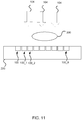
FIG. 11 illustrates a schematic representation of a cross section of adetector 200 having an array oftiles 100 according to an embodiment.X-ray radiation 104 is emitted from a source (not shown inFIG. 11 ). Anobject 300 to be detected and inspected by thex-ray radiation 104 is shown between the radiation source and thedetector 200. Thedetector 200 comprises an array having nine tiles 100 - 100_8 in the cross section of thedetector 200, for example in the x-axis direction. -
FIG. 11 illustrates thedetection devices 200 comprising atile 100 having asymmetrically positioned guardring contact pads 107 according to the embodiments. Thedevice 200 may be a part of an imaging system for detecting theobject 300, comprising thetile 100 as described in any of these embodiments. The system may be applied for example in medical imaging, security imaging and/or industrial imaging. - Any range or device value given herein may be extended or altered without losing the effect sought. Also any embodiment may be combined with another embodiment unless explicitly disallowed.
- Although the subject matter has been described in language specific to structural features and/or acts, it is to be understood that the subject matter defined in the appended claims is not necessarily limited to the specific features or acts described above. Rather, the specific features and acts described above are disclosed as examples of implementing the claims and other equivalent features and acts are intended to be within the scope of the claims.
- An embodiment relates to a device, comprising: a direct conversion compound semiconductor layer configured to convert x-ray photons into an electric current, the direct conversion compound semiconductor layer, comprising: a pixel array positioned on the direct conversion compound semiconductor layer, including pixels located at an outermost circumference; a guard ring encircling the pixel array, wherein the pixels at the outermost circumference are closest to the guard ring; guard ring contact pads, wherein the guard ring contact pads are situated at the outermost circumference and connected to the guard ring; wherein the guard ring contact pads are further situated asymmetrically with respect to a symmetry x-axis and a symmetry y-axis of the direct conversion compound semiconductor layer.
- Alternatively or in addition to the above, the guard ring contact pads are situated asymmetrically so that, when another direct conversion compound semiconductor layer is positioned next to the direct conversion compound semiconductor layer, the guard ring contact pads, which are separated by a gap between the layers, are not situated on an x-axis or a y-axis of one of the pads. Alternatively or in addition to the above, the guard ring contact pads are situated asymmetrically so that, when another direct conversion compound semiconductor layer is positioned next to the direct conversion compound semiconductor layer so that the sides of the direct conversion compound semiconductor layers are against each other, the guard ring contact pads situated at the sides are not situated on an x-axis or a y-axis crossing one of the pads. Alternatively or in addition to the above, the direct conversion compound semiconductor layer comprises a room temperature semiconductor layer. Alternatively or in addition to the above, the direct conversion compound semiconductor layer comprises a cadmium telluride layer or a cadmium zinc telluride sensor. Alternatively or in addition to the above, each side of the semiconductor layer includes at least one guard ring contact pad. Alternatively or in addition to the above, the guard ring contact pad is configured to ground the guard ring. Alternatively or in addition to the above, the pixels comprise signal pads. Alternatively or in addition to the above, the guard ring contact pad corresponds to a dead pixel in digital imaging. Alternatively or in addition to the above, further including an integrated circuit, IC, layer situated under the direct conversion compound semiconductor layer. Alternatively or in addition to the above, the guard ring contact pad connects the guard ring through the direct conversion compound semiconductor layer to the IC layer. Alternatively or in addition to the above, further including a substrate layer situated under the IC layer.
- According to an embodiment, the device comprises a tile. According to an embodiment, the detector comprises an array of tiles. According to an embodiment, an imaging system, comprising: an x-ray source; and the detector.
- It will be understood that the benefits and advantages described above may relate to one embodiment or may relate to several embodiments. The embodiments are not limited to those that solve any or all of the stated problems or those that have any or all of the stated benefits and advantages. It will further be understood that reference to 'an' item refers to one or more of those items.
- The steps of the methods described herein may be carried out in any suitable order, or simultaneously where appropriate. Additionally, individual blocks may be deleted from any of the methods without departing from the spirit and scope of the subject matter described herein. Aspects of any of the embodiments described above may be combined with aspects of any of the other embodiments described to form further embodiments without losing the effect sought.
- The term 'comprising' is used herein to mean including the method, blocks or elements identified, but that such blocks or elements do not comprise an exclusive list and a method or apparatus may contain additional blocks or elements.
- It will be understood that the above description is given by way of example only and that various modifications may be made by those skilled in the art. The above specification, embodiments and data provide a complete description of the structure and use of exemplary embodiments. Although various embodiments have been described above with a certain degree of particularity, or with reference to one or more individual embodiments, those skilled in the art could make numerous alterations to the disclosed embodiments without departing from the spirit or scope of this specification.
Claims (15)
- A device, comprising:a direct conversion compound semiconductor layer configured to convert high energy radiation photons into an electric current, the direct conversion compound semiconductor layer, comprising:a pixel array positioned on the direct conversion compound semiconductor layer, including pixels located at an outermost circumference;a guard ring encircling the pixel array, wherein the pixels at the outermost circumference are closest to the guard ring;guard ring contact pads, wherein the guard ring contact pads are situated at the outermost circumference and connected to the guard ring;wherein the guard ring contact pads are further situated asymmetrically with respect to a symmetry x-axis and a symmetry y-axis of the direct conversion compound semiconductor layer.
- The device of claim 1, wherein the guard ring contact pads are situated asymmetrically so that, when another direct conversion compound semiconductor layer is positioned next to the direct conversion compound semiconductor layer, the guard ring contact pads, which are separated by a gap between the layers, are not situated on an x-axis or a y-axis of one of the pads.
- The device of any preceding claim, wherein the guard ring contact pads are situated asymmetrically so that, when another direct conversion compound semiconductor layer is positioned next to the direct conversion compound semiconductor layer so that the sides of the direct conversion compound semiconductor layers are against each other, the guard ring contact pads situated at the sides are not situated on an x-axis or a y-axis crossing one of the pads.
- The device of any preceding claim, wherein the direct conversion compound semiconductor layer comprises a room temperature semiconductor layer.
- The device of any preceding claim, wherein the direct conversion compound semiconductor layer comprises a cadmium telluride layer or a cadmium zinc telluride sensor.
- The device of any preceding claim, wherein each side of the semiconductor layer includes at least one guard ring contact pad.
- The device of any preceding claim, wherein the guard ring contact pad is configured to ground the guard ring.
- The device of any preceding claim, wherein the pixels comprise signal pads.
- The device of any preceding claim, wherein the guard ring contact pad corresponds to a dead pixel in digital imaging.
- The device of any preceding claim, further including an integrated circuit, IC, layer situated under the direct conversion compound semiconductor layer.
- The device of any preceding claim, wherein the guard ring contact pad connects the guard ring through the direct conversion compound semiconductor layer to the IC layer.
- The device of any preceding claim, further including a substrate layer situated under the IC layer.
- The device of any preceding claim, wherein the device comprises a tile.
- A detector comprising an array of tiles according to any preceding claim.
- An imaging system, comprising:a high energy radiation source; andthe detector according to any preceding claim.
Priority Applications (5)
| Application Number | Priority Date | Filing Date | Title |
|---|---|---|---|
| EP17153477.9A EP3355355B1 (en) | 2017-01-27 | 2017-01-27 | Asymmetrically positioned guard ring contacts |
| CN201880008955.8A CN110268524B (en) | 2017-01-27 | 2018-01-25 | Asymmetrically positioned guard ring contacts |
| PCT/EP2018/051767 WO2018138176A1 (en) | 2017-01-27 | 2018-01-25 | Asymmetrically positioned guard ring contacts |
| JP2019534960A JP7050073B2 (en) | 2017-01-27 | 2018-01-25 | Devices, detectors, and image processing systems with asymmetrically placed guard ring contacts |
| US16/480,366 US11251214B2 (en) | 2017-01-27 | 2018-01-25 | Asymmetrically positioned guard ring contacts |
Applications Claiming Priority (1)
| Application Number | Priority Date | Filing Date | Title |
|---|---|---|---|
| EP17153477.9A EP3355355B1 (en) | 2017-01-27 | 2017-01-27 | Asymmetrically positioned guard ring contacts |
Publications (2)
| Publication Number | Publication Date |
|---|---|
| EP3355355A1 true EP3355355A1 (en) | 2018-08-01 |
| EP3355355B1 EP3355355B1 (en) | 2019-03-13 |
Family
ID=57914827
Family Applications (1)
| Application Number | Title | Priority Date | Filing Date |
|---|---|---|---|
| EP17153477.9A Active EP3355355B1 (en) | 2017-01-27 | 2017-01-27 | Asymmetrically positioned guard ring contacts |
Country Status (5)
| Country | Link |
|---|---|
| US (1) | US11251214B2 (en) |
| EP (1) | EP3355355B1 (en) |
| JP (1) | JP7050073B2 (en) |
| CN (1) | CN110268524B (en) |
| WO (1) | WO2018138176A1 (en) |
Citations (4)
| Publication number | Priority date | Publication date | Assignee | Title |
|---|---|---|---|---|
| GB2289983A (en) * | 1994-06-01 | 1995-12-06 | Simage Oy | Imaging devices systems and methods |
| US6037609A (en) * | 1997-01-17 | 2000-03-14 | General Electric Company | Corrosion resistant imager |
| JP2004303878A (en) * | 2003-03-31 | 2004-10-28 | Nippon Sheet Glass Co Ltd | Photodetector array |
| US20150069252A1 (en) * | 2013-09-09 | 2015-03-12 | Siemens Aktiengesellschaft | X-ray detector and method |
Family Cites Families (27)
| Publication number | Priority date | Publication date | Assignee | Title |
|---|---|---|---|---|
| US5227635A (en) * | 1991-11-22 | 1993-07-13 | Xsirious, Inc. | Mercuric iodide x-ray detector |
| US6046454A (en) * | 1995-10-13 | 2000-04-04 | Digirad Corporation | Semiconductor radiation detector with enhanced charge collection |
| US5677539A (en) * | 1995-10-13 | 1997-10-14 | Digirad | Semiconductor radiation detector with enhanced charge collection |
| US5943388A (en) * | 1996-07-30 | 1999-08-24 | Nova R & D, Inc. | Radiation detector and non-destructive inspection |
| DE69832761T2 (en) * | 1997-01-17 | 2006-11-02 | General Electric Co. | CORROSION-RESISTANT IMAGE RECORDING DEVICE |
| GB2335540B (en) * | 1998-03-20 | 2002-01-02 | Simage Oy | Imaging device for imaging radiation |
| US8120683B1 (en) * | 1999-04-08 | 2012-02-21 | Nova R & D, Inc. | High resoultion digital imaging apparatus |
| US6465824B1 (en) * | 2000-03-09 | 2002-10-15 | General Electric Company | Imager structure |
| JP3740390B2 (en) | 2000-07-10 | 2006-02-01 | キヤノン株式会社 | Imaging apparatus, radiation imaging apparatus, and radiation imaging system using the same |
| JP4280024B2 (en) * | 2001-04-23 | 2009-06-17 | 株式会社東芝 | X-ray flat panel detector |
| DE10244177A1 (en) * | 2002-09-23 | 2004-04-08 | Siemens Ag | Photosensitive screen for taking X-ray pictures has top fluorescent layer on contact layer on top of photosensor array with individual contacts on substrate with further contacts to circuit elements |
| US6928144B2 (en) * | 2003-08-01 | 2005-08-09 | General Electric Company | Guard ring for direct photo-to-electron conversion detector array |
| JP2008514965A (en) * | 2004-09-30 | 2008-05-08 | スタンフォード ユニバーシティ | Semiconductor crystal high-resolution imaging device |
| US20070072332A1 (en) * | 2005-09-26 | 2007-03-29 | Josef Kemmer | Semiconductor radiation detectors and method for fabrication thereof |
| JP4881071B2 (en) * | 2006-05-30 | 2012-02-22 | 株式会社日立製作所 | Radiation detector and radiation imaging apparatus equipped with the same |
| CN102203636B (en) | 2008-09-23 | 2013-07-31 | 达尔特斯能源物理学院 | Device for detecting highly energetic photons |
| US20110006389A1 (en) * | 2009-07-08 | 2011-01-13 | Lsi Corporation | Suppressing fractures in diced integrated circuits |
| JP5630027B2 (en) * | 2010-01-29 | 2014-11-26 | ソニー株式会社 | Solid-state imaging device, manufacturing method thereof, electronic apparatus, and semiconductor device |
| JP2012178496A (en) * | 2011-02-28 | 2012-09-13 | Sony Corp | Solid state image pickup device, electronic apparatus, semiconductor device, manufacturing method of solid state image pickup device |
| JP5774708B2 (en) * | 2011-08-24 | 2015-09-09 | ルネサスエレクトロニクス株式会社 | Semiconductor device |
| JP2013197113A (en) * | 2012-03-15 | 2013-09-30 | Sony Corp | Solid-state imaging device and camera system |
| FR2993097B1 (en) * | 2012-07-05 | 2015-05-22 | Commissariat Energie Atomique | CMOS IMAGER DEVICE WITH OPTIMIZED GEOMETRY AND METHOD OF MAKING SUCH A DEVICE BY PHOTOCOMPOSITION |
| KR20150106420A (en) * | 2013-01-11 | 2015-09-21 | 르네사스 일렉트로닉스 가부시키가이샤 | Semiconductor device |
| JP6120094B2 (en) * | 2013-07-05 | 2017-04-26 | ソニー株式会社 | Solid-state imaging device, manufacturing method thereof, and electronic apparatus |
| JP6192598B2 (en) * | 2014-06-19 | 2017-09-06 | ルネサスエレクトロニクス株式会社 | Imaging device and manufacturing method thereof |
| US20160148965A1 (en) * | 2014-09-30 | 2016-05-26 | James E. Clayton | Detector assembly using vertical wire bonds and compression decals |
| WO2017037527A1 (en) * | 2015-08-31 | 2017-03-09 | G-Ray Switzerland Sa | Photon counting cone-beam ct apparatus with monolithic cmos integrated pixel detectors |
-
2017
- 2017-01-27 EP EP17153477.9A patent/EP3355355B1/en active Active
-
2018
- 2018-01-25 JP JP2019534960A patent/JP7050073B2/en active Active
- 2018-01-25 US US16/480,366 patent/US11251214B2/en active Active
- 2018-01-25 CN CN201880008955.8A patent/CN110268524B/en active Active
- 2018-01-25 WO PCT/EP2018/051767 patent/WO2018138176A1/en active Application Filing
Patent Citations (4)
| Publication number | Priority date | Publication date | Assignee | Title |
|---|---|---|---|---|
| GB2289983A (en) * | 1994-06-01 | 1995-12-06 | Simage Oy | Imaging devices systems and methods |
| US6037609A (en) * | 1997-01-17 | 2000-03-14 | General Electric Company | Corrosion resistant imager |
| JP2004303878A (en) * | 2003-03-31 | 2004-10-28 | Nippon Sheet Glass Co Ltd | Photodetector array |
| US20150069252A1 (en) * | 2013-09-09 | 2015-03-12 | Siemens Aktiengesellschaft | X-ray detector and method |
Also Published As
| Publication number | Publication date |
|---|---|
| JP7050073B2 (en) | 2022-04-07 |
| CN110268524A (en) | 2019-09-20 |
| CN110268524B (en) | 2023-06-27 |
| US11251214B2 (en) | 2022-02-15 |
| JP2020507061A (en) | 2020-03-05 |
| WO2018138176A1 (en) | 2018-08-02 |
| EP3355355B1 (en) | 2019-03-13 |
| US20190386055A1 (en) | 2019-12-19 |
Similar Documents
| Publication | Publication Date | Title |
|---|---|---|
| US10153310B2 (en) | Stacked-chip backside-illuminated SPAD sensor with high fill-factor | |
| US7920195B2 (en) | Image sensing apparatus having an effective pixel area | |
| US9808159B2 (en) | Solid-state image sensor and imaging apparatus including the same | |
| US20180026147A1 (en) | Vertical gate guard ring for single photon avalanche diode pitch minimization | |
| ITVA20100026A1 (en) | METHOD OF DETECTION OF POSITIONS OF PHOTONS THAT MIX ON A GEIGER-MODE AVALANCHE PHOTODIODO, RELATED AVAILABLE GEIGER-MODE PHOTODIODS AND MANUFACTURING PROCESS | |
| US11658197B2 (en) | Photoelectric conversion apparatus, photoelectric conversion system, and moving object | |
| US9391111B1 (en) | Stacked integrated circuit system with thinned intermediate semiconductor die | |
| US11251214B2 (en) | Asymmetrically positioned guard ring contacts | |
| CN106324649B (en) | semiconductor detector | |
| US10942284B2 (en) | Radiation detector panel assembly structure | |
| US20210218912A1 (en) | Imaging device | |
| US20170221939A1 (en) | Functional element and electronic apparatus | |
| TW201830680A (en) | Stacked image sensor with shield bumps between interconnects | |
| US20140264710A1 (en) | Seal ring structure with rounded corners for semiconductor devices | |
| EP3142147B1 (en) | Image sensor and a method to manufacture thereof | |
| US20230290791A1 (en) | Imaging device | |
| US20200365742A1 (en) | Photodiode and x-ray sensor including the same | |
| JPS63185058A (en) | Solid-state image sensor |
Legal Events
| Date | Code | Title | Description |
|---|---|---|---|
| STAA | Information on the status of an ep patent application or granted ep patent |
Free format text: STATUS: EXAMINATION IS IN PROGRESS |
|
| PUAI | Public reference made under article 153(3) epc to a published international application that has entered the european phase |
Free format text: ORIGINAL CODE: 0009012 |
|
| 17P | Request for examination filed |
Effective date: 20170926 |
|
| AK | Designated contracting states |
Kind code of ref document: A1 Designated state(s): AL AT BE BG CH CY CZ DE DK EE ES FI FR GB GR HR HU IE IS IT LI LT LU LV MC MK MT NL NO PL PT RO RS SE SI SK SM TR |
|
| AX | Request for extension of the european patent |
Extension state: BA ME |
|
| GRAP | Despatch of communication of intention to grant a patent |
Free format text: ORIGINAL CODE: EPIDOSNIGR1 |
|
| STAA | Information on the status of an ep patent application or granted ep patent |
Free format text: STATUS: GRANT OF PATENT IS INTENDED |
|
| INTG | Intention to grant announced |
Effective date: 20180919 |
|
| RAP1 | Party data changed (applicant data changed or rights of an application transferred) |
Owner name: DETECTION TECHNOLOGY OY |
|
| GRAS | Grant fee paid |
Free format text: ORIGINAL CODE: EPIDOSNIGR3 |
|
| GRAA | (expected) grant |
Free format text: ORIGINAL CODE: 0009210 |
|
| STAA | Information on the status of an ep patent application or granted ep patent |
Free format text: STATUS: THE PATENT HAS BEEN GRANTED |
|
| AK | Designated contracting states |
Kind code of ref document: B1 Designated state(s): AL AT BE BG CH CY CZ DE DK EE ES FI FR GB GR HR HU IE IS IT LI LT LU LV MC MK MT NL NO PL PT RO RS SE SI SK SM TR |
|
| REG | Reference to a national code |
Ref country code: GB Ref legal event code: FG4D |
|
| REG | Reference to a national code |
Ref country code: CH Ref legal event code: EP Ref country code: AT Ref legal event code: REF Ref document number: 1108876 Country of ref document: AT Kind code of ref document: T Effective date: 20190315 |
|
| REG | Reference to a national code |
Ref country code: IE Ref legal event code: FG4D |
|
| REG | Reference to a national code |
Ref country code: DE Ref legal event code: R096 Ref document number: 602017002592 Country of ref document: DE |
|
| REG | Reference to a national code |
Ref country code: NL Ref legal event code: MP Effective date: 20190313 |
|
| REG | Reference to a national code |
Ref country code: LT Ref legal event code: MG4D |
|
| PG25 | Lapsed in a contracting state [announced via postgrant information from national office to epo] |
Ref country code: LT Free format text: LAPSE BECAUSE OF FAILURE TO SUBMIT A TRANSLATION OF THE DESCRIPTION OR TO PAY THE FEE WITHIN THE PRESCRIBED TIME-LIMIT Effective date: 20190313 Ref country code: SE Free format text: LAPSE BECAUSE OF FAILURE TO SUBMIT A TRANSLATION OF THE DESCRIPTION OR TO PAY THE FEE WITHIN THE PRESCRIBED TIME-LIMIT Effective date: 20190313 Ref country code: FI Free format text: LAPSE BECAUSE OF FAILURE TO SUBMIT A TRANSLATION OF THE DESCRIPTION OR TO PAY THE FEE WITHIN THE PRESCRIBED TIME-LIMIT Effective date: 20190313 Ref country code: NO Free format text: LAPSE BECAUSE OF FAILURE TO SUBMIT A TRANSLATION OF THE DESCRIPTION OR TO PAY THE FEE WITHIN THE PRESCRIBED TIME-LIMIT Effective date: 20190613 |
|
| PG25 | Lapsed in a contracting state [announced via postgrant information from national office to epo] |
Ref country code: GR Free format text: LAPSE BECAUSE OF FAILURE TO SUBMIT A TRANSLATION OF THE DESCRIPTION OR TO PAY THE FEE WITHIN THE PRESCRIBED TIME-LIMIT Effective date: 20190614 Ref country code: HR Free format text: LAPSE BECAUSE OF FAILURE TO SUBMIT A TRANSLATION OF THE DESCRIPTION OR TO PAY THE FEE WITHIN THE PRESCRIBED TIME-LIMIT Effective date: 20190313 Ref country code: RS Free format text: LAPSE BECAUSE OF FAILURE TO SUBMIT A TRANSLATION OF THE DESCRIPTION OR TO PAY THE FEE WITHIN THE PRESCRIBED TIME-LIMIT Effective date: 20190313 Ref country code: LV Free format text: LAPSE BECAUSE OF FAILURE TO SUBMIT A TRANSLATION OF THE DESCRIPTION OR TO PAY THE FEE WITHIN THE PRESCRIBED TIME-LIMIT Effective date: 20190313 Ref country code: NL Free format text: LAPSE BECAUSE OF FAILURE TO SUBMIT A TRANSLATION OF THE DESCRIPTION OR TO PAY THE FEE WITHIN THE PRESCRIBED TIME-LIMIT Effective date: 20190313 Ref country code: BG Free format text: LAPSE BECAUSE OF FAILURE TO SUBMIT A TRANSLATION OF THE DESCRIPTION OR TO PAY THE FEE WITHIN THE PRESCRIBED TIME-LIMIT Effective date: 20190613 |
|
| REG | Reference to a national code |
Ref country code: AT Ref legal event code: MK05 Ref document number: 1108876 Country of ref document: AT Kind code of ref document: T Effective date: 20190313 |
|
| PG25 | Lapsed in a contracting state [announced via postgrant information from national office to epo] |
Ref country code: ES Free format text: LAPSE BECAUSE OF FAILURE TO SUBMIT A TRANSLATION OF THE DESCRIPTION OR TO PAY THE FEE WITHIN THE PRESCRIBED TIME-LIMIT Effective date: 20190313 Ref country code: IT Free format text: LAPSE BECAUSE OF FAILURE TO SUBMIT A TRANSLATION OF THE DESCRIPTION OR TO PAY THE FEE WITHIN THE PRESCRIBED TIME-LIMIT Effective date: 20190313 Ref country code: RO Free format text: LAPSE BECAUSE OF FAILURE TO SUBMIT A TRANSLATION OF THE DESCRIPTION OR TO PAY THE FEE WITHIN THE PRESCRIBED TIME-LIMIT Effective date: 20190313 Ref country code: CZ Free format text: LAPSE BECAUSE OF FAILURE TO SUBMIT A TRANSLATION OF THE DESCRIPTION OR TO PAY THE FEE WITHIN THE PRESCRIBED TIME-LIMIT Effective date: 20190313 Ref country code: EE Free format text: LAPSE BECAUSE OF FAILURE TO SUBMIT A TRANSLATION OF THE DESCRIPTION OR TO PAY THE FEE WITHIN THE PRESCRIBED TIME-LIMIT Effective date: 20190313 Ref country code: PT Free format text: LAPSE BECAUSE OF FAILURE TO SUBMIT A TRANSLATION OF THE DESCRIPTION OR TO PAY THE FEE WITHIN THE PRESCRIBED TIME-LIMIT Effective date: 20190713 Ref country code: SK Free format text: LAPSE BECAUSE OF FAILURE TO SUBMIT A TRANSLATION OF THE DESCRIPTION OR TO PAY THE FEE WITHIN THE PRESCRIBED TIME-LIMIT Effective date: 20190313 Ref country code: AL Free format text: LAPSE BECAUSE OF FAILURE TO SUBMIT A TRANSLATION OF THE DESCRIPTION OR TO PAY THE FEE WITHIN THE PRESCRIBED TIME-LIMIT Effective date: 20190313 |
|
| PG25 | Lapsed in a contracting state [announced via postgrant information from national office to epo] |
Ref country code: PL Free format text: LAPSE BECAUSE OF FAILURE TO SUBMIT A TRANSLATION OF THE DESCRIPTION OR TO PAY THE FEE WITHIN THE PRESCRIBED TIME-LIMIT Effective date: 20190313 Ref country code: SM Free format text: LAPSE BECAUSE OF FAILURE TO SUBMIT A TRANSLATION OF THE DESCRIPTION OR TO PAY THE FEE WITHIN THE PRESCRIBED TIME-LIMIT Effective date: 20190313 |
|
| REG | Reference to a national code |
Ref country code: DE Ref legal event code: R097 Ref document number: 602017002592 Country of ref document: DE |
|
| PG25 | Lapsed in a contracting state [announced via postgrant information from national office to epo] |
Ref country code: IS Free format text: LAPSE BECAUSE OF FAILURE TO SUBMIT A TRANSLATION OF THE DESCRIPTION OR TO PAY THE FEE WITHIN THE PRESCRIBED TIME-LIMIT Effective date: 20190713 Ref country code: AT Free format text: LAPSE BECAUSE OF FAILURE TO SUBMIT A TRANSLATION OF THE DESCRIPTION OR TO PAY THE FEE WITHIN THE PRESCRIBED TIME-LIMIT Effective date: 20190313 |
|
| PLBE | No opposition filed within time limit |
Free format text: ORIGINAL CODE: 0009261 |
|
| STAA | Information on the status of an ep patent application or granted ep patent |
Free format text: STATUS: NO OPPOSITION FILED WITHIN TIME LIMIT |
|
| PG25 | Lapsed in a contracting state [announced via postgrant information from national office to epo] |
Ref country code: DK Free format text: LAPSE BECAUSE OF FAILURE TO SUBMIT A TRANSLATION OF THE DESCRIPTION OR TO PAY THE FEE WITHIN THE PRESCRIBED TIME-LIMIT Effective date: 20190313 |
|
| 26N | No opposition filed |
Effective date: 20191216 |
|
| PG25 | Lapsed in a contracting state [announced via postgrant information from national office to epo] |
Ref country code: TR Free format text: LAPSE BECAUSE OF FAILURE TO SUBMIT A TRANSLATION OF THE DESCRIPTION OR TO PAY THE FEE WITHIN THE PRESCRIBED TIME-LIMIT Effective date: 20190313 |
|
| PG25 | Lapsed in a contracting state [announced via postgrant information from national office to epo] |
Ref country code: MC Free format text: LAPSE BECAUSE OF FAILURE TO SUBMIT A TRANSLATION OF THE DESCRIPTION OR TO PAY THE FEE WITHIN THE PRESCRIBED TIME-LIMIT Effective date: 20190313 |
|
| REG | Reference to a national code |
Ref country code: CH Ref legal event code: PL |
|
| REG | Reference to a national code |
Ref country code: BE Ref legal event code: MM Effective date: 20200131 |
|
| PG25 | Lapsed in a contracting state [announced via postgrant information from national office to epo] |
Ref country code: LU Free format text: LAPSE BECAUSE OF NON-PAYMENT OF DUE FEES Effective date: 20200127 |
|
| PG25 | Lapsed in a contracting state [announced via postgrant information from national office to epo] |
Ref country code: BE Free format text: LAPSE BECAUSE OF NON-PAYMENT OF DUE FEES Effective date: 20200131 Ref country code: CH Free format text: LAPSE BECAUSE OF NON-PAYMENT OF DUE FEES Effective date: 20200131 Ref country code: LI Free format text: LAPSE BECAUSE OF NON-PAYMENT OF DUE FEES Effective date: 20200131 |
|
| PG25 | Lapsed in a contracting state [announced via postgrant information from national office to epo] |
Ref country code: IE Free format text: LAPSE BECAUSE OF NON-PAYMENT OF DUE FEES Effective date: 20200127 |
|
| PG25 | Lapsed in a contracting state [announced via postgrant information from national office to epo] |
Ref country code: MT Free format text: LAPSE BECAUSE OF FAILURE TO SUBMIT A TRANSLATION OF THE DESCRIPTION OR TO PAY THE FEE WITHIN THE PRESCRIBED TIME-LIMIT Effective date: 20190313 Ref country code: CY Free format text: LAPSE BECAUSE OF FAILURE TO SUBMIT A TRANSLATION OF THE DESCRIPTION OR TO PAY THE FEE WITHIN THE PRESCRIBED TIME-LIMIT Effective date: 20190313 |
|
| PG25 | Lapsed in a contracting state [announced via postgrant information from national office to epo] |
Ref country code: MK Free format text: LAPSE BECAUSE OF FAILURE TO SUBMIT A TRANSLATION OF THE DESCRIPTION OR TO PAY THE FEE WITHIN THE PRESCRIBED TIME-LIMIT Effective date: 20190313 |
|
| PGFP | Annual fee paid to national office [announced via postgrant information from national office to epo] |
Ref country code: FR Payment date: 20230120 Year of fee payment: 7 |
|
| PGFP | Annual fee paid to national office [announced via postgrant information from national office to epo] |
Ref country code: GB Payment date: 20230125 Year of fee payment: 7 Ref country code: DE Payment date: 20230119 Year of fee payment: 7 |
|
| PG25 | Lapsed in a contracting state [announced via postgrant information from national office to epo] |
Ref country code: SI Free format text: LAPSE BECAUSE OF FAILURE TO SUBMIT A TRANSLATION OF THE DESCRIPTION OR TO PAY THE FEE WITHIN THE PRESCRIBED TIME-LIMIT Effective date: 20190313 |