EP3355317A1 - Conductive light-transmissive film - Google Patents
Conductive light-transmissive film Download PDFInfo
- Publication number
- EP3355317A1 EP3355317A1 EP17796334.5A EP17796334A EP3355317A1 EP 3355317 A1 EP3355317 A1 EP 3355317A1 EP 17796334 A EP17796334 A EP 17796334A EP 3355317 A1 EP3355317 A1 EP 3355317A1
- Authority
- EP
- European Patent Office
- Prior art keywords
- transparent film
- layer
- conductive
- conductive transparent
- film according
- Prior art date
- Legal status (The legal status is an assumption and is not a legal conclusion. Google has not performed a legal analysis and makes no representation as to the accuracy of the status listed.)
- Granted
Links
Images
Classifications
-
- H—ELECTRICITY
- H01—ELECTRIC ELEMENTS
- H01B—CABLES; CONDUCTORS; INSULATORS; SELECTION OF MATERIALS FOR THEIR CONDUCTIVE, INSULATING OR DIELECTRIC PROPERTIES
- H01B5/00—Non-insulated conductors or conductive bodies characterised by their form
- H01B5/14—Non-insulated conductors or conductive bodies characterised by their form comprising conductive layers or films on insulating-supports
-
- B—PERFORMING OPERATIONS; TRANSPORTING
- B32—LAYERED PRODUCTS
- B32B—LAYERED PRODUCTS, i.e. PRODUCTS BUILT-UP OF STRATA OF FLAT OR NON-FLAT, e.g. CELLULAR OR HONEYCOMB, FORM
- B32B7/00—Layered products characterised by the relation between layers; Layered products characterised by the relative orientation of features between layers, or by the relative values of a measurable parameter between layers, i.e. products comprising layers having different physical, chemical or physicochemical properties; Layered products characterised by the interconnection of layers
-
- C—CHEMISTRY; METALLURGY
- C09—DYES; PAINTS; POLISHES; NATURAL RESINS; ADHESIVES; COMPOSITIONS NOT OTHERWISE PROVIDED FOR; APPLICATIONS OF MATERIALS NOT OTHERWISE PROVIDED FOR
- C09D—COATING COMPOSITIONS, e.g. PAINTS, VARNISHES OR LACQUERS; FILLING PASTES; CHEMICAL PAINT OR INK REMOVERS; INKS; CORRECTING FLUIDS; WOODSTAINS; PASTES OR SOLIDS FOR COLOURING OR PRINTING; USE OF MATERIALS THEREFOR
- C09D201/00—Coating compositions based on unspecified macromolecular compounds
-
- C—CHEMISTRY; METALLURGY
- C09—DYES; PAINTS; POLISHES; NATURAL RESINS; ADHESIVES; COMPOSITIONS NOT OTHERWISE PROVIDED FOR; APPLICATIONS OF MATERIALS NOT OTHERWISE PROVIDED FOR
- C09D—COATING COMPOSITIONS, e.g. PAINTS, VARNISHES OR LACQUERS; FILLING PASTES; CHEMICAL PAINT OR INK REMOVERS; INKS; CORRECTING FLUIDS; WOODSTAINS; PASTES OR SOLIDS FOR COLOURING OR PRINTING; USE OF MATERIALS THEREFOR
- C09D7/00—Features of coating compositions, not provided for in group C09D5/00; Processes for incorporating ingredients in coating compositions
- C09D7/40—Additives
-
- C—CHEMISTRY; METALLURGY
- C09—DYES; PAINTS; POLISHES; NATURAL RESINS; ADHESIVES; COMPOSITIONS NOT OTHERWISE PROVIDED FOR; APPLICATIONS OF MATERIALS NOT OTHERWISE PROVIDED FOR
- C09D—COATING COMPOSITIONS, e.g. PAINTS, VARNISHES OR LACQUERS; FILLING PASTES; CHEMICAL PAINT OR INK REMOVERS; INKS; CORRECTING FLUIDS; WOODSTAINS; PASTES OR SOLIDS FOR COLOURING OR PRINTING; USE OF MATERIALS THEREFOR
- C09D7/00—Features of coating compositions, not provided for in group C09D5/00; Processes for incorporating ingredients in coating compositions
- C09D7/40—Additives
- C09D7/60—Additives non-macromolecular
- C09D7/61—Additives non-macromolecular inorganic
-
- C—CHEMISTRY; METALLURGY
- C23—COATING METALLIC MATERIAL; COATING MATERIAL WITH METALLIC MATERIAL; CHEMICAL SURFACE TREATMENT; DIFFUSION TREATMENT OF METALLIC MATERIAL; COATING BY VACUUM EVAPORATION, BY SPUTTERING, BY ION IMPLANTATION OR BY CHEMICAL VAPOUR DEPOSITION, IN GENERAL; INHIBITING CORROSION OF METALLIC MATERIAL OR INCRUSTATION IN GENERAL
- C23C—COATING METALLIC MATERIAL; COATING MATERIAL WITH METALLIC MATERIAL; SURFACE TREATMENT OF METALLIC MATERIAL BY DIFFUSION INTO THE SURFACE, BY CHEMICAL CONVERSION OR SUBSTITUTION; COATING BY VACUUM EVAPORATION, BY SPUTTERING, BY ION IMPLANTATION OR BY CHEMICAL VAPOUR DEPOSITION, IN GENERAL
- C23C14/00—Coating by vacuum evaporation, by sputtering or by ion implantation of the coating forming material
- C23C14/06—Coating by vacuum evaporation, by sputtering or by ion implantation of the coating forming material characterised by the coating material
- C23C14/08—Oxides
-
- C—CHEMISTRY; METALLURGY
- C23—COATING METALLIC MATERIAL; COATING MATERIAL WITH METALLIC MATERIAL; CHEMICAL SURFACE TREATMENT; DIFFUSION TREATMENT OF METALLIC MATERIAL; COATING BY VACUUM EVAPORATION, BY SPUTTERING, BY ION IMPLANTATION OR BY CHEMICAL VAPOUR DEPOSITION, IN GENERAL; INHIBITING CORROSION OF METALLIC MATERIAL OR INCRUSTATION IN GENERAL
- C23C—COATING METALLIC MATERIAL; COATING MATERIAL WITH METALLIC MATERIAL; SURFACE TREATMENT OF METALLIC MATERIAL BY DIFFUSION INTO THE SURFACE, BY CHEMICAL CONVERSION OR SUBSTITUTION; COATING BY VACUUM EVAPORATION, BY SPUTTERING, BY ION IMPLANTATION OR BY CHEMICAL VAPOUR DEPOSITION, IN GENERAL
- C23C14/00—Coating by vacuum evaporation, by sputtering or by ion implantation of the coating forming material
- C23C14/22—Coating by vacuum evaporation, by sputtering or by ion implantation of the coating forming material characterised by the process of coating
- C23C14/34—Sputtering
-
- G—PHYSICS
- G06—COMPUTING OR CALCULATING; COUNTING
- G06F—ELECTRIC DIGITAL DATA PROCESSING
- G06F3/00—Input arrangements for transferring data to be processed into a form capable of being handled by the computer; Output arrangements for transferring data from processing unit to output unit, e.g. interface arrangements
- G06F3/01—Input arrangements or combined input and output arrangements for interaction between user and computer
- G06F3/03—Arrangements for converting the position or the displacement of a member into a coded form
- G06F3/041—Digitisers, e.g. for touch screens or touch pads, characterised by the transducing means
-
- H—ELECTRICITY
- H01—ELECTRIC ELEMENTS
- H01B—CABLES; CONDUCTORS; INSULATORS; SELECTION OF MATERIALS FOR THEIR CONDUCTIVE, INSULATING OR DIELECTRIC PROPERTIES
- H01B1/00—Conductors or conductive bodies characterised by the conductive materials; Selection of materials as conductors
- H01B1/02—Conductors or conductive bodies characterised by the conductive materials; Selection of materials as conductors mainly consisting of metals or alloys
-
- H—ELECTRICITY
- H01—ELECTRIC ELEMENTS
- H01B—CABLES; CONDUCTORS; INSULATORS; SELECTION OF MATERIALS FOR THEIR CONDUCTIVE, INSULATING OR DIELECTRIC PROPERTIES
- H01B13/00—Apparatus or processes specially adapted for manufacturing conductors or cables
- H01B13/0026—Apparatus for manufacturing conducting or semi-conducting layers, e.g. deposition of metal
-
- H—ELECTRICITY
- H05—ELECTRIC TECHNIQUES NOT OTHERWISE PROVIDED FOR
- H05B—ELECTRIC HEATING; ELECTRIC LIGHT SOURCES NOT OTHERWISE PROVIDED FOR; CIRCUIT ARRANGEMENTS FOR ELECTRIC LIGHT SOURCES, IN GENERAL
- H05B33/00—Electroluminescent light sources
- H05B33/12—Light sources with substantially two-dimensional [2D] radiating surfaces
- H05B33/26—Light sources with substantially two-dimensional [2D] radiating surfaces characterised by the composition or arrangement of the conductive material used as an electrode
- H05B33/28—Light sources with substantially two-dimensional [2D] radiating surfaces characterised by the composition or arrangement of the conductive material used as an electrode of translucent electrodes
-
- H—ELECTRICITY
- H05—ELECTRIC TECHNIQUES NOT OTHERWISE PROVIDED FOR
- H05K—PRINTED CIRCUITS; CASINGS OR CONSTRUCTIONAL DETAILS OF ELECTRIC APPARATUS; MANUFACTURE OF ASSEMBLAGES OF ELECTRICAL COMPONENTS
- H05K3/00—Apparatus or processes for manufacturing printed circuits
- H05K3/38—Improvement of the adhesion between the insulating substrate and the metal
- H05K3/388—Improvement of the adhesion between the insulating substrate and the metal by the use of a metallic or inorganic thin film adhesion layer
-
- B—PERFORMING OPERATIONS; TRANSPORTING
- B32—LAYERED PRODUCTS
- B32B—LAYERED PRODUCTS, i.e. PRODUCTS BUILT-UP OF STRATA OF FLAT OR NON-FLAT, e.g. CELLULAR OR HONEYCOMB, FORM
- B32B2307/00—Properties of the layers or laminate
- B32B2307/20—Properties of the layers or laminate having particular electrical or magnetic properties, e.g. piezoelectric
- B32B2307/202—Conductive
-
- B—PERFORMING OPERATIONS; TRANSPORTING
- B32—LAYERED PRODUCTS
- B32B—LAYERED PRODUCTS, i.e. PRODUCTS BUILT-UP OF STRATA OF FLAT OR NON-FLAT, e.g. CELLULAR OR HONEYCOMB, FORM
- B32B2307/00—Properties of the layers or laminate
- B32B2307/40—Properties of the layers or laminate having particular optical properties
- B32B2307/412—Transparent
-
- C—CHEMISTRY; METALLURGY
- C09—DYES; PAINTS; POLISHES; NATURAL RESINS; ADHESIVES; COMPOSITIONS NOT OTHERWISE PROVIDED FOR; APPLICATIONS OF MATERIALS NOT OTHERWISE PROVIDED FOR
- C09D—COATING COMPOSITIONS, e.g. PAINTS, VARNISHES OR LACQUERS; FILLING PASTES; CHEMICAL PAINT OR INK REMOVERS; INKS; CORRECTING FLUIDS; WOODSTAINS; PASTES OR SOLIDS FOR COLOURING OR PRINTING; USE OF MATERIALS THEREFOR
- C09D7/00—Features of coating compositions, not provided for in group C09D5/00; Processes for incorporating ingredients in coating compositions
- C09D7/40—Additives
- C09D7/60—Additives non-macromolecular
- C09D7/63—Additives non-macromolecular organic
-
- G—PHYSICS
- G06—COMPUTING OR CALCULATING; COUNTING
- G06F—ELECTRIC DIGITAL DATA PROCESSING
- G06F2203/00—Indexing scheme relating to G06F3/00 - G06F3/048
- G06F2203/041—Indexing scheme relating to G06F3/041 - G06F3/045
- G06F2203/04103—Manufacturing, i.e. details related to manufacturing processes specially suited for touch sensitive devices
-
- H—ELECTRICITY
- H01—ELECTRIC ELEMENTS
- H01B—CABLES; CONDUCTORS; INSULATORS; SELECTION OF MATERIALS FOR THEIR CONDUCTIVE, INSULATING OR DIELECTRIC PROPERTIES
- H01B1/00—Conductors or conductive bodies characterised by the conductive materials; Selection of materials as conductors
- H01B1/06—Conductors or conductive bodies characterised by the conductive materials; Selection of materials as conductors mainly consisting of other non-metallic substances
- H01B1/08—Conductors or conductive bodies characterised by the conductive materials; Selection of materials as conductors mainly consisting of other non-metallic substances oxides
-
- H—ELECTRICITY
- H05—ELECTRIC TECHNIQUES NOT OTHERWISE PROVIDED FOR
- H05K—PRINTED CIRCUITS; CASINGS OR CONSTRUCTIONAL DETAILS OF ELECTRIC APPARATUS; MANUFACTURE OF ASSEMBLAGES OF ELECTRICAL COMPONENTS
- H05K2201/00—Indexing scheme relating to printed circuits covered by H05K1/00
- H05K2201/01—Dielectrics
- H05K2201/0104—Properties and characteristics in general
- H05K2201/0108—Transparent
-
- H—ELECTRICITY
- H05—ELECTRIC TECHNIQUES NOT OTHERWISE PROVIDED FOR
- H05K—PRINTED CIRCUITS; CASINGS OR CONSTRUCTIONAL DETAILS OF ELECTRIC APPARATUS; MANUFACTURE OF ASSEMBLAGES OF ELECTRICAL COMPONENTS
- H05K2201/00—Indexing scheme relating to printed circuits covered by H05K1/00
- H05K2201/01—Dielectrics
- H05K2201/0137—Materials
- H05K2201/0145—Polyester, e.g. polyethylene terephthalate [PET], polyethylene naphthalate [PEN]
-
- H—ELECTRICITY
- H05—ELECTRIC TECHNIQUES NOT OTHERWISE PROVIDED FOR
- H05K—PRINTED CIRCUITS; CASINGS OR CONSTRUCTIONAL DETAILS OF ELECTRIC APPARATUS; MANUFACTURE OF ASSEMBLAGES OF ELECTRICAL COMPONENTS
- H05K2201/00—Indexing scheme relating to printed circuits covered by H05K1/00
- H05K2201/01—Dielectrics
- H05K2201/0137—Materials
- H05K2201/0158—Polyalkene or polyolefin, e.g. polyethylene [PE], polypropylene [PP]
-
- H—ELECTRICITY
- H05—ELECTRIC TECHNIQUES NOT OTHERWISE PROVIDED FOR
- H05K—PRINTED CIRCUITS; CASINGS OR CONSTRUCTIONAL DETAILS OF ELECTRIC APPARATUS; MANUFACTURE OF ASSEMBLAGES OF ELECTRICAL COMPONENTS
- H05K2201/00—Indexing scheme relating to printed circuits covered by H05K1/00
- H05K2201/03—Conductive materials
- H05K2201/032—Materials
- H05K2201/0326—Inorganic, non-metallic conductor, e.g. indium-tin oxide [ITO]
-
- H—ELECTRICITY
- H05—ELECTRIC TECHNIQUES NOT OTHERWISE PROVIDED FOR
- H05K—PRINTED CIRCUITS; CASINGS OR CONSTRUCTIONAL DETAILS OF ELECTRIC APPARATUS; MANUFACTURE OF ASSEMBLAGES OF ELECTRICAL COMPONENTS
- H05K2201/00—Indexing scheme relating to printed circuits covered by H05K1/00
- H05K2201/10—Details of components or other objects attached to or integrated in a printed circuit board
- H05K2201/10007—Types of components
- H05K2201/10128—Display
-
- H—ELECTRICITY
- H05—ELECTRIC TECHNIQUES NOT OTHERWISE PROVIDED FOR
- H05K—PRINTED CIRCUITS; CASINGS OR CONSTRUCTIONAL DETAILS OF ELECTRIC APPARATUS; MANUFACTURE OF ASSEMBLAGES OF ELECTRICAL COMPONENTS
- H05K3/00—Apparatus or processes for manufacturing printed circuits
- H05K3/02—Apparatus or processes for manufacturing printed circuits in which the conductive material is applied to the surface of the insulating support and is thereafter removed from such areas of the surface which are not intended for current conducting or shielding
- H05K3/022—Processes for manufacturing precursors of printed circuits, i.e. copper-clad substrates
Definitions
- the present application relates to a conductive transparent film.
- the conductive transparent film is generally configured so as to comprise a transparent base material and an ITO thin film (layer).
- the film thus configured can be used for an imaging device such as a display, a touch panel, or the like.
- an imaging device such as a display, a touch panel, or the like.
- the present application relates to a conductive transparent film.
- the film may have a light transmittance of 75% or more. More specifically, the film may have a light transmittance of 80% or more, 85% or more, or 90% or more.
- the term "light” in the present application may mean a visible light having a wavelength of 380 nm to 780 nm, more specifically, a visible light having a wavelength of 550 nm.
- the conductive transparent film may comprise a conductive layer, an undercoating layer, and an anti-crack buffer layer.
- the conductive layer may comprise a transparent conductive oxide.
- the transparent conductive oxide for example, ITO (indium tin oxide), In 2 O 3 (indium oxide), IGO (indium gallium oxide), FTO (fluor doped tin oxide), AZO (aluminum doped zinc oxide), GZO (gallium doped zinc oxide), ATO (antimony doped tin oxide), IZO (indium doped zinc oxide), NTO (niobium doped titanium oxide), ZnO (zinc oxide), or CTO (cesium tungsten oxide), and the like can be used.
- ITO indium tin oxide
- In 2 O 3 indium oxide
- IGO indium gallium oxide
- FTO fluor doped tin oxide
- AZO aluminum doped zinc oxide
- GZO gallium doped zinc oxide
- ATO antimony doped tin oxide
- IZO indium doped zinc oxide
- NTO niobium doped titanium oxide
- the conductive layer may comprise indium oxide as a transparent conductive oxide. More specifically, the conductive layer may comprise an indium-based composite oxide containing indium oxide and an oxide of a tetravalent metal.
- the oxide of the tetravalent metal may be represented by the following formula 1. [Formula 1] AO 2
- A may be a tetravalent metal selected from the group consisting of Sn, Zr, Ge, Ti, Ce, Nb, Ta, Mb and W.
- the oxide of the tetravalent metal represented by Formula 1 above may be included in an amount of 1 to 20 parts by weight relative to 100 parts by weight of the total indium-based composite oxide constituting the conductive layer.
- the term part by weight may mean a content ratio between the components. If the lower limit of the above range is not satisfied, the electrical characteristics of the conductive layer, for example, sheet resistance and conductivity are poor. In addition, when the upper limit of the above range is not satisfied, the crystallization temperature is increased and thus the process energy efficiency for forming the conductive layer is poor.
- the conductive layer may have a thickness of 100 nm or less. More specifically, the conductive layer may have a thickness of 80 nm or less, or 50 nm or less, and 5 nm or more, or 10 nm or more. When the thickness range is satisfied, a conductive layer having evenly excellent mechanical properties, transmittance and sheet resistance may be provided.
- the conductive layer may have an optical refraction index of 1.7 to 2.3.
- the undercoating layer may be a layer included for improving the optical characteristics of the conductive transparent film, that is, for increasing the visible light transmittance of the film.
- the optical refraction index of the undercoating layer may have a value different from the optical refraction index of the base material layer and/or the optical refraction index of the conductive layer. More specifically, the undercoating layer may have an optical refraction index in the range of 1.5 to 2.0 on the premise of being different from the optical refraction index of the base material layer and/or the optical refraction index of the conductive layer. When the above range and relationship are satisfied, the visible light transmittance of the conductive transparent film can be increased.
- the undercoating layer may comprise an organic substance, an inorganic substance, or a mixture thereof.
- the undercoating layer may comprise a resin capable of thermosetting or photo-curing as an organic substance.
- a resin capable of thermosetting or photo-curing as an organic substance.
- at least one from an acrylic resin, a urethane resin, a thiourethane resin, a melamine resin, an alkyd resin, a siloxane polymer and an organosilane compound represented by Formula 2 below may be used as an organic substance: [Formula 2] (R 1 ) m -Si-X (4-m) in Formula 2 above, R 1 may be the same or different from each other and is alkyl having 1 to 12 carbon atoms, alkenyl, alkynyl, aryl, arylalkyl, alkylaryl, arylalkenyl, alkenylaryl, arylalkynyl, alkynylaryl, halogen, substituted amino, amide, aldehyde, keto, alkylcarbonyl, carboxy, mer
- the organosilane compound as above when used in the undercoating layer, the organosilane compound may be cross-linkable and may be mixed with highly refractive particles to control the refractive index.
- the type of highly refractive particles is not particularly limited.
- the kind of the organosilane compound is not particularly limited.
- the undercoating layer may comprise an inorganic substance.
- an inorganic substance such as TiO 2 , Nb 2 O 5 , Ta 2 O 5 , Sb 2 O 5 , ZrO 2 , ZnO, ZnS or a metal alkoxide compound represented by the following formula 3 may be included in the undercoating layer.
- M represents a metal selected from the group consisting of aluminum, zirconium, titanium, and silicon
- R 3 may be the same or different from each other and is halogen, alkyl having 1 to 12 carbon atoms, alkoxy, acyloxy, or hydroxy and Z is an integer of 2 or 4.
- the organic substance may be contained in an amount of 0.001 to 100 parts by weight relative to 100 parts by weight of the entire mixture.
- the undercoating layer may have a thickness of 150 nm or less. Specifically, the undercoating layer may have a thickness of 130 nm or less, 110 nm or less, or 100 nm or less. When the thickness of the undercoating layer is more than 150 nm, transmittance and color difference index of the conductive transparent film may be lowered.
- the thickness lower limit of the undercoating layer is not particularly limited, but may be 1 nm or more in consideration of processability, or function of the undercoating layer.
- the conductive transparent film of the present application may further an anti-crack buffer layer.
- the anti-crack buffer layer may be positioned between the undercoating layer and the conductive layer.
- the anti-crack buffer layer can contribute to reduction of surface resistance of the conductive layer and improvement of interfacial adhesion between layers.
- the film of the present application can maintain a high level of transmittance corresponding to the above-described range.
- one surface of the undercoating layer is configured so as to be directly contacted with one surface of the conductive layer, that is, the conductive layer is directly formed on one surface of the undercoating layer
- the conductive layer has been frequently contaminated by the organic substance in the undercoating layer and thus a conductive layer having a resistance value of at least 100 ⁇ / ⁇ or more, usually 150 ⁇ / ⁇ or more, or 250 ⁇ / ⁇ or more has been generally used for the conductive transparent film.
- a conductive layer having a resistance value of at least 100 ⁇ / ⁇ or more, usually 150 ⁇ / ⁇ or more, or 250 ⁇ / ⁇ or more has been generally used for the conductive transparent film.
- considering the configuration generally used for the conductive transparent film it is not easy to lower the resistance value of the conductive layer.
- the conductive transparent film of the present application may comprise an anti-crack buffer layer between the undercoating layer and the conductive layer, thereby preventing contamination of the interface of the conductive layer by the organic substance used in the undercoating layer and lowering the resistance value of the conductive layer. As a result, the response speed can be improved.
- the conductive layer included in the conductive transparent film of the present application may have a surface resistance of 300 ⁇ / ⁇ or less, 200 ⁇ / ⁇ or less, 100 ⁇ / ⁇ or less, or 95 ⁇ / ⁇ or less.
- the lower the surface resistance value the faster the response speed can be achieved, and thus the lower limit of the surface resistance value of the conductive layer is not particularly limited, but may be, for example, 10 ⁇ / ⁇ or more or 20 ⁇ / ⁇ or more.
- the anti-crack buffer layer satisfying the following constitution is used, the optical characteristics of the film such as transparency do not deteriorate even if the layer structure is added.
- the anti-crack buffer layer may comprise a metal oxide. More specifically, the anti-crack buffer layer may comprise NbO x .
- X may have a value in the range of 1 to 2.5 as a content ratio between elements. With the above range, a predetermined effect, for example, thin film reliability, high transmittance, and excellent mechanical properties can be provided. Conversely, when the above range is not satisfied, the transmittance is lowered, and it is difficult to laminate it with other layers.
- the X may be measured using a known method, for example, XPS (X-ray photoelectron spectroscopy) or the like.
- the anti-crack buffer layer may have a thickness in a range of 0.1 nm to 20 nm. If the thickness of the anti-crack buffer layer is less than 0.1 nm, it is difficult to obtain effects such as reduction of the surface resistance by the buffer layer or increase of the interfacial adhesion, and if the thickness exceeds 20 nm, optical properties and mechanical properties may be deteriorated. In one example, considering the optical properties such as light transmittance and the mechanical properties such as crack prevention, the anti-crack buffer layer may be formed to have the thickness in the range of 0.1 nm to 5 nm or 0.5 nm to 3 nm.
- the anti-crack buffer layer has excellent interfacial adhesion to the undercoating layer and the conductive layer, it is possible to suppress the occurrence of cracks in the conductive transparent film and to improve the mechanical properties thereof. For example, since the anti-crack buffer layer has excellent interfacial adhesion, the occurrence degree of cracks generated in the conductive layer can be reduced, when an external pressure such as bending is applied to the conductive transparent film.
- the conductive transparent film of the present application may comprise a conductive layer having a crack density value of 80 cracks/mm 2 or less.
- the crack density may be a value measured by bending a specimen, in which the conductive transparent film is tailored to a size of 1 mm x 1 mm, with vernier calipers and then dividing the combined length value of the entire crack generated in the conductive layer by 100 ⁇ m. Since the value of the crack density becomes smaller as the interfacial adhesion is better, the lower limit of the crack density value is not particularly limited. In one example, the lower limit of the crack density value may be 1 crack/mm 2 or more, 5 cracks/mm 2 or more, or 10 cracks/mm 2 or more.
- the conductive transparent film may further comprise a base material (substrate layer).
- the conductive transparent film may comprise a base material, an undercoating layer, an anti-crack buffer layer, and a conductive layer in this order.
- the base material layer may comprise a flexible plastic film having transmittance. If it is optically transparent and flexible, the kind of the film used for the base material layer is not particularly limited.
- a polyester film such as a PC (polycarbonate) film or a PEN (poly(ethylene naphthalate)) film or a PET (poly(ethylene terephthalate)) film, an acrylic film such as a PMMA (poly(methyl methacrylate) film, a PA (polyamide) film, a PVC (poly(vinyl chloride)) film, a PS (polystyrene) film, a PES (poly(ethersulfone)) film, a PEI (poly(ether imide)) film, or a polyolefin film such as a PE (polyethylene) film or a PP (polypropylene) film, and the like may be used as the base material layer, without being limited thereto.
- separate treatment such as corona discharge treatment, ultraviolet irradiation treatment or plasma treatment may be performed on the surface of the base material layer, in order to improve the interfacial adhesion with the adjacent layer.
- the base material layer may have a thickness in the range of 5 ⁇ m to 150 ⁇ m. If the thickness is less than 5 ⁇ m, the mechanical strength may be poor, and if the thickness exceeds 150 ⁇ m, sensitivity of the touch panel may be poor.
- the base material layer may have an optical refraction index in a range of 1.4 to 1.7.
- the present application relates to a method for manufacturing a conductive transparent film.
- the manufacturing method may comprise a step of sequentially providing an anti-crack buffer layer and a conductive layer on an undercoating layer. Specific components and characteristics of the undercoating layer, the anti-crack buffer layer and the conductive layer are as explained above.
- the undercoating layer may be formed by applying an undercoating layer precursor composition onto a base material layer and then curing it.
- the composition may comprise the organic substance, the inorganic substance, or the mixture thereof, as described above.
- the curing conditions are not particularly limited and the known heat or photo-curing methods can be used.
- the anti-crack buffer layer and the conductive layer may be formed by vapor deposition.
- the deposition method is not particularly limited, and a physical vapor deposition (PVD) method such as a sputtering method or an E-beam evaporation method may be used.
- PVD physical vapor deposition
- the anti-crack buffer layer may be prepared through sputtering deposition.
- the x value which is a content ratio of niobium oxide (NbOx) forming the anti-crack buffer layer, may be adjusted to 1 to 2.5 by controlling the deposition process.
- the deposition process is controlled so as to satisfy the range X, an anti-crack buffer layer having excellent process efficiency and high thin film stability is provided.
- the conductive layer may also be prepared through sputtering deposition.
- a conductive layer can be formed by causing argon ions to impact an oxide composite target containing indium oxide and the tetravalent metal oxide at a process pressure of 1 mtorr to 30 mtorr and a temperature of 100°C to 500°C.
- the present application relates to a device comprising the conductive transparent film.
- the device may be a display, a lighting device, a touch panel, or the like.
- a conductive transparent film having not only excellent transmittance but also simultaneously improved mechanical properties and response speed.
- a protective film was attached to the conductive transparent film in the film form prepared in Examples and Comparative Examples, and the ITO layer was crystallized by heat treatment. Then, the film was cut into a size of 1 mm x 1 mm to prepare a specimen. When the specimen was placed in a bending state with vernier calipers so that the crystallized ITO layer was located on the inner side and maintained for 30 seconds, the bend length at the time when cracks were generated in the ITO layer was measured.
- the length of 100 ⁇ m was regarded as one crack, and the lengths of the entire crack generated in the specimen were combined, and then the combined value was divided by 100 ⁇ m. As a result, cracks having different lengths and numbers were quantified.
- a solution containing a condensable organosilane compound (methyltrimethoxysilane) was coated on a transparent PET base material having a thickness of 50 ⁇ m and thermally cured to form an undercoating layer having a thickness of 40 nm.
- An anti-crack buffer layer comprising niobium oxide (NbO x ) was deposited on the undercoating layer to a thickness of 1 nm by using a sputtering technique, while targeting niobium (Nb) and supplying a mixed gas of argon and oxygen to the deposition equipment.
- an indium oxide layer comprising SnO 2 was formed to a thickness of 21.3 nm on the anti-crack buffer layer using the sputtering technique to prepare a conductive transparent film.
- the constitution and physical properties of the prepared film are as shown in Tables 1 and 2, respectively.
- a film was prepared in the same manner as in Example 1, except for the thickness of the anti-crack buffer layer and the surface resistance value.
- the physical properties of the prepared film are as shown in Table 2.
- Example 1 As shown in Table 1 below, a film was prepared in the same manner as in Example 1, except that the ITO layer was directly formed on the undercoating layer, without preparing the anti-crack buffer layer.
- the physical properties of the prepared film are as shown in Table 2.
- ITO Thickness (nm) Composition of Anti-crack Buffer Layer Thickness of Anti-crack Buffer Layer (nm)
- Example 1 21.3 NbO 1.5 1
- Example 2 21.3 NbO 1.5 1.5
- Example 3 21.3 NbO 1.5 2
- Example 4 21.3 NbO 1.5 3
- Example 5 21.3 NbO 1.5 5 Comparative Example 1 21.3 - -
- Example 1 92 91.6 16 31.8
- Example 2 94 91.2 16 48.6
- Example 3 93 90.8 16 46.
Landscapes
- Chemical & Material Sciences (AREA)
- Engineering & Computer Science (AREA)
- Materials Engineering (AREA)
- Organic Chemistry (AREA)
- Life Sciences & Earth Sciences (AREA)
- Wood Science & Technology (AREA)
- Manufacturing & Machinery (AREA)
- Mechanical Engineering (AREA)
- Metallurgy (AREA)
- Chemical Kinetics & Catalysis (AREA)
- Theoretical Computer Science (AREA)
- General Engineering & Computer Science (AREA)
- Inorganic Chemistry (AREA)
- Microelectronics & Electronic Packaging (AREA)
- Human Computer Interaction (AREA)
- Physics & Mathematics (AREA)
- General Physics & Mathematics (AREA)
- Laminated Bodies (AREA)
- Non-Insulated Conductors (AREA)
Abstract
Description
- The present application claims the benefit of priority based on Korean Patent Application No.
2016-0056329 filed on May 9, 2016 2017-0056216 - The present application relates to a conductive transparent film.
- The conductive transparent film is generally configured so as to comprise a transparent base material and an ITO thin film (layer). The film thus configured can be used for an imaging device such as a display, a touch panel, or the like. In this regard, since the recent trend is enlargement of the display or touch panel area, it is important to lower specific resistance of the conductive transparent film and each component used therein.
- On the other hand, attempts have been made to improve the optical characteristics of the conductive transparent film through refractive index matching between the ITO layer and the transparent base material. For example, for the refractive index matching, a so-called undercoating layer may be placed between the ITO layer and the transparent base material. However, upon the deposition process for forming the ITO layer, the undercoating layer formed of the organic substance may be damaged, and the organic substance derived from the undercoating layer may contaminate the ITO layer, and thus there is a problem that the specific resistance of the ITO layer increases. Such an increase of the specific resistance may cause the reaction time of the conductive transparent film to be further delayed, as well as does not meet the technical demand due to the enlargement of the display or touch panel area. Furthermore, insufficient adhesion between the damaged undercoating layer and the contaminated ITO layer causes deterioration of mechanical properties of the conductive transparent film.
- It is one object of the present application to provide a conductive transparent film having improved interfacial adhesion and mechanical properties.
- It is another object of the present application to provide a conductive transparent film having low specific resistance and improved electrical characteristics such as a response speed.
- It is another object of the present application to provide a conductive transparent film having excellent optical characteristics.
- The above objects of the present application and other objects can be all solved by the present application which is described in detail below.
- In one example of the present application, the present application relates to a conductive transparent film. The film may have a light transmittance of 75% or more. More specifically, the film may have a light transmittance of 80% or more, 85% or more, or 90% or more. Unless otherwise specifically defined, the term "light" in the present application may mean a visible light having a wavelength of 380 nm to 780 nm, more specifically, a visible light having a wavelength of 550 nm.
- The conductive transparent film may comprise a conductive layer, an undercoating layer, and an anti-crack buffer layer.
- In one example, the conductive layer may comprise a transparent conductive oxide. As the transparent conductive oxide, for example, ITO (indium tin oxide), In2O3 (indium oxide), IGO (indium gallium oxide), FTO (fluor doped tin oxide), AZO (aluminum doped zinc oxide), GZO (gallium doped zinc oxide), ATO (antimony doped tin oxide), IZO (indium doped zinc oxide), NTO (niobium doped titanium oxide), ZnO (zinc oxide), or CTO (cesium tungsten oxide), and the like can be used.
- In another example, the conductive layer may comprise indium oxide as a transparent conductive oxide. More specifically, the conductive layer may comprise an indium-based composite oxide containing indium oxide and an oxide of a tetravalent metal. The oxide of the tetravalent metal may be represented by the following
formula 1.
[Formula 1] AO2
- In
Formula 1 above, A may be a tetravalent metal selected from the group consisting of Sn, Zr, Ge, Ti, Ce, Nb, Ta, Mb and W. - In one example, the oxide of the tetravalent metal represented by Formula 1 above may be included in an amount of 1 to 20 parts by weight relative to 100 parts by weight of the total indium-based composite oxide constituting the conductive layer. In the present application, the term part by weight may mean a content ratio between the components. If the lower limit of the above range is not satisfied, the electrical characteristics of the conductive layer, for example, sheet resistance and conductivity are poor. In addition, when the upper limit of the above range is not satisfied, the crystallization temperature is increased and thus the process energy efficiency for forming the conductive layer is poor.
- In one example, the conductive layer may have a thickness of 100 nm or less. More specifically, the conductive layer may have a thickness of 80 nm or less, or 50 nm or less, and 5 nm or more, or 10 nm or more. When the thickness range is satisfied, a conductive layer having evenly excellent mechanical properties, transmittance and sheet resistance may be provided.
- Without being particularly limited, the conductive layer may have an optical refraction index of 1.7 to 2.3.
- The undercoating layer may be a layer included for improving the optical characteristics of the conductive transparent film, that is, for increasing the visible light transmittance of the film. For example, when the conductive transparent film further comprises a base material layer in addition to the above-described conductive layer, the optical refraction index of the undercoating layer may have a value different from the optical refraction index of the base material layer and/or the optical refraction index of the conductive layer. More specifically, the undercoating layer may have an optical refraction index in the range of 1.5 to 2.0 on the premise of being different from the optical refraction index of the base material layer and/or the optical refraction index of the conductive layer. When the above range and relationship are satisfied, the visible light transmittance of the conductive transparent film can be increased.
- The undercoating layer may comprise an organic substance, an inorganic substance, or a mixture thereof.
- In one example, the undercoating layer may comprise a resin capable of thermosetting or photo-curing as an organic substance. Without being particularly limited, for example, at least one from an acrylic resin, a urethane resin, a thiourethane resin, a melamine resin, an alkyd resin, a siloxane polymer and an organosilane compound represented by
Formula 2 below may be used as an organic substance:
[Formula 2] (R1)m-Si-X(4-m)
inFormula 2 above, R1 may be the same or different from each other and is alkyl having 1 to 12 carbon atoms, alkenyl, alkynyl, aryl, arylalkyl, alkylaryl, arylalkenyl, alkenylaryl, arylalkynyl, alkynylaryl, halogen, substituted amino, amide, aldehyde, keto, alkylcarbonyl, carboxy, mercapto, cyano, hydroxy, alkoxy having 1 to 12 carbon atoms, alkoxycarbonyl having 1 to 12 carbon atoms, sulfonic acid, phosphoric acid, acryloxy, methacryloxy, epoxy or a vinyl group, X may be the same or different from each other and is hydrogen, halogen, alkoxy having 1 to 12 carbon atoms, acyloxy, alkylcarbonyl, alkoxycarbonyl, or -N(R2)2 (where R2 is H, or alkyl having 1 to 12 carbon atoms), where oxygen or -NR2 (where R2 is H, or alkyl having 1 to 12 carbon atoms) may also be inserted between a radical R1 and Si to form (R1)m-O-Si-X(4-m) or (R1)m-NR2-Si-X(4-m), and m is an integer of 1 to 3. - When the organosilane compound as above is used in the undercoating layer, the organosilane compound may be cross-linkable and may be mixed with highly refractive particles to control the refractive index. The type of highly refractive particles is not particularly limited.
- The kind of the organosilane compound is not particularly limited. For example, methyltrimethoxysilane, methyltriethoxysilane, phenyltrimethoxysilane, phenyltriethoxysilane, dimethyldimethoxysilane, dimethyldiethoxysilane, diphenyldimethoxysilane, diphenyldiethoxysilane, phenyldimethoxysilane, phenyldiethoxysilane, methyldimethoxysilane, methyldiethoxysilane, phenylmethyldimethoxysilane, phenylmethyldiethoxysilane, trimethylmethoxysilane, trimethylethoxysilane, triphenylmethoxysilane, triphenylethoxysilane, triphenylmethoxysilane, triphenylethoxysilane, phenyldimethylmethoxysilane, phenyldimethylethoxysilane, diphenylmethylmethoxysilane, diphenylmethylethoxysilane, dimethylethoxysilane, dimethylethoxysilane, diphenylmethoxysilane, diphenylethoxysilane, 3-aminopropyltriethoxysilane, 3-glycidoxypropyltrimethoxysilane, p-aminophenylsilane, allyltrimethoxysilane, n-(2-aminoethyl)-3-aminopropyltrimethoxysilane, 3-aminopropyltriethoxysilane, 3-aminopropyltrimethoxysilane, 3-glycidoxypropyldiisopropylethoxysilane, (3-glycidoxypropyl)methyldiethoxysilane, 3-glycidoxypropyltrimethoxysilane, 3-mercaptopropyltrimethoxysilane, 3-mercaptopropyltriethoxysilane, 3-methacryloxypropylmethyldiethoxysilane, 3-methacryloxypropylmethyldimethoxysilane, 3 -methacrylo xypropyltrimethoxysilane, n-phenylaminopropyltrimethoxysilane, vinylmethyldiethoxysilane, vinyltriethoxysilane, or vinyltrimethoxysilane, and the like can be used as the organosilane compound.
- The undercoating layer may comprise an inorganic substance. For example, an inorganic substance such as TiO2, Nb2O5, Ta2O5, Sb2O5, ZrO2, ZnO, ZnS or a metal alkoxide compound represented by the following
formula 3 may be included in the undercoating layer.
[Formula 3] M-(R3)z
wherein, M represents a metal selected from the group consisting of aluminum, zirconium, titanium, and silicon, R3 may be the same or different from each other and is halogen, alkyl having 1 to 12 carbon atoms, alkoxy, acyloxy, or hydroxy and Z is an integer of 2 or 4. - When the undercoating layer comprises a mixture of an organic substance and an inorganic substance, the organic substance may be contained in an amount of 0.001 to 100 parts by weight relative to 100 parts by weight of the entire mixture.
- In one example, the undercoating layer may have a thickness of 150 nm or less. Specifically, the undercoating layer may have a thickness of 130 nm or less, 110 nm or less, or 100 nm or less. When the thickness of the undercoating layer is more than 150 nm, transmittance and color difference index of the conductive transparent film may be lowered. The thickness lower limit of the undercoating layer is not particularly limited, but may be 1 nm or more in consideration of processability, or function of the undercoating layer.
- The conductive transparent film of the present application may further an anti-crack buffer layer. In one example, the anti-crack buffer layer may be positioned between the undercoating layer and the conductive layer. The anti-crack buffer layer can contribute to reduction of surface resistance of the conductive layer and improvement of interfacial adhesion between layers. In addition, even when the anti-crack buffer layer is included, the film of the present application can maintain a high level of transmittance corresponding to the above-described range.
- For example, in the prior art that one surface of the undercoating layer is configured so as to be directly contacted with one surface of the conductive layer, that is, the conductive layer is directly formed on one surface of the undercoating layer, the conductive layer has been frequently contaminated by the organic substance in the undercoating layer and thus a conductive layer having a resistance value of at least 100 Ω/□ or more, usually 150 Ω/□ or more, or 250 Ω/□ or more has been generally used for the conductive transparent film. Under such a condition, it is difficult to expect improvement of a response speed by the conductive transparent film. On the other hand, considering the configuration generally used for the conductive transparent film, it is not easy to lower the resistance value of the conductive layer. For example, even if there is an attempt to lower the resistance value, it is very difficult to lower the resistance value of the conductive layer by a size of 5Ω/□. The closer the resistance of the conductive layer is to 150Ω/□ or less, particularly, 100Ω/□, the more so. However, the conductive transparent film of the present application may comprise an anti-crack buffer layer between the undercoating layer and the conductive layer, thereby preventing contamination of the interface of the conductive layer by the organic substance used in the undercoating layer and lowering the resistance value of the conductive layer. As a result, the response speed can be improved. For example, the conductive layer included in the conductive transparent film of the present application may have a surface resistance of 300Ω/□ or less, 200Ω/□ or less, 100Ω/□ or less, or 95Ω/□ or less. The lower the surface resistance value, the faster the response speed can be achieved, and thus the lower limit of the surface resistance value of the conductive layer is not particularly limited, but may be, for example, 10 Ω/□ or more or 20 Ω/□ or more. Moreover, in the present application, since the anti-crack buffer layer satisfying the following constitution is used, the optical characteristics of the film such as transparency do not deteriorate even if the layer structure is added.
- In one example, the anti-crack buffer layer may comprise a metal oxide. More specifically, the anti-crack buffer layer may comprise NbOx. Here, X may have a value in the range of 1 to 2.5 as a content ratio between elements. With the above range, a predetermined effect, for example, thin film reliability, high transmittance, and excellent mechanical properties can be provided. Conversely, when the above range is not satisfied, the transmittance is lowered, and it is difficult to laminate it with other layers. The X may be measured using a known method, for example, XPS (X-ray photoelectron spectroscopy) or the like.
- The anti-crack buffer layer may have a thickness in a range of 0.1 nm to 20 nm. If the thickness of the anti-crack buffer layer is less than 0.1 nm, it is difficult to obtain effects such as reduction of the surface resistance by the buffer layer or increase of the interfacial adhesion, and if the thickness exceeds 20 nm, optical properties and mechanical properties may be deteriorated. In one example, considering the optical properties such as light transmittance and the mechanical properties such as crack prevention, the anti-crack buffer layer may be formed to have the thickness in the range of 0.1 nm to 5 nm or 0.5 nm to 3 nm.
- Since the anti-crack buffer layer has excellent interfacial adhesion to the undercoating layer and the conductive layer, it is possible to suppress the occurrence of cracks in the conductive transparent film and to improve the mechanical properties thereof. For example, since the anti-crack buffer layer has excellent interfacial adhesion, the occurrence degree of cracks generated in the conductive layer can be reduced, when an external pressure such as bending is applied to the conductive transparent film.
- More specifically, the conductive transparent film of the present application may comprise a conductive layer having a crack density value of 80 cracks/mm2 or less. The crack density may be a value measured by bending a specimen, in which the conductive transparent film is tailored to a size of 1 mm x 1 mm, with vernier calipers and then dividing the combined length value of the entire crack generated in the conductive layer by 100 µm. Since the value of the crack density becomes smaller as the interfacial adhesion is better, the lower limit of the crack density value is not particularly limited. In one example, the lower limit of the crack density value may be 1 crack/mm2 or more, 5 cracks/mm2 or more, or 10 cracks/mm2 or more.
- In one example, the conductive transparent film may further comprise a base material (substrate layer). In this case, the conductive transparent film may comprise a base material, an undercoating layer, an anti-crack buffer layer, and a conductive layer in this order.
- In one example, the base material layer may comprise a flexible plastic film having transmittance. If it is optically transparent and flexible, the kind of the film used for the base material layer is not particularly limited. In one example, a polyester film such as a PC (polycarbonate) film or a PEN (poly(ethylene naphthalate)) film or a PET (poly(ethylene terephthalate)) film, an acrylic film such as a PMMA (poly(methyl methacrylate) film, a PA (polyamide) film, a PVC (poly(vinyl chloride)) film, a PS (polystyrene) film, a PES (poly(ethersulfone)) film, a PEI (poly(ether imide)) film, or a polyolefin film such as a PE (polyethylene) film or a PP (polypropylene) film, and the like may be used as the base material layer, without being limited thereto.
- In one example, separate treatment such as corona discharge treatment, ultraviolet irradiation treatment or plasma treatment may be performed on the surface of the base material layer, in order to improve the interfacial adhesion with the adjacent layer.
- In one example, the base material layer may have a thickness in the range of 5 µm to 150 µm. If the thickness is less than 5 µm, the mechanical strength may be poor, and if the thickness exceeds 150 µm, sensitivity of the touch panel may be poor.
- Without being particularly limited, the base material layer may have an optical refraction index in a range of 1.4 to 1.7.
- In one example of the present application, the present application relates to a method for manufacturing a conductive transparent film. The manufacturing method may comprise a step of sequentially providing an anti-crack buffer layer and a conductive layer on an undercoating layer. Specific components and characteristics of the undercoating layer, the anti-crack buffer layer and the conductive layer are as explained above.
- In one example, the undercoating layer may be formed by applying an undercoating layer precursor composition onto a base material layer and then curing it. The composition may comprise the organic substance, the inorganic substance, or the mixture thereof, as described above. The curing conditions are not particularly limited and the known heat or photo-curing methods can be used.
- In one example, the anti-crack buffer layer and the conductive layer may be formed by vapor deposition. The deposition method is not particularly limited, and a physical vapor deposition (PVD) method such as a sputtering method or an E-beam evaporation method may be used.
- For example, the anti-crack buffer layer may be prepared through sputtering deposition. Without being particularly limited, the x value, which is a content ratio of niobium oxide (NbOx) forming the anti-crack buffer layer, may be adjusted to 1 to 2.5 by controlling the deposition process. When the deposition process is controlled so as to satisfy the range X, an anti-crack buffer layer having excellent process efficiency and high thin film stability is provided.
- The conductive layer may also be prepared through sputtering deposition. For example, a conductive layer can be formed by causing argon ions to impact an oxide composite target containing indium oxide and the tetravalent metal oxide at a process pressure of 1 mtorr to 30 mtorr and a temperature of 100°C to 500°C.
- In another example of the present application, the present application relates to a device comprising the conductive transparent film. The device may be a display, a lighting device, a touch panel, or the like.
-
- 1: base material layer
- 2: undercoating layer
- 3: anti-crack buffer layer
- 4: conductive layer
- According to one example of the present application, it is possible to provide a conductive transparent film having not only excellent transmittance but also simultaneously improved mechanical properties and response speed.
-
-
Figure 1 schematically shows a cross-section of a conductive transparent film according to one example of the present application. -
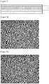
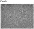
Figure 2 is images photographed cracks generated on the surface of an experimental specimen. Specifically,Figure 2a is an image photographed the surface of Example 1;Figure 2b is an image photographed the surface of Example 2; andFigure 2c is an image photographed the surface of Comparative Example 1. - Hereinafter, the present application will be described in detail through Examples. However, the scope of protection of the present application is not limited by Examples described below.
- The physical properties of Examples and Comparative Examples below were each evaluated in the following manner.
- <Surface Resistance> After heat treating the conductive transparent film prepared in Examples and Comparative Examples at a temperature condition of 130°C for 1 hour, the surface resistance (Ω/□) of the ITO conductive layer was measured through 4-probe measurement (Loresta EP MCP-T360).
- <Transmittance> After heat treating the conductive transparent film prepared in Examples and Comparative Examples at a temperature condition of 130°C for 1 hour, the transmittance was measured using Hazemeter (HM-150, Murakami Color Research Loboratory) and UV-VIS-NIRSPECTROPHOTOMETER (UV-3600, SHIMADZU).
- A protective film was attached to the conductive transparent film in the film form prepared in Examples and Comparative Examples, and the ITO layer was crystallized by heat treatment. Then, the film was cut into a size of 1 mm x 1 mm to prepare a specimen. When the specimen was placed in a bending state with vernier calipers so that the crystallized ITO layer was located on the inner side and maintained for 30 seconds, the bend length at the time when cracks were generated in the ITO layer was measured.
- In the ITO layer that cracks were generated, the length of 100 µm was regarded as one crack, and the lengths of the entire crack generated in the specimen were combined, and then the combined value was divided by 100 µm. As a result, cracks having different lengths and numbers were quantified.
- A solution containing a condensable organosilane compound (methyltrimethoxysilane) was coated on a transparent PET base material having a thickness of 50 µm and thermally cured to form an undercoating layer having a thickness of 40 nm. An anti-crack buffer layer comprising niobium oxide (NbOx) was deposited on the undercoating layer to a thickness of 1 nm by using a sputtering technique, while targeting niobium (Nb) and supplying a mixed gas of argon and oxygen to the deposition equipment. Similarly, an indium oxide layer comprising SnO2 was formed to a thickness of 21.3 nm on the anti-crack buffer layer using the sputtering technique to prepare a conductive transparent film. The constitution and physical properties of the prepared film are as shown in Tables 1 and 2, respectively.
- As shown in the following Table 1, a film was prepared in the same manner as in Example 1, except for the thickness of the anti-crack buffer layer and the surface resistance value. The physical properties of the prepared film are as shown in Table 2.
- As shown in Table 1 below, a film was prepared in the same manner as in Example 1, except that the ITO layer was directly formed on the undercoating layer, without preparing the anti-crack buffer layer. The physical properties of the prepared film are as shown in Table 2.
[Table 1] ITO Thickness (nm) Composition of Anti-crack Buffer Layer Thickness of Anti-crack Buffer Layer (nm) Example 1 21.3 NbO1.5 1 Example 2 21.3 NbO1.5 1.5 Example 3 21.3 NbO1.5 2 Example 4 21.3 NbO1.5 3 Example 5 21.3 NbO1.5 5 Comparative Example 1 21.3 - - [Table 2] Surface Resistance Value (Ω/□) Optical Property Mechanical Property Transmittance (%) Bend Length at the Time of Crack Occurrence (nm) Crack Density (number/mm2) Example 1 92 91.6 16 31.8 Example 2 94 91.2 16 48.6 Example 3 93 90.8 16 46.9 Example 4 94 90.5 16 77.2 Example 5 93 89.8 17 12.4 Comparative Example 1 98 91.6 16 84.3
Claims (15)
- A conductive transparent film comprising a conductive layer; an undercoating layer; and an anti-crack buffer layer.
- The conductive transparent film according to claim 1, wherein said anti-crack buffer layer is positioned between the conductive layer and the undercoating layer.
- The conductive transparent film according to claim 2, wherein said anti-crack buffer layer comprises a metal oxide.
- The conductive transparent film according to claim 3, wherein said metal oxide is NbOx (1≤X≤2.5).
- The conductive transparent film according to claim 3, wherein said anti-crack buffer layer has a thickness of 0.1 nm to 20 nm.
- The conductive transparent film according to claim 1, wherein said conductive layer comprises a transparent conductive oxide.
- The conductive transparent film according to claim 6, wherein said conductive layer has a thickness of 100 nm or less.
- The conductive transparent film according to claim 6, wherein said conductive layer has a surface resistance value in a range of 20 Ω/□ to 300 Ω/□.
- The conductive transparent film according to claim 7, wherein said conductive layer has a surface resistance value in a range of 20 Ω/□ to 95 Ω/□.
- The conductive transparent film according to claim 1, wherein said undercoating layer comprises an organic substance, and said organic substance comprises at least one selected from an acrylic resin, a urethane resin, a thiourethane resin, a melamine resin, an alkyd resin, a siloxane polymer and an organosilane compound represented by Formula 2 below:
[Formula 2] (R1)m-Si-X(4-m)
in Formula 2 above, R1 may be the same or different from each other and is alkyl having 1 to 12 carbon atoms, alkenyl, alkynyl, aryl, arylalkyl, alkylaryl, arylalkenyl, alkenylaryl, arylalkynyl, alkynylaryl, halogen, substituted amino, amide, aldehyde, keto, alkylcarbonyl, carboxy, mercapto, cyano, hydroxy, alkoxy having 1 to 12 carbon atoms, alkoxycarbonyl having 1 to 12 carbon atoms, sulfonic acid, phosphoric acid, acryloxy, methacryloxy, epoxy or a vinyl group, X may be the same or different from each other and is hydrogen, halogen, alkoxy having 1 to 12 carbon atoms, acyloxy, alkylcarbonyl, alkoxycarbonyl, or -N(R2)2 (where R2 is H, or alkyl having 1 to 12 carbon atoms), where oxygen or -NR2 (where R2 is H, or alkyl having 1 to 12 carbon atoms) may also be inserted between a radical R1 and Si to form (R1)m-O-Si-X(4-m) or (R1)m-NR2-Si-X(4-m), and m is an integer of 1 to 3. - The conductive transparent film according to claim 10, wherein said undercoating layer has a thickness of 150 nm or less.
- The conductive transparent film according to claim 1, having a light transmittance of 75% or more.
- The conductive transparent film according to claim 1, wherein after bending said conductive transparent film having a size of 1 mm x 1 mm with vernier calipers, a value of crack density is 80 cracks/mm2 or less, which is measured by dividing the combined length value of the entire crack generated in the conductive layer by 100 µm.
- A method for manufacturing the conductive transparent film according to any one of claims 1 to 13,
comprising a step of sequentially providing an anti-crack buffer layer and a conductive layer on an undercoating layer. - A touch panel comprising the conductive transparent film according to any one of claims 1 to 13.
Applications Claiming Priority (3)
| Application Number | Priority Date | Filing Date | Title |
|---|---|---|---|
| KR20160056329 | 2016-05-09 | ||
| KR1020170056216A KR102159491B1 (en) | 2016-05-09 | 2017-05-02 | A conductive transparent film |
| PCT/KR2017/004751 WO2017196034A1 (en) | 2016-05-09 | 2017-05-08 | Conductive light-transmissive film |
Publications (3)
| Publication Number | Publication Date |
|---|---|
| EP3355317A1 true EP3355317A1 (en) | 2018-08-01 |
| EP3355317A4 EP3355317A4 (en) | 2019-01-02 |
| EP3355317B1 EP3355317B1 (en) | 2022-09-28 |
Family
ID=60808487
Family Applications (1)
| Application Number | Title | Priority Date | Filing Date |
|---|---|---|---|
| EP17796334.5A Active EP3355317B1 (en) | 2016-05-09 | 2017-05-08 | Conductive light-transmissive film |
Country Status (6)
| Country | Link |
|---|---|
| US (1) | US10629327B2 (en) |
| EP (1) | EP3355317B1 (en) |
| JP (1) | JP6762361B2 (en) |
| KR (1) | KR102159491B1 (en) |
| CN (1) | CN108292541B (en) |
| TW (1) | TWI659855B (en) |
Families Citing this family (2)
| Publication number | Priority date | Publication date | Assignee | Title |
|---|---|---|---|---|
| JP7116994B2 (en) * | 2018-06-27 | 2022-08-12 | ロック技研工業株式会社 | ITO film and transparent conductive film |
| CN117985948A (en) * | 2024-02-02 | 2024-05-07 | 湖南旗滨光能科技有限公司 | TCO conductive glass and preparation method and application thereof |
Family Cites Families (18)
| Publication number | Priority date | Publication date | Assignee | Title |
|---|---|---|---|---|
| US6787253B2 (en) * | 2001-06-27 | 2004-09-07 | Bridgestone Corporation | Transparent electroconductive film and touch panel |
| US6896981B2 (en) * | 2001-07-24 | 2005-05-24 | Bridgestone Corporation | Transparent conductive film and touch panel |
| CN201156444Y (en) * | 2008-01-02 | 2008-11-26 | 甘国工 | Flexible high-resistance multi-layered transparent conductive film |
| KR20090121186A (en) | 2008-05-20 | 2009-11-25 | 주식회사 동진쎄미켐 | Substrate manufacturing method and substrate manufactured thereby |
| US8080141B2 (en) | 2008-11-18 | 2011-12-20 | Guardian Industries Corp. | ITO-coated article and/or method of making the same via heat treating |
| TW201129831A (en) * | 2010-02-26 | 2011-09-01 | Ushine Photonics Corp | Transparent conductive laminate comprising visual light adjustment layers |
| KR101669928B1 (en) * | 2010-03-23 | 2016-10-27 | 엘지디스플레이 주식회사 | Flexible flat panel display device |
| JP5691331B2 (en) * | 2010-09-15 | 2015-04-01 | 凸版印刷株式会社 | Method for producing transparent conductive laminate |
| JP5473990B2 (en) * | 2011-06-17 | 2014-04-16 | 日東電工株式会社 | A conductive laminate, a transparent conductive laminate with a patterned wiring, and an optical device. |
| KR20130141746A (en) * | 2012-06-18 | 2013-12-27 | (주)엘지하우시스 | Bending resistance transparent conductive film having bending resistance and the method for manufacturing the same |
| KR101525286B1 (en) * | 2012-09-03 | 2015-06-02 | (주)엘지하우시스 | Coating composition for high refractive layer and transparent conductive film including the same |
| KR20140147420A (en) * | 2013-06-19 | 2014-12-30 | 주식회사 엘지화학 | Method for film substrate coated with transparent conductive materials on both sides |
| CN106164711A (en) * | 2014-04-04 | 2016-11-23 | 乐金华奥斯有限公司 | Low refractive composition and preparation method thereof and nesa coating |
| JP5932097B2 (en) * | 2014-04-17 | 2016-06-08 | 日東電工株式会社 | Transparent conductive film |
| JP6211557B2 (en) * | 2014-04-30 | 2017-10-11 | 日東電工株式会社 | Transparent conductive film and method for producing the same |
| KR20160038623A (en) * | 2014-09-30 | 2016-04-07 | 주식회사 엘지화학 | Transparent conductive film |
| KR20160038624A (en) * | 2014-09-30 | 2016-04-07 | 주식회사 엘지화학 | Transparent conductive film |
| CN104451610B (en) * | 2014-11-24 | 2016-09-07 | 辽宁大学 | The preparation method of Fluorin doped transparent conductive tin oxide thin films |
-
2017
- 2017-05-02 KR KR1020170056216A patent/KR102159491B1/en active Active
- 2017-05-08 US US15/771,628 patent/US10629327B2/en active Active
- 2017-05-08 JP JP2018521611A patent/JP6762361B2/en active Active
- 2017-05-08 TW TW106115149A patent/TWI659855B/en active
- 2017-05-08 CN CN201780004141.2A patent/CN108292541B/en active Active
- 2017-05-08 EP EP17796334.5A patent/EP3355317B1/en active Active
Also Published As
| Publication number | Publication date |
|---|---|
| CN108292541B (en) | 2020-11-17 |
| TWI659855B (en) | 2019-05-21 |
| JP2018535122A (en) | 2018-11-29 |
| EP3355317A4 (en) | 2019-01-02 |
| KR102159491B1 (en) | 2020-09-24 |
| JP6762361B2 (en) | 2020-09-30 |
| TW201801907A (en) | 2018-01-16 |
| EP3355317B1 (en) | 2022-09-28 |
| US10629327B2 (en) | 2020-04-21 |
| US20180322984A1 (en) | 2018-11-08 |
| KR20170126403A (en) | 2017-11-17 |
| CN108292541A (en) | 2018-07-17 |
Similar Documents
| Publication | Publication Date | Title |
|---|---|---|
| TWI570600B (en) | Transparent conductor and touch panel | |
| KR20110125370A (en) | Transparent conductive film of multi-layer structure and manufacturing method thereof | |
| WO2015088938A1 (en) | Transparent conductive multilayer assembly | |
| CN105636775B (en) | Barrier film and method for preparing the same | |
| EP3355317B1 (en) | Conductive light-transmissive film | |
| CN104718582B (en) | Laminated film, film roll thereof, translucent conductive film obtained therefrom, and touch panel using same | |
| CN106527792B (en) | Display panel and display device | |
| JP7238767B2 (en) | Transparent conductive gas barrier laminate and device comprising the same | |
| CN105590662B (en) | Transparent conductor and touch screen | |
| TWI783994B (en) | Transparent conductive film and image display device | |
| JP7287069B2 (en) | Transparent conductive gas barrier laminate, manufacturing method thereof, and device | |
| CN112912540B (en) | barrier film | |
| CN112888730B (en) | Barrier film | |
| KR101640615B1 (en) | Method for preparing transparent conductive film | |
| CN105636774B (en) | Barrier film and method for producing same | |
| KR101371867B1 (en) | Transparent conductive film having excellent optical properties and method for producing the same | |
| KR20160038623A (en) | Transparent conductive film | |
| WO2017196034A1 (en) | Conductive light-transmissive film | |
| KR20160038624A (en) | Transparent conductive film | |
| KR102294026B1 (en) | A barrier film | |
| TWI739184B (en) | Barrier film, electrical element and electronic element | |
| KR20140147420A (en) | Method for film substrate coated with transparent conductive materials on both sides | |
| KR102089409B1 (en) | Barrier film | |
| KR20170126221A (en) | Transparent Conductive Film and Method for Preparing the Same |
Legal Events
| Date | Code | Title | Description |
|---|---|---|---|
| STAA | Information on the status of an ep patent application or granted ep patent |
Free format text: STATUS: THE INTERNATIONAL PUBLICATION HAS BEEN MADE |
|
| PUAI | Public reference made under article 153(3) epc to a published international application that has entered the european phase |
Free format text: ORIGINAL CODE: 0009012 |
|
| STAA | Information on the status of an ep patent application or granted ep patent |
Free format text: STATUS: REQUEST FOR EXAMINATION WAS MADE |
|
| 17P | Request for examination filed |
Effective date: 20180423 |
|
| AK | Designated contracting states |
Kind code of ref document: A1 Designated state(s): AL AT BE BG CH CY CZ DE DK EE ES FI FR GB GR HR HU IE IS IT LI LT LU LV MC MK MT NL NO PL PT RO RS SE SI SK SM TR |
|
| AX | Request for extension of the european patent |
Extension state: BA ME |
|
| RIC1 | Information provided on ipc code assigned before grant |
Ipc: H05K 3/02 20060101ALN20181123BHEP Ipc: B32B 7/00 20060101ALI20181123BHEP Ipc: H01B 1/02 20060101ALI20181123BHEP Ipc: C23C 14/00 20060101ALI20181123BHEP Ipc: H05K 3/38 20060101ALI20181123BHEP Ipc: C09D 201/00 20060101ALI20181123BHEP Ipc: H01B 5/14 20060101AFI20181123BHEP |
|
| A4 | Supplementary search report drawn up and despatched |
Effective date: 20181129 |
|
| DAV | Request for validation of the european patent (deleted) | ||
| DAX | Request for extension of the european patent (deleted) | ||
| STAA | Information on the status of an ep patent application or granted ep patent |
Free format text: STATUS: EXAMINATION IS IN PROGRESS |
|
| 17Q | First examination report despatched |
Effective date: 20201223 |
|
| GRAP | Despatch of communication of intention to grant a patent |
Free format text: ORIGINAL CODE: EPIDOSNIGR1 |
|
| STAA | Information on the status of an ep patent application or granted ep patent |
Free format text: STATUS: GRANT OF PATENT IS INTENDED |
|
| RIC1 | Information provided on ipc code assigned before grant |
Ipc: H05K 3/02 20060101ALN20220705BHEP Ipc: C23C 14/00 20060101ALI20220705BHEP Ipc: H05K 3/38 20060101ALI20220705BHEP Ipc: B32B 7/00 20060101ALI20220705BHEP Ipc: C09D 201/00 20060101ALI20220705BHEP Ipc: H01B 1/02 20060101ALI20220705BHEP Ipc: H01B 5/14 20060101AFI20220705BHEP |
|
| INTG | Intention to grant announced |
Effective date: 20220721 |
|
| RIC1 | Information provided on ipc code assigned before grant |
Ipc: H05K 3/02 20060101ALN20220708BHEP Ipc: C23C 14/00 20060101ALI20220708BHEP Ipc: H05K 3/38 20060101ALI20220708BHEP Ipc: B32B 7/00 20060101ALI20220708BHEP Ipc: C09D 201/00 20060101ALI20220708BHEP Ipc: H01B 1/02 20060101ALI20220708BHEP Ipc: H01B 5/14 20060101AFI20220708BHEP |
|
| GRAS | Grant fee paid |
Free format text: ORIGINAL CODE: EPIDOSNIGR3 |
|
| GRAA | (expected) grant |
Free format text: ORIGINAL CODE: 0009210 |
|
| STAA | Information on the status of an ep patent application or granted ep patent |
Free format text: STATUS: THE PATENT HAS BEEN GRANTED |
|
| AK | Designated contracting states |
Kind code of ref document: B1 Designated state(s): AL AT BE BG CH CY CZ DE DK EE ES FI FR GB GR HR HU IE IS IT LI LT LU LV MC MK MT NL NO PL PT RO RS SE SI SK SM TR |
|
| REG | Reference to a national code |
Ref country code: GB Ref legal event code: FG4D |
|
| REG | Reference to a national code |
Ref country code: CH Ref legal event code: EP |
|
| REG | Reference to a national code |
Ref country code: DE Ref legal event code: R096 Ref document number: 602017062189 Country of ref document: DE |
|
| REG | Reference to a national code |
Ref country code: AT Ref legal event code: REF Ref document number: 1521780 Country of ref document: AT Kind code of ref document: T Effective date: 20221015 |
|
| REG | Reference to a national code |
Ref country code: IE Ref legal event code: FG4D |
|
| REG | Reference to a national code |
Ref country code: LT Ref legal event code: MG9D |
|
| PG25 | Lapsed in a contracting state [announced via postgrant information from national office to epo] |
Ref country code: SE Free format text: LAPSE BECAUSE OF FAILURE TO SUBMIT A TRANSLATION OF THE DESCRIPTION OR TO PAY THE FEE WITHIN THE PRESCRIBED TIME-LIMIT Effective date: 20220928 Ref country code: RS Free format text: LAPSE BECAUSE OF FAILURE TO SUBMIT A TRANSLATION OF THE DESCRIPTION OR TO PAY THE FEE WITHIN THE PRESCRIBED TIME-LIMIT Effective date: 20220928 Ref country code: NO Free format text: LAPSE BECAUSE OF FAILURE TO SUBMIT A TRANSLATION OF THE DESCRIPTION OR TO PAY THE FEE WITHIN THE PRESCRIBED TIME-LIMIT Effective date: 20221228 Ref country code: LV Free format text: LAPSE BECAUSE OF FAILURE TO SUBMIT A TRANSLATION OF THE DESCRIPTION OR TO PAY THE FEE WITHIN THE PRESCRIBED TIME-LIMIT Effective date: 20220928 Ref country code: LT Free format text: LAPSE BECAUSE OF FAILURE TO SUBMIT A TRANSLATION OF THE DESCRIPTION OR TO PAY THE FEE WITHIN THE PRESCRIBED TIME-LIMIT Effective date: 20220928 Ref country code: FI Free format text: LAPSE BECAUSE OF FAILURE TO SUBMIT A TRANSLATION OF THE DESCRIPTION OR TO PAY THE FEE WITHIN THE PRESCRIBED TIME-LIMIT Effective date: 20220928 |
|
| REG | Reference to a national code |
Ref country code: NL Ref legal event code: MP Effective date: 20220928 |
|
| REG | Reference to a national code |
Ref country code: AT Ref legal event code: MK05 Ref document number: 1521780 Country of ref document: AT Kind code of ref document: T Effective date: 20220928 |
|
| PG25 | Lapsed in a contracting state [announced via postgrant information from national office to epo] |
Ref country code: HR Free format text: LAPSE BECAUSE OF FAILURE TO SUBMIT A TRANSLATION OF THE DESCRIPTION OR TO PAY THE FEE WITHIN THE PRESCRIBED TIME-LIMIT Effective date: 20220928 Ref country code: GR Free format text: LAPSE BECAUSE OF FAILURE TO SUBMIT A TRANSLATION OF THE DESCRIPTION OR TO PAY THE FEE WITHIN THE PRESCRIBED TIME-LIMIT Effective date: 20221229 |
|
| PG25 | Lapsed in a contracting state [announced via postgrant information from national office to epo] |
Ref country code: SM Free format text: LAPSE BECAUSE OF FAILURE TO SUBMIT A TRANSLATION OF THE DESCRIPTION OR TO PAY THE FEE WITHIN THE PRESCRIBED TIME-LIMIT Effective date: 20220928 Ref country code: RO Free format text: LAPSE BECAUSE OF FAILURE TO SUBMIT A TRANSLATION OF THE DESCRIPTION OR TO PAY THE FEE WITHIN THE PRESCRIBED TIME-LIMIT Effective date: 20220928 Ref country code: PT Free format text: LAPSE BECAUSE OF FAILURE TO SUBMIT A TRANSLATION OF THE DESCRIPTION OR TO PAY THE FEE WITHIN THE PRESCRIBED TIME-LIMIT Effective date: 20230130 Ref country code: ES Free format text: LAPSE BECAUSE OF FAILURE TO SUBMIT A TRANSLATION OF THE DESCRIPTION OR TO PAY THE FEE WITHIN THE PRESCRIBED TIME-LIMIT Effective date: 20220928 Ref country code: CZ Free format text: LAPSE BECAUSE OF FAILURE TO SUBMIT A TRANSLATION OF THE DESCRIPTION OR TO PAY THE FEE WITHIN THE PRESCRIBED TIME-LIMIT Effective date: 20220928 Ref country code: AT Free format text: LAPSE BECAUSE OF FAILURE TO SUBMIT A TRANSLATION OF THE DESCRIPTION OR TO PAY THE FEE WITHIN THE PRESCRIBED TIME-LIMIT Effective date: 20220928 |
|
| PG25 | Lapsed in a contracting state [announced via postgrant information from national office to epo] |
Ref country code: SK Free format text: LAPSE BECAUSE OF FAILURE TO SUBMIT A TRANSLATION OF THE DESCRIPTION OR TO PAY THE FEE WITHIN THE PRESCRIBED TIME-LIMIT Effective date: 20220928 Ref country code: PL Free format text: LAPSE BECAUSE OF FAILURE TO SUBMIT A TRANSLATION OF THE DESCRIPTION OR TO PAY THE FEE WITHIN THE PRESCRIBED TIME-LIMIT Effective date: 20220928 Ref country code: IS Free format text: LAPSE BECAUSE OF FAILURE TO SUBMIT A TRANSLATION OF THE DESCRIPTION OR TO PAY THE FEE WITHIN THE PRESCRIBED TIME-LIMIT Effective date: 20230128 Ref country code: EE Free format text: LAPSE BECAUSE OF FAILURE TO SUBMIT A TRANSLATION OF THE DESCRIPTION OR TO PAY THE FEE WITHIN THE PRESCRIBED TIME-LIMIT Effective date: 20220928 |
|
| REG | Reference to a national code |
Ref country code: DE Ref legal event code: R097 Ref document number: 602017062189 Country of ref document: DE |
|
| PG25 | Lapsed in a contracting state [announced via postgrant information from national office to epo] |
Ref country code: NL Free format text: LAPSE BECAUSE OF FAILURE TO SUBMIT A TRANSLATION OF THE DESCRIPTION OR TO PAY THE FEE WITHIN THE PRESCRIBED TIME-LIMIT Effective date: 20220928 Ref country code: AL Free format text: LAPSE BECAUSE OF FAILURE TO SUBMIT A TRANSLATION OF THE DESCRIPTION OR TO PAY THE FEE WITHIN THE PRESCRIBED TIME-LIMIT Effective date: 20220928 |
|
| PG25 | Lapsed in a contracting state [announced via postgrant information from national office to epo] |
Ref country code: DK Free format text: LAPSE BECAUSE OF FAILURE TO SUBMIT A TRANSLATION OF THE DESCRIPTION OR TO PAY THE FEE WITHIN THE PRESCRIBED TIME-LIMIT Effective date: 20220928 |
|
| PLBE | No opposition filed within time limit |
Free format text: ORIGINAL CODE: 0009261 |
|
| STAA | Information on the status of an ep patent application or granted ep patent |
Free format text: STATUS: NO OPPOSITION FILED WITHIN TIME LIMIT |
|
| 26N | No opposition filed |
Effective date: 20230629 |
|
| PG25 | Lapsed in a contracting state [announced via postgrant information from national office to epo] |
Ref country code: SI Free format text: LAPSE BECAUSE OF FAILURE TO SUBMIT A TRANSLATION OF THE DESCRIPTION OR TO PAY THE FEE WITHIN THE PRESCRIBED TIME-LIMIT Effective date: 20220928 |
|
| REG | Reference to a national code |
Ref country code: CH Ref legal event code: PL |
|
| PG25 | Lapsed in a contracting state [announced via postgrant information from national office to epo] |
Ref country code: MC Free format text: LAPSE BECAUSE OF FAILURE TO SUBMIT A TRANSLATION OF THE DESCRIPTION OR TO PAY THE FEE WITHIN THE PRESCRIBED TIME-LIMIT Effective date: 20220928 |
|
| REG | Reference to a national code |
Ref country code: BE Ref legal event code: MM Effective date: 20230531 |
|
| PG25 | Lapsed in a contracting state [announced via postgrant information from national office to epo] |
Ref country code: MC Free format text: LAPSE BECAUSE OF FAILURE TO SUBMIT A TRANSLATION OF THE DESCRIPTION OR TO PAY THE FEE WITHIN THE PRESCRIBED TIME-LIMIT Effective date: 20220928 Ref country code: LU Free format text: LAPSE BECAUSE OF NON-PAYMENT OF DUE FEES Effective date: 20230508 Ref country code: LI Free format text: LAPSE BECAUSE OF NON-PAYMENT OF DUE FEES Effective date: 20230531 Ref country code: CH Free format text: LAPSE BECAUSE OF NON-PAYMENT OF DUE FEES Effective date: 20230531 |
|
| REG | Reference to a national code |
Ref country code: IE Ref legal event code: MM4A |
|
| PG25 | Lapsed in a contracting state [announced via postgrant information from national office to epo] |
Ref country code: IE Free format text: LAPSE BECAUSE OF NON-PAYMENT OF DUE FEES Effective date: 20230508 |
|
| PG25 | Lapsed in a contracting state [announced via postgrant information from national office to epo] |
Ref country code: IE Free format text: LAPSE BECAUSE OF NON-PAYMENT OF DUE FEES Effective date: 20230508 |
|
| PG25 | Lapsed in a contracting state [announced via postgrant information from national office to epo] |
Ref country code: IT Free format text: LAPSE BECAUSE OF FAILURE TO SUBMIT A TRANSLATION OF THE DESCRIPTION OR TO PAY THE FEE WITHIN THE PRESCRIBED TIME-LIMIT Effective date: 20220928 Ref country code: BE Free format text: LAPSE BECAUSE OF NON-PAYMENT OF DUE FEES Effective date: 20230531 |
|
| PG25 | Lapsed in a contracting state [announced via postgrant information from national office to epo] |
Ref country code: BG Free format text: LAPSE BECAUSE OF FAILURE TO SUBMIT A TRANSLATION OF THE DESCRIPTION OR TO PAY THE FEE WITHIN THE PRESCRIBED TIME-LIMIT Effective date: 20220928 |
|
| PG25 | Lapsed in a contracting state [announced via postgrant information from national office to epo] |
Ref country code: BG Free format text: LAPSE BECAUSE OF FAILURE TO SUBMIT A TRANSLATION OF THE DESCRIPTION OR TO PAY THE FEE WITHIN THE PRESCRIBED TIME-LIMIT Effective date: 20220928 |
|
| PGFP | Annual fee paid to national office [announced via postgrant information from national office to epo] |
Ref country code: DE Payment date: 20250422 Year of fee payment: 9 |
|
| PGFP | Annual fee paid to national office [announced via postgrant information from national office to epo] |
Ref country code: FR Payment date: 20250422 Year of fee payment: 9 |
|
| PG25 | Lapsed in a contracting state [announced via postgrant information from national office to epo] |
Ref country code: CY Free format text: LAPSE BECAUSE OF FAILURE TO SUBMIT A TRANSLATION OF THE DESCRIPTION OR TO PAY THE FEE WITHIN THE PRESCRIBED TIME-LIMIT; INVALID AB INITIO Effective date: 20170508 |
|
| PG25 | Lapsed in a contracting state [announced via postgrant information from national office to epo] |
Ref country code: HU Free format text: LAPSE BECAUSE OF FAILURE TO SUBMIT A TRANSLATION OF THE DESCRIPTION OR TO PAY THE FEE WITHIN THE PRESCRIBED TIME-LIMIT; INVALID AB INITIO Effective date: 20170508 |
|
| PG25 | Lapsed in a contracting state [announced via postgrant information from national office to epo] |
Ref country code: TR Free format text: LAPSE BECAUSE OF FAILURE TO SUBMIT A TRANSLATION OF THE DESCRIPTION OR TO PAY THE FEE WITHIN THE PRESCRIBED TIME-LIMIT Effective date: 20220928 |
|
| PGFP | Annual fee paid to national office [announced via postgrant information from national office to epo] |
Ref country code: GB Payment date: 20260324 Year of fee payment: 10 |