EP3355198A2 - Runtime address disambiguation in acceleration hardware - Google Patents
Runtime address disambiguation in acceleration hardware Download PDFInfo
- Publication number
- EP3355198A2 EP3355198A2 EP17207172.2A EP17207172A EP3355198A2 EP 3355198 A2 EP3355198 A2 EP 3355198A2 EP 17207172 A EP17207172 A EP 17207172A EP 3355198 A2 EP3355198 A2 EP 3355198A2
- Authority
- EP
- European Patent Office
- Prior art keywords
- memory
- store
- queue
- data
- address
- Prior art date
- Legal status (The legal status is an assumption and is not a legal conclusion. Google has not performed a legal analysis and makes no representation as to the accuracy of the status listed.)
- Withdrawn
Links
Images














Classifications
-
- G—PHYSICS
- G06—COMPUTING OR CALCULATING; COUNTING
- G06F—ELECTRIC DIGITAL DATA PROCESSING
- G06F3/00—Input arrangements for transferring data to be processed into a form capable of being handled by the computer; Output arrangements for transferring data from processing unit to output unit, e.g. interface arrangements
- G06F3/06—Digital input from, or digital output to, record carriers, e.g. RAID, emulated record carriers or networked record carriers
- G06F3/0601—Interfaces specially adapted for storage systems
- G06F3/0602—Interfaces specially adapted for storage systems specifically adapted to achieve a particular effect
- G06F3/0614—Improving the reliability of storage systems
- G06F3/0619—Improving the reliability of storage systems in relation to data integrity, e.g. data losses, bit errors
-
- G—PHYSICS
- G06—COMPUTING OR CALCULATING; COUNTING
- G06F—ELECTRIC DIGITAL DATA PROCESSING
- G06F12/00—Accessing, addressing or allocating within memory systems or architectures
-
- G—PHYSICS
- G06—COMPUTING OR CALCULATING; COUNTING
- G06F—ELECTRIC DIGITAL DATA PROCESSING
- G06F13/00—Interconnection of, or transfer of information or other signals between, memories, input/output devices or central processing units
- G06F13/14—Handling requests for interconnection or transfer
- G06F13/16—Handling requests for interconnection or transfer for access to memory bus
-
- G—PHYSICS
- G06—COMPUTING OR CALCULATING; COUNTING
- G06F—ELECTRIC DIGITAL DATA PROCESSING
- G06F3/00—Input arrangements for transferring data to be processed into a form capable of being handled by the computer; Output arrangements for transferring data from processing unit to output unit, e.g. interface arrangements
- G06F3/06—Digital input from, or digital output to, record carriers, e.g. RAID, emulated record carriers or networked record carriers
- G06F3/0601—Interfaces specially adapted for storage systems
- G06F3/0628—Interfaces specially adapted for storage systems making use of a particular technique
- G06F3/0646—Horizontal data movement in storage systems, i.e. moving data in between storage devices or systems
- G06F3/065—Replication mechanisms
-
- G—PHYSICS
- G06—COMPUTING OR CALCULATING; COUNTING
- G06F—ELECTRIC DIGITAL DATA PROCESSING
- G06F3/00—Input arrangements for transferring data to be processed into a form capable of being handled by the computer; Output arrangements for transferring data from processing unit to output unit, e.g. interface arrangements
- G06F3/06—Digital input from, or digital output to, record carriers, e.g. RAID, emulated record carriers or networked record carriers
- G06F3/0601—Interfaces specially adapted for storage systems
- G06F3/0668—Interfaces specially adapted for storage systems adopting a particular infrastructure
- G06F3/067—Distributed or networked storage systems, e.g. storage area networks [SAN], network attached storage [NAS]
-
- G—PHYSICS
- G06—COMPUTING OR CALCULATING; COUNTING
- G06F—ELECTRIC DIGITAL DATA PROCESSING
- G06F9/00—Arrangements for program control, e.g. control units
- G06F9/06—Arrangements for program control, e.g. control units using stored programs, i.e. using an internal store of processing equipment to receive or retain programs
- G06F9/30—Arrangements for executing machine instructions, e.g. instruction decode
- G06F9/30003—Arrangements for executing specific machine instructions
- G06F9/3004—Arrangements for executing specific machine instructions to perform operations on memory
- G06F9/30043—LOAD or STORE instructions; Clear instruction
-
- G—PHYSICS
- G06—COMPUTING OR CALCULATING; COUNTING
- G06F—ELECTRIC DIGITAL DATA PROCESSING
- G06F9/00—Arrangements for program control, e.g. control units
- G06F9/06—Arrangements for program control, e.g. control units using stored programs, i.e. using an internal store of processing equipment to receive or retain programs
- G06F9/30—Arrangements for executing machine instructions, e.g. instruction decode
- G06F9/38—Concurrent instruction execution, e.g. pipeline or look ahead
- G06F9/3824—Operand accessing
- G06F9/3826—Bypassing or forwarding of data results, e.g. locally between pipeline stages or within a pipeline stage
-
- G—PHYSICS
- G06—COMPUTING OR CALCULATING; COUNTING
- G06F—ELECTRIC DIGITAL DATA PROCESSING
- G06F9/00—Arrangements for program control, e.g. control units
- G06F9/06—Arrangements for program control, e.g. control units using stored programs, i.e. using an internal store of processing equipment to receive or retain programs
- G06F9/30—Arrangements for executing machine instructions, e.g. instruction decode
- G06F9/38—Concurrent instruction execution, e.g. pipeline or look ahead
- G06F9/3824—Operand accessing
- G06F9/3834—Maintaining memory consistency
Definitions
- the present disclosure relates to the acceleration hardware, and in particular, to runtime address disambiguation in acceleration hardware such as spatial arrays.
- Acceleration hardware refers to devices that speed up data communications, storage and retrieval, encryption and decryption, mathematical operations, graphics, Web page viewing, and the like. Acceleration hardware may include individual integrated circuit (also called an IC or chip), a printed circuit card, or a self-contained system. A few examples of acceleration hardware include a network access accelerator (NAS), a graphics accelerator, and a floating point accelerator (FPA). In one embodiment, acceleration hardware is instantiated as spatial architecture, which is energy efficient and a high-performance means of accelerating user applications in computing systems using spatial arrays.
- a spatial architecture includes an array of processing components, such as gates in a Field Programmable Gate Array (FPGA) or other processing elements (PE).
- FPGA Field Programmable Gate Array
- PE processing elements
- spatial fabric such as exists in a Field Programmable Gate Array (FPGA), in a Loop-Processing Unit (LPU), or the like.
- FPGA Field Programmable Gate Array
- LPU Loop-Processing Unit
- a challenge faced by such architectures is the mapping of a broad set of existing sequential or partially parallel applications to the spatial array, which is distributed by nature and highly parallel.
- the main difficultly in performing this mapping is the automatic parallelization of memory accesses in legacy programs due to a centralized, largely sequential memory model present in legacy programming environments.
- compilers cannot prove that f(i) is not the same as g(i), either for the same value of i or different values of i across loop bodies. This is known as pointer or memory aliasing.
- compilers are usually forced to serialize the accesses to the array, p. However, it is often the case at runtime that f(i) and g(i) are not equal, giving an opportunity to obtain dynamic parallelism in hardware. In spatial architectures, however, no mechanisms exist to check for and exploit dependencies that facilitate exploiting parallelism that may arise during code execution.
- the disclosed architecture provides flexibility and parallelism within runtime microarchitecture, while preserving memory semantics of an original sequential program, including preservation of dependencies between memory operations that should occur in a certain order.
- the disclosed microarchitecture for example, enables parallelization and acceleration of legacy sequential codes within acceleration hardware, facilitating the acceleration of software applications.
- an integrated circuit includes memory ordering circuitry coupled to a memory subsystem and to acceleration hardware, which may include a patchwork of processing components.
- a processor executing corresponding instructions may request memory operations to the memory subsystem out of program order.
- the memory ordering circuitry of the disclosed architecture may ensure that, as the acceleration hardware executes a sub-program corresponding to instructions of a program, results of corresponding memory operations are ordered in sequential order of the program.
- the memory ordering circuitry may include a directed logical channel formed between predecessor and successor memory operations, and a dependency token may be passed in association with an address within this channel to indicate dependency to a subsequent memory operation.
- a directed logical channel may be referred to as queue herein, which may be implemented with various hardware structures as will be explained. The location within this logical channel and of an associated dependency token may be tracked, depending on operation type, using memory arguments within queued memory operations.
- the memory ordering circuitry may queue the memory operations in an operations queue.
- the memory ordering circuitry may also receive, from the acceleration hardware in an input queue, addresses in whatever order the acceleration hardware executes and delivers the addresses for the memory operations. For example, for a load operation, a load address queue may receive an address from which to retrieve data from the memory. Similarly, for a store operation, a store address queue may receive an address to which to write data to the memory, and a store data queue to buffer data to be written to that address.
- store operations may be performed in two phases: first to schedule a store operation to a particular address, and second, to request the store operation upon receipt of the data to be stored.
- disclosed architecturally-defined memory operations may be capable of honoring memory ordering constraints through the manipulation of dependency tokens.
- Use of dependency tokens may ensure retention of data dependency of a memory operation within a program with a preceding memory operation.
- a memory operation may trigger generation of a dependency token upon the result of the operation becoming available to other memory operations. This generation may include the option of passing on a dependency token received from a preceding memory operation, such as duplication of that dependency token.
- These tokens are then passed to program-subsequent memory operations in a spatial execution graph representing the program.
- the subsequent operation is enabled for scheduling.
- a counter may be used to track how many dependency tokens have been generated for any given channel, e.g., providing a compact representation of a queue.
- the ordering of memory operations produced by a compiler, or the program memory graph (or hand-assembled code) ensures that program memory order is honored within parallel-executing acceleration hardware such as spatial fabric.
- a dependency token may be scheduled and ultimately executed in program order.
- a dependency exists between a store operation and a preceding load operation when the store is to the same address in memory as the load operation.
- a dependency token may be generated (or duplicated) to be passed with the load operation, so that ordering circuitry may schedule completion of the load operation (that carries the dependency token) before that of the store operation. Ordering the store operation before the load operation in this example may avoid the scenario in which the store operation eliminates existing data before the load operation has a chance to read the existing data.
- a dependency may exist between a load operation and a prior store operation to the same address in memory.
- load-load and store-store dependencies may also exist for which dependency tokens may facilitate in-order scheduling and completion of serial load operations or serial store operations, respectively.
- the disclosed microarchitecture may include a memory interface coupled to a memory subsystem, which includes a memory to store data corresponding to instructions being executed for a program.
- the microarchitecture may also include an operations queue to buffer memory operations corresponding to the instructions, and a acceleration hardware of processing components that are to execute the sub-program corresponding to the instructions.
- the microarchitecture may also include a set of input queues coupled to the acceleration hardware, including a store address queue, a store data queue, a load address queue, and associated dependency queues or counters.
- the store address queue may receive, from the acceleration hardware, a store address of the memory that is associated with a store operation.
- the store data queue may receive, from the acceleration hardware, data to be stored at the store address of the memory.
- the microarchitecture may also include a completion queue to buffer response data for load operations, and a load address queue in which to receive a load address for a load operation.
- a load response When a load response is received from the memory, data of the load response may be stored in an in-order next slot of the completion queue, which may then be sent out to the acceleration hardware with any dependency token.
- the microarchitecture may further include a disambiguator circuit that may provide a means by which the microarchitecture may check for address conflicts as early as possible during scheduling of memory operations, even before data is available for those memory operations.
- the disambiguator circuit may store prior program-order memory accesses in a disambiguator queue, which may be queried for the presence of a particular address.
- the disambiguator circuit may be implemented, for example, as a content-address memory (CAM) or a counting Bloom filter, which will be discussed in more detail.
- CAM content-address memory
- a scheduler circuit may query, in program order and on behalf of a succeeding memory operation, the disambiguator circuit to determine whether there exists an address conflict with that succeeding memory operation.
- a succeeding memory operation is one that semantically follows and a preceding memory operation is one that semantically comes before.
- This early checking of address conflicts may improve both memory latency and throughput, as memory operations can be issued in parallel (provided no address conflict) and without suffering the latency of serialized memory access.
- the scheduler circuit may query the disambiguator circuit to determine whether the load address matches the store address. The disambiguator circuit may then, responsive to determining that the load address is not the same as the store address, trigger the scheduler circuit to proceed with issuing the load operation to the memory. In contrast, the disambiguator circuit may, responsive to determining that the load address is the same as the store address, and thus conflicts, copy the data from the store data queue into the completion queue for the load operation, to perform "store forwarding" of the data for the load operation.
- the disambiguator circuit may buffer the data from the store address queue (once received) and thus may directly forward the data to the completion queue.
- the disambiguator circuit may store an entry into the disambiguation queue that includes the store address and a pointer that points to the location at which the store data queue will receive the data.
- the scheduler circuit may mark, with the pointer, the load operation as a store forward, so that the scheduler circuit may perform the data forwarding from the store data queue to the completion queue in response to the store data queue receiving the data.
- the pointer may be a type of second dependency token, which may be associated with an index into the store data queue.
- the scheduler circuit may schedule the succeeding load operation for completion once the store operation has been scheduled, and there is a load address available for the succeeding load operation.
- the scheduler circuit schedules the succeeding load operation by annotating an indexed slot of the completion queue with the location of the pointer into the store data queue.
- the completion queue in this way, knows to retrieve data to complete the load operation from the location in the store data queue.
- the load operation may then complete, without sending a request to memory, once the data arrives in the store data queue and is forwarded to the completion queue.
- This type of store forwarding saves time (in processing cycles), ensures correct program order in issuing memory operations, and therefore, improves both memory latency and throughput.
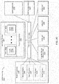
- FIG. 1A is a block diagram of a system 100 that employs a memory ordering circuit 105 interposed between a memory subsystem 110 and acceleration hardware 102, according to an embodiment of the present disclosure.
- the memory subsystem 110 may include known memory components, including cache, memory, and one or more memory controller(s) associated with a processor-based architecture.
- the acceleration hardware 102 may be coarse-grained spatial architecture made up of lightweight processing elements (or other types of processing components) connected by an inter-processing element (PE) network or another type of inter-component network.
- PE inter-processing element
- programs are mapped onto the spatial architecture by configuring PEs and a communications network.
- PEs are configured as dataflow operators, similar to functional units in a processor: once the input operands arrive at the PE, some operation occurs, and results are forwarded to downstream PEs in a pipelined fashion.
- Dataflow operators (or other types of operators) may choose to consume incoming data on a per-operator basis.
- Simple operators like those handling the unconditional evaluation of arithmetic expressions often consume all incoming data. It is sometimes useful, however, for operators to maintain state, for example, in accumulation.
- the PEs communicate using dedicated virtual circuits, which are formed by statically configuring a circuit-switched communications network. These virtual circuits are flow controlled and fully back pressured, such that PEs will stall if either the source has no data or the destination is full.
- data flows through the PEs implementing a mapped algorithm according to a data-flow graph, also referred to as a subprogram herein. For example, data may be streamed in from memory, through the acceleration hardware 102, and then back out to memory.
- a data-flow graph also referred to as a subprogram herein.
- data may be streamed in from memory, through the acceleration hardware 102, and then back out to memory.
- Such an architecture can achieve remarkable performance efficiency relative to traditional multicore processors: compute, in the form of PEs, is simpler and more numerous than larger cores and communication is direct, as opposed to an extension of the memory subsystem 110.
- the disclosed memory ordering circuit 105 includes memory ordering architecture and microarchitecture, as will be explained in detail.
- the memory ordering circuit 105 is a request address file circuit (or "RAF") or other memory request circuitry.
- FIG. 1B is a block diagram of the system 100 of Figure 1A but which employs multiple memory ordering circuits 105, according to an embodiment of the present disclosure.
- Each memory ordering circuit 105 may function as an interface between the memory subsystem 110 and a portion of the acceleration hardware 102.
- the memory subsystem 110 may include a plurality of cache slices 12 (e.g., cache slices 12A, 12B, 12C, and 12D in the embodiment of Figure 1B ), and a certain number of memory ordering circuits 105 (four in this embodiment) may be used for each cache slice 12.
- a crossbar 104 may connect the memory ordering circuits 105 to banks of cache that make up each cache slice 12A, 12B, 12C, and 12D. For example, there may be eight banks of memory in each cache slice in one embodiment.
- the system 100 may be instantiated on a single die, for example, as a system on a chip (SoC).
- SoC includes the acceleration hardware 102.
- the acceleration hardware 102 is an external programmable chip such as an FPGA or CGRA, and the memory ordering circuits 105 interface with the acceleration hardware 102 through an input/output hub or the like.
- Each memory ordering circuit 105 may accept read and write requests to the memory subsystem 110.
- the requests from the acceleration hardware 102 arrive at the memory ordering circuit 105 in a separate channel for each node of the data-flow graph that initiates read or write accesses, also referred to as load or store accesses herein. Buffering is provided so that the processing of loads will return the requested data to the acceleration hardware 102 in the order it was requested. In other words, iteration six data is returned before iteration seven data, and so forth.
- the request channel from a memory ordering circuit 105 to a particular cache bank may be implemented as an ordered channel and any first request that leaves before a second request will arrive at the cache bank before the second request.
- FIG. 2 is a block diagram 200 illustrating general functioning of memory operations into and out of the acceleration hardware 102, according to an embodiment of the present disclosure.
- the operations occurring out the top of the acceleration hardware 102 are understood to be made to and from a memory of the memory subsystem 110. Note that two load requests are made, followed by corresponding load responses. While the acceleration hardware 102 performs processing on data from the load responses, a third load request and response occur, which trigger additional acceleration hardware processing. The results of the acceleration hardware processing for these three load operations are then passed into a store operation, and thus a final result is stored back to memory.
- the acceleration hardware 102 such as spatial fabric, is latency-insensitive in terms of the request and response channels, and inherent parallel processing that may occur.
- the acceleration hardware may also decouple execution of a program from implementation of the memory subsystem 110 ( Figure 1A ), as interfacing with the memory occurs at discrete moments separate from multiple processing steps taken by the acceleration hardware 102.
- a load request to and a load response from memory are separate actions, and may be scheduled differently in different circumstances depending on dependency flow of memory operations.
- the use of spatial fabric, for example, for processing instructions facilitates spatial separation and distribution of such a load request and a load response.
- FIG. 3 is a block diagram 300 illustrating a spatial dependency flow for a store operation 301, according to an embodiment of the present disclosure.
- Reference to a store operation is exemplary, as the same flow may apply to a load operation (but without incoming data), or to other operators such as a fence.
- a fence is an ordering operation for memory subsystems that ensures that all prior memory operations of a type (such as all stores or all loads) have completed.
- the store operation 301 may receive an address 302 (of memory) and data 304 received from the acceleration hardware 102.
- the store operation 301 may also receive an incoming dependency token 308, and in response to the availability of these three items, the store operation 301may generate an outgoing dependency token 312.
- the incoming dependency token which may, for example, be an initial dependency token of a program, may be provided in a compiler-supplied configuration for the program, or may be provided by execution of memory-mapped input/output (I/O).
- the incoming dependency token 308 may be received from the acceleration hardware 102, e.g., in association with a preceding memory operation from which the store operation 301 depends.
- the outgoing dependency token 312 may be generated based on the address 302 and data 304 being required by a program-subsequent memory operation.
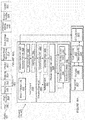
- FIG 4 is a detailed block diagram of the memory ordering circuit 105 of Figure 1A , according to an embodiment of the present disclosure.
- the memory ordering circuit 105 may be coupled to an out-of-order memory subsystem 110, which as discussed, may include cache 12 and memory 18, and associated out-of-order memory controller(s).
- the memory ordering circuit 105 may include, or be coupled to, a communications network interface 20 that may be either an inter-tile or an intra-tile network interface, and may be a circuit switched network interface (as illustrated), and thus include circuit-switched interconnects. Alternatively, or additionally, the communications network interface 20 may include packet-switched interconnects.
- the memory ordering circuit 105 may further include, but not be limited to, a memory interface 410, an operations queue 412, input queue(s) 416, a completion queue 420, an operation configuration data structure 424, an operations manager circuit 430 that may further include a scheduler circuit 432 and an execution circuit 434, and a disambiguator circuit 450 that includes a disambiguator queue 452.
- the memory interface 410 may be circuit-switched, and in another embodiment, the memory interface 410 may be packet-switched, or both may exist simultaneously.
- the operations queue 412 may buffer memory operations (with corresponding arguments) that are being processed for request, and may, therefore, correspond to addresses and data coming into the input queues 416.
- the input queues 416 may be an aggregation of at least the following: a load address queue, a store address queue, a store data queue, and a dependency queue.
- the memory ordering circuit 105 may provide for sharing of logical queues, with additional control logic to logically separate the queues, which are individual channels with the memory ordering circuit. This may maximize input queue usage, but may also require additional complexity and space for the logic circuitry to manage the logical separation of the aggregated queue.
- the input queues 416 may be implemented in a segregated fashion, with a separate hardware queue for each. Whether aggregated ( Figure 4 ) or disaggregated ( Figure 5 ), implementation for purposes of this disclosure is substantially the same, with the former using additional logic to logically separate the queues within a single, shared hardware queue.
- the input queues 416 and the completion queue 420 may be implemented as ring buffers of a fixed size.
- a ring buffer is an efficient implementation of a circular queue that has a first-in-first-out (FIFO) data characteristic. These queues may, therefore, enforce a semantical order of a program for which the memory operations are being requested.
- a ring buffer (such as for the store address queue) may have entries corresponding to entries flowing through an associated queue (such as the store data queue or the dependency queue) at the same rate. In this way, a store address may remain associated with corresponding store data.
- the load address queue may buffer an incoming address of the memory 18 from which to retrieve data.
- the store address queue may buffer an incoming address of the memory 18 to which to write data, which is buffered in the store data queue.
- the dependency queue may buffer dependency tokens in association with the addresses of the load address queue and the store address queue.
- Each queue, representing a separate channel, may be implemented with a fixed or dynamic number of entries. When fixed, the more entries that are available, the more efficient complicated loop processing may be made. But, having too many entries costs more area and energy to implement.
- the disclosed input queue 416 may share queue slots. Use of the slots in a queue may be statically allocated.
- the completion queue 420 may be a separate set of queues to buffer data received from memory in response to memory commands issued by load operations.
- the completion queue 420 may be used to hold a load operation that has been scheduled but for which data has not yet been received (and thus has not yet completed).
- the completion queue 420 may therefore, be used to reorder data and operation flow.
- the operations manager circuit 430 may provide logic for scheduling and executing queued memory operations when taking into account dependency tokens used to provide correct ordering of the memory operations, and entries queued in the disambiguator circuit 450.
- the operation manager circuit 430 may access the operation configuration data structure 424 to determine which queues are grouped together to form a given memory operation.
- the operation configuration data structure 424 may include that a specific dependency counter (or queue), input queue, output queue, and completion queue are all grouped together for a particular memory operation. As each successive memory operation may be assigned a different group of queues, access to varying queues may be interleaved across a sub-program of memory operations.
- the operations manager circuit 430 may interface with the operations queue 412, the input queue(s) 416, the completion queue(s) 420, and the memory subsystem 110 to initially issue memory operations to the memory subsystem 110 when successive memory operations become "executable," and to next complete the memory operation with some acknowledgement from the memory subsystem.
- This acknowledgement may be, for example, data in response to a load operation command or an acknowledgement of data being stored in the memory in response to a store operation command.
- the disambiguator circuit 450 may provide the means by which the operations manager circuit 430 may track store operations, and check whether a succeeding load operation has an address conflict with any pending store operation. To do so, the disambiguator circuit may store entries into the disambiguator queue 452 for store operations, each entry including a store address and a pointer that points to a location in the store data queue associated with the store address. This pointer may be generated by the scheduler circuit 432 annotating an index into the store data queue 452 at that location, e.g., the indexed slot within the store data queue that will receive data to be stored at the store address. Other types of pointers are envisioned depending on the types of queues used.
- the operations manager circuit 430 may then, on behalf of the succeeding load operation, request that the disambiguator circuit 450 perform a search of the disambiguator queue 452 to determine whether a load address matches (e.g., conflicts with) the store address for any of the pending store operation entries in the disambiguator. Accordingly, the disambiguator circuit 450 may perform an early address conflict check, before arrival of associated data. This early checking of address conflicts may improve both memory latency and throughput, as memory operations can be issued in parallel (provided no address conflict) and without incurring the latency of serialized memory access.
- the disambiguator circuit 450 may buffer the data from the store address queue and thus may directly forward the data to the completion queue 420 for the succeeding load operation.
- the operations manager circuit 430 may use the entry in the disambiguator queue 452 (located based on an address match with the load address) to forward data, upon arrival into the store data queue, to the completion queue 420, thus allowing the succeeding load operation. Completion of the load operation may, therefore, occur without sending a load request to the memory subsystem 110, and may significantly improve latency and throughput of handling memory operations in and out of the acceleration hardware 102.
- the operations manager circuit 430 may further trigger generation of a dependency token to indicate, to the succeeding load operation, a dependency on the data being stored by the store operation.
- the operations manager circuit 430 may include the dependency token with the store operation, when scheduled, and be sent with the store operation to memory, e.g., in a store command.
- the disambiguator circuit 450 is a content-addressable memory (CAM) or a counting Bloom filter.
- a CAM is a hardware search engine that is faster than algorithmic approaches for search-intensive applications.
- a CAM may be composed of conventional semiconductor memory (usually SRAM), which may be the disambiguator queue 452 as referred to herein, with added comparison circuitry that enables a search operation to complete in a single clock cycle.
- SRAM semiconductor memory
- Two common search-intensive tasks that use CAMs include packet forwarding and packet classification in routers.
- a CAM may be employed to search for matching memory addresses (e.g., between succeeding loads and pending stores), and provide, to the operations manager circuit 430, metadata information such as the store address and pointer, into an index of the store data queue, associated with the store address.
- the CAM may also buffer data in conjunction with such metadata, which data may be forwarded to succeeding memory operations.
- a Bloom filter is a space-efficient probabilistic data structure that is used to test whether an element is a member of a set. False positive matches are possible, but false negatives are not, and thus the Bloom filter has a 100% recall rate.
- a query returns either "possibly in set” or “definitely not in the set.” Elements may be added to the set, and with a counting Bloom filter, elements may be removed.
- a similar disambiguator queue 452 e.g., SRAM or other type of re-writable memory
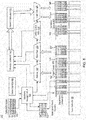
- FIG 5 is a flow diagram of a microarchitecture 500 of the memory ordering circuit 105 of Figure 1A , according to an embodiment of the present disclosure.
- the memory subsystem 110 may allow illegal execution of a program in which ordering of memory operations is wrong, due to the semantics of C language (and other object-oriented program languages).
- the microarchitecture 500 may enforce the ordering of the memory operations (sequences of loads from and stores to memory) so that results of instructions that the acceleration hardware 102 executes are properly ordered.
- a number of local networks 50 are illustrated to represent a portion of the acceleration hardware 102 coupled to the microarchitecture 500.
- the compiler expresses the dependency between the store operation and the load operation to an array, p, in some fashion, which are expressed via dependency tokens as will be explained.
- the microarchitecture 500 finds and issues as many load commands of an array in parallel as is legal with respect to program order.
- the microarchitecture 500 may include the operations queue 412, the input queues 416, the completion queues 420, and the operations manager circuit 430 discussed with reference to Figure 4 , above, where individual queues may be referred to as channels.
- the microarchitecture 500 may further include a plurality of dependency token counters 514 (e.g., one per input queue), a set of dependency queues 518 (e.g., one each per input queue), an address multiplexer 532, a store data multiplexer 534, a completion queue index multiplexer 536, and a load data multiplexer 538.
- the operations manager circuit 430 in one embodiment, may direct these various multiplexers in generating a memory command 550 (to be sent to the memory subsystem 110) and in receipt of responses of load commands back from the memory subsystem 110, as will be explained.
- the input queues 416 may include a load address queue 522, a store address queue 524, and a store data queue 526. (The small numbers 0, 1, 2 are channel labels and will be referred to later in Figure 8 and Figure 14A .) In various embodiments, these input queues may be multiplied to contain additional channels, to handle additional parallelization of memory operation processing.
- Each dependency queue 518 may be associated with one of the input queues 416. More specifically, the dependency queue 518 labeled B0 may be associated with the load address queue 522 and the dependency queue labeled B1 may be associated with the store address queue 524. If additional channels of the input queues 416 are provided, the dependency queues 518 may include additional, corresponding channels.
- the completion queues 420 may include a set of output buffers 544 and 546 for receipt of load data from the memory subsystem 110 and a completion queue 542 to buffer addresses and data for load operations according to an index maintained by the operations manager circuit 430.
- the operations manager circuit 430 can manage the index to ensure in-order execution of the load operations, and to identify data received into the output buffers 544 and 546 that may be moved to scheduled load operations in the completion queue 542.
- the microarchitecture 500 may reorder memory operations with use of the completion queue 542.
- Three different sub-operations may be performed in relation to the completion queue 542, namely to allocate, enqueue, and dequeue.
- the operations manager circuit 430 may allocate an index into the completion queue 542 in an in-order next slot of the completion queue. The operations manager circuit may provide this index to the memory subsystem 110, which may then know the slot to which to write data for a load operation.
- the memory subsystem 110 may write data as an entry to the indexed, in-order next slot in the completion queue 542 like random access memory (RAM), setting a status bit of the entry to valid.
- the operations manager circuit 430 may present the data stored in this in-order next slot to complete the load operation, setting the status bit of the entry to invalid. Invalid entries may then be available for a new allocation.
- the status signals 448 may refer to statuses of the input queues 416, the completion queues 420, the dependency queues 518, and the dependency token counters 514. These statuses, for example, may include an input status, an output status, and a control status, which may refer to the presence or absence of a dependency token in association with an input or an output.
- the input status may include the presence or absence of addresses and the output status may include the presence or absence of store values and available completion buffer slots.
- the dependency token counters 514 may be a compact representation of a queue and track a number of dependency tokens used for any given input queue. If the dependency token counters 514 saturate, no additional dependency tokens may be generated for new memory operations. Accordingly, the memory ordering circuit 105 may stall scheduling new memory operations until the dependency token counters 514 becomes unsaturated.
- Figure 6 is a block diagram of an executable determiner circuit 600, according to an embodiment of the present disclosure.
- the memory ordering circuit 105 may be set up with several different kinds of memory operations, for example a load and a store:
- the executable determiner circuit 600 may be integrated as a part of the scheduler circuit 432 and which may perform a logical operation to determine whether a given memory operation is executable, and thus ready to be issued to memory.
- a memory operation may be executed when the queues corresponding to its memory arguments have data and an associated dependency token is present.
- These memory arguments may include, for example, an input queue identifier 610 (indicative of a channel of the input queue 416), an output queue identifier 620 (indicative of a channel of the completion queues 420), a dependency queue identifier 630 (e.g., what dependency queue or counter should be referenced), an operation type indicator 640 (e.g., load operation or store operation), and a CAM indicator 645 (e.g., whether to query the disambiguator queue 452 for an address conflict for load operations or to store an entry into the disambiguator queue 452 for store operations).
- an input queue identifier 610 indicative of a channel of the input queue 416
- an output queue identifier 620 indicative of a channel of the completion queues 420
- a dependency queue identifier 630 e.g., what dependency queue or counter should be referenced
- an operation type indicator 640 e.g., load operation or store operation
- a CAM indicator 645 e.g.,
- these memory arguments are queued within the operations queue 412, and used to schedule issuance of memory operations in association with incoming addresses and data from memory and the acceleration hardware 102.
- Incoming status signals 448 may be logically combined with these identifiers and then the results may be added (e.g., through an AND gate 650) to output an executable signal, e.g., which is asserted when the memory operation is executable.
- the status signals 448 as inputs, may include an input status 612 for the input queue identifier 610, an output status 622 for the output queue identifier 620, and a control status 632 (related to dependency tokens) for the dependency queue identifier 630.
- the memory ordering circuit 105 may issue a load command when the load operation has an address (input status) and room to buffer the load result in the completion queue 542 (output status). Similarly, the memory ordering circuit 105 may issue a store command for a store operation when the store operation has both an address and data value (input status). Accordingly, the status signals 448 may communicate a level of emptiness (or fullness) of the queues to which the status signals pertain. The operation type may then dictate whether the logic results in an executable signal depending on what address and data should be available.
- the scheduler circuit 432 may extend memory operations to include dependency tokens as underlined above in the example load and store operations.
- the control status 632 may indicate whether a dependency token is available within the dependency queue identified by the dependency queue identifier 630, which could be one of the dependency queues 518 (for an incoming memory operation) or a dependency token counter 514 (for a completed memory operation).
- a dependent memory operation requires an additional ordering token to execute and generates an additional ordering token upon completion of the memory operation, where completion means that data from the result of the memory operation has become available to program-subsequent memory operations.
- the operations manager circuit 430 may direct the address multiplexer 532 to select an address argument that is buffered within either the load address queue 522 or the store address queue 524, depending on whether a load operation or a store operation is currently being scheduled for execution. If it is a store operation, the operations manager circuit 430 may also direct the store data multiplexer 534 to select corresponding data from the store data queue 526. The operations manager circuit 430 may also direct the completion queue index multiplexer 536 to retrieve a load operation entry, indexed according to queue status and/or program order, within the completion queues 420, to complete a load operation.
- the operations manager circuit 430 may also direct the load data multiplexer 538 to select data received from the memory subsystem 110 into the completion queues 420 for a load operation that is awaiting completion. In this way, the operations manager circuit 430 may direct selection of inputs that go into forming the memory command 550, e.g., a load command or a store command, or that the execution circuit 434 is waiting for to complete a memory operation.
- Figure 7 is a block diagram the execution circuit 434 that may include a priority encoder 706 and selection circuitry 708 and which generates output control line(s) 710, according to one embodiment of the present disclosure.
- the execution circuit 434 may access queued memory operations (in the operations queue 412) that have been determined to be executable ( Figure 6 ).
- the execution circuit 434 may also receive the schedules 704A, 704B, 704C for multiple of the queued memory operations that have been queued and also indicated as ready to issue to memory.
- the priority encoder 706 may thus receive an identity of the executable memory operations that have been scheduled and execute certain rules (or follow particular logic) to select the memory operation from those coming in that has priority to be executed first.
- the priority encoder 706 may output a selector signal 707 that identifies the scheduled memory operation that has a highest priority, and has thus been selected.
- the priority encoder 706, may be a circuit (such as a state machine or a simpler converter) that compresses multiple binary inputs into a smaller number of outputs, including possibly just one output.
- the output of a priority encoder is the binary representation of the original number starting from zero of the most significant input bit. So, in one example, when memory operation 0 ("zero"), memory operation one ("1"), and memory operation two (“2") are executable and scheduled, corresponding to 704A, 704B, and 704C, respectively.
- the priority encoder 706 may be configured to output the selector signal 707 to the selection circuitry 708 indicating the memory operation zero as the memory operation that has highest priority.
- the selection circuitry 708 may be a multiplexer in one embodiment, and be configured to output its selection (e.g., of memory operation zero) onto the control lines 710, as a control signal, in response to the selector signal from the priority encoder 706 (and indicative of selection of memory operation of highest priority).
- This control signal may go to the multiplexers 532, 534, 536, and/or 538, as discussed with reference to Figure 5 , to populate the memory command 550 that is next to issue (be sent) to the memory subsystem 110.
- the transmittal of the memory command may be understood to be issuance of a memory operation to the memory subsystem 110.
- FIG 8 is a block diagram of an exemplary load operation 800, both logical and in binary form, according to an embodiment of the present disclosure.
- the logical representation of the load operation 800 may include channel zero ("0") (corresponding to the load address queue 522) as the input queue identifier 610 and completion channel one ("1") (corresponding to the output buffer 544) as the output queue identifier 620.
- the dependency queue identifier 630 may include two identifiers, channel B0 (corresponding to the first of the dependency queues 518) for incoming dependency tokens and counter C0 for outgoing dependency tokens.
- the operation type 640 has an indication of "Load,” which could be a numerical indicator as well, to indicate the memory operation is a load operation.
- the CAM indicator 645 may be a binary "zero” or "one” decision whether to query the disambiguator circuit 450 during scheduling the memory operation.
- Below the logical representation of the logical memory operation is a binary representation for exemplary purposes, e.g., where a load is indicated by "00" and the "1" for the CAM indicator 645 may indicate the need to query the disambiguator queue 452 during scheduling the load operation.
- the load operation of Figure 8 may be extended to include other configurations such as a store operation ( Figure 14A ) or other type of memory operations, such as a fence.
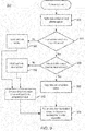
- Figure 9 is a flow chart of a method 900 for processing a load operation with the disclosed microarchitecture, according to an embodiment of the present disclosure.
- the method 900 may be performed by a system that may include hardware (e.g., circuitry, dedicated logic, and/or programmable logic), software (e.g., instructions executable on a computer system to perform hardware simulation), or a combination thereof.
- the method 900 may be performed by the memory ordering circuit 105 and various subcomponents of the memory ordering circuit 105.
- the method 900 may or may not use the disambiguation circuit 450, for example, and may incorporate disambiguation logic into the memory operations manager circuit 430 to perform the method 900.
- the disambiguation circuit 450 may also be used, as may be the disambiguator queue 452 (such as the CAM or counting Bloom filter).
- any of the input queues 416 and the completion queue 420 may be implemented as ring buffers.
- the method 900 may start with processing a load operation, with the memory ordering circuit 105 buffering a load address in the load address queue 522 (905). The method 900 may continue with determining whether the load address matches any of the store addresses stored in the store address queue 524 (910). If the answer is no, the method 900 may continue with the memory ordering circuit 105 sending the load operation onto the cache 12 (920) followed by placing the data received from the cache into the completion queue 542 (950). If the answer is yes, the method 900 may continue with the memory ordering circuit 105 determining whether data is available in the store data queue 526 for the store operation having the store address that matches the load address (930).
- the method 900 may continue with the memory ordering circuit 105 marking the load operation as a store forward pointing to the location in the store address queue 524 at which the data will be received from the acceleration hardware (940). Once the data does arrive, the method 900 may continue with the memory ordering circuit 105 enqueuing the data from the store forward into the completion queue 542 (950). The method 900 may then complete with the memory ordering circuit 105 returning the data, from the completion queue 542, to the acceleration hardware in response to the load request and in the order requested (970).
- the method 900 may continue with the memory ordering circuit 105 copying the data from the store address queue 526 to an in-order next slot in the completion queue 542 (960). The method 900 may then complete with the memory ordering circuit 105 returning the data, from the completion queue 542, to the acceleration hardware in response to the load request and in the order requested (970).
- the disambiguation logic of the memory ordering circuit 105 may copy data to the completion queue without issuing a command for the load operation to the memory subsystem 110, thus reducing latency and increasing throughput of performing memory operations on behalf of a processor.
- Figure 10 is a flow chart of a method 1000 for processing a store operation with the disclosed microarchitecture, according to an embodiment of the present disclosure.
- the method 1000 may be performed by a system that may include hardware (e.g., circuitry, dedicated logic, and/or programmable logic), software (e.g., instructions executable on a computer system to perform hardware simulation), or a combination thereof.
- the method 1000 may be performed by the memory ordering circuit 105 and various subcomponents of the memory ordering circuit 105.
- the method 1000 may or may not use the disambiguation circuit 450, for example, and may incorporate disambiguation logic into the memory operations manager circuit 430 to perform the method 1000.
- the disambiguation circuit 450 may also be used, as may be the disambiguator queue 452 (such as the CAM or counting Bloom filter).
- any of the input queues 416 and the completion queue 420 may be implemented as ring buffers.
- the method 1000 may start with processing a load operation, with the memory ordering circuit 105 buffering a store address into the store address queue 524 (1005). The method 1000 may continue with the memory ordering circuit 105 buffering store data for the store address into the store data queue 526 (1010). The method 1000 may continue with the memory ordering circuit 105 determining whether a load operation is pending within the input queues 416 that has the same address as the store address (1020). If the answer is yes, the method 1000 may continue with the memory ordering circuit 1030 enqueuing the data into the completion queue 542 for the load operation, which may then be completed (sent to the acceleration hardware) (1030).
- the method 1000 may continue with the memory ordering circuit 105 sending the store address and the data to the memory 18, to complete the store operation. If the answer is no at block 1020, the method 1000 may continue with the memory ordering circuit 105 directly sending the store address and the data to the memory 18, to complete the store operation (1040).
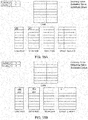
- Figure 11A is a diagrammatic representation of a content-addressable memory (CAM) 1150 implementation of the disambiguator circuit 450, according to an embodiment of the present disclosure.
- the disambiguator circuit 450 may store prior program-ordered memory accesses and may be queried for the presence of a particular address by using the CAM 1150 or a counting Bloom filter 1150' ( Figure 11B ), for example.
- the example of the CAM 1150 may be used for storing metadata (e.g., as entries) related to the pending memory operations associated with the prior program-ordered memory accesses.
- this metadata includes addresses (e.g., store addresses of pending store operations) and a corresponding input queue pointer, which may be determined based on dependency tokens indicating proper program order of incoming memory operations.
- the disambiguator circuit 450 may further store data associated with the store operations that are pending in the input queues, e.g., once the data is received from the acceleration hardware 102. Buffering the data may help in quickly and easily forwarding store data to the completion queue 542 for load operations, but the store data queue may also be directed (e.g., by the operations manager circuit 430) to forward that store data to the completion queue.
- the scheduler circuit 432 may store the metadata (store address and pointer to store data queue) into an entry of the CAM 1150. This forms a view of upcoming modifications to memory. Each store operation may be removed, once executed, but may be retained for a period of time (provided sufficient space in the CAM 1150) to continue to provide data forwarding for additional succeeding memory operations. The scheduler circuit 432 may then query the CAM 1150, and obtain a program-ordered view of the memory. Such a view may enable non-dependent load operations, e.g., that do not conflict with an entry in the CAM, to be sent to memory in parallel with completing the store operation.
- the scheduler circuit 432 may, for dependent load operations that do have an address conflict to an entry in the CAM, either stall, or preferred, perform data forwarding to the completion queue 420.
- access to the disambiguation circuit 450 may occur in legal program order as determined by ordering of dependency token flows.
- the memory ordering circuit 105 may track dependency token flows for dependent memory operations, even in the case where some memory operations have true data dependency.
- the disambiguator circuit 450 or the memory operations manager circuit 430 may forward data to dependent accesses, rather than issuing a memory operation to the memory 18, as illustrated with reference to Figures 9-10 .
- the disambiguator circuit 450 may provide an annotation for store operations to forward store data to dependent load operations when the store data becomes available.
- the use of pointers at such annotations has been discussed, but any sort of index or indicia may be used as well.
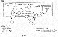
- Example flow annotations are depicted in Figure 12 , in which to service multiple dependent memory operations, the memory ordering circuit 105 chains together annotations such that dependent memory operations are served in subsequent cycles.
- FIG. 11B is a diagrammatic representation of counting Bloom filter 1150' implementation of a disambiguator circuit, according to an embodiment of the present disclosure.
- Bloom filters enable a concise representation of a set, in this case being represented as addresses of pending memory operations.
- a Bloom filter may result in false positives. If all h i return non-zero, additional checking may be performed.
- the operations manager circuit 430 may not expect a conflict, so this allows saving energy and area. In performing disambiguation without checking the CAM 1150, for example, this may improve scaling and energy use by checking a filter and storage structure 1118.
- the contents of the storage structure 1118 may include, but not be limited to, address tags (optional, used to eliminate filter false positives), an input queue pointer, and data (which, again, is option for use in forwarding.
- the operations manager circuit 430 may, as part of a first step, check a dependency token of a current memory operation, h i , with current dependency token counters 514. If there is a match ("present"), at a second step, the address of the memory operation may be compared with address tags of the storage structure 118, used to help identify and filter out false positives. If there is a tag match, at a third step, the operations manager circuit 430 has found a conflict in address of the memory operations (between one being scheduled and one that is pending or completed). The operations manager circuit 420 may then, at a fourth step, optionally forward data of a pending or completed store operation to a dependent (e.g., succeeding) store or load operation.
- serial structures may be used. For example, memory argument buffers within the operations queue 412 may be examined using a queue pointer rather than storing full address tags. This greatly reduces storage in the case that a partial address tag is stored, followed by a serial lookup of input queues.
- Figure 12 is a dataflow graph representation 1200 of a dependent loop illustrating dependency detection and forwarding using the disambiguator circuit 450, according to an embodiment of the present disclosure.
- a store address may flow into the load operation; and, a store address and a dependency token (N) may flow into the store operations (e.g., by way of the input queues 416) in a first step.
- the dependency token, N may indicate a dependency of the store operation on a previous memory operation.
- a further dependency token (N+1) may flow, in a subsequent step, between the store operation and the load operation to indicate the load operation depends on the completion of the store operation, e.g., wants to load data from the same address.
- an annotation may be provided to the disambiguator circuit (e.g., by the operations manager circuit 430) indicating a location in the store address queue 524 at which the store data will arrive. This may be any pointer, and in one embodiment, may be an index into the store data queue.
- the disambiguator circuit 450 may store an entry in the disambiguator queue 452 that includes the annotation and the store address. Also during the second step, dependency information flows between the store operation and the load operation.
- the operations manager circuit 430 may query the disambiguator circuit 450, and determine that there is an address conflict between the load operation and the store operation.
- the operations manager circuit 430 may then retrieve the entry for the store address, including the annotation or pointer, with which to perform store forwarding.
- the operations manager circuit may subsequently mark the load operation as a store forward, and generate a second annotation of a next in-order slot in the completion queue 542, to schedule the load operation.
- the second annotation may be performed by annotating the next in-order slot of the completion queue with the location of the pointer, so that the operations manager circuit 430 knows the location in the store data queue 526 from which to forward the data upon receipt of the data in the store data queue.
- FIG. 13A-13B An example of memory ordering and disambiguation by the memory ordering circuit 105 will be illustrated with a simplified example for purposes of explanation with relation to Figures 13A-13B , 14A-14B , and 15A-15I .
- the following code includes an array, p, which is accessed by indices i and i+2:
- the compiler annotates dependencies between two memory operations, load p[i] and store p[i+2]. Note that only sometimes do reads and writes conflict.
- the micro-architecture 500 is designed to extract memory-level parallelism where memory operations may move forward at the same time when there are no conflicts to the same address. This is especially the case for load operations, which expose latency in code execution due to waiting for preceding dependent store operations to complete.
- safe reorderings are noted by the arrows on the left of the unfolded code.
- microarchitecture may perform this reordering.
- further optimizations are obtained through use of the disambiguation circuit 450, which provides a program-ordered view of memory and opportunities to directly fulfill succeeding load operations that depend on data to be received for scheduled store operations.
- Figure 14A is a block diagram of exemplary memory arguments for a load operation 1402 and for a store operation 1404, according to an embodiment of the present disclosure. These, or similar, memory arguments were discussed with relation to Figure 8 and will not be repeated here. Note, however, that the store operation 1404 has no indicator for the output queue identifier because no data is being output to the acceleration hardware 102. Instead, the store address in channel 1 and the data in channel 2 of the input queues 416, as identified in the input queue identifier memory argument, are to be scheduled for transmission to the memory subsystem 110 in a memory command to complete the store operation 1404. Furthermore, the input channels and output channels of the dependency queues are both implemented with counters.
- the counters may be cycled between the load operations and the store operations within the flow of the code. Furthermore, note that both the load operation 1402 and the store operation 1404 are to use the CAM 1250 during performance of the memory ordering, as will be discussed.
- Figure 14B is a block diagram illustrating flow of the load operations and store operations, such as the load operation 1402 and the store 1404 operation of Figure 14A , through the microarchitecture 500 of the memory ordering circuit of Figure 5 , according to an embodiment of the present disclosure. For simplicity of explanation, not all of the components are displayed, but reference may be made back to the additional components displayed in Figure 5 .
- Various ovals indicating "Load” for the load operation 1402 and "Store” for the store operation 1404 are overlaid on some of the components of the microarchitecture 500 as indication of how various channels of the queues are being used as the memory operations are queued and ordered through the microarchitecture 500.
- the disambiguator circuit 450 such as the CAM 1250 for purposes of the present example.
- the disambiguator circuit 450 may be coupled to the operations manager circuit 430, to the input queue 416, and to the completion queue 420.
- the memory subsystem 110 is out of order.
- the operations manager circuit 430 may allocate an in-order next slot in an index of the completion queue 542 for each semantically-succeeding load operation. This indexed slot may be sent to the memory subsystem 110, so that a return value is correctly written to the completion buffer 542. Requiring each load operation to issue to memory, however, is not efficient for many programs.
- the disambiguator circuit 450 indicates that the load operation depends on a store operation that is pending, and has an entry in the disambiguator queue 452, the data may be forwarded from the store data queue 526. More specifically, when the operations manager circuit 430 queries the disambiguator circuit 450, the disambiguator circuit 450 may indicate an address conflict with a store operation. In this case, the operations manager circuit 430 may annotate (e.g., write) to the completion buffer index the location in the store data queue associated with the store operation on which the load operation depends. The operations manager circuit may perform the annotation by adding the pointer stored in the entry of the disambiguator queue 452 (for the store operation) in a memory address argument of the load operation during scheduling. After performing this annotation, the operations manager circuit 430 is said to have scheduled the load operation.
- the operations manager circuit 430 may perform the annotation by adding the pointer stored in the entry of the disambiguator queue 452 (for the store operation) in a memory address argument of the load operation during scheduling. After performing this annotation, the operations manager circuit
- the store operation is also considered scheduled, even if the data has not yet been received into the store data queue 526.
- the execution circuit 434 of the operations manager circuit 430 may detect the arrival of the data, forward the data to the indexed slot of the completion queue 542, and issue the store operation to the memory, including the store address and the data.
- the load operation may then complete, with the execution circuit 434 sending the forwarded data from the indexed slot in the completion queue into the acceleration hardware 102, as a load response.
- Figures 15A, 15B , 15C, 15D , 15E, 15F , 15G , 15H , and 15I are block diagrams illustrating functional flow of load operations and store operations for the exemplary program of Figures 13A and 13B through queues of the microarchitecture of Figure 14B , according to an embodiment of the present disclosure. Each figure may correspond to a next cycle of processing by the microarchitecture 500. Values that are italicized are incoming values (into the queues), values that are bolded are outgoing values (out of the queues), and values that are underlined are values that have been scheduled for completion. All other values with normal fonts are retained values already existing in the queues.
- address p[0] is bolded to indicate it is outgoing in this cycle.
- a new address p[1] is incoming into the load address queue and a new address p[3] is incoming into the store address queue.
- a zero ("0")-valued bit in the completion queue 542 is also incoming, which indicates any data present for that indexed entry is invalid.
- the value for the counter Cl is unchanged, and the value for counter C0 is bolded, indicating it is outgoing, corresponding to the outgoing load operation to address p[0].
- the address p[2] along with pointer "0" (pointing to the first slot in the store data queue) may be stored in an entry of the CAM, and are underlined to indicate that the entry is associated with the scheduled store operation to address p[2].
- the address p[2] for the newest (incoming) load operation is dependent on the value that first needs to be stored by the store operation for address p[2], which is at the top of the store address queue.
- the indexed entry in the completion queue for the load operation from address p[2] may be annotated to link to the store data queue to a location to receive data to be written to address p[2], to effect data forwarding ( Figure 15F ).
- the address p[1] in the load address queue is bolded to indicate it is outgoing to the memory.
- the corresponding "0" entry in the completion queue is likewise bolded as outgoing to the memory for address p[1].
- a new address p[3] is incoming into the load address queue and a new address p[5] is incoming into the store address queue.
- the values for the counters C0 and C1 have switched, and the value for counter C0 is bolded as also outgoing with the load operation from address p[1], and the value for counter C1 is indicated as incoming and associated with the new store operation to address p[5].
- the entry of address p[2] and pointer "0" remain in the CAM for the store operation to address p[2], as does the address p[2] in the store address queue, scheduled for completion.
- the completion queue has a value of "1" indicated as incoming from memory for load p[1] (which was sent out to the memory in Figure 15D ).
- the entry in the CAM for address p[2] and pointer "0" remains, and a new entry is stored in the CAM for store to address p[3], which includes pointer "1,” e.g., that points to index value one of the store data queue.
- pointer "1," e.g., that points to index value one of the store data queue.
- the store to address p[3] has also been scheduled, so these values are all underlined.
- a store forward may be performed by noting the data (valued "0") needed by the store operation from address p[2] (which is bolded to indicate it would be outgoing to the memory) may be forwarded from the pointer location "0" in the store data queue to the in-order next slot of the completion queue. This data is now in the second slot of the completion queue, and the data forwarding is indicated with the swirly line. Further, a new address p[5] is incoming into the load address queue and a new address p[7] is incoming into the store address queue.
- the address p[2] and pointer "0" in the first entry in the CAM are no longer underlined, but may be retained for potential future forwarding to a subsequent, dependent memory operation.
- the address p[3] and pointer "1" in the second entry in the CAM remain underlined as still being associated with scheduled store operation to p[3].
- a third entry may be stored in the CAM in conjunction with scheduling the store operation to address p[4] that includes pointer "2,” to indicate pointing to a third slot in the index of the store data queue.
- the address p[4] and pointer "2" are also, therefore, underlined to indicate being associated with scheduled store operation to address p[4].
- the address p[2] for the store operation in the store address queue is bolded, indicating it is outgoing with the data (valued "0") in the store data queue.
- the value "0" in the completion queue for the load operation to p[2] is outgoing, but this time to the acceleration hardware to complete the load operation from p[2] without sending a request to memory.
- the store data queue is also receiving data valued "1" for the store p[3].
- address p[6] is coming into the load address queue for a new load operation
- a new address p[8] is also incoming into the store address queue for a new store operation.
- the values of the counters C0 and C1 are again switched, and the value for counter C0 is incoming (corresponding to the new load operation to address p[6]) while the value for counter C1 is outgoing (corresponding to the outgoing store operation to p[2]).
- the load operation from address p[3] may complete, again with data forwarding, from the store data received into the store data queue for address p[3], as the load operation succeeds the store operation as indicated by the dependency tokens provided by the counters C0 and C1.
- the bolded "1" for counter C0 indicates outgoing dependency for the load operation to address p[3].
- the memory ordering circuit 105 furthermore, may first query the CAM to find the address conflict to address p[3] between the outgoing load operation and the scheduled store operation. The memory ordering circuit 105 may retrieve the pointer "1," and then forward the data stored in the store data queue corresponding to index "1" to the completion queue (shown again by the swirly line).
- a new address p[7] is incoming into the load address queue and a new address p[9] is incoming into the store address queue. Because the store address p[2] and store data (valued "0") are retained, the CAM, the store address queue, and the store data queue continue to fill up. Indeed, the store address queue is now full.
- the alternative embodiment of the CAM includes buffering the data for the store operation p[2] in the CAM itself. In this way, data may still be provided for address p[2] while still cleaning out indexed slots of the store address and data queues.
- the store address queue has run out of space to be able to queue address p[10] for the next store operation.
- the retained values for address p[2] may be evicted from the address and store data queues to make room to avoid stalling. This may be done in this case with no adverse effects because there are no foreseeable dependencies to address p[2] in the program, although any data buffered in the CAM for the store to address p[2] could optionally be retained (because the disambiguation queue is not yet full).
- the address p[3] and pointer "1" may still be retained in the CAM and the address p[3] and data (valued "1") may be retained in the store address and data queues.
- the entries to the store address and data queues for p[3] may then be evicted in the next cycle.
- the memory ordering circuit 105 need not reach the point of eviction so quickly, with the tradeoff being more hardware to perform the memory ordering and disambiguation.
- the address p[5] is underlined in the store address queue, to indicate that this store operation has now also been scheduled.
- An additional entry may be stored in the CAM that includes the address p[5] and a pointer "3" to indicate pointing to a fourth slot of an index of the store data queue.
- These values are also underlined to indicate that the associated store operation to address p[5] has been scheduled for completion.
- the data value "1" in the completion queue is bolded, as is the address p[3] in the load address queue, to indicate this load operation is outgoing to the acceleration hardware, performed with data forwarding in Figure 15H .
- the process of executing the code of Figures 13A and 13B may continue on with bouncing dependency tokens between "0" and "1" for the load operations and the store operations. This is due to the tight dependencies between p[i] and p[i+2]. Other code with less frequent dependencies may generate dependency tokens at a slower rate, and thus reset the counters C0 and C1 at a slower rate, causing the generation of tokens of higher values (corresponding to further semantically-separated memory operations).
- the microarchitecture 500 may also handle the reordering of store-store dependencies, load-load dependencies, and store-load dependencies with use of the disambiguation circuit 450, e.g., the CAM 1250.
- store-store reordering is valuable when a succeeding store has received its data and the preceding store has not. Thus, there is an opportunity to release the succeeding store early.
- a store-store dependency may be similar to the load-store: the dependent store checks for an address conflict against the CAM and may issue if no conflict is found.
- requests arising from the same memory operation are not re-ordered with respect to one another. Instead, these accesses may be guaranteed to be in order.
- the memory ordering circuit 105 may release a logically-succeeding store operation early, ahead of logically-preceding store operations, provided that the store operation checks the CAM 1250. The memory ordering circuit may still need to insert the store addresses, to check subsequent memory operations.
- the memory ordering circuit 105 may block issuance of the dependent store operation, because the dependent store operation sees the query address in the CAM and has no way of knowing that the dependency is not actually real.
- the operation manager circuit 430 may add some markers to CAM entries, for example, a bit vector encoding the memory operations that produced the address in the CAM 1250.
- the bit vector is a string of bits, with one bit representing each unique store operation that could be implemented on the memory interface at the same time.
- the bit vector is set to one ("1") if a particular memory operation has written the address associated with the entry in the CAM and zero ("0") if the address has not been written.
- the operations manager circuit 430 may know whether the conflict is real by checking the address and the bit vector in the CAM. If a different store operation produced the address, the conflict is real; otherwise, it is false. Bits in the bit vector are cleared when store operations to the associated address are sent to the memory subsystem. A CAM entry may be de-allocated when those operations have been sent and no bits in the bit vector are set. De-allocated entries may be reused by other store operations.
- FIG 16A is a block diagram illustrating a micro-architecture for a processor 1600 to perform operations of a processor or an integrated circuit that includes the memory subsystem 110 and the acceleration hardware 102 of Figures 1A-1B , according to an embodiment.
- processor 1600 depicts an in-order architecture core and a register renaming logic, out-of-order issue/execution logic to be included in a processor according to at least one embodiment of the disclosure.
- Processor 1600 includes a front end unit 1630 coupled to an execution engine unit 1650, and both are coupled to a memory unit 1670.
- the processor 1600 may include a reduced instruction set computing (RISC) core, a complex instruction set computing (CISC) core, a very long instruction word (VLIW) core, or a hybrid or alternative core type.
- processor 1600 may include a special-purpose core, such as, for example, a network or communication core, compression engine, graphics core, or the like.
- processor 1600 may be a multi-core processor or may be part of a multiprocessor system.
- the front end unit 1630 includes a branch prediction unit 1632 coupled to an instruction cache unit 1634, which is coupled to an instruction translation lookaside buffer (TLB) 1636, which is coupled to an instruction fetch unit 1638, which is coupled to a decode unit 1640.
- the decode unit 1640 (also known as a decoder) may decode instructions, and generate as an output one or more micro-operations, micro-code entry points, microinstructions, other instructions, or other control signals, which are decoded from, or which otherwise reflect, or are derived from, the original instructions.
- the decoder 1640 may be implemented using various different mechanisms.
- the instruction cache unit 1634 is further coupled to the memory unit 1670.
- the decode unit 1640 is coupled to a rename/allocator unit 1652 in the execution engine unit 1650.
- the execution engine unit 1650 includes the rename/allocator unit 1652 coupled to a retirement unit 1654 and a set of one or more scheduler circuit unit(s) 1656.
- the scheduler circuit unit(s) 1656 represents any number of different scheduler circuits, including reservations stations (RS), central instruction window, etc.
- the scheduler unit(s) 1656 is coupled to the physical register set(s) unit(s) 1658.
- Each of the physical register set(s) units 1658 represents one or more physical register sets, different ones of which store one or more different data types, such as scalar integer, scalar floating point, packed integer, packed floating point, vector integer, vector floating point, etc., status (e.g., an instruction pointer that is the address of the next instruction to be executed), etc.
- the physical register set(s) unit(s) 1658 is overlapped by the retirement unit 1654 to illustrate various ways in which register renaming and out-of-order execution may be implemented (e.g., using a reorder buffer(s) and a retirement register set(s), using a future file(s), a history buffer(s), and a retirement register set(s); using a register maps and a pool of registers; etc.).
- the architectural registers are visible from the outside of the processor or from a programmer's perspective.
- the registers are not limited to any known particular type of circuit.
- Various different types of registers are suitable as long as they are capable of storing and providing data as described herein. Examples of suitable registers include, but are not limited to, dedicated physical registers, dynamically allocated physical registers using register renaming, combinations of dedicated and dynamically allocated physical registers, etc.
- the retirement unit 1654 and the physical register set(s) unit(s) 1658 are coupled to the execution cluster(s) 1660.
- the execution cluster(s) 1660 includes a set of one or more execution units 1662 and a set of one or more memory access units 1664.
- the execution units 1662 may perform various operations (e.g., shifts, addition, subtraction, multiplication) and operate on various types of data (e.g., scalar floating point, packed integer, packed floating point, vector integer, vector floating point).
- While some embodiments may include a number of execution units dedicated to specific functions or sets of functions, other embodiments may include only one execution unit or multiple execution units that all perform all functions.
- the scheduler unit(s) 1656, physical register set(s) unit(s) 1658, and execution cluster(s) 1660 are shown as being possibly plural because certain embodiments create separate pipelines for certain types of data/operations (e.g., a scalar integer pipeline, a scalar floating point/packed integer/packed floating point/vector integer/vector floating point pipeline, and/or a memory access pipeline that each have their own scheduler unit, physical register set(s) unit, and/or execution cluster - and in the case of a separate memory access pipeline, certain embodiments are implemented in which only the execution cluster of this pipeline has the memory access unit(s) 1664). It should also be understood that where separate pipelines are used, one or more of these pipelines may be out-of-order issue/execution and the rest in-order.
- the set of memory access units 1664 is coupled to the memory unit 1670, which may include a data prefetcher 1680, a data TLB unit 1672, a data cache unit (DCU) 1674, and a level 2 (L2) cache unit 1676, to name a few examples.
- DCU 1674 is also known as a first level data cache (L1 cache).
- L1 cache first level data cache
- the DCU 1674 may handle multiple outstanding cache misses and continue to service incoming stores and loads. It also supports maintaining cache coherency.
- the data TLB unit 1672 is a cache used to improve virtual address translation speed by mapping virtual and physical address spaces.
- the memory access units 1664 may include a load unit, a store address unit, and a store data unit, each of which is coupled to the data TLB unit 1672 in the memory unit 1670.
- the L2 cache unit 1676 may be coupled to one or more other levels of cache and eventually to a main memory.
- the data prefetcher 1680 speculatively loads/prefetches data to the DCU 1674 by automatically predicting which data a program is about to consume.
- Prefetching may refer to transferring data stored in one memory location (e.g., position) of a memory hierarchy (e.g., lower level caches or memory) to a higher-level memory location that is closer (e.g., yields lower access latency) to the processor before the data is actually demanded by the processor. More specifically, prefetching may refer to the early retrieval of data from one of the lower level caches/memory to a data cache and/or prefetch buffer before the processor issues a demand for the specific data being returned.
- a memory hierarchy e.g., lower level caches or memory
- the processor 1600 may support one or more instructions sets (e.g., the x86 instruction set (with some extensions that have been added with newer versions); the MIPS instruction set of Imagination Technologies of Kings Langley, Hertfordshire, UK; the ARM instruction set (with optional additional extensions such as NEON) of ARM Holdings of Sunnyvale, CA).
- the x86 instruction set (with some extensions that have been added with newer versions); the MIPS instruction set of Imagination Technologies of Kings Langley, Hertfordshire, UK; the ARM instruction set (with optional additional extensions such as NEON) of ARM Holdings of Sunnyvale, CA).
- the core may support multithreading (executing two or more parallel sets of operations or threads), and may do so in a variety of ways including time sliced multithreading, simultaneous multithreading (where a single physical core provides a logical core for each of the threads that physical core is simultaneously multithreading), or a combination thereof (e.g., time sliced fetching and decoding and simultaneous multithreading thereafter such as in the Intel® Hyperthreading technology).
- register renaming is described in the context of out-of-order execution, it should be understood that register renaming may be used in an in-order architecture.
- the illustrated embodiment of the processor also includes a separate instruction and data cache units and a shared L2 cache unit, alternative embodiments may have a single internal cache for both instructions and data, such as, for example, a Level 1 (L1) internal cache, or multiple levels of internal cache.
- the system may include a combination of an internal cache and an external cache that is external to the core and/or the processor. Alternatively, all of the cache may be external to the core and/or the processor.
- instruction cache unit 1634, data cache unit 1674, and L2 cache unit 1676 would not generally implement the process described in this disclosure, as generally these cache units use on-die memory that does not exhibit page-locality behavior.
- Figure 16B is a block diagram illustrating an in-order pipeline and a register renaming stage, out-of-order issue/execution pipeline implemented by processor 1600 of Figure 16A according to some embodiments of the disclosure.
- the solid lined boxes in Figure 16B illustrate an in-order pipeline 1601, while the dashed lined boxes illustrate a register renaming, out-of-order issue/execution pipeline 1603.
- the pipelines 1601 and 1603 include a fetch stage 1602, a length decode stage 1604, a decode stage 1606, an allocation stage 1608, a renaming stage 1610, a scheduling (also known as a dispatch or issue) stage 1612, a register read/memory read stage 1614, an execute stage 1616, a write back/memory write stage 1618, an exception handling stage 1622, and a commit stage 1624.
- the ordering of stages 1602-1624 may be different than illustrated and are not limited to the specific ordering shown in Figure 16B .
- Figure 17 illustrates a block diagram of the micro-architecture for a processor 1700 that includes logic circuits of a processor or an integrated circuit that includes the memory subsystem 110 and the acceleration hardware 102 of Figures 1A-1B , according to an embodiment of the present disclosure.
- an instruction in accordance with one embodiment can be implemented to operate on data elements having sizes of byte, word, doubleword, quadword, etc., as well as datatypes, such as single and double precision integer and floating point datatypes.
- the in-order front end 1701 is the part of the processor 1700 that fetches instructions to be executed and prepares them to be used later in the processor pipeline.
- the embodiments of the page additions and content copying can be implemented in processor 1700.
- the front end 1701 may include several units.
- the instruction prefetcher 1716 fetches instructions from memory and feeds them to an instruction decoder 1718 which in turn decodes or interprets them.
- the decoder decodes a received instruction into one or more operations called "micro-instructions" or “micro-operations” (also called micro op or uops) that the machine can execute.
- the decoder parses the instruction into an opcode and corresponding data and control fields that are used by the micro-architecture to perform operations in accordance with one embodiment.
- the trace cache 1730 takes decoded uops and assembles them into program ordered sequences or traces in the uop queue 1734 for execution.
- microcode ROM (or RAM) 1732 provides the uops needed to complete the operation.
- the decoder 1718 accesses the microcode ROM 1732 to do the instruction.
- an instruction can be decoded into a small number of micro ops for processing at the instruction decoder 1718.
- an instruction can be stored within the microcode ROM 1732 should a number of micro-ops be needed to accomplish the operation.
- the trace cache 1730 refers to an entry point programmable logic array (PLA) to determine a correct micro-instruction pointer for reading the micro-code sequences to complete one or more instructions in accordance with one embodiment from the micro-code ROM 1732.
- the out-of-order execution engine 1703 is where the instructions are prepared for execution.
- the out-of-order execution logic has a number of buffers to smooth out and reorder the flow of instructions to optimize performance as they go down the pipeline and get scheduled for execution.
- the allocator logic allocates the machine buffers and resources that each uop needs in order to execute.
- the register renaming logic renames logic registers onto entries in a register set.
- the allocator also allocates an entry for each uop in one of the two uop queues, one for memory operations and one for non-memory operations, in front of the instruction schedulers: memory scheduler, fast scheduler 1702, slow/general floating point scheduler 1704, and simple floating point scheduler 1706.
- the uop schedulers 1702, 1704, 1706 determine when a uop is ready to execute based on the readiness of their dependent input register operand sources and the availability of the execution resources the uops need to complete their operation.
- the fast scheduler 1702 of one embodiment can schedule on each half of the main clock cycle while the other schedulers can only schedule once per main processor clock cycle.
- the schedulers arbitrate for the dispatch ports to schedule uops for execution.
- Register sets 1708, 1710 sit between the schedulers 1702, 1704, 1706, and the execution units 1712, 1714, 1716, 1718, 1720, 1722, 1724 in the execution block 1711.
- Each register set 1708, 1710, of one embodiment also includes a bypass network that can bypass or forward just completed results that have not yet been written into the register set to new dependent uops.
- the integer register set 1708 and the floating point register set 1710 are also capable of communicating data with the other.
- the integer register set 1708 is split into two separate register sets, one register set for the low order 32 bits of data and a second register set for the high order 32 bits of data.
- the floating point register set 1710 of one embodiment has 128 bit wide entries because floating point instructions typically have operands from 64 to 128 bits in width.
- the execution block 1711 contains the execution units 1712, 1714, 1716, 1718, 1720, 1722, 1724, where the instructions are actually executed.
- This section includes the register sets 1708, 1710, that store the integer and floating point data operand values that the micro-instructions need to execute.
- the processor 1700 of one embodiment is comprised of a number of execution units: address generation unit (AGU) 1712, AGU 1714, fast ALU 1716, fast ALU 1718, slow ALU 1720, floating point ALU 1712, floating point move unit 1714.
- AGU address generation unit
- the floating point execution blocks 1712, 1714 execute floating point, MMX, SIMD, and SSE, or other operations.
- the floating point ALU 1712 of one embodiment includes a 64 bit by 64 bit floating point divider to execute divide, square root, and remainder micro-ops. For embodiments of the present disclosure, instructions involving a floating point value may be handled with the floating point hardware.
- the ALU operations go to the high-speed ALU execution units 1716, 1718.
- the fast ALUs 1716, 1718, of one embodiment can execute fast operations with an effective latency of half a clock cycle.
- most complex integer operations go to the slow ALU 1720 as the slow ALU 1720 includes integer execution hardware for long latency type of operations, such as a multiplier, shifts, flag logic, and branch processing.
- Memory load/store operations are executed by the AGUs 1722, 1724.
- the integer ALUs 1716, 1718, 1720 are described in the context of performing integer operations on 64 bit data operands.
- the ALUs 1716, 1718, 1720 can be implemented to support a variety of data bits including 16, 32, 128, 256, etc.
- the floating point units 1722, 1724 can be implemented to support a range of operands having bits of various widths.
- the floating point units 1722, 1724 can operate on 128 bits wide packed data operands in conjunction with SIMD and multimedia instructions.
- the uops schedulers 1702, 1704, 1706 dispatch dependent operations before the parent load has finished executing.
- the processor 1700 also includes logic to handle memory misses. If a data load misses in the data cache, there can be dependent operations in flight in the pipeline that have left the scheduler with temporarily incorrect data.
- a replay mechanism tracks and re-executes instructions that use incorrect data. Only the dependent operations need to be replayed and the independent ones are allowed to complete.
- the schedulers and replay mechanism of one embodiment of a processor are also designed to catch instruction sequences for text string comparison operations.
- registers may refer to the on-board processor storage locations that are used as part of instructions to identify operands. In other words, registers may be those that are usable from the outside of the processor (from a programmer's perspective). However, the registers of an embodiment should not be limited in meaning to a particular type of circuit. Rather, a register of an embodiment is capable of storing and providing data, and performing the functions described herein.
- the registers described herein can be implemented by circuitry within a processor using any number of different techniques, such as dedicated physical registers, dynamically allocated physical registers using register renaming, combinations of dedicated and dynamically allocated physical registers, etc.
- integer registers store 32-bit integer data.
- a register set of one embodiment also contains eight multimedia SIMD registers for packed data.
- the registers are understood to be data registers designed to hold packed data, such as 64 bits wide MMXTM registers (also referred to as 'mm' registers in some instances) in microprocessors enabled with MMX technology from Intel Corporation of Santa Clara, California. These MMX registers, available in both integer and floating point forms, can operate with packed data elements that accompany SIMD and SSE instructions. Similarly, 128 bits wide XMM registers relating to SSE2, SSE3, SSE4, or beyond (referred to generically as "SSEx”) technology can also be used to hold such packed data operands.
- SSEx 128 bits wide XMM registers relating to SSE2, SSE3, SSE4, or beyond
- the registers do not need to differentiate between the two data types.
- integer and floating point are either contained in the same register set or different register sets.
- floating point and integer data may be stored in different registers or the same registers.
- multiprocessor system 1800 is a point-to-point interconnect system, and includes a first processor 1870 and a second processor 1880 coupled via a point-to-point interconnect 1850.
- processors 1870 and 1880 may be multicore processors, including first and second processor cores (i.e., processor cores 1874a and 1874b and processor cores 1884a and 1884b), although potentially many more cores may be present in the processors.
- processors 1870, 1880 While shown with two processors 1870, 1880, it is to be understood that the scope of the present disclosure is not so limited. In other implementations, one or more additional processors may be present in a given processor.
- Processors 1870 and 1880 are shown including integrated memory controller units 1872 and 1882, respectively.
- Processor 1870 also includes as part of its bus controller units point-to-point (P-P) interfaces 1876 and 1888; similarly, second processor 1880 includes P-P interfaces 1886 and 1888.
- Processors 1870, 1880 may exchange information via a point-to-point (P-P) interface 1850 using P-P interface circuits 1878, 1888.
- IMCs 1872 and 1882 couple the processors to respective memories, namely a memory 1832 and a memory 1834, which may be portions of main memory locally attached to the respective processors.
- Processors 1870, 1880 may each exchange information with a chipset 1890 via individual P-P interfaces 1852, 1854 using point to point interface circuits 1876, 1894, 1886, 1898.
- Chipset 1890 may also exchange information with a high-performance graphics circuit 1838 via a high-performance graphics interface 1839.
- a shared cache (not shown) may be included in either processor or outside of both processors, yet connected with the processors via P-P interconnect, such that either or both processors' local cache information may be stored in the shared cache if a processor is placed into a low power mode. Page locality may also be created in the shared cache across one or more cache controllers when allocating entries to the shared cache.
- first bus 1816 may be a Peripheral Component Interconnect (PCI) bus, or a bus such as a PCI Express bus or interconnect bus, although the scope of the present disclosure is not so limited.
- PCI Peripheral Component Interconnect
- FIG. 19 shown is a block diagram of a third system 1600 in accordance with an embodiment of the present disclosure.
- Like elements in Figures 18 and 19 bear like reference numerals, and certain aspects of Figure 19 have been omitted from Figure 18 in order to avoid obscuring other aspects of Figure 19 .
- FIG 19 illustrates that the processors 1970, 1980 may include integrated memory and I/O control logic ("CL") 1972 and 1992, respectively.
- CL 1972, 1982 may include integrated memory controller units such as described herein.
- CL 1972, 1992 may also include I/O control logic.
- Figure 19 illustrates that the memories 1932, 1934 are coupled to the CL 1972, 1992, and that I/O devices 1914 are also coupled to the control logic 1972, 1992.
- Legacy I/O devices 1915 are coupled to the chipset 1990.
- Figure 20 is an exemplary system on a chip (SoC) 2000 that may include one or more of the cores 2002A ...2002N.
- SoC system on a chip
- DSPs digital signal processors
- graphics devices video game devices
- set-top boxes micro controllers
- micro controllers cell phones
- portable media players hand held devices
- various other electronic devices are also suitable.
- a huge variety of systems or electronic devices capable of incorporating a processor and/or other execution logic as disclosed herein are generally suitable.
- An interconnect unit(s) 2002 may be coupled to: an application processor 2017 which includes a set of one or more cores 2002A-N and shared cache unit(s) 2006; a system agent unit 2010; a bus controller unit(s) 2016; an integrated memory controller unit(s) 2014; a set of one or more media processors 2020 which may include integrated graphics logic 2008, an image processor 2024 for providing still and/or video camera functionality, an audio processor 2026 for providing hardware audio acceleration, and a video processor 2028 for providing video encode/decode acceleration; a static random access memory (SRAM) unit 2030; a direct memory access (DMA) unit 2032; and a display unit 2040 for coupling to one or more external displays.
- an application processor 2017 which includes a set of one or more cores 2002A-N and shared cache unit(s) 2006
- a system agent unit 2010 includes a bus controller unit(s) 2016; an integrated memory controller unit(s) 2014; a set of one or more media processors 2020 which may include integrated graphics logic 2008, an image processor 2024
- SoC 2100 is included in user equipment (UE).
- UE refers to any device to be used by an end-user to communicate, such as a hand-held phone, smartphone, tablet, ultrathin notebook, notebook with broadband adapter, or any other similar communication device.
- a UE may connect to a base station or node, which can correspond in nature to a mobile station (MS) in a GSM network.
- MS mobile station
- the embodiments of the page additions and content copying can be implemented in SoC 2100.
- SoC 2100 includes 2 cores-2106 and 2107. Similar to the discussion above, cores 2106 and 2107 may conform to an Instruction Set Architecture, such as a processor having the Intel® Architecture CoreTM, an Advanced Micro Devices, Inc. (AMD) processor, a MIPS-based processor, an ARM-based processor design, or a customer thereof, as well as their licensees or adopters. Cores 2106 and 2107 are coupled to cache control 2108 that is associated with bus interface unit 2109 and L2 cache 2110 to communicate with other parts of system 2100. Interconnect 2111 includes an on-chip interconnect, such as an IOSF, AMBA, or other interconnects discussed above, which can implement one or more aspects of the described disclosure.
- an Instruction Set Architecture such as a processor having the Intel® Architecture CoreTM, an Advanced Micro Devices, Inc. (AMD) processor, a MIPS-based processor, an ARM-based processor design, or a customer thereof, as well as their licensees or adopters.
- Cores 2106 and 2107 are coupled to cache
- SDRAM controller 2140 may connect to interconnect 2111 via cache 2110.
- Interconnect 2111 provides communication channels to the other components, such as a Subscriber Identity Module (SIM) 2130 to interface with a SIM card, a boot ROM 2135 to hold boot code for execution by cores 2106 and 2107 to initialize and boot SoC 2100, a SDRAM controller 2140 to interface with external memory (e.g. DRAM 2160), a flash controller 2145 to interface with non-volatile memory (e.g. Flash 2165), a peripheral control 2150 (e.g. Serial Peripheral Interface) to interface with peripherals, video codecs 2120 and Video interface 2125 to display and receive input (e.g. touch enabled input), GPU 2115 to perform graphics related computations, etc. Any of these interfaces may incorporate aspects of the embodiments described herein.
- SIM Subscriber Identity Module
- boot ROM 2135 to hold boot code for execution by cores 2106 and 2107 to initialize and boot SoC 2100
- SDRAM controller 2140 to interface with external
- peripherals for communication such as a Bluetooth® module 2170, 3G modem 2175, GPS 2180, and Wi-Fi® 2185.
- a UE includes a radio for communication.
- these peripheral communication modules may not all be included.
- some form of a radio for external communication should be included.
- Figure 22 illustrates a diagrammatic representation of a machine in the example form of a computing system 2200 within which a set of instructions, for causing the machine to perform any one or more of the methodologies discussed herein, may be executed.
- the machine may be connected (e.g., networked) to other machines in a LAN, an intranet, an extranet, or the Internet.
- the machine may operate in the capacity of a server or a client device in a client-server network environment, or as a peer machine in a peer-to-peer (or distributed) network environment.
- the machine may be a personal computer (PC), a tablet PC, a set-top box (STB), a Personal Digital Assistant (PDA), a cellular telephone, a web appliance, a server, a network router, switch or bridge, or any machine capable of executing a set of instructions (sequential or otherwise) that specify actions to be taken by that machine.
- PC personal computer
- PDA Personal Digital Assistant
- STB set-top box
- WPA Personal Digital Assistant
- a cellular telephone a web appliance
- server a server
- network router switch or bridge
- any machine capable of executing a set of instructions (sequential or otherwise) that specify actions to be taken by that machine.
- machine shall also be taken to include any collection of machines that individually or jointly execute a set (or multiple sets) of instructions to perform any one or more of the methodologies discussed herein.
- the embodiments of the page additions and content copying can be implemented in computing system 2200.
- the computing system 2200 includes a processing device 2202, main memory 2204 (e.g., flash memory, dynamic random access memory (DRAM) (such as synchronous DRAM (SDRAM) or DRAM (RDRAM), etc.), a static memory 2206 (e.g., flash memory, static random access memory (SRAM), etc.), and a data storage device 2218, which communicate with each other via a bus 2208.
- main memory 2204 e.g., flash memory, dynamic random access memory (DRAM) (such as synchronous DRAM (SDRAM) or DRAM (RDRAM), etc.
- static memory 2206 e.g., flash memory, static random access memory (SRAM), etc.
- SRAM static random access memory
- Processing device 2202 represents one or more general-purpose processing devices such as a microprocessor, central processing unit, or the like. More particularly, the processing device may be complex instruction set computing (CISC) microprocessor, reduced instruction set computer (RISC) microprocessor, very long instruction word (VLIW) microprocessor, or processor implementing other instruction sets, or processors implementing a combination of instruction sets. Processing device 2202 may also be one or more special-purpose processing devices such as an application-specific integrated circuit (ASIC), a field programmable gate array (FPGA), a digital signal processor (DSP), network processor, or the like. In one embodiment, processing device 2202 may include one or more processor cores. The processing device 2202 is configured to execute the processing logic 2226 for performing the operations discussed herein.
- CISC complex instruction set computing
- RISC reduced instruction set computer
- VLIW very long instruction word
- processing device 2202 may also be one or more special-purpose processing devices such as an application-specific integrated circuit (ASIC), a field programmable gate array (F
- processing device 2202 can be part of a processor or an integrated circuit that includes the memory subsystem and the acceleration hardware of Figures 1A-1B .
- the computing system 2200 can include other components as described herein.
- the core may support multithreading (executing two or more parallel sets of operations or threads), and may do so in a variety of ways including time sliced multithreading, simultaneous multithreading (where a single physical core provides a logical core for each of the threads that physical core is simultaneously multithreading), or a combination thereof (e.g., time sliced fetching and decoding and simultaneous multithreading thereafter such as in the Intel® Hyperthreading technology).
- the computing system 2200 may further include a network interface device 2218 communicably coupled to a network 2219.
- the computing system 2200 also may include a video display device 2210 (e.g., a liquid crystal display (LCD) or a cathode ray tube (CRT)), an alphanumeric input device 2210 (e.g., a keyboard), a cursor control device 2214 (e.g., a mouse), a signal generation device 2220 (e.g., a speaker), or other peripheral devices.
- video display device 2210 e.g., a liquid crystal display (LCD) or a cathode ray tube (CRT)
- an alphanumeric input device 2210 e.g., a keyboard
- a cursor control device 2214 e.g., a mouse
- signal generation device 2220 e.g., a speaker
- computing system 2200 may include a graphics processing unit 2222, a video processing unit 2228 and an audio processing unit 2232.
- the computing system 2200 may include a chipset (not illustrated), which refers to a group of integrated circuits, or chips, that are designed to work with the processing device 2202 and controls communications between the processing device 2202 and external devices.
- the chipset may be a set of chips on a motherboard that links the processing device 2202 to very high-speed devices, such as main memory 2204 and graphic controllers, as well as linking the processing device 2202 to lower-speed peripheral buses of peripherals, such as USB, PCI or ISA buses.
- the data storage device 2218 may include a computer-readable storage medium 2224 on which is stored software 2226 embodying any one or more of the methodologies of functions described herein.
- the software 2226 may also reside, completely or at least partially, within the main memory 2204 as instructions 2226 and/or within the processing device 2202 as processing logic during execution thereof by the computing system 2200; the main memory 2204 and the processing device 2202 also constituting computer-readable storage media.
- the computer-readable storage medium 2224 may also be used to store instructions 2226 utilizing the processing device 2202, and/or a software library containing methods that call the above applications. While the computer-readable storage medium 2224 is shown in an example embodiment to be a single medium, the term "computer-readable storage medium” should be taken to include a single medium or multiple media (e.g., a centralized or distributed database, and/or associated caches and servers) that store the one or more sets of instructions. The term “computer-readable storage medium” shall also be taken to include any medium that is capable of storing, encoding or carrying a set of instruction for execution by the machine and that cause the machine to perform any one or more of the methodologies of the present embodiments. The term “computer-readable storage medium” shall accordingly be taken to include, but not be limited to, solid-state memories, and optical and magnetic media.
- Example 1 is an integrated circuit comprising: 1) a processor to execute instructions of a program and to interact with a memory; 2) acceleration hardware to execute a sub-program corresponding to the instructions; 3) a set of input queues coupled to the acceleration hardware and to the memory, the set of input queues comprising: a) a store address queue to receive, from the acceleration hardware, a first address of the memory, the first address associated with a store operation; and b) a store data queue to receive, from the acceleration hardware, first data to be stored at the first address of the memory; 4) a completion queue to buffer response data for a load operation; and 5) a disambiguator circuit coupled to the set of input queues and the completion queue, the disambiguator circuit to, responsive to determining the load operation that succeeds the store operation has an address conflict with the first address, copy the first data from the store data queue into the completion queue for the load operation.
- Example 2 the integrated circuit of Example 1, further comprising an operations queue coupled to the set of input queues, the operations queue to buffer address arguments for the store operation and the load operation, comprising: a) a channel of the set of input queues at which to retrieve the first address for the store operation; and b) a second channel of the set of input queues at which to retrieve the first address for the load operation.
- Example 3 the integrated circuit of Example 1, further comprising a scheduler circuit coupled to the set of input queues and to a memory interface, the scheduler circuit to: a) schedule issuance of the store operation upon receipt of the first address; and b) trigger generation of a dependency token to indicate, to the load operation, a dependency on the first data stored by the store operation
- Example 4 the integrated circuit of Example 3, further comprising an execution circuit coupled to the scheduler circuit, to the set of input queues, and to the memory, the execution circuit to, upon detecting reception of the first data in the store data queue, issue the store operation to the memory with the dependency token, to store the first data at the first address.
- Example 5 the integrated circuit of Example 3, wherein the disambiguator circuit comprises a content-addressable memory (CAM), and the scheduler circuit is further to store an entry in the CAM, the entry comprising the first address and a pointer into the store data queue to a location at which to receive the first data.
- CAM content-addressable memory
- Example 6 the integrated circuit of Example 5, wherein the disambiguator circuit is further to stall in response to the CAM filling up with entries for scheduled store operations.
- Example 7 the integrated circuit of Example 5, wherein the scheduler circuit is further to, upon receipt of the first data in the store data queue, store the first data in the CAM in association with the entry, and wherein the disambiguator circuit is to retain the first data in a disambiguator queue of the disambiguator circuit, the first data to be forwarded to a subsequent memory operation that succeeds the load operation.
- Example 8 the integrated circuit of Example 5, wherein the set of input queues further comprises a load address queue to receive, from the acceleration hardware, the first address for the load operation, and wherein the scheduler circuit is further to: a) detect, based on a search of the CAM, an address conflict between the load operation and the store operation; b) retrieve the pointer from the CAM; and c) annotate an indexed slot of the completion queue with the location in the pointer, to schedule issuance of the load operation upon receipt of the data at the location of the store data queue.
- Example 9 the integrated circuit of Example 1, wherein one of the set of input queues and the completion queue is a ring buffer.
- Example 10 is a memory ordering circuit comprising: 1) a memory interface coupled to a memory, the memory to store data corresponding to instructions being executed for a program; 2) an operations queue coupled to the memory interface, the operations queue to buffer memory operations corresponding to the instructions; 3) a set of input queues coupled to the memory interface and to acceleration hardware, which is to execute a sub-program corresponding to the instructions, the set of input queues comprising: a) a store address queue to receive, from the acceleration hardware, a first address of the memory for a store operation of the memory operations; and b) a store data queue to receive, from the acceleration hardware, first data to be stored at the first address in completion of the store operation; 4) a disambiguator circuit coupled to the set of input queues, the disambiguator circuit including a disambiguator queue; and 5) an operations manager circuit coupled to the set of input queues and the disambiguator circuit, the operations manager circuit to: a) schedule the store operation to issue to the memory upon receipt of the first address; and b) store an
- Example 11 the memory ordering circuit of Example 10, wherein the disambiguator circuit comprises one of a disambiguation content-addressable memory (CAM) or a counting Bloom filter.
- CAM disambiguation content-addressable memory
- Example 12 the memory ordering circuit of Example 10, wherein the set of input queues further comprises a load address queue to receive a second address, from the acceleration hardware, for a succeeding load operation, wherein the operation manager is further to: a) detect, based on a search requested of the disambiguator circuit, no address conflict between the store operation and the succeeding load operation; and b) issue the load operation to the memory without waiting for completion of the store operation.
- Example 13 the memory ordering circuit of Example 10, wherein the set of input queues further comprises a load address queue to receive the first address, from the acceleration hardware, for a load operation that succeeds the store operation, further comprising: 1) a completion queue coupled to the operations manager circuit and to the memory, the completion queue to enqueue data received for completion of the load operation; and 2) a dependency queue coupled to the acceleration hardware and to receive, from the acceleration hardware, a dependency token associated with the first address for the load operation, the dependency token indicating a dependency on the first data to be stored by the store operation.
- Example 14 the memory ordering circuit of Example 13, wherein the completion queue is a ring buffer.
- Example 15 the memory ordering circuit of Example 13, wherein the operations manager circuit is further to: a) detect, based on a search requested of the disambiguator circuit, an address conflict between the load operation and the store operation; b) retrieve the pointer from the disambiguator queue; and c) annotate an indexed slot of the completion queue with the location of the pointer, to schedule issuance of the load operation upon receipt of the data at the location in the store data queue.
- Example 16 the memory ordering circuit of Example 15, wherein the operations manager circuit is further to: a) detect arrival of the first data at the location of the pointer into the store data queue; and b) enqueue the data, from the location in the store data queue, into the indexed slot of the completion queue, to thereby complete data forwarding to the load operation.
- Example 17 the memory ordering circuit of Example 13, further comprising an operations queue coupled to the operations manager circuit and to the memory interface, the operations queue to buffer the load operation and the store operation, each of which comprise a memory argument containing an indication of whether to interact with the disambiguator circuit, wherein the operations manager circuit is further to, responsive to detecting the indication to access the disambiguator circuit: a) direct the disambiguator circuit to store the entry for the store operation; and b) check the disambiguator circuit for an address conflict between the store operation and the load operation
- Example 18 the memory ordering circuit of Example 10, wherein the operations manager circuit is further to: a) trigger generation of a dependency token to indicate, to a succeeding dependent memory operation, a dependency on the data stored by the store operation; and b) in response to detecting receipt of the first data into the store data queue, issue a store command containing the dependency token directed to the first address in the memory.
- Example 19 is a method comprising: 1) queuing memory operations in an operations queue of a memory ordering circuit, the memory operations directed towards a memory in association with acceleration hardware; 2) receiving, into a load address queue of a set of input queues, a load address received from the acceleration hardware for a load operation of the memory operations; 3) determining, by a disambiguator circuit, the load address matches a store address buffered in a store address queue for a store operation of the memory operations, the store operation preceding the load operation according to program order; and 4) marking, by the memory ordering circuit and in response to the determining, the load operation as a store forward with a pointer to a location, within a store data queue of the set of input queues, for reception of data to complete the store operation and the load operation.
- Example 20 the method of Example 19, further comprising: 1) scheduling the store operation to issue to the memory upon receipt of the store address; and 2) storing an entry in a disambiguator queue of the disambiguator circuit, the entry comprising the store address and the pointer.
- Example 21 the method of Example 20, further comprising: 1) storing the data in the disambiguator queue in association with the entry, in response to receiving the data into the store data queue; and 2) retaining the data, in the disambiguator queue, to be forwarded to a subsequent memory operation that succeeds the load operation
- Example 22 the method of Example 20, further comprising, in response to receiving the data into the location of the store data queue: 1) copying the data, from the location in the store data queue, into an indexed slot of a completion queue for the load operation; 2) issuing the store operation to the memory to complete the store operation; and 3) sending the data, from the completion queue, to the acceleration hardware in response to the load operation.
- Example 23 the method of Example 22, further comprising retaining the data, in the store data queue, after completion of the store operation, to fulfill at least a second load operation.
- Example 24 the method of Example 22, further comprising: 1) receiving, in a dependency queue of the set of input queues, a dependency token associated with the load address buffered in the load address queue, the dependency token indicating dependency on the data stored by the store operation; 2) duplicating the dependency token for a subsequent memory operation that is dependent on the load operation; and 3) wherein the sending the data to the acceleration hardware further comprises sending the dependency token with the data to the acceleration hardware, to complete the load operation.
- the embodiments are described with reference to determining validity of data in cache lines of a sector-based cache in specific integrated circuits, such as in computing platforms or microprocessors.
- the embodiments may also be applicable to other types of integrated circuits and programmable logic devices.
- the disclosed embodiments are not limited to desktop computer systems or portable computers, such as the Intel® UltrabooksTM computers.
- the disclosed embodiments are not limited to desktop computer systems or portable computers, such as the Intel® UltrabooksTM computers.
- handheld devices tablets, other thin notebooks, systems on a chip (SoC) devices, and embedded applications.
- Some examples of handheld devices include cellular phones, Internet protocol devices, digital cameras, personal digital assistants (PDAs), and handheld PCs.
- Embedded applications typically include a microcontroller, a digital signal processor (DSP), a system on a chip, network computers (NetPC), set-top boxes, network hubs, wide area network (WAN) switches, or any other system that can perform the functions and operations taught below. It is described that the system can be any kind of computer or embedded system.
- the disclosed embodiments may especially be used for low-end devices, like wearable devices (e.g., watches), electronic implants, sensory and control infrastructure devices, controllers, supervisory control and data acquisition (SCADA) systems, or the like.
- the apparatuses, methods, and systems described herein are not limited to physical computing devices, but may also relate to software optimizations for energy conservation and efficiency.
- the embodiments of methods, apparatuses, and systems described herein are vital to a 'green technology' future balanced with performance considerations.
- embodiments herein are described with reference to a processor, other embodiments are applicable to other types of integrated circuits and logic devices. Similar techniques and teachings of embodiments of the present disclosure can be applied to other types of circuits or semiconductor devices that can benefit from higher pipeline throughput and improved performance.
- the teachings of embodiments of the present disclosure are applicable to any processor or machine that performs data manipulations. However, the present disclosure is not limited to processors or machines that perform 512 bit, 256 bit, 128 bit, 64 bit, 32 bit, or 16 bit data operations and can be applied to any processor and machine in which manipulation or management of data is performed.
- the description herein provides examples, and the accompanying drawings show various examples for the purposes of illustration. However, these examples should not be construed in a limiting sense as they are merely intended to provide examples of embodiments of the present disclosure rather than to provide an exhaustive list of all possible implementations of embodiments of the present disclosure.
- Embodiments of the present disclosure may be provided as a computer program product or software which may include a machine or computer-readable medium having stored thereon instructions which may be used to program a computer (or other electronic devices) to perform one or more operations according to embodiments of the present disclosure.
- operations of embodiments of the present disclosure might be performed by specific hardware components that contain fixed-function logic for performing the operations, or by any combination of programmed computer components and fixed-function hardware components.
- a machine-readable medium may include any mechanism for storing or transmitting information in a form readable by a machine (e.g., a computer), but is not limited to, floppy diskettes, optical disks, Compact Disc, Read-Only Memory (CD-ROMs), and magneto-optical disks, Read-Only Memory (ROMs), Random Access Memory (RAM), Erasable Programmable Read-Only Memory (EPROM), Electrically Erasable Programmable Read-Only Memory (EEPROM), magnetic or optical cards, flash memory, or a tangible, machine-readable storage used in the transmission of information over the Internet via electrical, optical, acoustical or other forms of propagated signals (e.g., carrier waves, infrared signals, digital signals, etc.). Accordingly, the computer-
- a design may go through various stages, from creation to simulation to fabrication.
- Data representing a design may represent the design in a number of manners.
- the hardware may be represented using a hardware description language or another functional description language.
- a circuit level model with logic and/or transistor gates may be produced at some stages of the design process.
- most designs, at some stage reach a level of data representing the physical placement of various devices in the hardware model.
- the data representing the hardware model may be the data specifying the presence or absence of various features on different mask layers for masks used to produce the integrated circuit.
- the data may be stored in any form of a machine readable medium.
- a memory or a magnetic or optical storage such as a disc may be the machine readable medium to store information transmitted via optical or electrical wave modulated or otherwise generated to transmit such information.
- an electrical carrier wave indicating or carrying the code or design is transmitted, to the extent that copying, buffering, or re-transmission of the electrical signal is performed, a new copy is made.
- a communication provider or a network provider may store on a tangible, machine-readable medium, at least temporarily, an article, such as information encoded into a carrier wave, embodying techniques of embodiments of the present disclosure.
- a module as used herein refers to any combination of hardware, software, and/or firmware.
- a module includes hardware, such as a micro-controller, associated with a non-transitory medium to store code adapted to be executed by the micro-controller. Therefore, reference to a module, in one embodiment, refers to the hardware, which is specifically configured to recognize and/or execute the code to be held on a non-transitory medium.
- use of a module refers to the non-transitory medium including the code, which is specifically adapted to be executed by the microcontroller to perform predetermined operations.
- the term module in this example may refer to the combination of the microcontroller and the non-transitory medium.
- a first and a second module may share hardware, software, firmware, or a combination thereof, while potentially retaining some independent hardware, software, or firmware.
- use of the term logic includes hardware, such as transistors, registers, or other hardware, such as programmable logic devices.
- phrase 'configured to,' in one embodiment refers to arranging, putting together, manufacturing, offering to sell, importing and/or designing an apparatus, hardware, logic, or element to perform a designated or determined task.
- an apparatus or element thereof that is not operating is still 'configured to' perform a designated task if it is designed, coupled, and/or interconnected to perform said designated task.
- a logic gate may provide a 0 or a 1 during operation.
- a logic gate 'configured to' provide an enable signal to a clock does not include every potential logic gate that may provide a 1 or 0. Instead, the logic gate is one coupled in some manner that during operation the 1 or 0 output is to enable the clock.
- use of the phrases 'to,' 'capable of/to,' and/or 'operable to,' in one embodiment refers to some apparatus, logic, hardware, and/or element designed in such a way to enable use of the apparatus, logic, hardware, and/or element in a specified manner.
- use of 'to,' 'capable to,' or 'operable to,' in one embodiment refers to the latent state of an apparatus, logic, hardware, and/or element, where the apparatus, logic, hardware, and/or element is not operating but is designed in such a manner to enable use of an apparatus in a specified manner.
- a value includes any known representation of a number, a state, a logical state, or a binary logical state. Often, the use of logic levels, logic values, or logical values is also referred to as 1's and 0's, which simply represents binary logic states. For example, a 1 refers to a high logic level and 0 refers to a low logic level.
- a storage cell such as a transistor or flash cell, may be capable of holding a single logical value or multiple logical values.
- the decimal number ten may also be represented as a binary value of 1010 and a hexadecimal letter A. Therefore, a value includes any representation of information capable of being held in a computer system.
- states may be represented by values or portions of values.
- a first value such as a logical one
- a second value such as a logical zero
- reset and set in one embodiment, refer to a default and an updated value or state, respectively.
- a default value potentially includes a high logical value, i.e. reset
- an updated value potentially includes a low logical value, i.e. set.
- any combination of values may be utilized to represent any number of states.
- a non-transitory machine-accessible/readable medium includes any mechanism that provides (i.e., stores and/or transmits) information in a form readable by a machine, such as a computer or electronic system.
- a non-transitory machine-accessible medium includes random-access memory (RAM), such as static RAM (SRAM) or dynamic RAM (DRAM); ROM; magnetic or optical storage medium; flash memory devices; electrical storage devices; optical storage devices; acoustical storage devices; other form of storage devices for holding information received from transitory (propagated) signals (e.g., carrier waves, infrared signals, digital signals); etc., which are to be distinguished from the non-transitory mediums that may receive information there from.
- RAM random-access memory
- SRAM static RAM
- DRAM dynamic RAM
- a machine-readable medium may include any mechanism for storing or transmitting information in a form readable by a machine (e.g., a computer), but is not limited to, floppy diskettes, optical disks, Compact Disc, Read-Only Memory (CD-ROMs), and magneto-optical disks, Read-Only Memory (ROMs), Random Access Memory (RAM), Erasable Programmable Read-Only Memory (EPROM), Electrically Erasable Programmable Read-Only Memory (EEPROM), magnetic or optical cards, flash memory, or a tangible, machine-readable storage used in the transmission of information over the Internet via electrical, optical, acoustical or other forms of propagated signals (e.g., carrier waves, infrared signals, digital signals, etc.). Accordingly, the computer-
- example or “exemplary” are used herein to mean serving as an example, instance or illustration. Any aspect or design described herein as “example' or “exemplary” is not necessarily to be construed as preferred or advantageous over other aspects or designs. Rather, use of the words “example” or “exemplary” is intended to present concepts in a concrete fashion.
- the term “or” is intended to mean an inclusive “or” rather than an exclusive “or.” That is, unless specified otherwise, or clear from context, "X includes A or B” is intended to mean any of the natural inclusive permutations. That is, if X includes A; X includes B; or X includes both A and B, then "X includes A or B" is satisfied under any of the foregoing instances.
Landscapes
- Engineering & Computer Science (AREA)
- Theoretical Computer Science (AREA)
- Physics & Mathematics (AREA)
- General Engineering & Computer Science (AREA)
- General Physics & Mathematics (AREA)
- Software Systems (AREA)
- Human Computer Interaction (AREA)
- Computer Security & Cryptography (AREA)
- Advance Control (AREA)
Abstract
Description
- The present disclosure relates to the acceleration hardware, and in particular, to runtime address disambiguation in acceleration hardware such as spatial arrays.
- Acceleration hardware refers to devices that speed up data communications, storage and retrieval, encryption and decryption, mathematical operations, graphics, Web page viewing, and the like. Acceleration hardware may include individual integrated circuit (also called an IC or chip), a printed circuit card, or a self-contained system. A few examples of acceleration hardware include a network access accelerator (NAS), a graphics accelerator, and a floating point accelerator (FPA). In one embodiment, acceleration hardware is instantiated as spatial architecture, which is energy efficient and a high-performance means of accelerating user applications in computing systems using spatial arrays. A spatial architecture includes an array of processing components, such as gates in a Field Programmable Gate Array (FPGA) or other processing elements (PE).
-
-
Figure 1A is a block diagram of a system that employs a memory ordering circuit interposed between a memory subsystem and acceleration hardware, according to an embodiment of the present disclosure. -
Figure 1B is a block diagram of the system ofFigure 1A , but which employs multiple memory ordering circuits, according to an embodiment of the present disclosure. -
Figure 2 is a block diagram illustrating general functioning of memory operations into and out of acceleration hardware, according to an embodiment of the present disclosure. -
Figure 3 is a block diagram illustrating a spatial dependency flow for a store operation, according to an embodiment of the present disclosure. -
Figure 4 is a detailed block diagram of the memory ordering circuit ofFigure 1 , according to an embodiment of the present disclosure. -
Figure 5 is a flow diagram of a microarchitecture of the memory ordering circuit ofFigure 1 , according to an embodiment of the present disclosure. -
Figure 6 is a block diagram of an executable determiner circuit, according to an embodiment of the present disclosure. -
Figure 7 is a block diagram of a priority encoder, according to an embodiment of the present disclosure. -
Figure 8 is a block diagram of an exemplary load instruction, both logical and in binary, according to an embodiment of the present disclosure. -
Figure 9 is a flow chart of a method for processing a load operation with the disclosed microarchitecture, according to an embodiment of the present disclosure. -
Figure 10 is a flow chart of a method for processing a store operation with the disclosed microarchitecture, according to an embodiment of the present disclosure. -
Figure 11A is a diagrammatic representation of a content-addressable memory (CAM) implementation of a disambiguator circuit, according to an embodiment of the present disclosure. -
Figure 11B is a diagrammatic representation of counting Bloom filter implementation of a disambiguator circuit, according to an embodiment of the present disclosure. -
Figure 12 is a dataflow graph representation of a dependent loop illustrating dependency detection and forwarding using the disambiguator circuit, according to an embodiment of the present disclosure. -
Figure 13A is flow diagram illustrating logical execution of an example code, according to an embodiment of the present disclosure. -
Figure 13B is the flow diagram ofFigure 9A , illustrating memory-level parallelism in an unfolded version of the example code, according to an embodiment of the present disclosure. -
Figure 14A is a block diagram of exemplary memory arguments for a load operation and for a store operation, according to an embodiment of the present disclosure. -
Figure 14B is a block diagram illustrating flow of load operations and the store operations, such as those ofFigure 14A , through the disclosed microarchitecture and disambiguator circuit, according to an embodiment of the present disclosure. -
Figures 15A, 15B ,15C, 15D ,15E, 15F ,15G ,15H , and15I are block diagrams illustrating functional flow of load operations and store operations for an exemplary program through queues and the disambiguator circuit of the microarchitecture ofFigure 14B , according to an embodiment of the present disclosure. -
Figure 16A is a block diagram illustrating an in-order pipeline and a register renaming stage, out-of-order issue/execution pipeline according to one embodiment. -
Figure 16B is a block diagram illustrating a micro-architecture for a processor or an integrated circuit that includes the memory subsystem and the acceleration hardware ofFigures 1A-1B , according to an embodiment of the present disclosure. -
Figure 17 illustrates a block diagram of the micro-architecture for a processor or an integrated circuit that includes the memory subsystem and the acceleration hardware ofFigures 1A-1B , according to an embodiment of the present disclosure. -
Figure 18 is a block diagram of a computer system according to one implementation. -
Figure 19 is a block diagram of a computer system according to another implementation. -
Figure 20 is a block diagram of a system-on-a-chip according to one implementation. -
Figure 21 illustrates another implementation of a block diagram for a computing system. -
Figure 22 illustrates another implementation of a block diagram for a computing system. - Disclosed is architecture for describing memory ordering dependencies within acceleration hardware. As discussed, one example of acceleration hardware is spatial computing fabric ("spatial fabric"), such as exists in a Field Programmable Gate Array (FPGA), in a Loop-Processing Unit (LPU), or the like. A challenge faced by such architectures is the mapping of a broad set of existing sequential or partially parallel applications to the spatial array, which is distributed by nature and highly parallel. The main difficultly in performing this mapping is the automatic parallelization of memory accesses in legacy programs due to a centralized, largely sequential memory model present in legacy programming environments.
- Consider, for example, the following code:
        for (i) {
            p[f(i)] = p[g(i)];
        }
- IdNo[d,x] result.outN, addr.in64, order.in0. order.out0
- stNo[d,x] addr.in64, data.inN, order.in0. order.out0
         for(i) {
            temp = p[i];
            p[i+2] = temp;
         }
Claims (15)
- An integrated circuit comprising:a processor to execute instructions of a program and to interact with a memory;acceleration hardware to execute a sub-program corresponding to the instructions;a set of input queues coupled to the acceleration hardware and to the memory, the set of input queues comprising:a store address queue to receive, from the acceleration hardware, a first address of the memory, the first address associated with a store operation; anda store data queue to receive, from the acceleration hardware, first data to be stored at the first address of the memory;a completion queue to buffer response data for a load operation; anda disambiguator circuit coupled to the set of input queues and the completion queue, the disambiguator circuit to, responsive to determining the load operation that succeeds the store operation has an address conflict with the first address, copy the first data from the store data queue into the completion queue for the load operation.
- The integrated circuit of claim 1, further comprising an operations queue coupled to the set of input queues, the operations queue to buffer address arguments for the store operation and the load operation, comprising:a channel of the set of input queues at which to retrieve the first address for the store operation; anda second channel of the set of input queues at which to retrieve the first address for the load operation.
- The integrated circuit of any of claims 1-2, further comprising a scheduler circuit coupled to the set of input queues and to a memory interface, the scheduler circuit to:schedule issuance of the store operation upon receipt of the first address; andtrigger generation of a dependency token to indicate, to the load operation, a dependency on the first data stored by the store operation.
- The integrated circuit of claim 3, further comprising an execution circuit coupled to the scheduler circuit, to the set of input queues, and to the memory, the execution circuit to, upon detecting reception of the first data in the store data queue, issue the store operation to the memory with the dependency token, to store the first data at the first address.
- The integrated circuit of any of claims 1-3, wherein the disambiguator circuit comprises a content-addressable memory (CAM), and the scheduler circuit is further to store an entry in the CAM, the entry comprising the first address and a pointer into the store data queue to a location at which to receive the first data, and wherein the disambiguator circuit is further to stall in response to the CAM filling up with entries for scheduled store operations.
- The integrated circuit of claim 5, wherein the scheduler circuit is further to, upon receipt of the first data in the store data queue, store the first data in the CAM in association with the entry, and wherein the disambiguator circuit is to retain the first data in a disambiguator queue of the disambiguator circuit, the first data to be forwarded to a subsequent memory operation that succeeds the load operation.
- The integrated circuit of claim 5, wherein the set of input queues further comprises a load address queue to receive, from the acceleration hardware, the first address for the load operation, and wherein the scheduler circuit is further to:detect, based on a search of the CAM, an address conflict between the load operation and the store operation;retrieve the pointer from the CAM; andannotate an indexed slot of the completion queue with the location in the pointer, to schedule issuance of the load operation upon receipt of the data at the location of the store data queue.
- A memory ordering circuit comprising:a memory interface coupled to a memory, the memory to store data corresponding to instructions being executed for a program;an operations queue coupled to the memory interface, the operations queue to buffer memory operations corresponding to the instructions;a set of input queues coupled to the memory interface and to acceleration hardware, which is to execute a sub-program corresponding to the instructions, the set of input queues comprising:a store address queue to receive, from the acceleration hardware, a first address of the memory for a store operation of the memory operations; anda store data queue to receive, from the acceleration hardware, first data to be stored at the first address in completion of the store operation;a disambiguator circuit coupled to the set of input queues, the disambiguator circuit including a disambiguator queue; andan operations manager circuit coupled to the set of input queues and the disambiguator circuit, the operations manager circuit to:schedule the store operation to issue to the memory upon receipt of the first address; andstore an entry in the disambiguator queue, the entry comprising the first address and a pointer into the store data queue to a location at which to receive the first data for the store operation.
- The memory ordering circuit of claim 8, wherein the disambiguator circuit comprises one of a disambiguation content-addressable memory (CAM) or a counting Bloom filter.
- The memory ordering circuit of any of claims 8-9, wherein the set of input queues further comprises a load address queue to receive a second address, from the acceleration hardware, for a succeeding load operation, wherein the operation manager is further to:detect, based on a search requested of the disambiguator circuit, no address conflict between the store operation and the succeeding load operation; andissue the load operation to the memory without waiting for completion of the store operation.
- The memory ordering circuit of any of claims 8-10, wherein the set of input queues further comprises a load address queue to receive the first address, from the acceleration hardware, for a load operation that succeeds the store operation, further comprising:a completion queue coupled to the operations manager circuit and to the memory, the completion queue to enqueue data received for completion of the load operation; anda dependency queue coupled to the acceleration hardware and to receive, from the acceleration hardware, a dependency token associated with the first address for the load operation, the dependency token indicating a dependency on the first data to be stored by the store operation.
- The memory ordering circuit of claim 11, wherein the operations manager circuit is further to:detect, based on a search requested of the disambiguator circuit, an address conflict between the load operation and the store operation;retrieve the pointer from the disambiguator queue; andannotate an indexed slot of the completion queue with the location of the pointer, to schedule issuance of the load operation upon receipt of the data at the location in the store data queue.
- The memory ordering circuit of any of claims 11-12, wherein the operations manager circuit is further to:detect arrival of the first data at the location of the pointer into the store data queue; andenqueue the data, from the location in the store data queue, into the indexed slot of the completion queue, to thereby complete data forwarding to the load operation.
- The memory ordering circuit of any of claims 11-13, further comprising an operations queue coupled to the operations manager circuit and to the memory interface, the operations queue to buffer the load operation and the store operation, each of which comprise a memory argument containing an indication of whether to interact with the disambiguator circuit, wherein the operations manager circuit is further to, responsive to detecting the indication to access the disambiguator circuit:direct the disambiguator circuit to store the entry for the store operation; andcheck the disambiguator circuit for an address conflict between the store operation and the load operation.
- The memory ordering circuit of any of claims 8-14, wherein the operations manager circuit is further to:trigger generation of a dependency token to indicate, to a succeeding dependent memory operation, a dependency on the data stored by the store operation; andin response to detecting receipt of the first data into the store data queue, issue a store command containing the dependency token directed to the first address in the memory.
Applications Claiming Priority (1)
| Application Number | Priority Date | Filing Date | Title |
|---|---|---|---|
| US15/396,049 US10474375B2 (en) | 2016-12-30 | 2016-12-30 | Runtime address disambiguation in acceleration hardware |
Publications (2)
| Publication Number | Publication Date |
|---|---|
| EP3355198A2 true EP3355198A2 (en) | 2018-08-01 |
| EP3355198A3 EP3355198A3 (en) | 2018-10-31 |
Family
ID=60923201
Family Applications (1)
| Application Number | Title | Priority Date | Filing Date |
|---|---|---|---|
| EP17207172.2A Withdrawn EP3355198A3 (en) | 2016-12-30 | 2017-12-13 | Runtime address disambiguation in acceleration hardware |
Country Status (2)
| Country | Link |
|---|---|
| US (1) | US10474375B2 (en) |
| EP (1) | EP3355198A3 (en) |
Families Citing this family (46)
| Publication number | Priority date | Publication date | Assignee | Title |
|---|---|---|---|---|
| US10157060B2 (en) | 2011-12-29 | 2018-12-18 | Intel Corporation | Method, device and system for control signaling in a data path module of a data stream processing engine |
| US10331583B2 (en) | 2013-09-26 | 2019-06-25 | Intel Corporation | Executing distributed memory operations using processing elements connected by distributed channels |
| US10402168B2 (en) | 2016-10-01 | 2019-09-03 | Intel Corporation | Low energy consumption mantissa multiplication for floating point multiply-add operations |
| US10416999B2 (en) | 2016-12-30 | 2019-09-17 | Intel Corporation | Processors, methods, and systems with a configurable spatial accelerator |
| US10558575B2 (en) | 2016-12-30 | 2020-02-11 | Intel Corporation | Processors, methods, and systems with a configurable spatial accelerator |
| US10572376B2 (en) | 2016-12-30 | 2020-02-25 | Intel Corporation | Memory ordering in acceleration hardware |
| US10467183B2 (en) | 2017-07-01 | 2019-11-05 | Intel Corporation | Processors and methods for pipelined runtime services in a spatial array |
| US10515049B1 (en) | 2017-07-01 | 2019-12-24 | Intel Corporation | Memory circuits and methods for distributed memory hazard detection and error recovery |
| US10445451B2 (en) | 2017-07-01 | 2019-10-15 | Intel Corporation | Processors, methods, and systems for a configurable spatial accelerator with performance, correctness, and power reduction features |
| US10445234B2 (en) | 2017-07-01 | 2019-10-15 | Intel Corporation | Processors, methods, and systems for a configurable spatial accelerator with transactional and replay features |
| US10387319B2 (en) | 2017-07-01 | 2019-08-20 | Intel Corporation | Processors, methods, and systems for a configurable spatial accelerator with memory system performance, power reduction, and atomics support features |
| US10469397B2 (en) | 2017-07-01 | 2019-11-05 | Intel Corporation | Processors and methods with configurable network-based dataflow operator circuits |
| US10515046B2 (en) | 2017-07-01 | 2019-12-24 | Intel Corporation | Processors, methods, and systems with a configurable spatial accelerator |
| US10496574B2 (en) | 2017-09-28 | 2019-12-03 | Intel Corporation | Processors, methods, and systems for a memory fence in a configurable spatial accelerator |
| US11086816B2 (en) | 2017-09-28 | 2021-08-10 | Intel Corporation | Processors, methods, and systems for debugging a configurable spatial accelerator |
| US10445098B2 (en) | 2017-09-30 | 2019-10-15 | Intel Corporation | Processors and methods for privileged configuration in a spatial array |
| US10380063B2 (en) | 2017-09-30 | 2019-08-13 | Intel Corporation | Processors, methods, and systems with a configurable spatial accelerator having a sequencer dataflow operator |
| US10565134B2 (en) | 2017-12-30 | 2020-02-18 | Intel Corporation | Apparatus, methods, and systems for multicast in a configurable spatial accelerator |
| US10445250B2 (en) | 2017-12-30 | 2019-10-15 | Intel Corporation | Apparatus, methods, and systems with a configurable spatial accelerator |
| US10417175B2 (en) | 2017-12-30 | 2019-09-17 | Intel Corporation | Apparatus, methods, and systems for memory consistency in a configurable spatial accelerator |
| US10564980B2 (en) | 2018-04-03 | 2020-02-18 | Intel Corporation | Apparatus, methods, and systems for conditional queues in a configurable spatial accelerator |
| US11307873B2 (en) | 2018-04-03 | 2022-04-19 | Intel Corporation | Apparatus, methods, and systems for unstructured data flow in a configurable spatial accelerator with predicate propagation and merging |
| US10891240B2 (en) | 2018-06-30 | 2021-01-12 | Intel Corporation | Apparatus, methods, and systems for low latency communication in a configurable spatial accelerator |
| US10459866B1 (en) | 2018-06-30 | 2019-10-29 | Intel Corporation | Apparatuses, methods, and systems for integrated control and data processing in a configurable spatial accelerator |
| US11200186B2 (en) | 2018-06-30 | 2021-12-14 | Intel Corporation | Apparatuses, methods, and systems for operations in a configurable spatial accelerator |
| US10853073B2 (en) | 2018-06-30 | 2020-12-01 | Intel Corporation | Apparatuses, methods, and systems for conditional operations in a configurable spatial accelerator |
| WO2020009989A1 (en) * | 2018-07-05 | 2020-01-09 | Mythic, Inc. | Systems and methods for implementing an intelligence processing computing architecture |
| US10884720B2 (en) * | 2018-10-04 | 2021-01-05 | Microsoft Technology Licensing, Llc | Memory ordering annotations for binary emulation |
| US10678724B1 (en) | 2018-12-29 | 2020-06-09 | Intel Corporation | Apparatuses, methods, and systems for in-network storage in a configurable spatial accelerator |
| US10915471B2 (en) | 2019-03-30 | 2021-02-09 | Intel Corporation | Apparatuses, methods, and systems for memory interface circuit allocation in a configurable spatial accelerator |
| US11029927B2 (en) | 2019-03-30 | 2021-06-08 | Intel Corporation | Methods and apparatus to detect and annotate backedges in a dataflow graph |
| US10965536B2 (en) | 2019-03-30 | 2021-03-30 | Intel Corporation | Methods and apparatus to insert buffers in a dataflow graph |
| US10817291B2 (en) | 2019-03-30 | 2020-10-27 | Intel Corporation | Apparatuses, methods, and systems for swizzle operations in a configurable spatial accelerator |
| US11037050B2 (en) | 2019-06-29 | 2021-06-15 | Intel Corporation | Apparatuses, methods, and systems for memory interface circuit arbitration in a configurable spatial accelerator |
| KR102678472B1 (en) | 2019-07-17 | 2024-06-27 | 삼성전자주식회사 | Memory controller and storage device including the same |
| US11907713B2 (en) | 2019-12-28 | 2024-02-20 | Intel Corporation | Apparatuses, methods, and systems for fused operations using sign modification in a processing element of a configurable spatial accelerator |
| US11693795B2 (en) * | 2020-04-17 | 2023-07-04 | Texas Instruments Incorporated | Methods and apparatus to extend local buffer of a hardware accelerator |
| US12086080B2 (en) | 2020-09-26 | 2024-09-10 | Intel Corporation | Apparatuses, methods, and systems for a configurable accelerator having dataflow execution circuits |
| US12086591B2 (en) | 2021-03-26 | 2024-09-10 | Intel Corporation | Device, method and system to predict an address collision by a load and a store |
| US12461751B2 (en) * | 2021-07-15 | 2025-11-04 | Intel Corporation | Lock free high throughput resource streaming |
| US12265844B2 (en) * | 2021-09-07 | 2025-04-01 | Apple Inc. | Quality of service techniques in distributed graphics processor |
| US20230185715A1 (en) * | 2021-12-13 | 2023-06-15 | Relativity Oda Llc | Queue optimization via predicitve caching in cloud computing |
| CN114661624B (en) * | 2022-03-10 | 2026-01-30 | 北京威视锐科技有限公司 | A method, system, device, and storage medium for efficient data acquisition and storage. |
| CN114792132B (en) * | 2022-06-22 | 2022-11-29 | 苏州浪潮智能科技有限公司 | Pulse neural network accelerated computing system, method, equipment and medium |
| US12572625B1 (en) | 2022-08-04 | 2026-03-10 | Apple Inc. | Core criticality performance enhancements |
| CN116541406B (en) * | 2023-05-31 | 2025-07-22 | 哈尔滨工业大学(威海) | Hardware decoupling multiple access variable management method |
Family Cites Families (220)
| Publication number | Priority date | Publication date | Assignee | Title |
|---|---|---|---|---|
| US672177A (en) | 1900-02-08 | 1901-04-16 | William H Metcalf | Inhaler. |
| KR100299691B1 (en) | 1991-07-08 | 2001-11-22 | 구사마 사부로 | Scalable RSC microprocessor architecture |
| JPH0713945A (en) | 1993-06-16 | 1995-01-17 | Nippon Sheet Glass Co Ltd | Bus structure of multiprocessor system with separated arithmetic processing part and control/storage part |
| US5574944A (en) | 1993-12-15 | 1996-11-12 | Convex Computer Corporation | System for accessing distributed memory by breaking each accepted access request into series of instructions by using sets of parameters defined as logical channel context |
| US5787029A (en) | 1994-12-19 | 1998-07-28 | Crystal Semiconductor Corp. | Ultra low power multiplier |
| US5734601A (en) | 1995-01-30 | 1998-03-31 | Cirrus Logic, Inc. | Booth multiplier with low power, high performance input circuitry |
| US6020139A (en) | 1995-04-25 | 2000-02-01 | Oridigm Corporation | S-adenosyl methionine regulation of metabolic pathways and its use in diagnosis and therapy |
| US5805827A (en) | 1996-03-04 | 1998-09-08 | 3Com Corporation | Distributed signal processing for data channels maintaining channel bandwidth |
| US6088780A (en) | 1997-03-31 | 2000-07-11 | Institute For The Development Of Emerging Architecture, L.L.C. | Page table walker that uses at least one of a default page size and a page size selected for a virtual address space to position a sliding field in a virtual address |
| US5840598A (en) | 1997-08-14 | 1998-11-24 | Micron Technology, Inc. | LOC semiconductor assembled with room temperature adhesive |
| US6604120B1 (en) | 1997-09-04 | 2003-08-05 | Cirrus Logic, Inc. | Multiplier power saving design |
| US5930484A (en) | 1997-09-18 | 1999-07-27 | International Business Machines Corporation | Method and system for input/output control in a multiprocessor system utilizing simultaneous variable-width bus access |
| US6141747A (en) * | 1998-09-22 | 2000-10-31 | Advanced Micro Devices, Inc. | System for store to load forwarding of individual bytes from separate store buffer entries to form a single load word |
| US6314503B1 (en) | 1998-12-30 | 2001-11-06 | Emc Corporation | Method and apparatus for managing the placement of data in a storage system to achieve increased system performance |
| US6295571B1 (en) | 1999-03-19 | 2001-09-25 | Times N Systems, Inc. | Shared memory apparatus and method for multiprocessor systems |
| EP1181648A1 (en) | 1999-04-09 | 2002-02-27 | Clearspeed Technology Limited | Parallel data processing apparatus |
| WO2000068784A1 (en) * | 1999-05-06 | 2000-11-16 | Koninklijke Philips Electronics N.V. | Data processing device, method for executing load or store instructions and method for compiling programs |
| US6393536B1 (en) * | 1999-05-18 | 2002-05-21 | Advanced Micro Devices, Inc. | Load/store unit employing last-in-buffer indication for rapid load-hit-store |
| US6205533B1 (en) | 1999-08-12 | 2001-03-20 | Norman H. Margolus | Mechanism for efficient data access and communication in parallel computations on an emulated spatial lattice |
| US7911960B1 (en) | 1999-08-13 | 2011-03-22 | International Business Machines Corporation | Delayed-start method for minimizing internal switch congestion |
| JP2001109661A (en) | 1999-10-14 | 2001-04-20 | Hitachi Ltd | Cache memory allocation method, operating system, and computer system having the operating system |
| US6601126B1 (en) | 2000-01-20 | 2003-07-29 | Palmchip Corporation | Chip-core framework for systems-on-a-chip |
| KR20030082548A (en) * | 2000-11-28 | 2003-10-22 | 시체인지 인터내셔널, 인코포레이티드 | Content/service handling and delivery |
| GB2370381B (en) | 2000-12-19 | 2003-12-24 | Picochip Designs Ltd | Processor architecture |
| JP2004525449A (en) | 2001-02-14 | 2004-08-19 | クリアスピード・テクノロジー・リミテッド | Interconnect system |
| US6725364B1 (en) | 2001-03-08 | 2004-04-20 | Xilinx, Inc. | Configurable processor system |
| GB2374242B (en) | 2001-04-07 | 2005-03-16 | Univ Dundee | Integrated circuit and related improvements |
| AU2002344288A1 (en) | 2001-05-25 | 2002-12-09 | Annapolis Micro Systems, Inc. | Method and apparatus for modeling dataflow systems and realization to hardware |
| US20020184291A1 (en) | 2001-05-31 | 2002-12-05 | Hogenauer Eugene B. | Method and system for scheduling in an adaptable computing engine |
| US6874079B2 (en) | 2001-07-25 | 2005-03-29 | Quicksilver Technology | Adaptive computing engine with dataflow graph based sequencing in reconfigurable mini-matrices of composite functional blocks |
| US20030023830A1 (en) | 2001-07-25 | 2003-01-30 | Hogenauer Eugene B. | Method and system for encoding instructions for a VLIW that reduces instruction memory requirements |
| US8412915B2 (en) | 2001-11-30 | 2013-04-02 | Altera Corporation | Apparatus, system and method for configuration of adaptive integrated circuitry having heterogeneous computational elements |
| US20030105799A1 (en) | 2001-12-03 | 2003-06-05 | Avaz Networks, Inc. | Distributed processing architecture with scalable processing layers |
| US20040022094A1 (en) | 2002-02-25 | 2004-02-05 | Sivakumar Radhakrishnan | Cache usage for concurrent multiple streams |
| US9170812B2 (en) | 2002-03-21 | 2015-10-27 | Pact Xpp Technologies Ag | Data processing system having integrated pipelined array data processor |
| AU2003228353A1 (en) | 2002-03-22 | 2003-10-13 | Michael F. Deering | Scalable high performance 3d graphics |
| US7987479B1 (en) | 2002-03-28 | 2011-07-26 | Cisco Technology, Inc. | System and method for distribution of content over a network |
| US7200735B2 (en) | 2002-04-10 | 2007-04-03 | Tensilica, Inc. | High-performance hybrid processor with configurable execution units |
| JP2004005249A (en) | 2002-05-31 | 2004-01-08 | Fujitsu Ltd | Signal distribution device for load-distributed multiprocessor |
| US6986131B2 (en) | 2002-06-18 | 2006-01-10 | Hewlett-Packard Development Company, L.P. | Method and apparatus for efficient code generation for modulo scheduled uncounted loops |
| US20040001458A1 (en) | 2002-06-27 | 2004-01-01 | Motorola, Inc. | Method and apparatus for facilitating a fair access to a channel by participating members of a group communication system |
| US7486678B1 (en) | 2002-07-03 | 2009-02-03 | Greenfield Networks | Multi-slice network processor |
| AU2003286131A1 (en) | 2002-08-07 | 2004-03-19 | Pact Xpp Technologies Ag | Method and device for processing data |
| US6986023B2 (en) | 2002-08-09 | 2006-01-10 | Intel Corporation | Conditional execution of coprocessor instruction based on main processor arithmetic flags |
| US7181578B1 (en) | 2002-09-12 | 2007-02-20 | Copan Systems, Inc. | Method and apparatus for efficient scalable storage management |
| US6983456B2 (en) | 2002-10-31 | 2006-01-03 | Src Computers, Inc. | Process for converting programs in high-level programming languages to a unified executable for hybrid computing platforms |
| US7047370B1 (en) | 2003-01-14 | 2006-05-16 | Cisco Technology, Inc. | Full access to memory interfaces via remote request |
| WO2004114577A2 (en) | 2003-06-18 | 2004-12-29 | Centillium Communications, Inc. | Event scheduling for multi-port xdsl transceivers |
| US7714870B2 (en) | 2003-06-23 | 2010-05-11 | Intel Corporation | Apparatus and method for selectable hardware accelerators in a data driven architecture |
| US7088371B2 (en) | 2003-06-27 | 2006-08-08 | Intel Corporation | Memory command handler for use in an image signal processor having a data driven architecture |
| US20050010877A1 (en) * | 2003-07-11 | 2005-01-13 | Arthur Udler | System and method for dynamic generation of a graphical user interface |
| US20130111188A9 (en) | 2003-07-24 | 2013-05-02 | Martin Vorbach | Low latency massive parallel data processing device |
| JP4700611B2 (en) | 2003-08-28 | 2011-06-15 | ペーアーツェーテー イクスペーペー テクノロジーズ アクチエンゲゼルシャフト | Data processing apparatus and data processing method |
| US7257665B2 (en) | 2003-09-29 | 2007-08-14 | Intel Corporation | Branch-aware FIFO for interprocessor data sharing |
| US20050138323A1 (en) | 2003-12-18 | 2005-06-23 | Intel Corporation, A Delaware Corporation | Accumulator shadow register systems and methods |
| JP4104538B2 (en) | 2003-12-22 | 2008-06-18 | 三洋電機株式会社 | Reconfigurable circuit, processing device provided with reconfigurable circuit, function determination method of logic circuit in reconfigurable circuit, circuit generation method, and circuit |
| TWI323584B (en) | 2003-12-26 | 2010-04-11 | Hon Hai Prec Ind Co Ltd | Method and system for burning mac address |
| US7490218B2 (en) | 2004-01-22 | 2009-02-10 | University Of Washington | Building a wavecache |
| JP4502650B2 (en) | 2004-02-03 | 2010-07-14 | 日本電気株式会社 | Array type processor |
| JP4546775B2 (en) | 2004-06-30 | 2010-09-15 | 富士通株式会社 | Reconfigurable circuit capable of time-division multiplex processing |
| US7509484B1 (en) | 2004-06-30 | 2009-03-24 | Sun Microsystems, Inc. | Handling cache misses by selectively flushing the pipeline |
| US7877748B2 (en) | 2004-11-19 | 2011-01-25 | The United States Of America As Represented By The Secretary Of The Air Force | Method and apparatus for timing information flow in a distributed system |
| US7594102B2 (en) | 2004-12-15 | 2009-09-22 | Stmicroelectronics, Inc. | Method and apparatus for vector execution on a scalar machine |
| US7613886B2 (en) | 2005-02-08 | 2009-11-03 | Sony Computer Entertainment Inc. | Methods and apparatus for synchronizing data access to a local memory in a multi-processor system |
| US7546331B2 (en) | 2005-03-17 | 2009-06-09 | Qualcomm Incorporated | Low power array multiplier |
| US7793040B2 (en) | 2005-06-01 | 2010-09-07 | Microsoft Corporation | Content addressable memory architecture |
| JP4536618B2 (en) | 2005-08-02 | 2010-09-01 | 富士通セミコンダクター株式会社 | Reconfigurable integrated circuit device |
| US8275976B2 (en) | 2005-08-29 | 2012-09-25 | The Invention Science Fund I, Llc | Hierarchical instruction scheduler facilitating instruction replay |
| US20160098279A1 (en) * | 2005-08-29 | 2016-04-07 | Searete Llc | Method and apparatus for segmented sequential storage |
| WO2007031696A1 (en) | 2005-09-13 | 2007-03-22 | Arm Limited | Cache miss detection in a data processing apparatus |
| JP2007079958A (en) | 2005-09-14 | 2007-03-29 | Hitachi Ltd | Storage control device, data processing method, and computer program |
| US8620623B2 (en) | 2005-11-14 | 2013-12-31 | Globaltrak, Llc | Hierarchical and distributed information processing architecture for a container security system |
| US20070143546A1 (en) | 2005-12-21 | 2007-06-21 | Intel Corporation | Partitioned shared cache |
| EP1808774A1 (en) | 2005-12-22 | 2007-07-18 | St Microelectronics S.A. | A hierarchical reconfigurable computer architecture |
| JP4795025B2 (en) | 2006-01-13 | 2011-10-19 | キヤノン株式会社 | Dynamic reconfigurable device, control method, and program |
| JP4977375B2 (en) * | 2006-02-15 | 2012-07-18 | Necエナジーデバイス株式会社 | Lithium ion battery and battery pack using the same |
| US8595279B2 (en) | 2006-02-27 | 2013-11-26 | Qualcomm Incorporated | Floating-point processor with reduced power requirements for selectable subprecision |
| DE112006003875T5 (en) | 2006-05-16 | 2009-06-18 | Intel Corporation, Santa Clara | Floating point addition for different floating point formats |
| US8065459B2 (en) | 2006-05-17 | 2011-11-22 | Nxp B.V. | Multi-processing system and a method of executing a plurality of data processing tasks |
| US7594055B2 (en) | 2006-05-24 | 2009-09-22 | International Business Machines Corporation | Systems and methods for providing distributed technology independent memory controllers |
| US8456191B2 (en) | 2006-06-21 | 2013-06-04 | Element Cxi, Llc | Data-driven integrated circuit architecture |
| KR100708591B1 (en) * | 2006-07-04 | 2007-04-18 | 한국과학기술원 | Clock distribution method using standing wave and its device |
| US9946547B2 (en) * | 2006-09-29 | 2018-04-17 | Arm Finance Overseas Limited | Load/store unit for a processor, and applications thereof |
| US8010766B2 (en) | 2006-10-12 | 2011-08-30 | International Business Machines Corporation | Increasing buffer locality during multiple table access operations |
| US7660911B2 (en) | 2006-12-20 | 2010-02-09 | Smart Modular Technologies, Inc. | Block-based data striping to flash memory |
| JPWO2008087779A1 (en) | 2007-01-19 | 2010-05-06 | 日本電気株式会社 | Array type processor and data processing system |
| JP4933284B2 (en) | 2007-01-25 | 2012-05-16 | 株式会社日立製作所 | Storage apparatus and load balancing method |
| US8543742B2 (en) | 2007-02-22 | 2013-09-24 | Super Talent Electronics, Inc. | Flash-memory device with RAID-type controller |
| US8321597B2 (en) | 2007-02-22 | 2012-11-27 | Super Talent Electronics, Inc. | Flash-memory device with RAID-type controller |
| US7479802B2 (en) | 2007-03-09 | 2009-01-20 | Quadric, Inc | Programmable logic integrated circuit for digital algorithmic functions |
| US7613909B2 (en) | 2007-04-17 | 2009-11-03 | Xmos Limited | Resuming thread to service ready port transferring data externally at different clock rate than internal circuitry of a processor |
| US7779298B2 (en) | 2007-06-11 | 2010-08-17 | International Business Machines Corporation | Distributed job manager recovery |
| US9648325B2 (en) | 2007-06-30 | 2017-05-09 | Microsoft Technology Licensing, Llc | Video decoding implementations for a graphics processing unit |
| US8347312B2 (en) | 2007-07-06 | 2013-01-01 | Xmos Limited | Thread communications |
| US7822951B2 (en) * | 2007-08-01 | 2010-10-26 | Advanced Micro Devices, Inc. | System and method of load-store forwarding |
| US8621573B2 (en) | 2007-08-28 | 2013-12-31 | Cisco Technology, Inc. | Highly scalable application network appliances with virtualized services |
| DE212007000102U1 (en) | 2007-09-11 | 2010-03-18 | Core Logic, Inc. | Reconfigurable array processor for floating-point operations |
| KR101312281B1 (en) | 2007-11-06 | 2013-09-30 | 재단법인서울대학교산학협력재단 | Processor and memory control method |
| US8078839B2 (en) | 2007-12-13 | 2011-12-13 | Wave Semiconductor | Concurrent processing element system, and method |
| US9219603B2 (en) | 2008-01-09 | 2015-12-22 | International Business Machines Corporation | System and method for encryption key management in a mixed infrastructure stream processing framework |
| US8160975B2 (en) | 2008-01-25 | 2012-04-17 | Mcafee, Inc. | Granular support vector machine with random granularity |
| WO2009115581A2 (en) | 2008-03-19 | 2009-09-24 | Cryo-Save Ag | Improved cryopreservation of adipose tissue for the isolation of mesenchymal stem cells |
| RU2374684C1 (en) | 2008-05-04 | 2009-11-27 | Государственное образовательное учреждение высшего профессионального образования Курский государственный технический университет | Parallel-conveyor device for vectorisation of aerospace images of earth surface |
| US8843691B2 (en) | 2008-06-25 | 2014-09-23 | Stec, Inc. | Prioritized erasure of data blocks in a flash storage device |
| JP5056644B2 (en) | 2008-07-18 | 2012-10-24 | 富士通セミコンダクター株式会社 | Data conversion apparatus, data conversion method and program |
| US8001510B1 (en) | 2008-09-05 | 2011-08-16 | Xilinx, Inc. | Automated method of architecture mapping selection from constrained high level language description via element characterization |
| US20100191814A1 (en) | 2008-12-23 | 2010-07-29 | Marco Heddes | System-On-A-Chip Employing A Network Of Nodes That Utilize Receive Side Flow Control Over Channels For Messages Communicated Therebetween |
| US8078848B2 (en) | 2009-01-09 | 2011-12-13 | Micron Technology, Inc. | Memory controller having front end and back end channels for modifying commands |
| US8086783B2 (en) | 2009-02-23 | 2011-12-27 | International Business Machines Corporation | High availability memory system |
| US8055816B2 (en) | 2009-04-09 | 2011-11-08 | Micron Technology, Inc. | Memory controllers, memory systems, solid state drives and methods for processing a number of commands |
| US8910168B2 (en) | 2009-04-27 | 2014-12-09 | Lsi Corporation | Task backpressure and deletion in a multi-flow network processor architecture |
| US8576714B2 (en) | 2009-05-29 | 2013-11-05 | Futurewei Technologies, Inc. | System and method for relay node flow control in a wireless communications system |
| GB2471067B (en) | 2009-06-12 | 2011-11-30 | Graeme Roy Smith | Shared resource multi-thread array processor |
| US20110004742A1 (en) | 2009-07-06 | 2011-01-06 | Eonsil, Inc. | Variable-Cycle, Event-Driven Multi-Execution Flash Processor |
| US8650240B2 (en) | 2009-08-17 | 2014-02-11 | International Business Machines Corporation | Complex matrix multiplication operations with data pre-conditioning in a high performance computing architecture |
| US8301803B2 (en) | 2009-10-23 | 2012-10-30 | Samplify Systems, Inc. | Block floating point compression of signal data |
| GB201001621D0 (en) | 2010-02-01 | 2010-03-17 | Univ Catholique Louvain | A tile-based processor architecture model for high efficiency embedded homogenous multicore platforms |
| US8578117B2 (en) | 2010-02-10 | 2013-11-05 | Qualcomm Incorporated | Write-through-read (WTR) comparator circuits, systems, and methods use of same with a multiple-port file |
| US8495341B2 (en) | 2010-02-17 | 2013-07-23 | International Business Machines Corporation | Instruction length based cracking for instruction of variable length storage operands |
| EP2561441A1 (en) | 2010-04-23 | 2013-02-27 | Vector Fabrics B.V. | Improved embedded system performance |
| US8438341B2 (en) | 2010-06-16 | 2013-05-07 | International Business Machines Corporation | Common memory programming |
| US8719455B2 (en) | 2010-06-28 | 2014-05-06 | International Business Machines Corporation | DMA-based acceleration of command push buffer between host and target devices |
| US9201801B2 (en) | 2010-09-15 | 2015-12-01 | International Business Machines Corporation | Computing device with asynchronous auxiliary execution unit |
| TWI425357B (en) | 2010-09-27 | 2014-02-01 | Silicon Motion Inc | Method for performing block management, and associated memory device and controller thereof |
| KR101735677B1 (en) | 2010-11-17 | 2017-05-16 | 삼성전자주식회사 | Apparatus for multiply add fused unit of floating point number, and method thereof |
| US9026769B1 (en) | 2011-01-31 | 2015-05-05 | Marvell International Ltd. | Detecting and reissuing of loop instructions in reorder structure |
| TWI432987B (en) | 2011-03-15 | 2014-04-01 | Phison Electronics Corp | Memory storage device, memory controller thereof, and method for virus scanning |
| US9170846B2 (en) | 2011-03-29 | 2015-10-27 | Daniel Delling | Distributed data-parallel execution engines for user-defined serial problems using branch-and-bound algorithm |
| US8799880B2 (en) | 2011-04-08 | 2014-08-05 | Siemens Aktiengesellschaft | Parallelization of PLC programs for operation in multi-processor environments |
| US9817700B2 (en) | 2011-04-26 | 2017-11-14 | International Business Machines Corporation | Dynamic data partitioning for optimal resource utilization in a parallel data processing system |
| US10078620B2 (en) | 2011-05-27 | 2018-09-18 | New York University | Runtime reconfigurable dataflow processor with multi-port memory access module |
| US9116634B2 (en) | 2011-06-10 | 2015-08-25 | International Business Machines Corporation | Configure storage class memory command |
| US9811783B2 (en) | 2011-06-24 | 2017-11-07 | Jobvite, Inc. | Method and system for channel optimization |
| US20130024875A1 (en) | 2011-07-22 | 2013-01-24 | Yilin Wang | Event System And Methods For Using Same |
| US8990452B2 (en) | 2011-07-26 | 2015-03-24 | International Business Machines Corporation | Dynamic reduction of stream backpressure |
| US9148495B2 (en) | 2011-07-26 | 2015-09-29 | International Business Machines Corporation | Dynamic runtime choosing of processing communication methods |
| US9201817B2 (en) | 2011-08-03 | 2015-12-01 | Montage Technology (Shanghai) Co., Ltd. | Method for allocating addresses to data buffers in distributed buffer chipset |
| US8694754B2 (en) | 2011-09-09 | 2014-04-08 | Ocz Technology Group, Inc. | Non-volatile memory-based mass storage devices and methods for writing data thereto |
| US8966457B2 (en) | 2011-11-15 | 2015-02-24 | Global Supercomputing Corporation | Method and system for converting a single-threaded software program into an application-specific supercomputer |
| US8898505B2 (en) | 2011-12-01 | 2014-11-25 | International Business Machines Corporation | Dynamically configureable placement engine |
| US8892914B2 (en) | 2011-12-08 | 2014-11-18 | Active-Semi, Inc. | Programmable fault protect for processor controlled high-side and low-side drivers |
| US10157060B2 (en) | 2011-12-29 | 2018-12-18 | Intel Corporation | Method, device and system for control signaling in a data path module of a data stream processing engine |
| KR101968512B1 (en) | 2012-02-21 | 2019-04-12 | 삼성전자주식회사 | Device and method for transceiving multamedia data using near field communication |
| US9146775B2 (en) | 2012-04-26 | 2015-09-29 | International Business Machines Corporation | Operator graph changes in response to dynamic connections in stream computing applications |
| US9128725B2 (en) | 2012-05-04 | 2015-09-08 | Apple Inc. | Load-store dependency predictor content management |
| US8995410B2 (en) | 2012-05-25 | 2015-03-31 | University Of Southern California | Airsync: enabling distributed multiuser MIMO with full multiplexing gain |
| US9213571B2 (en) | 2012-06-06 | 2015-12-15 | 2236008 Ontario Inc. | System and method for changing abilities of a process |
| US9110713B2 (en) | 2012-08-30 | 2015-08-18 | Qualcomm Incorporated | Microarchitecture for floating point fused multiply-add with exponent scaling |
| US9292569B2 (en) | 2012-10-02 | 2016-03-22 | Oracle International Corporation | Semi-join acceleration |
| US9632787B2 (en) | 2012-10-23 | 2017-04-25 | Ca, Inc. | Data processing system with data characteristic based identification of corresponding instructions |
| US9104474B2 (en) | 2012-12-28 | 2015-08-11 | Intel Corporation | Variable precision floating point multiply-add circuit |
| US10467010B2 (en) * | 2013-03-15 | 2019-11-05 | Intel Corporation | Method and apparatus for nearest potential store tagging |
| US9268528B2 (en) | 2013-05-23 | 2016-02-23 | Nvidia Corporation | System and method for dynamically reducing power consumption of floating-point logic |
| US9792252B2 (en) | 2013-05-31 | 2017-10-17 | Microsoft Technology Licensing, Llc | Incorporating a spatial array into one or more programmable processor cores |
| US9715389B2 (en) * | 2013-06-25 | 2017-07-25 | Advanced Micro Devices, Inc. | Dependent instruction suppression |
| US9424079B2 (en) | 2013-06-27 | 2016-08-23 | Microsoft Technology Licensing, Llc | Iteration support in a heterogeneous dataflow engine |
| DE102014206011A1 (en) * | 2013-07-02 | 2015-01-08 | Siemens Aktiengesellschaft | A method for acquiring magnetic resonance data of a metal object-containing target area and a magnetic resonance device |
| US9524164B2 (en) * | 2013-08-30 | 2016-12-20 | Advanced Micro Devices, Inc. | Specialized memory disambiguation mechanisms for different memory read access types |
| US9292076B2 (en) | 2013-09-16 | 2016-03-22 | Intel Corporation | Fast recalibration circuitry for input/output (IO) compensation finite state machine power-down-exit |
| US9244827B2 (en) * | 2013-09-25 | 2016-01-26 | Intel Corporation | Store address prediction for memory disambiguation in a processing device |
| US10331583B2 (en) | 2013-09-26 | 2019-06-25 | Intel Corporation | Executing distributed memory operations using processing elements connected by distributed channels |
| US9594720B2 (en) | 2013-10-21 | 2017-03-14 | Xmos Limited | Interface between a bus and a inter-thread interconnect |
| JP6446995B2 (en) | 2013-10-29 | 2019-01-09 | 株式会社リコー | Information processing system and information processing method |
| US10591983B2 (en) | 2014-03-14 | 2020-03-17 | Wisconsin Alumni Research Foundation | Computer accelerator system using a trigger architecture memory access processor |
| KR20150126484A (en) | 2014-05-02 | 2015-11-12 | 삼성전자주식회사 | Apparatas and method for transforming source code into machine code in an electronic device |
| US9696927B2 (en) | 2014-06-19 | 2017-07-04 | International Business Machines Corporation | Memory transaction having implicit ordering effects |
| WO2016003646A1 (en) | 2014-06-30 | 2016-01-07 | Unisys Corporation | Enterprise management for secure network communications over ipsec |
| DE102014113430A1 (en) | 2014-09-17 | 2016-03-17 | Bundesdruckerei Gmbh | Distributed data storage using authorization tokens |
| US9836473B2 (en) | 2014-10-03 | 2017-12-05 | International Business Machines Corporation | Hardware acceleration for a compressed computation database |
| US9473144B1 (en) | 2014-11-25 | 2016-10-18 | Cypress Semiconductor Corporation | Integrated circuit device with programmable analog subsystem |
| US9851945B2 (en) | 2015-02-16 | 2017-12-26 | Advanced Micro Devices, Inc. | Bit remapping mechanism to enhance lossy compression in floating-point applications |
| US9658676B1 (en) | 2015-02-19 | 2017-05-23 | Amazon Technologies, Inc. | Sending messages in a network-on-chip and providing a low power state for processing cores |
| US9594521B2 (en) | 2015-02-23 | 2017-03-14 | Advanced Micro Devices, Inc. | Scheduling of data migration |
| US9946719B2 (en) | 2015-07-27 | 2018-04-17 | Sas Institute Inc. | Distributed data set encryption and decryption |
| US10216693B2 (en) | 2015-07-30 | 2019-02-26 | Wisconsin Alumni Research Foundation | Computer with hybrid Von-Neumann/dataflow execution architecture |
| US10108417B2 (en) | 2015-08-14 | 2018-10-23 | Qualcomm Incorporated | Storing narrow produced values for instruction operands directly in a register map in an out-of-order processor |
| US20170083313A1 (en) | 2015-09-22 | 2017-03-23 | Qualcomm Incorporated | CONFIGURING COARSE-GRAINED RECONFIGURABLE ARRAYS (CGRAs) FOR DATAFLOW INSTRUCTION BLOCK EXECUTION IN BLOCK-BASED DATAFLOW INSTRUCTION SET ARCHITECTURES (ISAs) |
| US10121553B2 (en) | 2015-09-30 | 2018-11-06 | Sunrise Memory Corporation | Capacitive-coupled non-volatile thin-film transistor NOR strings in three-dimensional arrays |
| US9847783B1 (en) | 2015-10-13 | 2017-12-19 | Altera Corporation | Scalable architecture for IP block integration |
| US9762563B2 (en) | 2015-10-14 | 2017-09-12 | FullArmor Corporation | Resource access system and method |
| CN105512060B (en) | 2015-12-04 | 2018-09-14 | 上海兆芯集成电路有限公司 | Input/output circuitry and data transfer control method |
| US9923905B2 (en) | 2016-02-01 | 2018-03-20 | General Electric Company | System and method for zone access control |
| US9959068B2 (en) | 2016-03-04 | 2018-05-01 | Western Digital Technologies, Inc. | Intelligent wide port phy usage |
| KR20170105353A (en) | 2016-03-09 | 2017-09-19 | 삼성전자주식회사 | Electronic apparatus and control method thereof |
| US20170286169A1 (en) | 2016-03-31 | 2017-10-05 | National Instruments Corporation | Automatically Mapping Program Functions to Distributed Heterogeneous Platforms Based on Hardware Attributes and Specified Constraints |
| GB2565934B (en) | 2016-04-27 | 2022-08-10 | Coda Project Inc | System, method, and apparatus for operating a unified document surface workspace |
| US20170315812A1 (en) | 2016-04-28 | 2017-11-02 | Microsoft Technology Licensing, Llc | Parallel instruction scheduler for block isa processor |
| US10110233B2 (en) | 2016-06-23 | 2018-10-23 | Altera Corporation | Methods for specifying processor architectures for programmable integrated circuits |
| US20180081834A1 (en) | 2016-09-16 | 2018-03-22 | Futurewei Technologies, Inc. | Apparatus and method for configuring hardware to operate in multiple modes during runtime |
| US20180081806A1 (en) * | 2016-09-22 | 2018-03-22 | Qualcomm Incorporated | Memory violation prediction |
| US10168758B2 (en) | 2016-09-29 | 2019-01-01 | Intel Corporation | Techniques to enable communication between a processor and voltage regulator |
| US10402168B2 (en) | 2016-10-01 | 2019-09-03 | Intel Corporation | Low energy consumption mantissa multiplication for floating point multiply-add operations |
| US10416999B2 (en) | 2016-12-30 | 2019-09-17 | Intel Corporation | Processors, methods, and systems with a configurable spatial accelerator |
| US10558575B2 (en) | 2016-12-30 | 2020-02-11 | Intel Corporation | Processors, methods, and systems with a configurable spatial accelerator |
| US10572376B2 (en) | 2016-12-30 | 2020-02-25 | Intel Corporation | Memory ordering in acceleration hardware |
| US20180189675A1 (en) | 2016-12-31 | 2018-07-05 | Intel Corporation | Hardware accelerator architecture and template for web-scale k-means clustering |
| US10180928B2 (en) | 2016-12-31 | 2019-01-15 | Intel Corporation | Heterogeneous hardware accelerator architecture for processing sparse matrix data with skewed non-zero distributions |
| US10490251B2 (en) | 2017-01-30 | 2019-11-26 | Micron Technology, Inc. | Apparatuses and methods for distributing row hammer refresh events across a memory device |
| US10754829B2 (en) | 2017-04-04 | 2020-08-25 | Oracle International Corporation | Virtual configuration systems and methods |
| CN108694014A (en) | 2017-04-06 | 2018-10-23 | 群晖科技股份有限公司 | Method and device for reserving and managing memory space |
| US10452452B2 (en) | 2017-04-17 | 2019-10-22 | Wave Computing, Inc. | Reconfigurable processor fabric implementation using satisfiability analysis |
| US10346145B2 (en) | 2017-06-23 | 2019-07-09 | Intel Corporation | Loop execution with predicate computing for dataflow machines |
| US20190004878A1 (en) | 2017-07-01 | 2019-01-03 | Intel Corporation | Processors, methods, and systems for a configurable spatial accelerator with security, power reduction, and performace features |
| US10445451B2 (en) | 2017-07-01 | 2019-10-15 | Intel Corporation | Processors, methods, and systems for a configurable spatial accelerator with performance, correctness, and power reduction features |
| US10469397B2 (en) | 2017-07-01 | 2019-11-05 | Intel Corporation | Processors and methods with configurable network-based dataflow operator circuits |
| US10467183B2 (en) | 2017-07-01 | 2019-11-05 | Intel Corporation | Processors and methods for pipelined runtime services in a spatial array |
| US10445234B2 (en) | 2017-07-01 | 2019-10-15 | Intel Corporation | Processors, methods, and systems for a configurable spatial accelerator with transactional and replay features |
| US10515046B2 (en) | 2017-07-01 | 2019-12-24 | Intel Corporation | Processors, methods, and systems with a configurable spatial accelerator |
| US10387319B2 (en) | 2017-07-01 | 2019-08-20 | Intel Corporation | Processors, methods, and systems for a configurable spatial accelerator with memory system performance, power reduction, and atomics support features |
| US11086816B2 (en) | 2017-09-28 | 2021-08-10 | Intel Corporation | Processors, methods, and systems for debugging a configurable spatial accelerator |
| US10496574B2 (en) | 2017-09-28 | 2019-12-03 | Intel Corporation | Processors, methods, and systems for a memory fence in a configurable spatial accelerator |
| US10445098B2 (en) | 2017-09-30 | 2019-10-15 | Intel Corporation | Processors and methods for privileged configuration in a spatial array |
| US10380063B2 (en) | 2017-09-30 | 2019-08-13 | Intel Corporation | Processors, methods, and systems with a configurable spatial accelerator having a sequencer dataflow operator |
| US20190101952A1 (en) | 2017-09-30 | 2019-04-04 | Intel Corporation | Processors and methods for configurable clock gating in a spatial array |
| US10402176B2 (en) | 2017-12-27 | 2019-09-03 | Intel Corporation | Methods and apparatus to compile code to generate data flow code |
| US10417175B2 (en) | 2017-12-30 | 2019-09-17 | Intel Corporation | Apparatus, methods, and systems for memory consistency in a configurable spatial accelerator |
| US10565134B2 (en) | 2017-12-30 | 2020-02-18 | Intel Corporation | Apparatus, methods, and systems for multicast in a configurable spatial accelerator |
| US10445250B2 (en) | 2017-12-30 | 2019-10-15 | Intel Corporation | Apparatus, methods, and systems with a configurable spatial accelerator |
| US10776087B2 (en) | 2018-06-25 | 2020-09-15 | Intel Corporation | Sequence optimizations in a high-performance computing environment |
| US11200186B2 (en) | 2018-06-30 | 2021-12-14 | Intel Corporation | Apparatuses, methods, and systems for operations in a configurable spatial accelerator |
-
2016
- 2016-12-30 US US15/396,049 patent/US10474375B2/en not_active Expired - Fee Related
-
2017
- 2017-12-13 EP EP17207172.2A patent/EP3355198A3/en not_active Withdrawn
Non-Patent Citations (1)
| Title |
|---|
| None |
Also Published As
| Publication number | Publication date |
|---|---|
| EP3355198A3 (en) | 2018-10-31 |
| US10474375B2 (en) | 2019-11-12 |
| US20180188983A1 (en) | 2018-07-05 |
Similar Documents
| Publication | Publication Date | Title |
|---|---|---|
| US10474375B2 (en) | Runtime address disambiguation in acceleration hardware | |
| US10572376B2 (en) | Memory ordering in acceleration hardware | |
| CN108694056B (en) | Hybrid atomicity support for binary translation-based microprocessors | |
| US10216516B2 (en) | Fused adjacent memory stores | |
| US10296457B2 (en) | Reducing conflicts in direct mapped caches | |
| US10489297B2 (en) | Prefetching time allocation | |
| US10635447B2 (en) | Scatter reduction instruction | |
| US10019262B2 (en) | Vector store/load instructions for array of structures | |
| US9921839B1 (en) | Coordinated thread criticality-aware memory scheduling | |
| US20170177543A1 (en) | Aggregate scatter instructions | |
| CN108369508A (en) | It is supported using the Binary Conversion of processor instruction prefix | |
| US9632907B2 (en) | Tracking deferred data packets in a debug trace architecture | |
| US20200310957A1 (en) | Performance management unit (pmu) aided tier selection in heterogeneous memory | |
| KR20160113677A (en) | Processor logic and method for dispatching instructions from multiple strands | |
| US10691454B2 (en) | Conflict mask generation | |
| US20190171461A1 (en) | Skip ahead allocation and retirement in dynamic binary translation based out-of-order processors | |
| US20170185413A1 (en) | Processing devices to perform a conjugate permute instruction | |
| US10146538B2 (en) | Suspendable load address tracking inside transactions |
Legal Events
| Date | Code | Title | Description |
|---|---|---|---|
| PUAI | Public reference made under article 153(3) epc to a published international application that has entered the european phase |
Free format text: ORIGINAL CODE: 0009012 |
|
| AK | Designated contracting states |
Kind code of ref document: A2 Designated state(s): AL AT BE BG CH CY CZ DE DK EE ES FI FR GB GR HR HU IE IS IT LI LT LU LV MC MK MT NL NO PL PT RO RS SE SI SK SM TR |
|
| AX | Request for extension of the european patent |
Extension state: BA ME |
|
| PUAL | Search report despatched |
Free format text: ORIGINAL CODE: 0009013 |
|
| AK | Designated contracting states |
Kind code of ref document: A3 Designated state(s): AL AT BE BG CH CY CZ DE DK EE ES FI FR GB GR HR HU IE IS IT LI LT LU LV MC MK MT NL NO PL PT RO RS SE SI SK SM TR |
|
| AX | Request for extension of the european patent |
Extension state: BA ME |
|
| RIC1 | Information provided on ipc code assigned before grant |
Ipc: G06F 13/16 20060101AFI20180925BHEP Ipc: G06F 9/30 20180101ALI20180925BHEP Ipc: G06F 3/06 20060101ALI20180925BHEP Ipc: G06F 9/38 20180101ALI20180925BHEP |
|
| 17P | Request for examination filed |
Effective date: 20190430 |
|
| RBV | Designated contracting states (corrected) |
Designated state(s): AL AT BE BG CH CY CZ DE DK EE ES FI FR GB GR HR HU IE IS IT LI LT LU LV MC MK MT NL NO PL PT RO RS SE SI SK SM TR |
|
| STAA | Information on the status of an ep patent application or granted ep patent |
Free format text: STATUS: THE APPLICATION HAS BEEN WITHDRAWN |
|
| 18W | Application withdrawn |
Effective date: 20190917 |