EP3352355A1 - A charge pump circuit, corresponding device and method - Google Patents
A charge pump circuit, corresponding device and method Download PDFInfo
- Publication number
- EP3352355A1 EP3352355A1 EP17190831.2A EP17190831A EP3352355A1 EP 3352355 A1 EP3352355 A1 EP 3352355A1 EP 17190831 A EP17190831 A EP 17190831A EP 3352355 A1 EP3352355 A1 EP 3352355A1
- Authority
- EP
- European Patent Office
- Prior art keywords
- charge pump
- input
- voltage
- output
- feedback
- Prior art date
- Legal status (The legal status is an assumption and is not a legal conclusion. Google has not performed a legal analysis and makes no representation as to the accuracy of the status listed.)
- Granted
Links
Images

Classifications
-
- H—ELECTRICITY
- H02—GENERATION; CONVERSION OR DISTRIBUTION OF ELECTRIC POWER
- H02M—APPARATUS FOR CONVERSION BETWEEN AC AND AC, BETWEEN AC AND DC, OR BETWEEN DC AND DC, AND FOR USE WITH MAINS OR SIMILAR POWER SUPPLY SYSTEMS; CONVERSION OF DC OR AC INPUT POWER INTO SURGE OUTPUT POWER; CONTROL OR REGULATION THEREOF
- H02M3/00—Conversion of DC power input into DC power output
- H02M3/02—Conversion of DC power input into DC power output without intermediate conversion into AC
- H02M3/04—Conversion of DC power input into DC power output without intermediate conversion into AC by static converters
- H02M3/06—Conversion of DC power input into DC power output without intermediate conversion into AC by static converters using resistors or capacitors, e.g. potential divider
- H02M3/07—Conversion of DC power input into DC power output without intermediate conversion into AC by static converters using resistors or capacitors, e.g. potential divider using capacitors charged and discharged alternately by semiconductor devices with control electrode, e.g. charge pumps
-
- H—ELECTRICITY
- H02—GENERATION; CONVERSION OR DISTRIBUTION OF ELECTRIC POWER
- H02M—APPARATUS FOR CONVERSION BETWEEN AC AND AC, BETWEEN AC AND DC, OR BETWEEN DC AND DC, AND FOR USE WITH MAINS OR SIMILAR POWER SUPPLY SYSTEMS; CONVERSION OF DC OR AC INPUT POWER INTO SURGE OUTPUT POWER; CONTROL OR REGULATION THEREOF
- H02M1/00—Details of apparatus for conversion
- H02M1/14—Arrangements for reducing ripples from DC input or output
-
- H—ELECTRICITY
- H02—GENERATION; CONVERSION OR DISTRIBUTION OF ELECTRIC POWER
- H02M—APPARATUS FOR CONVERSION BETWEEN AC AND AC, BETWEEN AC AND DC, OR BETWEEN DC AND DC, AND FOR USE WITH MAINS OR SIMILAR POWER SUPPLY SYSTEMS; CONVERSION OF DC OR AC INPUT POWER INTO SURGE OUTPUT POWER; CONTROL OR REGULATION THEREOF
- H02M1/00—Details of apparatus for conversion
- H02M1/14—Arrangements for reducing ripples from DC input or output
- H02M1/15—Arrangements for reducing ripples from DC input or output using active elements
-
- H—ELECTRICITY
- H02—GENERATION; CONVERSION OR DISTRIBUTION OF ELECTRIC POWER
- H02M—APPARATUS FOR CONVERSION BETWEEN AC AND AC, BETWEEN AC AND DC, OR BETWEEN DC AND DC, AND FOR USE WITH MAINS OR SIMILAR POWER SUPPLY SYSTEMS; CONVERSION OF DC OR AC INPUT POWER INTO SURGE OUTPUT POWER; CONTROL OR REGULATION THEREOF
- H02M1/00—Details of apparatus for conversion
- H02M1/0003—Details of control, feedback or regulation circuits
-
- H—ELECTRICITY
- H02—GENERATION; CONVERSION OR DISTRIBUTION OF ELECTRIC POWER
- H02M—APPARATUS FOR CONVERSION BETWEEN AC AND AC, BETWEEN AC AND DC, OR BETWEEN DC AND DC, AND FOR USE WITH MAINS OR SIMILAR POWER SUPPLY SYSTEMS; CONVERSION OF DC OR AC INPUT POWER INTO SURGE OUTPUT POWER; CONTROL OR REGULATION THEREOF
- H02M1/00—Details of apparatus for conversion
- H02M1/0045—Converters combining the concepts of switch-mode regulation and linear regulation, e.g. linear pre-regulator to switching converter, linear and switching converter in parallel, same converter or same transistor operating either in linear or switching mode
Definitions
- the description relates to charge pumps.
- One or more embodiments can relate to charge pumps that can be used in a wide range of possible applications, including sensors of various kinds, for example pressure, humidity and temperature sensors.
- Charge pump circuits are components capable of performing an important role in a number of electronic devices, being able to be used to obtain, from a supply voltage, higher-value positive and negative voltages.
- MEMS devices can therefore be used (by way of example - and with the embodiments not intended to be limiting) in MEMS devices, communications interfaces (for example, the RS-232 standard), smartphones and other mobile devices, computers, regulators and voltage converters. They can be used in the driving of liquid crystals (LCDs) or LEDs, for example to generate high polarizing voltages from a lower supply voltage. Furthermore, they can be used in memories (for example, flash memories) to generate pulses for erasing data.
- LCDs liquid crystals
- LEDs for example to generate high polarizing voltages from a lower supply voltage.
- memories for example, flash memories
- charge pumps are circuits capable of generating one or more voltage levels multiplying the voltage placed at the input to the same charge pump by a determined multiple (integer). They can therefore be used (for example, in applications such as those mentioned above) to generate a voltage independent of the supply voltage and constant while the same supply voltage varies.
- the output voltage of a charge pump can be affected by a residual ripple at the clock frequency f CLK with which the same charge pump is switched.
- a charge pump used to generate the voltage to drive a switched capacitor circuit can operate with a higher clock frequency f CLK than the frequency f SC of the signals for driving the switched capacitor circuit, with noise sampled on the capacitors at the end of the sampling phase.
- the ripple on the output voltage of the charge pump can be transferred through the parasitic capacitances of the switches and be unacceptable for such applications, for example in low-noise circuit applications.
- An aim of one or more embodiments is to contribute towards meeting this demand.
- this aim can be achieved by virtue of a circuit having the characteristics referred to in the claims that follow.
- One or more embodiments can relate to a corresponding device (for example, among those mentioned above) as well as a corresponding method.
- One or more embodiments can provide the advantage of having a residual ripple which is not attenuated solely by the effect of the output capacitance.
- One or more embodiments can provide for placing a charge pump inside a feedback system, i.e. ⁇ f the closed-loop type, with the feedback system capable of comprising two control loops.
- One or more embodiments can provide for strongly attenuating the residual ripple on the output voltage of a charge pump (for example, at the switching frequency) using values for the output capacitance that are small and therefore which can be implemented without too much difficulty.
- one or more embodiments can dynamically detect the output voltage and perform a feedback providing a correct current gain from the charge pump.
- One or more embodiments can notably reduce the ripple at the clock frequency caused by the switching of the pump switches without having to increase the output capacitance.
- One or more embodiments can be generalized to the case of any gain N with respect to the reference voltage at the input.
- One or more embodiments can provide for producing a first feedback of the output of the charge pump in conjunction with a second feedback aiming at maintaining (for example, by means of a transistor such as a MOSFET) a fixed difference between the output voltage of the charge pump and the overall output voltage of the circuit.
- One more embodiments can comprise an LDO (Low Dropout) type output configuration.
- charge pumps have formed the subject of widespread activities of study and innovation, from elementary solutions such as the one known in the literature as a "Two-Phase Voltage Doubler", or TPVD (with the charge accumulated in successive phases on a first and a second capacitor used to "pump” the charge onto an output capacitor), to more sophisticated solutions such as, for example, the one described in US 5 874 850 A .
- TPVD Phase Voltage Doubler
- the output voltage is double the input voltage. If instead the circuit driven by the charge pump absorbs a current level different from zero and increasing, then the output voltage of the charge pump tends to reduce with a ripple due to the switching of the two operating phases superimposed on the output voltage.
- the ripple caused by the switching (at the frequency f CLK ) can be reduced (only) by increasing the output capacitance.
- consideration could be given to reducing the ripple to the desired level by suitably increasing the value of the output capacitance.
- This value can however not be realizable or require the occupation of an area (and therefore a cost) that is incompatible with the application demands or usage demands.
- this can be, in one or more embodiments as exemplified in Figure 1 , a charge pump with multiplication by 2.
- a charge pump circuit can be considered, as exemplified in Figure 1 , in which two first capacitors C1 are charged from a voltage V R (capable of being obtained for example from a reference voltage V REF by means of a differential input stage 10) through respective inverter stages 11 clocked by a clock signal CLK and with a second inverter stage 12 which "pumps" the charge on the capacitors C1 onto a second capacitor C2, across which there is a voltage V CP multiplied by 2 with respect to the input V R .
- One or more embodiments can in fact use charge pump circuits of different types, this being applicable also to the charge pumps CP exemplified in Figures 2 and 3 (which will be returned to later), which, instead of being charge pumps with multiplication by 2, can be charge pumps - of a type that are known per se - with multiplication by N, comprising, for example, a cascade of N-1 stages of the type described above by way of summary.
- the overall output of the circuit at the voltage V OUT (which it is desired to be equal, for example, to 2 times V REF - Figure 1 - or to N times V REF - Figures 2 and 3 ) can be provided on an output capacitor C OUT with the provision - between the output of the charge pump CP at the voltage V CP and the overall output of the circuit at the voltage V OUT - of a circuit configuration capable of realizing two feedback control loops and substantially comparable to a low dropout (LDO) configuration.
- LDO low dropout
- the first feedback loop can comprise a (first) resistive voltage divider 14 comprising a plurality of resistors connected in series between the output of the charge pump CP on which the voltage V CP is present and ground GND, with an overall value of resistance equal to N times R 1 , where N represents the multiplication value of the charge pump CP (equal to 2 in the case of Figure 1 , and N in the case of Figures 2 and 3 ).
- the divider 14 can ideally be seen as comprising N resistors with resistance value R 1 , one of which (for example the one connected to ground) is divided into two portions with resistance values equal to R 1 - ⁇ R 1 and ⁇ R 1 respectively.
- a voltage approximately equal to a submultiple N of V CP (i.e. equal to 1/N times V CP ) can be detected across the resistance R 1 - ⁇ R 1 and brought back as input - according to methods discussed hereinafter - to the differential stage 10 which generates V R from V REF .
- Referring to a voltage as "approximately" equal to a submultiple N of V CP takes into account the effect of the deviation with respect to R 1 given by ⁇ R 1 .
- the second feedback control loop can act so as to maintain the voltage V CP at a higher value, for example by an amount ⁇ V with respect to the voltage V OUT , so as to facilitate the correct operation of an output transistor (for example, MOS) 16a.
- the transistor 16a can be positioned:
- the abovesaid voltage equal to 1/N times V OUT can be obtained by means of a resistive divider 16c similar overall to the divider 14 already described previously.
- the divider 16c can ideally be seen as comprising N resistors with resistance value R 2 , one of which (for example the second from the one connected to ground) is divided into two portions with resistance values equal to R 2 - ⁇ R 2 and ⁇ R 2 respectively.
- a voltage equal to a submultiple N of V OUT (i.e. equal to 1/N times V OUT ) can be detected across the resistor of value R 2 connected to ground GND and brought to the input (for example, non-inverting) of the differential stage 16b.
- a voltage approximately equal to a submultiple N of V OUT (i.e. equal to 1/N times V OUT ) can be detected on the resistance R 2 + ⁇ R 2 and brought back as input - also here according to methods discussed later - to the differential stage 10 which generates V R from V REF .
- a voltage as "approximately" equal to a submultiple N of V CP takes into account the effect of the deviation with respect to R 2 given by ⁇ R 2 .
- the attenuation of the ripple of the closed-loop charge pump configuration can be facilitated not only by virtue of the filtering effect of the output capacitance C OUT , but also by virtue of the attenuating effect of the "Power Supply Rejection Ratio" (PSRR) of the LDO type circuit configuration described previously.
- PSRR Power Supply Rejection Ratio
- the additional attenuation being derived from the PSRR contribution can be added to the filtering effect of the capacitance C OUT , with the advantage of being able to strongly attenuate the ripple signal even by using reduced values of the output capacitance C OUT .
- a high value can be chosen for the resistances R 1 and R 2 , so as to reduce the current consumption of the resistive dividers 14 and 16c produced using these resistances.
- the outputs of the two differential circuits 101a, 101b can be summed in a summing node 102 (for example, with current mirror) to generate the voltage V R across a unity-gain stage 103.
- ⁇ R 1 and ⁇ R 2 i.e. of the two "deviations" of the resistive values with respect to the values R 1 and R 2 linked to the multiplication factor of the charge pump CP
- ⁇ V indicates the difference between V CP and V OUT , i.e., for example, the amount by which V CP can be maintained higher than the voltage V OUT .
- Figure 3 exemplifies (with reference to the diagram of Figure 2 , but this possibility applies also to the diagram of Figure 1 ) the possibility, in one or more embodiments, of:
- the insertion of the unit 20 enables a further reduction of the ripple superimposed on the output signal at the clock frequency f CLK .
- the value of the division factor ⁇ can be chosen (for example, as a function of the application context and usage context) to be the value (between 0 and 1) which minimizes the abovesaid ripple.
- the unit 20 can "read" the clock signal CLK of the charge pump and generate the signal which drives the switch S1 which divides the output capacitance C OUT into two.
- the unit 20 can comprise:
- the unit 20 can therefore open the switch S1 for a brief time interval at the switching edge of the clock signal CLK, thus reducing the propagation of the ripple signal at the output.
- the transient response after a current spike at the output is dictated primarily by the free-running operation of the charge pump without affecting the noise performance of the capacitors with the residual ripple at the sampling intervals duly reduced.
- said second feedback loop can comprise a transistor (for example, 16a) positioned with its current path (for example, source-drain if the transistor is a FET such as a MOSFET) between the output of the charge pump and the output capacitance.
- a transistor for example, 16a
- its current path for example, source-drain if the transistor is a FET such as a MOSFET
- said transistor can have a control terminal (for example, a gate, if the transistor is a FET such as a MOSFET) driven by a differential stage (for example, 16b) sensitive to the reference voltage on the reference terminal of the input stage and to a submultiple equal to said multiple N (i.e. V OUT /N) of the output voltage of the circuit.
- a control terminal for example, a gate, if the transistor is a FET such as a MOSFET
- a differential stage for example, 16b
- One or more embodiments can comprise a voltage divider (for example, 16c) between the output capacitance and said differential stage, said voltage divider having a division ratio (i.e. by which value the output of the divider is divided with respect to the input of the divider) equal to said multiple N.
- a voltage divider for example, 16c
- said voltage divider having a division ratio (i.e. by which value the output of the divider is divided with respect to the input of the divider) equal to said multiple N.
- the input stage can comprise:
- said first and second voltage divider can have respective division ratios (i.e. by which values the output of the divider is divided with respect to the input of the divider) with deviations of opposite sign (for example, the deviations or offsets - ⁇ R 1 , + ⁇ R 2 with respect to R 1 and R 2 ) with respect to said multiple N.
- One or more embodiments can comprise a voltage divider (for example, the divider 16c) coupled to the output capacitance and having a first tap point (for example, R 2 ) towards said differential stage (for example, 16b) and a second tap point (for example, R 2 + ⁇ R 2 ) towards the second feedback input (101b) of the input stage.
- a voltage divider for example, the divider 16c
- R 2 first tap point
- said differential stage for example, 16b
- a second tap point for example, R 2 + ⁇ R 2
- an electronic device for example, a sensor
- a charge pump circuit according to any of the preceding claims.
Landscapes
- Engineering & Computer Science (AREA)
- Power Engineering (AREA)
- Dc-Dc Converters (AREA)
- Piezo-Electric Or Mechanical Vibrators, Or Delay Or Filter Circuits (AREA)
Description
- The description relates to charge pumps.
- One or more embodiments can relate to charge pumps that can be used in a wide range of possible applications, including sensors of various kinds, for example pressure, humidity and temperature sensors.
- Charge pump circuits are components capable of performing an important role in a number of electronic devices, being able to be used to obtain, from a supply voltage, higher-value positive and negative voltages.
- They can therefore be used (by way of example - and with the embodiments not intended to be limiting) in MEMS devices, communications interfaces (for example, the RS-232 standard), smartphones and other mobile devices, computers, regulators and voltage converters. They can be used in the driving of liquid crystals (LCDs) or LEDs, for example to generate high polarizing voltages from a lower supply voltage. Furthermore, they can be used in memories (for example, flash memories) to generate pulses for erasing data.
- In summary, charge pumps are circuits capable of generating one or more voltage levels multiplying the voltage placed at the input to the same charge pump by a determined multiple (integer). They can therefore be used (for example, in applications such as those mentioned above) to generate a voltage independent of the supply voltage and constant while the same supply voltage varies.
- The output voltage of a charge pump can be affected by a residual ripple at the clock frequency fCLK with which the same charge pump is switched.
- For example, a charge pump used to generate the voltage to drive a switched capacitor circuit can operate with a higher clock frequency fCLK than the frequency fSC of the signals for driving the switched capacitor circuit, with noise sampled on the capacitors at the end of the sampling phase.
- The ripple on the output voltage of the charge pump can be transferred through the parasitic capacitances of the switches and be unacceptable for such applications, for example in low-noise circuit applications.
- The introduction of techniques capable of reducing the ripple superimposed on the output voltage of a charge pump (for example, at the sampling intervals) can therefore perform an important role in allowing the possible use of a charge pump in applications in which noise performance is also considered to be important.
- Despite extensive activity in the sector, as documented for example in various documents mentioned hereafter, the demand for improved solutions, for example in relation to the reduction in the output ripple, is still perceived.
- An aim of one or more embodiments is to contribute towards meeting this demand.
- According to one or more embodiments, this aim can be achieved by virtue of a circuit having the characteristics referred to in the claims that follow.
- One or more embodiments can relate to a corresponding device (for example, among those mentioned above) as well as a corresponding method.
- The claims form an integral part of the technical teachings imparted here in relation to one or more embodiments.
- One or more embodiments can provide the advantage of having a residual ripple which is not attenuated solely by the effect of the output capacitance.
- One or more embodiments can provide for placing a charge pump inside a feedback system, i.e. □f the closed-loop type, with the feedback system capable of comprising two control loops.
- One or more embodiments can provide for strongly attenuating the residual ripple on the output voltage of a charge pump (for example, at the switching frequency) using values for the output capacitance that are small and therefore which can be implemented without too much difficulty.
- In the presence of variations in current through the load, one or more embodiments can dynamically detect the output voltage and perform a feedback providing a correct current gain from the charge pump.
- One or more embodiments can notably reduce the ripple at the clock frequency caused by the switching of the pump switches without having to increase the output capacitance.
- One or more embodiments can be generalized to the case of any gain N with respect to the reference voltage at the input.
- One or more embodiments can provide for producing a first feedback of the output of the charge pump in conjunction with a second feedback aiming at maintaining (for example, by means of a transistor such as a MOSFET) a fixed difference between the output voltage of the charge pump and the overall output voltage of the circuit.
- One more embodiments can comprise an LDO (Low Dropout) type output configuration.
- One or more embodiments will now be described, purely by way of non-limiting example, with reference to the accompanying figures, in which:
-
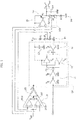
Figure 1 is a circuit diagram exemplifying possible embodiments, -
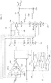
Figure 2 is another circuit diagram exemplifying possible embodiments, and -
Figure 3 is yet another circuit diagram exemplifying possible embodiments. - In the description that follows, one or more specific details are illustrated with the aim of providing an in-depth understanding of the examples of the embodiments of this description. The embodiments can be obtained without one or more of the specific details, or using other methods, components, materials, etc. In other cases, operations, materials or known structures are not illustrated or described in detail such that certain aspects of the embodiments will be made clear.
- Reference to "one embodiment" within the framework of the present description is intended to indicate that a particular configuration, structure or characteristic described with reference to the embodiment is included in at least one embodiment. Therefore, phrases like "in one embodiment" which can be present in one or more points of the present description do not necessarily refer specifically to the same embodiment. Furthermore, particular shapes, structures or characteristics can be combined in any suitable manner in one or more embodiments.
- The references used here are provided simply for convenience and therefore do not define the scope of protection or the importance of the embodiments.
- As has already been mentioned, charge pumps have formed the subject of widespread activities of study and innovation, from elementary solutions such as the one known in the literature as a "Two-Phase Voltage Doubler", or TPVD (with the charge accumulated in successive phases on a first and a second capacitor used to "pump" the charge onto an output capacitor), to more sophisticated solutions such as, for example, the one described in
US 5 874 850 A . - In this solution, if the charge pump is used to drive circuits which do not absorb current, the output voltage is double the input voltage. If instead the circuit driven by the charge pump absorbs a current level different from zero and increasing, then the output voltage of the charge pump tends to reduce with a ripple due to the switching of the two operating phases superimposed on the output voltage.
- These solutions are examples of open-loop solutions, in which the input voltage is not adjusted so as to hold the output voltage constant independently of the current absorbed by the circuit driven by the charge pump.
- Other charge pump solutions are described in documents such as
US 7 764 525 B2 ,US 2006/0181340 A1 orUS 2016/0181913 A1 . - These solutions insert the charge pump in a feedback loop, i.e. they are closed-loop solutions, with the feedback circuit which can modify the reference signal of the charge pump aiming to make sure that the average value of the output of the charge pump is constant independently of the current level absorbed by the circuit connected as load.
- With a determined load current value fixed, the ripple caused by the switching (at the frequency fCLK ) can be reduced (only) by increasing the output capacitance. At least in principle, in low-noise applications, in which it is desired to reduce this ripple as far as possible, consideration could be given to reducing the ripple to the desired level by suitably increasing the value of the output capacitance.
- This value can however not be realizable or require the occupation of an area (and therefore a cost) that is incompatible with the application demands or usage demands.
- In one or more embodiments, provision can be made to insert a charge pump in an implementation circuit, as exemplified in the figures, where the reference CP indicates a charge pump.
- For example, this can be, in one or more embodiments as exemplified in
Figure 1 , a charge pump with multiplication by 2. - In one or more embodiments, to realize the pump CP, it is possible to adopt various circuit diagrams, to be considered as known per se (see, for example, the documents mentioned previously), which makes it unnecessary to provide a description here in greater detail.
- By way of summary, for example a charge pump circuit can be considered, as exemplified in
Figure 1 , in which two first capacitors C1 are charged from a voltage VR (capable of being obtained for example from a reference voltage VREF by means of a differential input stage 10) throughrespective inverter stages 11 clocked by a clock signal CLK and with asecond inverter stage 12 which "pumps" the charge on the capacitors C1 onto a second capacitor C2, across which there is a voltage VCP multiplied by 2 with respect to the input VR. - Reference to such a circuit is of course purely exemplary and non-limiting in nature for the embodiments.
- One or more embodiments can in fact use charge pump circuits of different types, this being applicable also to the charge pumps CP exemplified in
Figures 2 and3 (which will be returned to later), which, instead of being charge pumps with multiplication by 2, can be charge pumps - of a type that are known per se - with multiplication by N, comprising, for example, a cascade of N-1 stages of the type described above by way of summary. - In one or more embodiments, the overall output of the circuit at the voltage VOUT (which it is desired to be equal, for example, to 2 times VREF -
Figure 1 - or to N times VREF -Figures 2 and3 ) can be provided on an output capacitor COUT with the provision - between the output of the charge pump CP at the voltage VCP and the overall output of the circuit at the voltage VOUT - of a circuit configuration capable of realizing two feedback control loops and substantially comparable to a low dropout (LDO) configuration. - In one or more embodiments, the first feedback loop can comprise a (first)
resistive voltage divider 14 comprising a plurality of resistors connected in series between the output of the charge pump CP on which the voltage VCP is present and ground GND, with an overall value of resistance equal to N times R1, where N represents the multiplication value of the charge pump CP (equal to 2 in the case ofFigure 1 , and N in the case ofFigures 2 and3 ). - In one or more embodiments, as exemplified in the figures (and referring to the more general case of
Figures 2 and3 , with the multiplication factor of the charge pump CP equal to N), thedivider 14 can ideally be seen as comprising N resistors with resistance value R1, one of which (for example the one connected to ground) is divided into two portions with resistance values equal to R1 - ΔR1 and ΔR1 respectively. - A voltage approximately equal to a submultiple N of VCP (i.e. equal to 1/N times VCP) can be detected across the resistance R1 - ΔR1 and brought back as input - according to methods discussed hereinafter - to the
differential stage 10 which generates VR from VREF. Referring to a voltage as "approximately" equal to a submultiple N of VCP takes into account the effect of the deviation with respect to R1 given by ΔR1. - In one or more embodiments, provision can be made for a second feedback control loop capable of acting so as to maintain a fixed difference ΔV between the voltage VCP and the voltage VOUT. For example (with reference to the polarities of the signals and of the components considered by way of example in the figures), the second feedback control loop can act so as to maintain the voltage VCP at a higher value, for example by an amount ΔV with respect to the voltage VOUT, so as to facilitate the correct operation of an output transistor (for example, MOS) 16a.
- In one or more embodiments, the
transistor 16a can be positioned: - with its current path (for example, source-drain, in the case of a field-effect transistor such as a MOSFET) between the output of the charge pump CP at the voltage VCP and the overall output voltage VOUT of the circuit, and
- the control terminal (for example, gate, in the case of a field-effect transistor such as a MOSFET) coupled to the output of a
differential stage 16b (for example, an operational amplifier) which senses, between its inverting and non-inverting inputs, the difference between the reference voltage VREF and a voltage equal to 1/N times VOUT where N represents the multiplication value of the charge pump CP (equal to 2 in the case ofFigure 1 , and N in the case ofFigures 2 and3 ) . - In one or more embodiments, the abovesaid voltage equal to 1/N times VOUT can be obtained by means of a
resistive divider 16c similar overall to thedivider 14 already described previously. - For example, in one or more embodiments, as exemplified in the figures (and referring again to the more general case of
Figures 2 and3 , with the multiplication factor of the charge pump CP equal to N), thedivider 16c can ideally be seen as comprising N resistors with resistance value R2, one of which (for example the second from the one connected to ground) is divided into two portions with resistance values equal to R2 - ΔR2 and ΔR2 respectively. - A voltage equal to a submultiple N of VOUT (i.e. equal to 1/N times VOUT) can be detected across the resistor of value R2 connected to ground GND and brought to the input (for example, non-inverting) of the
differential stage 16b. - At the same time, a voltage approximately equal to a submultiple N of VOUT (i.e. equal to 1/N times VOUT) can be detected on the resistance R2 + ΔR2 and brought back as input - also here according to methods discussed later - to the
differential stage 10 which generates VR from VREF. Again referring here to a voltage as "approximately" equal to a submultiple N of VCP takes into account the effect of the deviation with respect to R2 given by ΔR2. - In one or more embodiments, the attenuation of the ripple of the closed-loop charge pump configuration can be facilitated not only by virtue of the filtering effect of the output capacitance COUT, but also by virtue of the attenuating effect of the "Power Supply Rejection Ratio" (PSRR) of the LDO type circuit configuration described previously.
- In one or more embodiments, the additional attenuation being derived from the PSRR contribution can be added to the filtering effect of the capacitance COUT, with the advantage of being able to strongly attenuate the ripple signal even by using reduced values of the output capacitance COUT.
- In one or more embodiments, a high value can be chosen for the resistances R1 and R2, so as to reduce the current consumption of the
resistive dividers - In one or more embodiments, provision can be made for the
differential stage 10 which generates VR from VREF to comprise twodifferential pairs - the voltage "tapped" on the
divider 14 via the resistance of value R1 - ΔR1 connected to ground GND, - the voltage "tapped" on the
divider 16c via the resistance of value R2 + ΔR2 given by the series connection of the resistor of value R2 connected to ground GND (to which there is also coupled thedifferential stage 16b which drives thetransistor 16a) and the resistor of value ΔR2. - In one or more embodiments, the outputs of the two
differential circuits gain stage 103. - In one or more embodiments (in the case of the pump CP with multiplication by 2 exemplified in
Figure 1 ), it is possible to dimension the value of ΔR1 and ΔR2 (i.e. of the two "deviations" of the resistive values with respect to the values R1 and R2 linked to the multiplication factor of the charge pump CP) as follows:
- The combined effect of the two control loops described previously can then be expressed (in the case exemplified in
Figure 1 ) by the following relationships:
differential stage 10 and the second by the action of theamplifier 16b and of thetransistor 16a. - This is all with the voltage VCP maintained (for example, higher) at a level of difference ΔV with respect to the voltage VOUT, thus ensuring the correct operation of the
output transistor 16a (for example, with ΔV greater than or equal to the saturation source-drain voltage VSDsat of thetransistor 16a). - In one or more embodiments (in the more general case of the pump CP with multiplication by N exemplified in
Figures 2 and3 ), it is possible to dimension ΔR1 and ΔR2 as follows:
Figures 2 and3 ) by the following relationships:
differential stage 10 and the second by the action of theamplifier 16b and of thetransistor 16a and with the voltage VCP maintained (for example, higher) at a level of difference ΔV with respect to the voltage VOUT, thus ensuring the correct operation of theoutput transistor 16a (for example with ΔV greater than or equal to the saturation source-drain voltage VSDsat of thetransistor 16a). - In one or more embodiments, it is likewise possible to realize the
operational amplifier 16b of the LDO configuration such that the absorption of current by the output of the charge pump CP (at the voltage VCP) is minimum. -
Figure 3 exemplifies (with reference to the diagram ofFigure 2 , but this possibility applies also to the diagram ofFigure 1 ) the possibility, in one or more embodiments, of: - providing a switching
edge filtering unit 20 sensitive to the clock signal CLK of the charge pump CP, and - dividing the output capacitance COUT into two parts, indicated respectively by α.COUT and (1-α).COUT separated by a switch S1 driven by a sampling signal capable of being generated by the
unit 20. - In one or more embodiments, the insertion of the
unit 20 enables a further reduction of the ripple superimposed on the output signal at the clock frequency fCLK. - In one or more embodiments, the value of the division factor α can be chosen (for example, as a function of the application context and usage context) to be the value (between 0 and 1) which minimizes the abovesaid ripple.
- In one or more embodiments, the
unit 20 can "read" the clock signal CLK of the charge pump and generate the signal which drives the switch S1 which divides the output capacitance COUT into two. - For example, in one or more embodiments, the
unit 20 can comprise: - an
input line 200 which receives the signal CLK, sending it to alogic inverter 201 and to one of the inputs of a NORgate 202; - a
delay 203 of duration TD on the output of the NORgate 202; - a further NOR
gate 204 which receives as input the output of theinverter 201 and the output of thedelay 203; - a
further delay 205 of duration TD on the output of the NORgate 204, the output of which is sent back to the other input of the NORgate 202 and to one of the inputs of yet another NORgate 206 which receives on its other input the output of thedelay 203 and in turn provides as output the signal for driving the switch S1. - In one or more embodiments, the
unit 20 can therefore open the switch S1 for a brief time interval at the switching edge of the clock signal CLK, thus reducing the propagation of the ripple signal at the output. - Although exemplified here with reference to the circuits of
Figures 1 and2 , in one or more embodiments the solution referred to inFigure 3 (unit 20 which drives the switch S1 acting between the two parts of the output capacitance) can also be used alone, therefore also together with conventional type charge pump topologies. - When used in combination with circuits as exemplified in
Figures 1 and2 , the filtering effect of this solution will add to the filtering action on the ripple that can be produced by the PSRR of the output stage of these circuits, facilitating a further improvement of the ripple signal rejection performance. - In one or more embodiments used, for example, to drive switched capacitor circuits, it could be observed that the transient response after a current spike at the output is dictated primarily by the free-running operation of the charge pump without affecting the noise performance of the capacitors with the residual ripple at the sampling intervals duly reduced.
- Under these conditions of reduced residual ripple at the sampling intervals, it is possible to take advantage of the free-running operation (i.e. in the absence of frequency modulation phenomena of the charge pump which are induced by load current demands), with a resultant reduction in current consumption.
- One or more embodiments can therefore relate to a circuit comprising:
- a charge pump (for example, CP) with an input voltage (VR) and an output voltage (VCP) which is a multiple N (for example, equal to 2 in
Figure 1 , and equal in general to N inFigures 2 and3 ) of the input voltage, the charge pump having a clock input (for example, CLK), - an input stage (for example 10) with a reference terminal for receiving a reference voltage (VREF) and an output terminal coupled to the charge pump (CP) for applying the input voltage to the charge pump,
- at least one output capacitance (for example, COUT) coupled (for example, in 14, 16) to the charge pump and chargeable to an output voltage (VOUT) of the circuit,
- a feedback network comprising a first feedback loop (for example, 14) for feeding back the output voltage of the charge pump towards the input of the input stage and a second feedback loop (for example, 16a, 16b, 16c) for maintaining a fixed offset between the output voltage of the charge pump and the output voltage of the circuit, and/or
- said output capacitance being divided between two output capacitors (for example, α.COUT; (I-α).COUT) with a switch (for example, S1) set between the two output capacitors and with a driver unit (for example, 20) for driving the switch coupled to the clock input of the charge pump, the switch being openable (i.e. capable of being made non-conductive, uncoupling the two output capacitors from each other) by the driver unit at switching edges of the clock signal at the clock input of the charge pump.
- In one or more embodiments, said second feedback loop can comprise a transistor (for example, 16a) positioned with its current path (for example, source-drain if the transistor is a FET such as a MOSFET) between the output of the charge pump and the output capacitance.
- In one or more embodiments, said transistor can have a control terminal (for example, a gate, if the transistor is a FET such as a MOSFET) driven by a differential stage (for example, 16b) sensitive to the reference voltage on the reference terminal of the input stage and to a submultiple equal to said multiple N (i.e. VOUT/N) of the output voltage of the circuit.
- One or more embodiments can comprise a voltage divider (for example, 16c) between the output capacitance and said differential stage, said voltage divider having a division ratio (i.e. by which value the output of the divider is divided with respect to the input of the divider) equal to said multiple N.
- In one or more embodiments, the input stage can comprise:
- a first feedback input (for example, 101a) coupled to the output of the charge pump,
- a second feedback input (for example, 101b) coupled to the output capacitance, and
- a summing node (for example, 102) coupled to said first and second feedback input in such a way that the input voltage applied by the input stage to the charge pump is a function (for example, by means of the stage 103) of the feedback signals on said first and second feedback input of the input stage.
- One or more embodiments can comprise:
- a first voltage divider (for example, 14) between the output of the charge pump and the first feedback input of the input stage, and
- a second voltage divider (for example, 16c) between the output capacitance and the second feedback input of the input stage (10).
- In one or more embodiments, said first and second voltage divider can have respective division ratios (i.e. by which values the output of the divider is divided with respect to the input of the divider) with deviations of opposite sign (for example, the deviations or offsets -ΔR1, +ΔR2 with respect to R1 and R2) with respect to said multiple N.
- One or more embodiments can comprise a voltage divider (for example, the
divider 16c) coupled to the output capacitance and having a first tap point (for example, R2) towards said differential stage (for example, 16b) and a second tap point (for example, R2 + ΔR2) towards the second feedback input (101b) of the input stage. - In one or more embodiments, an electronic device (for example, a sensor) can comprise a charge pump circuit according to any of the preceding claims.
- One or more embodiments can relate to a method comprising providing a circuit with:
- a charge pump with an input voltage and an output voltage which is a multiple N of the input voltage, the charge pump having a clock input,
- an input stage with a reference terminal for receiving a reference voltage and an output terminal coupled to the charge pump for applying the input voltage to the charge pump,
- at least one output capacitance coupled to the charge pump and chargeable to an output voltage of the circuit,
- providing a first feedback of the output voltage of the charge pump towards the input of the input stage and a second feedback for maintaining a fixed offset between the output voltage of the charge pump and the output voltage of the circuit, and/or
- dividing said output capacitance between two output capacitors with a switch interposed between the two output capacitors, opening the switch at switching edges of the clock signal at the clock input of the charge pump.
- The underlying principles remaining the same, the details of construction and forms of embodiment may be varied, even significantly, with respect to those illustrated here purely by way of non-limiting example, without thereby departing from the scope of protection.
- Such scope of protection is defined by the accompanying claims.
Claims (10)
- A circuit comprising:- a charge pump (CP) with an input voltage (VR) and an output voltage (VCP) which is a multiple N of the input voltage (VR), the charge pump (CP) having a clock input (CLK),- an input stage (10) with a reference terminal for receiving a reference voltage (VREF) and an output terminal coupled to the charge pump (CP) for applying the input voltage (VR) to the charge pump (CP),- at least one output capacitance (COUT) coupled (14, 16) to the charge pump (CP) and chargeable to an output voltage (VOUT) of the circuit,the circuit comprising:- a feedback network (14, 16) comprising a first feedback loop (14) for feeding back the output voltage (VCP) of the charge pump (CP) towards the input of the input stage (10) and a second feedback loop (16a, 16b, 16c) for maintaining a fixed offset between the output voltage (VCP) of the charge pump (CP) and the output voltage (VOUT) of the circuit, and/or- said output capacitance (COUT) being divided between two output capacitors (α.COUT; (I-α).COUT), with a switch (S1) set between the two output capacitors and with a driver unit (20) for driving the switch (S1) coupled to the clock input (CLK) of the charge pump (CP), the switch (S1) being openable by the driver unit (20) at switching edges of the clock signal (CLK) at the clock input (CLK) of the charge pump (CP).
- The circuit according to Claim 1, with said second feedback loop (16) comprising a transistor (16a) positioned with its current path between the output of the charge pump (CP) and the output capacitance (COUT).
- The circuit according to Claim 2, wherein said transistor (16a) has a control terminal driven by a differential stage (16b) sensitive to the reference voltage (VREF) on the reference terminal of the input stage (10) and to a submultiple equal to said multiple N of the output voltage (VOUT) of the circuit.
- The circuit according to Claim 3, comprising a voltage divider (16c) between the output capacitance (COUT) and said differential stage (16b), said voltage divider having a division ratio equal to said multiple N.
- The circuit according to any of the preceding claims, wherein the input stage (10) comprises:- a first feedback input (101a) coupled to the output (VCP) of the charge pump (CP),- a second feedback input (101b) coupled to the output capacitance (COUT), and- a summing node (102) coupled to said first (101a) and second (101b) feedback input in such a way that the input voltage (VR) applied by the input stage to the charge pump (CP) is a function (103) of the feedback signals on said first (101a) and second (101b) feedback input of the input stage (10).
- The circuit according to Claim 5, comprising:- a first voltage divider (14) between the output (VCP) of the charge pump (CP) and the first feedback input (101a) of the input stage (10), and- a second voltage divider (16c) between the output capacitance (COUT) and the second feedback input (101b) of the input stage (10).
- The circuit according to Claim 6, wherein said first (14) and second (16c) voltage divider have respective division ratios with deviations of opposite sign (-ΔR1, +ΔR2) with respect to said multiple N.
- The circuit according to Claim 4 in combination with any of Claims 5 to 7, comprising a voltage divider (16c) coupled to the output capacitance (COUT) and having a first tap point (R2) towards said differential stage (16b) and a second tap point (R2 + ΔR2) towards the second feedback input (101b) of the input stage (10) .
- An electronic device comprising a charge pump circuit (10, CP, 14, 16) according to any of the preceding claims.
- A method comprising providing a circuit with:- a charge pump (CP) with an input voltage (VR) and an output voltage (VCP) which is a multiple N of the input voltage (VR), the charge pump (CP) having a clock input (CLK),- an input stage (10) with a reference terminal for receiving a reference voltage (VREF) and an output terminal coupled to the charge pump (CP) for applying the input voltage (VR) to the charge pump (CP),- at least one output capacitance (COUT) coupled (14, 16) to the charge pump (CP) and chargeable to an output voltage (VOUT) of the circuit,the method comprising:- providing a first feedback (14) of the output voltage (VCP) of the charge pump (CP) towards the input of the input stage (10) and a second feedback (16a, 16b, 16c) for maintaining a fixed offset between the output voltage (VCP) of the charge pump (CP) and the output voltage (VOUT) of the circuit, and/or- dividing said output capacitance (COUT) between two output capacitors (α.COUT; (I-α).COUT), with a switch (S1) interposed between the two output capacitors, opening the switch at switching edges of the clock signal (CLK) at the clock input (CLK) of the charge pump (CP).
Applications Claiming Priority (1)
| Application Number | Priority Date | Filing Date | Title |
|---|---|---|---|
| IT102017000007428A IT201700007428A1 (en) | 2017-01-24 | 2017-01-24 | CORRESPONDENT LOADING PUMP CIRCUIT, DEVICE AND PROCEDURE |
Publications (2)
| Publication Number | Publication Date |
|---|---|
| EP3352355A1 true EP3352355A1 (en) | 2018-07-25 |
| EP3352355B1 EP3352355B1 (en) | 2020-03-11 |
Family
ID=58737777
Family Applications (1)
| Application Number | Title | Priority Date | Filing Date |
|---|---|---|---|
| EP17190831.2A Active EP3352355B1 (en) | 2017-01-24 | 2017-09-13 | A charge pump circuit, corresponding device and method |
Country Status (4)
| Country | Link |
|---|---|
| US (1) | US10848058B2 (en) |
| EP (1) | EP3352355B1 (en) |
| CN (2) | CN108347162B (en) |
| IT (1) | IT201700007428A1 (en) |
Families Citing this family (4)
| Publication number | Priority date | Publication date | Assignee | Title |
|---|---|---|---|---|
| CN111917293B (en) * | 2020-06-22 | 2021-06-22 | 东南大学 | A Switched Capacitor DC-DC Converter with Multi-Voltage Domain Compound Feedback Mode |
| US11646658B2 (en) * | 2020-11-25 | 2023-05-09 | Stmicroelectronics S.R.L. | Charge pump circuit, corresponding device and method |
| US12216485B2 (en) * | 2021-07-08 | 2025-02-04 | Novatek Microelectronics Corp. | Output circuit and related control method with pumping compensation |
| IT202300011052A1 (en) * | 2023-05-31 | 2024-12-01 | St Microelectronics Int Nv | Digital temperature sensor, corresponding device and procedure |
Citations (7)
| Publication number | Priority date | Publication date | Assignee | Title |
|---|---|---|---|---|
| US5874850A (en) | 1994-08-12 | 1999-02-23 | Stmicroelectronics S.R.L. | Mos voltage elevator of the charge pump type |
| US20020034082A1 (en) * | 2000-09-19 | 2002-03-21 | Ichiro Yokomizo | DC / DC converter |
| US20060181340A1 (en) | 2005-02-17 | 2006-08-17 | Zywyn Corporation | Regulating charge pump |
| US7764525B2 (en) | 2008-03-24 | 2010-07-27 | Novatek Microelectronics Corp. | Apparatus of dynamic feedback control charge pump |
| US20140167713A1 (en) * | 2012-12-18 | 2014-06-19 | SK Hynix Inc. | Regulator and voltage generator |
| US20150192943A1 (en) * | 2014-01-09 | 2015-07-09 | Qualcomm Incorporated | Charge sharing linear voltage regulator |
| US20160181913A1 (en) | 2014-07-18 | 2016-06-23 | Guoyou Feng | Negative Charge Pump Feedback Circuit |
Family Cites Families (8)
| Publication number | Priority date | Publication date | Assignee | Title |
|---|---|---|---|---|
| EP0846996B1 (en) * | 1996-12-05 | 2003-03-26 | STMicroelectronics S.r.l. | Power transistor control circuit for a voltage regulator |
| ITMI20031924A1 (en) | 2003-10-07 | 2005-04-08 | Atmel Corp | HIGH PRECISION DIGITAL TO ANALOGUE CONVERTER WITH OPTIMIZED ENERGY CONSUMPTION. |
| US7554311B2 (en) * | 2006-07-31 | 2009-06-30 | Sandisk Corporation | Hybrid charge pump regulation |
| EP2065780B1 (en) * | 2007-11-30 | 2016-12-28 | ams AG | Controlled charge pump arrangement and method of controlling a clocked charge pump |
| US7944277B1 (en) * | 2008-01-04 | 2011-05-17 | Marvell International Ltd. | Circuit and methods of adaptive charge-pump regulation |
| CN102005917B (en) * | 2010-12-15 | 2012-11-14 | 电子科技大学 | Constant voltage output charge pump circuit |
| KR102021415B1 (en) * | 2012-12-14 | 2019-09-16 | 에스케이하이닉스 주식회사 | Voltage generator circuit |
| CN105915046B (en) * | 2016-04-27 | 2018-08-28 | 二十一世纪(北京)微电子技术有限公司 | A kind of control electrical appliances for electric charge pump |
-
2017
- 2017-01-24 IT IT102017000007428A patent/IT201700007428A1/en unknown
- 2017-09-13 EP EP17190831.2A patent/EP3352355B1/en active Active
- 2017-09-19 CN CN201710847537.5A patent/CN108347162B/en active Active
- 2017-09-19 CN CN201721201316.2U patent/CN207304376U/en not_active Withdrawn - After Issue
- 2017-10-30 US US15/797,643 patent/US10848058B2/en active Active
Patent Citations (7)
| Publication number | Priority date | Publication date | Assignee | Title |
|---|---|---|---|---|
| US5874850A (en) | 1994-08-12 | 1999-02-23 | Stmicroelectronics S.R.L. | Mos voltage elevator of the charge pump type |
| US20020034082A1 (en) * | 2000-09-19 | 2002-03-21 | Ichiro Yokomizo | DC / DC converter |
| US20060181340A1 (en) | 2005-02-17 | 2006-08-17 | Zywyn Corporation | Regulating charge pump |
| US7764525B2 (en) | 2008-03-24 | 2010-07-27 | Novatek Microelectronics Corp. | Apparatus of dynamic feedback control charge pump |
| US20140167713A1 (en) * | 2012-12-18 | 2014-06-19 | SK Hynix Inc. | Regulator and voltage generator |
| US20150192943A1 (en) * | 2014-01-09 | 2015-07-09 | Qualcomm Incorporated | Charge sharing linear voltage regulator |
| US20160181913A1 (en) | 2014-07-18 | 2016-06-23 | Guoyou Feng | Negative Charge Pump Feedback Circuit |
Also Published As
| Publication number | Publication date |
|---|---|
| CN108347162B (en) | 2020-09-15 |
| US10848058B2 (en) | 2020-11-24 |
| IT201700007428A1 (en) | 2018-07-24 |
| CN108347162A (en) | 2018-07-31 |
| CN207304376U (en) | 2018-05-01 |
| EP3352355B1 (en) | 2020-03-11 |
| US20180212514A1 (en) | 2018-07-26 |
Similar Documents
| Publication | Publication Date | Title |
|---|---|---|
| US11444537B2 (en) | Power converters and compensation circuits thereof | |
| US10571945B2 (en) | Low power regulator circuits, systems and methods regarding the same | |
| EP3352355B1 (en) | A charge pump circuit, corresponding device and method | |
| US10438546B2 (en) | Circuit for removing residual image after power-off, method for driving same, and display apparatus | |
| US10038378B2 (en) | Device and method to stabilize a supply voltage | |
| JP6118809B2 (en) | Master-slave low noise charge pump circuit and method | |
| US20140266122A1 (en) | Apparatus and methods for transient compensation of switching power regulators | |
| US20150061786A1 (en) | Crystal oscillator circuit having low power consumption, low jitter and wide operating range | |
| US20170090494A1 (en) | Compensation network for a regulator circuit | |
| US8283907B1 (en) | Boost regulator with pulse frequency mode of operation having substantially constant percentage output ripple and frequency | |
| US11644854B2 (en) | LDO, MCU, fingerprint module and terminal device | |
| EP0846996B1 (en) | Power transistor control circuit for a voltage regulator | |
| US10333393B2 (en) | Embedded charge pump voltage regulator | |
| US8749301B2 (en) | Power management device and power management method of touchable control system | |
| US8188719B2 (en) | Voltage regulator | |
| US20250293604A1 (en) | Multi-phase voltage regulator system | |
| KR102047181B1 (en) | Low power voltage regulator | |
| US10320296B2 (en) | Multi-phase voltage regulator system | |
| US6744296B1 (en) | Circuits and methods for accurately setting a phase shift | |
| EP3832431B1 (en) | Boost generation circuit, related circuit and chip, and wearable device | |
| US10715121B2 (en) | Parameter-independent ramp signal generation | |
| US8378658B2 (en) | Load swtch for removing high frequency ripple, noise and/or spikes while providing power to subsystems | |
| US20160301301A1 (en) | Voltage supply circuits and controlling methods therefor |
Legal Events
| Date | Code | Title | Description |
|---|---|---|---|
| PUAI | Public reference made under article 153(3) epc to a published international application that has entered the european phase |
Free format text: ORIGINAL CODE: 0009012 |
|
| STAA | Information on the status of an ep patent application or granted ep patent |
Free format text: STATUS: THE APPLICATION HAS BEEN PUBLISHED |
|
| AK | Designated contracting states |
Kind code of ref document: A1 Designated state(s): AL AT BE BG CH CY CZ DE DK EE ES FI FR GB GR HR HU IE IS IT LI LT LU LV MC MK MT NL NO PL PT RO RS SE SI SK SM TR |
|
| AX | Request for extension of the european patent |
Extension state: BA ME |
|
| STAA | Information on the status of an ep patent application or granted ep patent |
Free format text: STATUS: REQUEST FOR EXAMINATION WAS MADE |
|
| 17P | Request for examination filed |
Effective date: 20190122 |
|
| RBV | Designated contracting states (corrected) |
Designated state(s): AL AT BE BG CH CY CZ DE DK EE ES FI FR GB GR HR HU IE IS IT LI LT LU LV MC MK MT NL NO PL PT RO RS SE SI SK SM TR |
|
| STAA | Information on the status of an ep patent application or granted ep patent |
Free format text: STATUS: EXAMINATION IS IN PROGRESS |
|
| 17Q | First examination report despatched |
Effective date: 20190625 |
|
| GRAP | Despatch of communication of intention to grant a patent |
Free format text: ORIGINAL CODE: EPIDOSNIGR1 |
|
| STAA | Information on the status of an ep patent application or granted ep patent |
Free format text: STATUS: GRANT OF PATENT IS INTENDED |
|
| INTG | Intention to grant announced |
Effective date: 20191016 |
|
| GRAS | Grant fee paid |
Free format text: ORIGINAL CODE: EPIDOSNIGR3 |
|
| GRAA | (expected) grant |
Free format text: ORIGINAL CODE: 0009210 |
|
| STAA | Information on the status of an ep patent application or granted ep patent |
Free format text: STATUS: THE PATENT HAS BEEN GRANTED |
|
| AK | Designated contracting states |
Kind code of ref document: B1 Designated state(s): AL AT BE BG CH CY CZ DE DK EE ES FI FR GB GR HR HU IE IS IT LI LT LU LV MC MK MT NL NO PL PT RO RS SE SI SK SM TR |
|
| REG | Reference to a national code |
Ref country code: GB Ref legal event code: FG4D |
|
| REG | Reference to a national code |
Ref country code: CH Ref legal event code: EP |
|
| REG | Reference to a national code |
Ref country code: AT Ref legal event code: REF Ref document number: 1244399 Country of ref document: AT Kind code of ref document: T Effective date: 20200315 |
|
| REG | Reference to a national code |
Ref country code: DE Ref legal event code: R096 Ref document number: 602017012841 Country of ref document: DE |
|
| REG | Reference to a national code |
Ref country code: IE Ref legal event code: FG4D |
|
| PG25 | Lapsed in a contracting state [announced via postgrant information from national office to epo] |
Ref country code: FI Free format text: LAPSE BECAUSE OF FAILURE TO SUBMIT A TRANSLATION OF THE DESCRIPTION OR TO PAY THE FEE WITHIN THE PRESCRIBED TIME-LIMIT Effective date: 20200311 Ref country code: NO Free format text: LAPSE BECAUSE OF FAILURE TO SUBMIT A TRANSLATION OF THE DESCRIPTION OR TO PAY THE FEE WITHIN THE PRESCRIBED TIME-LIMIT Effective date: 20200611 Ref country code: RS Free format text: LAPSE BECAUSE OF FAILURE TO SUBMIT A TRANSLATION OF THE DESCRIPTION OR TO PAY THE FEE WITHIN THE PRESCRIBED TIME-LIMIT Effective date: 20200311 |
|
| REG | Reference to a national code |
Ref country code: NL Ref legal event code: MP Effective date: 20200311 |
|
| PG25 | Lapsed in a contracting state [announced via postgrant information from national office to epo] |
Ref country code: LV Free format text: LAPSE BECAUSE OF FAILURE TO SUBMIT A TRANSLATION OF THE DESCRIPTION OR TO PAY THE FEE WITHIN THE PRESCRIBED TIME-LIMIT Effective date: 20200311 Ref country code: SE Free format text: LAPSE BECAUSE OF FAILURE TO SUBMIT A TRANSLATION OF THE DESCRIPTION OR TO PAY THE FEE WITHIN THE PRESCRIBED TIME-LIMIT Effective date: 20200311 Ref country code: HR Free format text: LAPSE BECAUSE OF FAILURE TO SUBMIT A TRANSLATION OF THE DESCRIPTION OR TO PAY THE FEE WITHIN THE PRESCRIBED TIME-LIMIT Effective date: 20200311 Ref country code: GR Free format text: LAPSE BECAUSE OF FAILURE TO SUBMIT A TRANSLATION OF THE DESCRIPTION OR TO PAY THE FEE WITHIN THE PRESCRIBED TIME-LIMIT Effective date: 20200612 Ref country code: BG Free format text: LAPSE BECAUSE OF FAILURE TO SUBMIT A TRANSLATION OF THE DESCRIPTION OR TO PAY THE FEE WITHIN THE PRESCRIBED TIME-LIMIT Effective date: 20200611 |
|
| REG | Reference to a national code |
Ref country code: LT Ref legal event code: MG4D |
|
| PG25 | Lapsed in a contracting state [announced via postgrant information from national office to epo] |
Ref country code: NL Free format text: LAPSE BECAUSE OF FAILURE TO SUBMIT A TRANSLATION OF THE DESCRIPTION OR TO PAY THE FEE WITHIN THE PRESCRIBED TIME-LIMIT Effective date: 20200311 |
|
| PG25 | Lapsed in a contracting state [announced via postgrant information from national office to epo] |
Ref country code: SM Free format text: LAPSE BECAUSE OF FAILURE TO SUBMIT A TRANSLATION OF THE DESCRIPTION OR TO PAY THE FEE WITHIN THE PRESCRIBED TIME-LIMIT Effective date: 20200311 Ref country code: EE Free format text: LAPSE BECAUSE OF FAILURE TO SUBMIT A TRANSLATION OF THE DESCRIPTION OR TO PAY THE FEE WITHIN THE PRESCRIBED TIME-LIMIT Effective date: 20200311 Ref country code: LT Free format text: LAPSE BECAUSE OF FAILURE TO SUBMIT A TRANSLATION OF THE DESCRIPTION OR TO PAY THE FEE WITHIN THE PRESCRIBED TIME-LIMIT Effective date: 20200311 Ref country code: RO Free format text: LAPSE BECAUSE OF FAILURE TO SUBMIT A TRANSLATION OF THE DESCRIPTION OR TO PAY THE FEE WITHIN THE PRESCRIBED TIME-LIMIT Effective date: 20200311 Ref country code: CZ Free format text: LAPSE BECAUSE OF FAILURE TO SUBMIT A TRANSLATION OF THE DESCRIPTION OR TO PAY THE FEE WITHIN THE PRESCRIBED TIME-LIMIT Effective date: 20200311 Ref country code: PT Free format text: LAPSE BECAUSE OF FAILURE TO SUBMIT A TRANSLATION OF THE DESCRIPTION OR TO PAY THE FEE WITHIN THE PRESCRIBED TIME-LIMIT Effective date: 20200805 Ref country code: SK Free format text: LAPSE BECAUSE OF FAILURE TO SUBMIT A TRANSLATION OF THE DESCRIPTION OR TO PAY THE FEE WITHIN THE PRESCRIBED TIME-LIMIT Effective date: 20200311 Ref country code: IS Free format text: LAPSE BECAUSE OF FAILURE TO SUBMIT A TRANSLATION OF THE DESCRIPTION OR TO PAY THE FEE WITHIN THE PRESCRIBED TIME-LIMIT Effective date: 20200711 |
|
| REG | Reference to a national code |
Ref country code: AT Ref legal event code: MK05 Ref document number: 1244399 Country of ref document: AT Kind code of ref document: T Effective date: 20200311 |
|
| REG | Reference to a national code |
Ref country code: DE Ref legal event code: R097 Ref document number: 602017012841 Country of ref document: DE |
|
| PLBE | No opposition filed within time limit |
Free format text: ORIGINAL CODE: 0009261 |
|
| STAA | Information on the status of an ep patent application or granted ep patent |
Free format text: STATUS: NO OPPOSITION FILED WITHIN TIME LIMIT |
|
| PG25 | Lapsed in a contracting state [announced via postgrant information from national office to epo] |
Ref country code: ES Free format text: LAPSE BECAUSE OF FAILURE TO SUBMIT A TRANSLATION OF THE DESCRIPTION OR TO PAY THE FEE WITHIN THE PRESCRIBED TIME-LIMIT Effective date: 20200311 Ref country code: AT Free format text: LAPSE BECAUSE OF FAILURE TO SUBMIT A TRANSLATION OF THE DESCRIPTION OR TO PAY THE FEE WITHIN THE PRESCRIBED TIME-LIMIT Effective date: 20200311 Ref country code: IT Free format text: LAPSE BECAUSE OF FAILURE TO SUBMIT A TRANSLATION OF THE DESCRIPTION OR TO PAY THE FEE WITHIN THE PRESCRIBED TIME-LIMIT Effective date: 20200311 Ref country code: DK Free format text: LAPSE BECAUSE OF FAILURE TO SUBMIT A TRANSLATION OF THE DESCRIPTION OR TO PAY THE FEE WITHIN THE PRESCRIBED TIME-LIMIT Effective date: 20200311 |
|
| 26N | No opposition filed |
Effective date: 20201214 |
|
| PG25 | Lapsed in a contracting state [announced via postgrant information from national office to epo] |
Ref country code: SI Free format text: LAPSE BECAUSE OF FAILURE TO SUBMIT A TRANSLATION OF THE DESCRIPTION OR TO PAY THE FEE WITHIN THE PRESCRIBED TIME-LIMIT Effective date: 20200311 Ref country code: PL Free format text: LAPSE BECAUSE OF FAILURE TO SUBMIT A TRANSLATION OF THE DESCRIPTION OR TO PAY THE FEE WITHIN THE PRESCRIBED TIME-LIMIT Effective date: 20200311 |
|
| REG | Reference to a national code |
Ref country code: CH Ref legal event code: PL |
|
| REG | Reference to a national code |
Ref country code: BE Ref legal event code: MM Effective date: 20200930 |
|
| PG25 | Lapsed in a contracting state [announced via postgrant information from national office to epo] |
Ref country code: LU Free format text: LAPSE BECAUSE OF NON-PAYMENT OF DUE FEES Effective date: 20200913 |
|
| PG25 | Lapsed in a contracting state [announced via postgrant information from national office to epo] |
Ref country code: FR Free format text: LAPSE BECAUSE OF NON-PAYMENT OF DUE FEES Effective date: 20200930 |
|
| PG25 | Lapsed in a contracting state [announced via postgrant information from national office to epo] |
Ref country code: BE Free format text: LAPSE BECAUSE OF NON-PAYMENT OF DUE FEES Effective date: 20200930 Ref country code: CH Free format text: LAPSE BECAUSE OF NON-PAYMENT OF DUE FEES Effective date: 20200930 Ref country code: LI Free format text: LAPSE BECAUSE OF NON-PAYMENT OF DUE FEES Effective date: 20200930 Ref country code: IE Free format text: LAPSE BECAUSE OF NON-PAYMENT OF DUE FEES Effective date: 20200913 |
|
| GBPC | Gb: european patent ceased through non-payment of renewal fee |
Effective date: 20210913 |
|
| PG25 | Lapsed in a contracting state [announced via postgrant information from national office to epo] |
Ref country code: TR Free format text: LAPSE BECAUSE OF FAILURE TO SUBMIT A TRANSLATION OF THE DESCRIPTION OR TO PAY THE FEE WITHIN THE PRESCRIBED TIME-LIMIT Effective date: 20200311 Ref country code: MT Free format text: LAPSE BECAUSE OF FAILURE TO SUBMIT A TRANSLATION OF THE DESCRIPTION OR TO PAY THE FEE WITHIN THE PRESCRIBED TIME-LIMIT Effective date: 20200311 Ref country code: CY Free format text: LAPSE BECAUSE OF FAILURE TO SUBMIT A TRANSLATION OF THE DESCRIPTION OR TO PAY THE FEE WITHIN THE PRESCRIBED TIME-LIMIT Effective date: 20200311 |
|
| PG25 | Lapsed in a contracting state [announced via postgrant information from national office to epo] |
Ref country code: MK Free format text: LAPSE BECAUSE OF FAILURE TO SUBMIT A TRANSLATION OF THE DESCRIPTION OR TO PAY THE FEE WITHIN THE PRESCRIBED TIME-LIMIT Effective date: 20200311 Ref country code: MC Free format text: LAPSE BECAUSE OF FAILURE TO SUBMIT A TRANSLATION OF THE DESCRIPTION OR TO PAY THE FEE WITHIN THE PRESCRIBED TIME-LIMIT Effective date: 20200311 Ref country code: AL Free format text: LAPSE BECAUSE OF FAILURE TO SUBMIT A TRANSLATION OF THE DESCRIPTION OR TO PAY THE FEE WITHIN THE PRESCRIBED TIME-LIMIT Effective date: 20200311 |
|
| PG25 | Lapsed in a contracting state [announced via postgrant information from national office to epo] |
Ref country code: GB Free format text: LAPSE BECAUSE OF NON-PAYMENT OF DUE FEES Effective date: 20210913 |
|
| PGFP | Annual fee paid to national office [announced via postgrant information from national office to epo] |
Ref country code: DE Payment date: 20250820 Year of fee payment: 9 |