EP3352229A1 - Sapphire substrate and nitride semiconductor light emitting device - Google Patents
Sapphire substrate and nitride semiconductor light emitting device Download PDFInfo
- Publication number
- EP3352229A1 EP3352229A1 EP18153527.9A EP18153527A EP3352229A1 EP 3352229 A1 EP3352229 A1 EP 3352229A1 EP 18153527 A EP18153527 A EP 18153527A EP 3352229 A1 EP3352229 A1 EP 3352229A1
- Authority
- EP
- European Patent Office
- Prior art keywords
- nitride semiconductor
- sapphire substrate
- projections
- projection
- etching
- Prior art date
- Legal status (The legal status is an assumption and is not a legal conclusion. Google has not performed a legal analysis and makes no representation as to the accuracy of the status listed.)
- Granted
Links
Images


Classifications
-
- H—ELECTRICITY
- H10—SEMICONDUCTOR DEVICES; ELECTRIC SOLID-STATE DEVICES NOT OTHERWISE PROVIDED FOR
- H10P—GENERIC PROCESSES OR APPARATUS FOR THE MANUFACTURE OR TREATMENT OF DEVICES COVERED BY CLASS H10
- H10P14/00—Formation of materials, e.g. in the shape of layers or pillars
- H10P14/20—Formation of materials, e.g. in the shape of layers or pillars of semiconductor materials
- H10P14/29—Formation of materials, e.g. in the shape of layers or pillars of semiconductor materials characterised by the substrates
- H10P14/2924—Structures
- H10P14/2925—Surface structures
-
- C—CHEMISTRY; METALLURGY
- C30—CRYSTAL GROWTH
- C30B—SINGLE-CRYSTAL GROWTH; UNIDIRECTIONAL SOLIDIFICATION OF EUTECTIC MATERIAL OR UNIDIRECTIONAL DEMIXING OF EUTECTOID MATERIAL; REFINING BY ZONE-MELTING OF MATERIAL; PRODUCTION OF A HOMOGENEOUS POLYCRYSTALLINE MATERIAL WITH DEFINED STRUCTURE; SINGLE CRYSTALS OR HOMOGENEOUS POLYCRYSTALLINE MATERIAL WITH DEFINED STRUCTURE; AFTER-TREATMENT OF SINGLE CRYSTALS OR A HOMOGENEOUS POLYCRYSTALLINE MATERIAL WITH DEFINED STRUCTURE; APPARATUS THEREFOR
- C30B25/00—Single-crystal growth by chemical reaction of reactive gases, e.g. chemical vapour-deposition growth
- C30B25/02—Epitaxial-layer growth
- C30B25/18—Epitaxial-layer growth characterised by the substrate
- C30B25/183—Epitaxial-layer growth characterised by the substrate being provided with a buffer layer, e.g. a lattice matching layer
-
- C—CHEMISTRY; METALLURGY
- C30—CRYSTAL GROWTH
- C30B—SINGLE-CRYSTAL GROWTH; UNIDIRECTIONAL SOLIDIFICATION OF EUTECTIC MATERIAL OR UNIDIRECTIONAL DEMIXING OF EUTECTOID MATERIAL; REFINING BY ZONE-MELTING OF MATERIAL; PRODUCTION OF A HOMOGENEOUS POLYCRYSTALLINE MATERIAL WITH DEFINED STRUCTURE; SINGLE CRYSTALS OR HOMOGENEOUS POLYCRYSTALLINE MATERIAL WITH DEFINED STRUCTURE; AFTER-TREATMENT OF SINGLE CRYSTALS OR A HOMOGENEOUS POLYCRYSTALLINE MATERIAL WITH DEFINED STRUCTURE; APPARATUS THEREFOR
- C30B25/00—Single-crystal growth by chemical reaction of reactive gases, e.g. chemical vapour-deposition growth
- C30B25/02—Epitaxial-layer growth
- C30B25/18—Epitaxial-layer growth characterised by the substrate
- C30B25/186—Epitaxial-layer growth characterised by the substrate being specially pre-treated by, e.g. chemical or physical means
-
- C—CHEMISTRY; METALLURGY
- C30—CRYSTAL GROWTH
- C30B—SINGLE-CRYSTAL GROWTH; UNIDIRECTIONAL SOLIDIFICATION OF EUTECTIC MATERIAL OR UNIDIRECTIONAL DEMIXING OF EUTECTOID MATERIAL; REFINING BY ZONE-MELTING OF MATERIAL; PRODUCTION OF A HOMOGENEOUS POLYCRYSTALLINE MATERIAL WITH DEFINED STRUCTURE; SINGLE CRYSTALS OR HOMOGENEOUS POLYCRYSTALLINE MATERIAL WITH DEFINED STRUCTURE; AFTER-TREATMENT OF SINGLE CRYSTALS OR A HOMOGENEOUS POLYCRYSTALLINE MATERIAL WITH DEFINED STRUCTURE; APPARATUS THEREFOR
- C30B29/00—Single crystals or homogeneous polycrystalline material with defined structure characterised by the material or by their shape
- C30B29/10—Inorganic compounds or compositions
- C30B29/40—AIIIBV compounds wherein A is B, Al, Ga, In or Tl and B is N, P, As, Sb or Bi
- C30B29/403—AIII-nitrides
-
- H—ELECTRICITY
- H10—SEMICONDUCTOR DEVICES; ELECTRIC SOLID-STATE DEVICES NOT OTHERWISE PROVIDED FOR
- H10H—INORGANIC LIGHT-EMITTING SEMICONDUCTOR DEVICES HAVING POTENTIAL BARRIERS
- H10H20/00—Individual inorganic light-emitting semiconductor devices having potential barriers, e.g. light-emitting diodes [LED]
- H10H20/80—Constructional details
- H10H20/81—Bodies
- H10H20/815—Bodies having stress relaxation structures, e.g. buffer layers
-
- H—ELECTRICITY
- H10—SEMICONDUCTOR DEVICES; ELECTRIC SOLID-STATE DEVICES NOT OTHERWISE PROVIDED FOR
- H10P—GENERIC PROCESSES OR APPARATUS FOR THE MANUFACTURE OR TREATMENT OF DEVICES COVERED BY CLASS H10
- H10P14/00—Formation of materials, e.g. in the shape of layers or pillars
- H10P14/20—Formation of materials, e.g. in the shape of layers or pillars of semiconductor materials
- H10P14/29—Formation of materials, e.g. in the shape of layers or pillars of semiconductor materials characterised by the substrates
- H10P14/2901—Materials
- H10P14/2921—Materials being crystalline insulating materials
-
- H—ELECTRICITY
- H10—SEMICONDUCTOR DEVICES; ELECTRIC SOLID-STATE DEVICES NOT OTHERWISE PROVIDED FOR
- H10P—GENERIC PROCESSES OR APPARATUS FOR THE MANUFACTURE OR TREATMENT OF DEVICES COVERED BY CLASS H10
- H10P14/00—Formation of materials, e.g. in the shape of layers or pillars
- H10P14/20—Formation of materials, e.g. in the shape of layers or pillars of semiconductor materials
- H10P14/34—Deposited materials, e.g. layers
- H10P14/3402—Deposited materials, e.g. layers characterised by the chemical composition
- H10P14/3414—Deposited materials, e.g. layers characterised by the chemical composition being group IIIA-VIA materials
- H10P14/3416—Nitrides
-
- H—ELECTRICITY
- H10—SEMICONDUCTOR DEVICES; ELECTRIC SOLID-STATE DEVICES NOT OTHERWISE PROVIDED FOR
- H10P—GENERIC PROCESSES OR APPARATUS FOR THE MANUFACTURE OR TREATMENT OF DEVICES COVERED BY CLASS H10
- H10P14/00—Formation of materials, e.g. in the shape of layers or pillars
- H10P14/20—Formation of materials, e.g. in the shape of layers or pillars of semiconductor materials
- H10P14/36—Formation of materials, e.g. in the shape of layers or pillars of semiconductor materials characterised by treatments done before the formation of the materials
-
- H—ELECTRICITY
- H10—SEMICONDUCTOR DEVICES; ELECTRIC SOLID-STATE DEVICES NOT OTHERWISE PROVIDED FOR
- H10H—INORGANIC LIGHT-EMITTING SEMICONDUCTOR DEVICES HAVING POTENTIAL BARRIERS
- H10H20/00—Individual inorganic light-emitting semiconductor devices having potential barriers, e.g. light-emitting diodes [LED]
- H10H20/80—Constructional details
- H10H20/81—Bodies
- H10H20/822—Materials of the light-emitting regions
- H10H20/824—Materials of the light-emitting regions comprising only Group III-V materials, e.g. GaP
- H10H20/825—Materials of the light-emitting regions comprising only Group III-V materials, e.g. GaP containing nitrogen, e.g. GaN
Definitions
- the present invention relates to a sapphire substrate for a nitride semiconductor light emitting device and a method for manufacturing the same, and a nitride semiconductor light emitting device incorporating the sapphire substrate.
- a light emitting diode (LED) made of a nitride semiconductor is usually constituted by sequentially laminating an n-type semiconductor layer, an active layer and a p-type semiconductor layer on a sapphire substrate.
- LED light emitting diode
- emitted light is extracted from the side opposite the sapphire substrate or the side of the sapphire substrate, while light emitted from the active layer is also radiated in a direction opposite the light emission side. Therefore, it becomes necessary to improve external quantum efficiency by enabling light radiated in a direction opposite the light emission side to be extracted effectively from the light emission side.
- Patent Document 1 discloses that external quantum efficiency is improved by arranging a plurality of truncated triangular pyramid-shaped projections on a sapphire substrate.
- JP-A-2008-177528 also describes that generation of voids and deterioration of crystallinity can be lessened by enabling crystal growth on a surface, on which truncated triangular pyramid-shaped projections are formed, through the projections.
- Patent Document 1 JP-A-2008-177528
- an object of the present invention is to provide a sapphire substrate for a nitride semiconductor light emitting device that enables the growth of a nitride semiconductor having more improved, possibly excellent crystallinity, and also can constitute a nitride semiconductor light emitting device having more improved, even excellent light extraction efficiency, and a method for manufacturing the same.
- Another object of the present invention is to provide a nitride semiconductor light emitting device that includes a nitride semiconductor having excellent crystallinity, and is also excellent in light extraction efficiency.
- the sapphire substrate according to the present invention is a sapphire substrate having one principal surface on which a nitride semiconductor is grown to form a nitride semiconductor light emitting device, said one principal surface having a plurality of projections.
- each of the projections has a pyramidal shape with a not truncated, more sharpened tip and with an inclined surface which is composed of a crystal growth-suppression surface that lessens or suppresses the growth of the nitride semiconductor in comparison with a substrate surface located between adjacent projections and also which has an inclination change line at which an inclination angle discontinuously varies.
- a bottom surface of each projection has a generally polygonal shape with outwardly bulged circular arc-shaped three or more sides, the inclined surface is composed of a plurality of generally triangular inclined surfaces including both ends of each side and the substantially sharpened tip as a vertex, and an inclination angle of each inclined surface discontinuously varies in the inclination change line.
- an inclination angle of the inclined surface above the inclination change line is preferably smaller than that of the inclined surface below the inclination change line.
- the projections are preferably located on one principal surface in a mutually separated state.
- the projections are periodically arranged on said one principal surface, preferably, and the projections are located on vertexes of a triangular lattice, a quadrangular lattice, or a hexagonal lattice as a periodical arrangement of the projection.
- a nitride semiconductor light emitting device comprises the sapphire substrate according to the present invention and a nitride semiconductor layer formed by growing a nitride semiconductor on said one principal surface of the sapphire.
- the method for manufacturing a sapphire substrate for a nitride semiconductor light emitting device is a method for manufacturing a sapphire substrate for a nitride semiconductor light emitting device, including:
- each of a plurality of projections formed on one principal surface has a pyramidal shape with a substantially sharpened tip
- each inclined surface of the projection is composed of a crystal growth-suppression surface that lessens or suppresses the growth of the nitride semiconductor in comparison with a substrate surface located between adjacent projections, and also has an inclination change line at which an inclination angle discontinuously varies
- the sapphire substrate enables the growth of a nitride semiconductor having improved or excellent crystallinity, and also can constitute a nitride semiconductor light emitting device having improved or excellent light extraction efficiency.
- the nitride semiconductor light emitting device is provided with a semiconductor laminated structure 2 in which a base layer 21, a first conductive layer (n-type layer) 22, an active layer (emissive layer) 23 and a second conductive layer (p-type layer) 24 are sequentially laminated on a sapphire substrate 10, and a plurality of projections (dimples) 1, each having a generally pyramidal shape with a substantially sharpened tip, are provided on a surface of the substrate 10 on which the base layer 21 is grown.
- a semiconductor laminated structure 2 in which a base layer 21, a first conductive layer (n-type layer) 22, an active layer (emissive layer) 23 and a second conductive layer (p-type layer) 24 are sequentially laminated on a sapphire substrate 10, and a plurality of projections (dimples) 1, each having a generally pyramidal shape with a substantially sharpened tip, are provided on a surface of the substrate 10 on which the base layer 21 is grown.
- the base layer 21, the first conductive layer (n-type layer) 22, the active layer (emissive layer) 23 and the second conductive layer (p-type layer) 24, each being made of a nitride semiconductor, are grown on a surface of the substrate 10 provided with a plurality of projections (dimple) 1, each having a generally pyramidal shape with a substantially sharpened tip, the semiconductor layers can be grown with satisfactory crystallinity.
- the semiconductor light emitting device of the embodiment it also becomes possible to efficiently reflect light emitted from the emissive layer 23 in the light emission direction by a plurality of projections 1, each having a generally pyramidal shape with a substantially sharpened tip, and thus light extraction efficiency can be enhanced.
- light that propagates in the transverse direction can be reflected and diffracted on projection 1, particularly an inclined surface of projection 1.
- the projection (dimple) 1 is formed into a generally triangular pyramid shape, as shown in Figs. 2(a) and 2(b) ,
- the inclined surfaces 11k, 12k and 13k are respectively bent at inclination change lines L11, L12 and L13, and the inclination at the side above inclination change lines L11, L12 and L13 (vertex side) is more gentle than the inclination at the side below inclination change lines (bottom surface side).
- the projection (dimple) 1 has a generally triangular pyramid shape and a vertex t1 thereof is substantially sharpened.
- a substantially sharpened vertex means that a vertex portion (top surface) of the projection 1 becomes smaller so that a nitride semiconductor does not grow from the vertex of the projection (dimple) 1.
- the projections 1 having a generally triangular pyramid shape of the present embodiment being discussed can be formed by setting the crystal form of a substrate, the plane direction of a substrate surface on which projection 1 are formed, the mask shape and size, and the etching conditions according to the objective shape.
- etching when a circular first mask is formed on a surface made of the C-plane of a sapphire substrate and etching is carried out, the portion on which no mask is formed is removed by etching to form a circular projection reflecting a mask shape faithfully in an initial stage.
- an influence of direction dependency of an etching rate an etching proceeding rate varies depending on a direction caused by a crystal form is exerted, resulting in a shape reflecting the crystal form.
- etching proceeds as a result of reflecting of the crystal form, and thus three vertices of a bottom portion and a ridge line of a triangular pyramid gradually become clear to form a lower projection 1a having a generally triangular pyramid-shape below a circular mask.
- a top surface of the lower projection 1a having a generally triangular pyramid-shape is etched in a generally triangular shape and the area becomes smaller than that of the circular mask by undercut.
- a bottom surface and a top surface of the lower projection 1a becomes a generally triangle shape in which the respective sides are outwardly bulged in a circular arc shape.
- the area becomes smaller and also a curvature radius of a circular arc of each side becomes larger, and thus each side becomes linear.
- a second mask is formed on a top surface of the lower projection 1a or etching is carried out without forming the second mask, thereby further forming an upper projection 1b having a triangular pyramid shape on the lower projection 1a to form a projection (dimple) 1 having a generally triangular pyramid shape, including inclined surfaces 11k, 12k and 13k in which inclination discontinuously varies at inclination change lines L11, L12 and L13 as the border.
- a projection 1 into a generally triangular pyramid shape in which the respective sides 11, 12 and 13 of a bottom surface are linear and inclined surfaces 11k, 12k and 13k are flat, and it is also possible to form a projection 1 into a generally triangular pyramid shape in which the respective sides 11, 12 and 13, and inclined surfaces 11k, 12k and 13k of a bottom surface have an inwardly curved circular arc-shape.
- projections 1 on the substrate enable an improvement in optical output and light extraction efficiency and, in case the base layer 21 is grown, inclined surfaces 11k, 12k and 13k of projection 1 serve as a surface of suppressing the growth of the base layer 21 (also referred to as a crystal growth-suppression surface) and enables promotion of the growth of a base layer grown from a surface between projections 1 (hereinafter referred to as a crystal growth surface) in a transverse direction to form the base layer 21 having a surface with less crystal defects. Accordingly, it is preferred that projections constituting the crystal growth-suppression surface are uniformly distributed in the crystal growth surface, and are regularly arranged in a mutually separated state as shown in Figs. 3 to 4 .
- Fig. 3 is a triangular lattice point arrangement
- Fig. 4 is a square lattice point arrangement.
- projections 1 on the substrate are preferably formed at a high density. In this manner, when projections 1 are arranged at a high density, a ratio of an area of the crystal growth-suppression surface to the crystal growth surface becomes higher.
- projections 1 of the present embodiment because the inclination at the side above inclination change lines L11, L12 and L13 (vertex side) is more gentle than that at the side below inclination change lines (bottom surface side) in the respective inclined surfaces 11k, 12k and 13k, the growth of a nitride semiconductor in the transverse direction is more promoted at inclination change lines L11, L12 and L13 as the border. In this way, a nitride semiconductor having more satisfactory crystallinity is formed and also flattening of a surface of the grown nitride semiconductor is promoted.
- regular and high-density arrangement of the projection 1 include, in addition to the triangular lattice point arrangement and the square lattice point arrangement as shown in Figs. 3 to 4 , arrangements such as a parallelogram lattice point arrangement and a rectangular lattice point arrangement.
- This regular structure may be arranged with the same regularity in the entire substrate surface, or may be arranged with the different regularity according to electrode arrangement of a semiconductor device structure formed on a substrate.
- the height of the projection 1 is set within a range of 0.5 ⁇ m or more and 2 ⁇ m or less, and preferably within a range of 0.7 ⁇ m or more and 1.2 ⁇ m or less, and the interval (interval of the narrowest portion) of projections 1 is set within a range of 0.5 ⁇ m or more and 2 ⁇ m or less, and preferably 1.5 ⁇ m or less.
- One side (a linear distance between vertices of a bottom surface) of the bottom surface of the projection 1 is set within a range of 0.5 ⁇ m or more and 3 ⁇ m or less, and preferably within a range of 0.7 ⁇ m or more and 2 ⁇ m or less.
- a projection 1 that includes a substantially sharpened vertex t1 and also includes inclined surfaces 11k, 12k and 13k composed of a crystal growth-suppression surface in which an inclination angle discontinuously varies above and below inclination change lines L11, L12 and L13, on a substrate 10, for example, by a two-stage etching described below.
- a circular first mask 19 is formed on the C-plane (0001) of a sapphire substrate 10 and, after etching a substrate, the first mask 19 is removed.
- a generally triangular pyramid-shaped lower projection 1a including a generally triangular top surface is formed ( Fig. 6 ).
- the etching method includes a wet etching method and a dry etching method, and any etching method may be used in the present invention. Specifically, a vapor phase etching method, a plasma etching method and a reactive ion etching method can be used as the dry etching method. Examples of an etching gas used in the case of etching include C1-based and F-based gases, for example, Cl 2 , SiCl 4 , BCl 3 , HBr, SF 6 , CHF 3 , C 4 F 8 , CF 4 , and an inert gas such as Ar.
- C1-based and F-based gases for example, Cl 2 , SiCl 4 , BCl 3 , HBr, SF 6 , CHF 3 , C 4 F 8 , CF 4 , and an inert gas such as Ar.
- silicon oxide such as SiO 2 can be appropriately selected as a mask material according to a substrate material and an etching solution therefor, and examples thereof include oxides of at least one element selected from the group consisting of V, Zr, Nb, Hf, Ti, Ta and Al, and nitrides of at least one element selected from the group consisting of Si, B and Al.
- a circular second mask 20 is formed on a top surface of the lower projection 1a, or the substrate 1 is further etched without forming the second mask 20.
- etching is allowed to proceed until at least an upper projection having a substantially sharpened tip is formed on the top surface of the lower projection.
- This etching method may be either a wet etching method or a dry etching method similar to the first etching step.
- the etching method an etching method that is different from that of the first etching step. That is, the wet etching method may be used in the first etching step and the drying etching method may be used in the second etching step, or the method may be alternated.
- the etching gas or etching solution may vary.
- a projection 1 that includes a substantially sharpened vertex t1 and also includes inclined surfaces 11k, 12k and 13k composed of a crystal growth-suppression surface in which an inclination angle discontinuously varies above and below inclination change lines L11, L12 and L13, on a substrate 10, for example, by the aforementioned two-stage etching described.
- the nitride semiconductor grown from the C-plane (0001) surface of sapphire between projections 1 grows on the inclined surface of the projection 1 in the transverse direction, and covers the projection 1 as the growth to obtain a flat GaN surface with less crystal defects, and thus it becomes possible to form, on the flat GaN surface with less crystal defects, a light emitting device structure in which a nitride semiconductor layer with less crystal defects has been laminated.
- a light emitting device structure includes, on a substrate, a laminated structure 2 including first and second conductive layers 22, 24 and an active layer 23 formed therebetween, and also includes a first electrode and a second electrode formed on the first conductive layer 22 and the second conductive layer 24 exposed by removing a portion of the active layer 23 and the second conductive layer 24.
- the second electrode includes a translucent ohmic electrode formed over nearly the entire surface of the second conductive layer 24, a pad formed on the translucent ohmic electrode, and a diffusion electrode.
- a gallium nitride-based compound semiconductor material represented by the general formula: In x Al y Ga 1-x-y N (0 ⁇ x ⁇ 1, 0 ⁇ y ⁇ 1, 0 ⁇ x + y ⁇ 1).
- binary and tertiary mixed crystals thereof can be used particularly suitably.
- other semiconductors such as GaAs- and GaP-based compound semiconductors, AlGaAs- and InAlGaP-based compound semiconductors.
- a SiO 2 film was formed, followed by patterning to periodically form a circular first mask 19 having a diameter of about 1.5 ⁇ m.
- the substrate was immersed in an etching bath using a mixed acid of phosphoric acid and sulfuric acid as an etching solution and etched at a solution temperature of about 290°C for about 5 minutes until the depth (projection height) becomes about 1 ⁇ m.
- the substrate was immersed in an etching bath using a mixed acid of phosphoric acid and sulfuric acid as an etching solution, in a state of absence of a mask, and etched at a solution temperature of about 290°C for about 1 minute until a tip of projection is substantially sharpened to form an upper projection 1b.
- a projection 1 having a height of about 1 ⁇ m and a two-stage taper angle was formed by the aforementioned steps.
- the substrate was transferred to a MOCVD device, where a 20 nm thick GaN buffer layer grown at a low temperature (about 510°C) was formed on a substrate surface with projection 1 formed thereon, and GaN was c-axis grown thereon at a high temperature (about 1,050°C) to form a base layer 21 having a flat surface.
- a MOCVD device where a 20 nm thick GaN buffer layer grown at a low temperature (about 510°C) was formed on a substrate surface with projection 1 formed thereon, and GaN was c-axis grown thereon at a high temperature (about 1,050°C) to form a base layer 21 having a flat surface.
- an n-type layer 22 such as an n-type contact layer, an active layer 23 and a p-type layer 24 were formed to manufacture a semiconductor device structure.
- an n-side contact layer having a film thickness of 5 ⁇ m made of Si (4.5 ⁇ 10 18 /cm 3 ) doped GaN, 0.3 ⁇ m thick undoped GaN layer, 0.03 ⁇ m thick Si (4.5 ⁇ 10 18 /cm 3 ) doped GaN layers, 5 nm thick undoped GaN layer, a multi-layered film obtained by repeatedly and alternately laminating each 10 layers of 4 nm thick undoped GaN layers and 2 nm thick undoped In 0.1 Ga 0.9 N layers are formed on the aforementioned base layer 21.
- a multiple quantum well structure obtained by repeatedly and alternately laminating each 6 layers of barrier layers having a film thickness of 25 nm made of undoped GaN and well layers having a film thickness of 3 nm made of In 0.3 Ga 0.7 Nnd finally laminating a barrier layer is formed on the n-type layer.
- a p-side multi-layered film layer which has a structure obtained by repeatedly and alternately laminating each 5 layers of 4 nm thick Mg (5 ⁇ 10 19 /cm 3 ) doped Al 0.15 Ga 0.85 N layers and 2.5 nm thick Mg (5 ⁇ 10 19 /cm 3 ) doped In 0.03 Ga 0.97 N layers; and finally laminating with the AlGaN layer formed thereon and a p-side contact layer having a film thickness 0.12 ⁇ m made of Mg (1 ⁇ 10 20 /cm 3 ) doped GaN are formed on the active layer. With this, a structure (emission wavelength of 465 nm, blue LED) can be obtained.
- the semiconductor device structure was provided with an electrode having a structure in which ITO (about 170 nm) is formed as a translucent ohmic electrode on a surface of a p-type layer 24, that would serve as a surface of an emitting structure portion, and then Rh (about 100 nm), Pt (about 200 nm) and Au (about 500 nm) are laminated in this order on ITO and the n-side contact layer.
- ITO about 170 nm
- Rh about 100 nm
- Pt about 200 nm
- Au about 500 nm
- Embodiment 1 A sapphire substrate having a principal surface on which a nitride semiconductor is grown to form a nitride semiconductor light emitting device, comprising a plurality of projections on the principal surface, wherein each of the projections has a generally pyramidal shape with a substantially sharpened tip and an inclined surface, the inclined surface being composed of a crystal growth-suppression surface that lessens the growth of the nitride semiconductor in comparison with a substrate surface located between adjacent projections, the inclined surface having an inclination change line at which an inclination angle discontinuously varies.
- Embodiment 2 The sapphire substrate according to the features of embodiment 1, wherein a bottom surface of the projection has a generally polygonal shape with outwardly bulged circular arc-shaped three or more sides, the inclined surface is composed of a plurality of generally triangular inclined surfaces each including both ends of each side and the substantially sharpened tip as a vertex, and an inclination angle of each inclined surface discontinuously varies in the inclination change line.
- Embodiment 3 The sapphire substrate according to the features of embodiment 1 or 2, wherein an inclination angle of the inclined surface above the inclination change line is smaller than that of the inclined surface below the inclination change line.
- Embodiment 4 The sapphire substrate as in one of embodiments 1 to 3, wherein the projections are located separately on the principal surface.
- Embodiment 5 The sapphire substrate as in one of embodiments 1 to 4, wherein the projections are periodically arranged on the principal surface.
- Embodiment 6 The sapphire substrate according to the features of embodiment 5, wherein the projections are located on vertexes of a triangular lattice, a quadrangular lattice or a hexagonal lattice.
- Embodiment 7 A nitride semiconductor light emitting device comprising: the sapphire substrate as in one of embodiments 1 to 6; and a nitride semiconductor layer formed by growing a nitride semiconductor on the principal surface of the sapphire.
- Embodiment 8 A method for manufacturing a sapphire substrate for a nitride semiconductor light emitting device, the method comprising:
- Embodiment 9 The method for manufacturing a sapphire substrate for a nitride semiconductor light emitting device according to the features of embodiment 8, further comprising a second mask forming step of forming second mask on upper surfaces of the lower projection between the first mask removing step and the second etching step.
Landscapes
- Chemical & Material Sciences (AREA)
- Engineering & Computer Science (AREA)
- Crystallography & Structural Chemistry (AREA)
- Materials Engineering (AREA)
- Metallurgy (AREA)
- Organic Chemistry (AREA)
- Chemical Kinetics & Catalysis (AREA)
- General Chemical & Material Sciences (AREA)
- Inorganic Chemistry (AREA)
- Led Devices (AREA)
Abstract
Description
- The present invention relates to a sapphire substrate for a nitride semiconductor light emitting device and a method for manufacturing the same, and a nitride semiconductor light emitting device incorporating the sapphire substrate.
- A light emitting diode (LED) made of a nitride semiconductor is usually constituted by sequentially laminating an n-type semiconductor layer, an active layer and a p-type semiconductor layer on a sapphire substrate. In this light emitting diode, emitted light is extracted from the side opposite the sapphire substrate or the side of the sapphire substrate, while light emitted from the active layer is also radiated in a direction opposite the light emission side. Therefore, it becomes necessary to improve external quantum efficiency by enabling light radiated in a direction opposite the light emission side to be extracted effectively from the light emission side.
- For example,
Patent Document 1 discloses that external quantum efficiency is improved by arranging a plurality of truncated triangular pyramid-shaped projections on a sapphire substrate.JP-A-2008-177528 - Patent Document 1:
JP-A-2008-177528 - However, the present inventors have intensively studied and found that crystallinity of a nitride semiconductor grown on a surface with truncated triangular pyramid-shaped dimples is not necessarily satisfactory.
- With the increase of the output of a light emitting diode, problems due to crystal defects, which have not arisen in prior light emitting diodes, have recently arisen.
- Thus, an object of the present invention is to provide a sapphire substrate for a nitride semiconductor light emitting device that enables the growth of a nitride semiconductor having more improved, possibly excellent crystallinity, and also can constitute a nitride semiconductor light emitting device having more improved, even excellent light extraction efficiency, and a method for manufacturing the same.
- Another object of the present invention is to provide a nitride semiconductor light emitting device that includes a nitride semiconductor having excellent crystallinity, and is also excellent in light extraction efficiency. Solution to Problem
- In order to try to achieve the aforementioned objects, the sapphire substrate according to the present invention is a sapphire substrate having one principal surface on which a nitride semiconductor is grown to form a nitride semiconductor light emitting device, said one principal surface having a plurality of projections. And each of the projections has a pyramidal shape with a not truncated, more sharpened tip and with an inclined surface which is composed of a crystal growth-suppression surface that lessens or suppresses the growth of the nitride semiconductor in comparison with a substrate surface located between adjacent projections and also which has an inclination change line at which an inclination angle discontinuously varies.
- In the sapphire substrate according to the present invention, a bottom surface of each projection has a generally polygonal shape with outwardly bulged circular arc-shaped three or more sides, the inclined surface is composed of a plurality of generally triangular inclined surfaces including both ends of each side and the substantially sharpened tip as a vertex, and an inclination angle of each inclined surface discontinuously varies in the inclination change line.
- In the sapphire substrate according to the present invention, regarding each inclined surface of the projection, an inclination angle of the inclined surface above the inclination change line is preferably smaller than that of the inclined surface below the inclination change line.
- In the sapphire substrate according to the present invention, the projections are preferably located on one principal surface in a mutually separated state.
- In the sapphire substrate according to the present invention, the projections are periodically arranged on said one principal surface, preferably, and the projections are located on vertexes of a triangular lattice, a quadrangular lattice, or a hexagonal lattice as a periodical arrangement of the projection.
- A nitride semiconductor light emitting device according to the present invention comprises the sapphire substrate according to the present invention and a nitride semiconductor layer formed by growing a nitride semiconductor on said one principal surface of the sapphire.
- The method for manufacturing a sapphire substrate for a nitride semiconductor light emitting device according to the present invention is a method for manufacturing a sapphire substrate for a nitride semiconductor light emitting device, including:
- a first etching step of forming a first mask on the C-plane of a sapphire substrate, and etching the sapphire substrate using the first mask as an etching mask to form a lower projection having a truncated pyramidal shape,
- a first mask removing step of removing the first mask thereby exposing a top surface of the lower projection, and
- a second etching step of further etching the lower projection whose top surface has been exposed to form an upper projection having a pyramidal shape with a substantially sharpened tip on the lower projection.
- In the sapphire substrate according to the present invention constituted as mentioned above, because each of a plurality of projections formed on one principal surface has a pyramidal shape with a substantially sharpened tip, and each inclined surface of the projection is composed of a crystal growth-suppression surface that lessens or suppresses the growth of the nitride semiconductor in comparison with a substrate surface located between adjacent projections, and also has an inclination change line at which an inclination angle discontinuously varies, the sapphire substrate enables the growth of a nitride semiconductor having improved or excellent crystallinity, and also can constitute a nitride semiconductor light emitting device having improved or excellent light extraction efficiency.
-
-
Fig. 1 is a sectional view of a nitride semiconductor light emitting device according to an embodiment of the present invention. -
Fig. 2(a) is a plan view of aprojection 1 in a nitride semiconductor light emitting device of the embodiment, andFig. 2(b) is a sectional view taken along lines A-A' ofFig. 2(a) . -
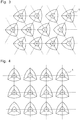
Fig. 3 is a plan view showing an example of an arrangement ofprojections 1 in a nitride semiconductor light emitting of the embodiment. -
Fig. 4 is a plan view showing another example of an arrangement ofprojections 1 in a nitride semiconductor light emitting of the embodiment. -
Fig. 5 is a plan view when afirst mask 19 for the second etching step is formed in a method for manufacturing a nitride semiconductor light emitting device according to the embodiment. -
Fig. 6 is a plan view of a substrate surface after the first etching step in a method for manufacturing a nitride semiconductor light emitting device according to the embodiment. -
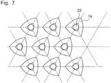
Fig. 7 is a plan view of a substrate surface when a second mask for the second etching step is formed in a method for manufacturing a nitride semiconductor light emitting device according to the embodiment. - Embodiments of the present invention will be described below with reference to the accompanying drawings. The light emitting device described below is presented for the purpose of embodying and exemplifying the technical idea of the present invention, but the present invention is not limited to the following. It is intended that the scope of the invention is not limited to the size, material, shape, relative arrangement, and so on of constitutional components described below unless otherwise specified, and are merely explanatory examples. The size, positional relation, and so on of members illustrated by the respective drawings may be sometimes exaggerated for clear explanation. Furthermore, the respective elements constituting the present invention may include an aspect in which a plurality of elements are constituted from the identical member and one member is allowed to serve as a plurality of elements. To the contrary, a plurality of member can also share the function of one member.
- As shown in
Fig. 1 , the nitride semiconductor light emitting device according to an embodiment of the present invention is provided with a semiconductor laminated structure 2 in which abase layer 21, a first conductive layer (n-type layer) 22, an active layer (emissive layer) 23 and a second conductive layer (p-type layer) 24 are sequentially laminated on asapphire substrate 10, and a plurality of projections (dimples) 1, each having a generally pyramidal shape with a substantially sharpened tip, are provided on a surface of thesubstrate 10 on which thebase layer 21 is grown. - In the nitride semiconductor light emitting device of the embodiment constituted as mentioned above, as described in detail hereinafter, because the
base layer 21, the first conductive layer (n-type layer) 22, the active layer (emissive layer) 23 and the second conductive layer (p-type layer) 24, each being made of a nitride semiconductor, are grown on a surface of thesubstrate 10 provided with a plurality of projections (dimple) 1, each having a generally pyramidal shape with a substantially sharpened tip, the semiconductor layers can be grown with satisfactory crystallinity. - In the semiconductor light emitting device of the embodiment, it also becomes possible to efficiently reflect light emitted from the emissive layer 23 in the light emission direction by a plurality of
projections 1, each having a generally pyramidal shape with a substantially sharpened tip, and thus light extraction efficiency can be enhanced. - Specifically, light that propagates in the transverse direction can be reflected and diffracted on
projection 1, particularly an inclined surface ofprojection 1. - In the embodiment, the projection (dimple) 1 is formed into a generally triangular pyramid shape, as shown in
Figs. 2(a) and 2(b) , - (i) a bottom surface of the projection has a generally triangle shape (generally triangle shape in which the
respective sides - (ii) three
inclined surfaces projection 1 respectively have an outwardly bulged generally triangle shape and also respectively include inclination change lines (etching change lines) L11, L12 and L13 in the middle thereof, and inclination discontinuously varies at the inclination change line as the border. - More specifically, in the respective
inclined surfaces inclined surfaces - The projection (dimple) 1 has a generally triangular pyramid shape and a vertex t1 thereof is substantially sharpened.
- As used herein, a substantially sharpened vertex means that a vertex portion (top surface) of the
projection 1 becomes smaller so that a nitride semiconductor does not grow from the vertex of the projection (dimple) 1. - In the semiconductor light emitting device of the embodiment constituted as mentioned above, light that propagates in a surface direction of a substrate among light emitted from an emissive layer 23 is irregularly reflected or diffracted by a surface between
projections 1 of a substrate surface andinclined surfaces projection 1. - Particularly, as shown in
Figs. 2(a) and 2(b) , becauseinclined surfaces projection 1 of the present embodiment are outwardly bulged curved surfaces, light incident like a so-called convex mirror is diffused and reflected so as to be spread. Furthermore, because inclination discontinuously varies atinclination change lines - The
projections 1 having a generally triangular pyramid shape of the present embodiment being discussed can be formed by setting the crystal form of a substrate, the plane direction of a substrate surface on whichprojection 1 are formed, the mask shape and size, and the etching conditions according to the objective shape. - For example, when a circular first mask is formed on a surface made of the C-plane of a sapphire substrate and etching is carried out, the portion on which no mask is formed is removed by etching to form a circular projection reflecting a mask shape faithfully in an initial stage. As etching proceeds, an influence of direction dependency of an etching rate (an etching proceeding rate varies depending on a direction) caused by a crystal form is exerted, resulting in a shape reflecting the crystal form.
- Specifically, because the etching rate varies depending on an etching progress direction, etching proceeds as a result of reflecting of the crystal form, and thus three vertices of a bottom portion and a ridge line of a triangular pyramid gradually become clear to form a
lower projection 1a having a generally triangular pyramid-shape below a circular mask. A top surface of thelower projection 1a having a generally triangular pyramid-shape is etched in a generally triangular shape and the area becomes smaller than that of the circular mask by undercut. A bottom surface and a top surface of thelower projection 1a becomes a generally triangle shape in which the respective sides are outwardly bulged in a circular arc shape. As etching proceeds, the area becomes smaller and also a curvature radius of a circular arc of each side becomes larger, and thus each side becomes linear. - In the present embodiment being discussed, after the
lower projection 1a is formed and a first mask is removed, a second mask is formed on a top surface of thelower projection 1a or etching is carried out without forming the second mask, thereby further forming anupper projection 1b having a triangular pyramid shape on thelower projection 1a to form a projection (dimple) 1 having a generally triangular pyramid shape, includinginclined surfaces - In the present embodiment being discussed, in case the lower projection is formed by etching and the upper projection is formed by etching, when an etching time is prolonged, it is possible to form a
projection 1 into a generally triangular pyramid shape in which therespective sides inclined surfaces projection 1 into a generally triangular pyramid shape in which therespective sides surfaces - Also,
projections 1 on the substrate enable an improvement in optical output and light extraction efficiency and, in case thebase layer 21 is grown,inclined surfaces projection 1 serve as a surface of suppressing the growth of the base layer 21 (also referred to as a crystal growth-suppression surface) and enables promotion of the growth of a base layer grown from a surface between projections 1 (hereinafter referred to as a crystal growth surface) in a transverse direction to form thebase layer 21 having a surface with less crystal defects. Accordingly, it is preferred that projections constituting the crystal growth-suppression surface are uniformly distributed in the crystal growth surface, and are regularly arranged in a mutually separated state as shown inFigs. 3 to 4 . -
Fig. 3 is a triangular lattice point arrangement, andFig. 4 is a square lattice point arrangement. - In a nitride semiconductor grown from the crystal growth surface in a lengthwise direction, because dislocations caused by a difference between a lattice constant of a substrate and a lattice constant of a nitride semiconductor tend to extend in a growth direction and to appear on a surface,
projections 1 on the substrate are preferably formed at a high density. In this manner, whenprojections 1 are arranged at a high density, a ratio of an area of the crystal growth-suppression surface to the crystal growth surface becomes higher. Therefore, a ratio of a nitride semiconductor grown in the transverse direction, which covers the crystal growth-suppression surface, increases and thus dislocations extending in the growth direction are confined within thebase layer 21 and dislocations or "pits" that appear on the surface can be decreased. - Furthermore, regarding
projections 1 of the present embodiment, because the inclination at the side above inclination change lines L11, L12 and L13 (vertex side) is more gentle than that at the side below inclination change lines (bottom surface side) in the respectiveinclined surfaces - Additional examples of the regular and high-density arrangement of the
projection 1 include, in addition to the triangular lattice point arrangement and the square lattice point arrangement as shown inFigs. 3 to 4 , arrangements such as a parallelogram lattice point arrangement and a rectangular lattice point arrangement. - This regular structure may be arranged with the same regularity in the entire substrate surface, or may be arranged with the different regularity according to electrode arrangement of a semiconductor device structure formed on a substrate.
- In this manner, in order to grow a nitride semiconductor having satisfactory crystallinity, the height of the
projection 1 is set within a range of 0.5 µm or more and 2 µm or less, and preferably within a range of 0.7 µm or more and 1.2 µm or less, and the interval (interval of the narrowest portion) ofprojections 1 is set within a range of 0.5 µm or more and 2 µm or less, and preferably 1.5 µm or less. - One side (a linear distance between vertices of a bottom surface) of the bottom surface of the
projection 1 is set within a range of 0.5 µm or more and 3 µm or less, and preferably within a range of 0.7 µm or more and 2 µm or less. - It is possible to form a
projection 1, that includes a substantially sharpened vertex t1 and also includesinclined surfaces substrate 10, for example, by a two-stage etching described below. - In the present production method, first, as shown in
Fig. 5 , a circularfirst mask 19 is formed on the C-plane (0001) of asapphire substrate 10 and, after etching a substrate, thefirst mask 19 is removed. - Whereby, a generally triangular pyramid-shaped
lower projection 1a including a generally triangular top surface is formed (Fig. 6 ). - The etching method includes a wet etching method and a dry etching method, and any etching method may be used in the present invention. Specifically, a vapor phase etching method, a plasma etching method and a reactive ion etching method can be used as the dry etching method. Examples of an etching gas used in the case of etching include C1-based and F-based gases, for example, Cl2, SiCl4, BCl3, HBr, SF6, CHF3, C4F8, CF4, and an inert gas such as Ar.
- It is possible to use, as an etching solution for wet etching, phosphoric acid, or pyrophosphoric acid, or mixed acid prepared by adding sulfuric acid thereto, or potassium hydroxide in case of a sapphire substrate of Example. At this time, silicon oxide such as SiO2 can be appropriately selected as a mask material according to a substrate material and an etching solution therefor, and examples thereof include oxides of at least one element selected from the group consisting of V, Zr, Nb, Hf, Ti, Ta and Al, and nitrides of at least one element selected from the group consisting of Si, B and Al.
- Next, as shown in
Fig. 7 , after removing thefirst mask 19, a circularsecond mask 20 is formed on a top surface of thelower projection 1a, or thesubstrate 1 is further etched without forming thesecond mask 20. - In this etching step, etching is allowed to proceed until at least an upper projection having a substantially sharpened tip is formed on the top surface of the lower projection.
- This etching method may be either a wet etching method or a dry etching method similar to the first etching step.
- It is also possible to employ, as the etching method, an etching method that is different from that of the first etching step. That is, the wet etching method may be used in the first etching step and the drying etching method may be used in the second etching step, or the method may be alternated.
- In the first etching step and the second etching step, the etching gas or etching solution may vary.
- It is possible to form a
projection 1, that includes a substantially sharpened vertex t1 and also includesinclined surfaces substrate 10, for example, by the aforementioned two-stage etching described. - As mentioned above, when a nitride semiconductor is grown on the C-plane (0001) of sapphire, on which a plurality of tip-sharpened
projections 1 includinginclined surfaces inclined surfaces projection 1 is suppressed (the nitride semiconductor is not substantially grown). - Whereby, the nitride semiconductor grown from the C-plane (0001) surface of sapphire between
projections 1 grows on the inclined surface of theprojection 1 in the transverse direction, and covers theprojection 1 as the growth to obtain a flat GaN surface with less crystal defects, and thus it becomes possible to form, on the flat GaN surface with less crystal defects, a light emitting device structure in which a nitride semiconductor layer with less crystal defects has been laminated. - As shown in
Fig. 1 , a light emitting device structure includes, on a substrate, a laminated structure 2 including first and second conductive layers 22, 24 and an active layer 23 formed therebetween, and also includes a first electrode and a second electrode formed on the first conductive layer 22 and the second conductive layer 24 exposed by removing a portion of the active layer 23 and the second conductive layer 24. The second electrode includes a translucent ohmic electrode formed over nearly the entire surface of the second conductive layer 24, a pad formed on the translucent ohmic electrode, and a diffusion electrode. - In the formation of a light emitting device, it is possible to use, as a semiconductor grown on a substrate, a gallium nitride-based compound semiconductor material represented by the general formula: InxAlyGa1-x-yN (0 ≤ x ≤ 1, 0 ≤ y ≤ 1, 0 ≤ x + y ≤ 1). As mentioned hereinafter, binary and tertiary mixed crystals thereof can be used particularly suitably. It is possible to apply to, in addition to a nitride semiconductor, other semiconductors such as GaAs- and GaP-based compound semiconductors, AlGaAs- and InAlGaP-based compound semiconductors.
- Examples according to the present invention will be described below.
- On the C-plane (0001) of a sapphire substrate, a SiO2 film was formed, followed by patterning to periodically form a circular
first mask 19 having a diameter of about 1.5 µm. - Subsequently, the substrate was immersed in an etching bath using a mixed acid of phosphoric acid and sulfuric acid as an etching solution and etched at a solution temperature of about 290°C for about 5 minutes until the depth (projection height) becomes about 1 µm.
- Whereby, a
lower projection 1a was formed. - Next, after removing the
first mask 19, the substrate was immersed in an etching bath using a mixed acid of phosphoric acid and sulfuric acid as an etching solution, in a state of absence of a mask, and etched at a solution temperature of about 290°C for about 1 minute until a tip of projection is substantially sharpened to form anupper projection 1b. - A
projection 1 having a height of about 1 µm and a two-stage taper angle was formed by the aforementioned steps. - Subsequently, the substrate was transferred to a MOCVD device, where a 20 nm thick GaN buffer layer grown at a low temperature (about 510°C) was formed on a substrate surface with
projection 1 formed thereon, and GaN was c-axis grown thereon at a high temperature (about 1,050°C) to form abase layer 21 having a flat surface. - On the thus obtained substrate with the
base layer 21 formed thereon, as shown inFig. 1 , an n-type layer 22 such as an n-type contact layer, an active layer 23 and a p-type layer 24 were formed to manufacture a semiconductor device structure. - Specifically, as the first conductive layer 22 (n-type layer), an n-side contact layer having a film thickness of 5 µm made of Si (4.5 × 10¹⁸/cm3) doped GaN, 0.3 µm thick undoped GaN layer, 0.03 µm thick Si (4.5 × 10¹⁸/cm3) doped GaN layers, 5 nm thick undoped GaN layer, a multi-layered film obtained by repeatedly and alternately laminating each 10 layers of 4 nm thick undoped GaN layers and 2 nm thick undoped In0.1Ga0.9N layers are formed on the
aforementioned base layer 21. As the active layer 23, a multiple quantum well structure obtained by repeatedly and alternately laminating each 6 layers of barrier layers having a film thickness of 25 nm made of undoped GaN and well layers having a film thickness of 3 nm made of In0.3Ga0.7Nnd finally laminating a barrier layer is formed on the n-type layer. As the second conductive layer (p-type layer) 24, a p-side multi-layered film layer which has a structure obtained by repeatedly and alternately laminating each 5 layers of 4 nm thick Mg (5 × 10¹⁹/cm3) doped Al0.15Ga0.85N layers and 2.5 nm thick Mg (5 × 10¹⁹/cm3) doped In0.03Ga0.97N layers; and finally laminating with the AlGaN layer formed thereon and a p-side contact layer having a film thickness 0.12 µm made of Mg (1 × 10²⁰/cm3) doped GaN are formed on the active layer. With this, a structure (emission wavelength of 465 nm, blue LED) can be obtained. - The semiconductor device structure was provided with an electrode having a structure in which ITO (about 170 nm) is formed as a translucent ohmic electrode on a surface of a p-type layer 24, that would serve as a surface of an emitting structure portion, and then Rh (about 100 nm), Pt (about 200 nm) and Au (about 500 nm) are laminated in this order on ITO and the n-side contact layer.
-
- 1:
- Projection
- 1a:
- Lower projection
- 1b:
- Upper projection
- 2:
- Semiconductor laminated structure
- 10:
- Substrate
- t1:
- Vertex
- L11, L12 and L13:
- Inclination change lines
- 11k, 12k and 13k:
- Inclined surfaces
- 19:
- First mask
- 20:
- Second mask
- 21:
- Base layer
- 22:
- n-type layer (First conductive layer)
- 23:
- Active layer
- 24:
- p-type layer (Second conductive layer)
-
Embodiment 1. A sapphire substrate having a principal surface on which a nitride semiconductor is grown to form a nitride semiconductor light emitting device, comprising a plurality of projections on the principal surface,
wherein each of the projections has a generally pyramidal shape with a substantially sharpened tip and an inclined surface, the inclined surface being composed of a crystal growth-suppression surface that lessens the growth of the nitride semiconductor in comparison with a substrate surface located between adjacent projections, the inclined surface having an inclination change line at which an inclination angle discontinuously varies. - Embodiment 2. The sapphire substrate according to the features of
embodiment 1, wherein a bottom surface of the projection has a generally polygonal shape with outwardly bulged circular arc-shaped three or more sides, the inclined surface is composed of a plurality of generally triangular inclined surfaces each including both ends of each side and the substantially sharpened tip as a vertex, and an inclination angle of each inclined surface discontinuously varies in the inclination change line. - Embodiment 3. The sapphire substrate according to the features of
embodiment 1 or 2, wherein an inclination angle of the inclined surface above the inclination change line is smaller than that of the inclined surface below the inclination change line. - Embodiment 4. The sapphire substrate as in one of
embodiments 1 to 3, wherein the projections are located separately on the principal surface. - Embodiment 5. The sapphire substrate as in one of
embodiments 1 to 4, wherein the projections are periodically arranged on the principal surface. - Embodiment 6. The sapphire substrate according to the features of embodiment 5, wherein the projections are located on vertexes of a triangular lattice, a quadrangular lattice or a hexagonal lattice.
- Embodiment 7. A nitride semiconductor light emitting device comprising: the sapphire substrate as in one of
embodiments 1 to 6; and a nitride semiconductor layer formed by growing a nitride semiconductor on the principal surface of the sapphire. - Embodiment 8. A method for manufacturing a sapphire substrate for a nitride semiconductor light emitting device, the method comprising:
- a first etching step of forming a first mask on the C-plane of a sapphire substrate, and etching the sapphire substrate using the first mask as an etching mask to form a lower projection having a truncated pyramidal shape,
- a first mask removing step of removing the first mask thereby exposing a top surface of the lower projection, and
- a second etching step of further etching the lower projection whose top surface has been exposed to form an upper projection having a pyramidal shape with a substantially sharpened tip on the lower projection.
- Embodiment 9. The method for manufacturing a sapphire substrate for a nitride semiconductor light emitting device according to the features of embodiment 8, further comprising a second mask forming step of forming second mask on upper surfaces of the lower projection between the first mask removing step and the second etching step.
Claims (7)
- A sapphire substrate having a principal surface of C-plane, comprising a plurality of projections on the principal surface,
wherein each of the projections has a pyramidal shape with a substantially sharpened tip and an inclined surface, the inclined surface being inclined from the C-plane,
characterized by the inclined surface having an inclination change line at which an inclination angle discontinuously varies. - The sapphire substrate according to claim 1, wherein a bottom surface of the projection has a generally polygonal shape with outwardly bulged circular arc-shaped three or more sides, the inclined surface is composed of a plurality of generally triangular inclined surfaces each including both ends of each side and the substantially sharpened tip as a vertex, and an inclination angle of each inclined surface discontinuously varies in the inclination change line.
- The sapphire substrate according to claim 1 or 2, wherein an inclination angle of the inclined surface above the inclination change line is smaller than that of the inclined surface below the inclination change line.
- The sapphire substrate as in one of claims 1 to 3, wherein the projections are located separately on the principal surface.
- The sapphire substrate as in one of claims 1 to 4, wherein the projections are periodically arranged on the principal surface.
- The sapphire substrate according to claim 5, wherein the projections are located on vertexes of a triangular lattice, a quadrangular lattice or a hexagonal lattice.
- A nitride semiconductor light emitting device comprising: the sapphire substrate as in one of claims 1 to 6; and a nitride semiconductor layer formed by growing a nitride semiconductor on the principal surface of the sapphire.
Applications Claiming Priority (3)
| Application Number | Priority Date | Filing Date | Title |
|---|---|---|---|
| JP2010146540 | 2010-06-28 | ||
| PCT/JP2011/064355 WO2012002240A1 (en) | 2010-06-28 | 2011-06-23 | Sapphire substrate, method for producing same, and nitride semiconductor light emitting element |
| EP11800705.3A EP2587556B1 (en) | 2010-06-28 | 2011-06-23 | Method for manufacturing a sapphire substrate and growing a nitride semiconductor light emitting device |
Related Parent Applications (2)
| Application Number | Title | Priority Date | Filing Date |
|---|---|---|---|
| EP11800705.3A Division EP2587556B1 (en) | 2010-06-28 | 2011-06-23 | Method for manufacturing a sapphire substrate and growing a nitride semiconductor light emitting device |
| EP11800705.3A Division-Into EP2587556B1 (en) | 2010-06-28 | 2011-06-23 | Method for manufacturing a sapphire substrate and growing a nitride semiconductor light emitting device |
Publications (2)
| Publication Number | Publication Date |
|---|---|
| EP3352229A1 true EP3352229A1 (en) | 2018-07-25 |
| EP3352229B1 EP3352229B1 (en) | 2024-12-11 |
Family
ID=45351700
Family Applications (2)
| Application Number | Title | Priority Date | Filing Date |
|---|---|---|---|
| EP18153527.9A Active EP3352229B1 (en) | 2010-06-28 | 2011-06-23 | Sapphire substrate and nitride semiconductor light emitting device |
| EP11800705.3A Active EP2587556B1 (en) | 2010-06-28 | 2011-06-23 | Method for manufacturing a sapphire substrate and growing a nitride semiconductor light emitting device |
Family Applications After (1)
| Application Number | Title | Priority Date | Filing Date |
|---|---|---|---|
| EP11800705.3A Active EP2587556B1 (en) | 2010-06-28 | 2011-06-23 | Method for manufacturing a sapphire substrate and growing a nitride semiconductor light emitting device |
Country Status (5)
| Country | Link |
|---|---|
| US (1) | US8779463B2 (en) |
| EP (2) | EP3352229B1 (en) |
| JP (1) | JP5725023B2 (en) |
| TW (1) | TWI608632B (en) |
| WO (1) | WO2012002240A1 (en) |
Families Citing this family (24)
| Publication number | Priority date | Publication date | Assignee | Title |
|---|---|---|---|---|
| JPH0752060A (en) * | 1993-08-13 | 1995-02-28 | Matsushita Electric Works Ltd | Impact wrench |
| EP2624283B1 (en) * | 2010-08-06 | 2021-07-07 | Nichia Corporation | Sapphire substrate and semiconductor light-emitting element |
| JP2012124257A (en) | 2010-12-07 | 2012-06-28 | Toshiba Corp | Semiconductor light-emitting element and method of manufacturing the same |
| TWI429030B (en) * | 2011-05-16 | 2014-03-01 | Sino American Silicon Prod Inc | Light-emitting diode substrate and light-emitting diode |
| KR20130035658A (en) * | 2011-09-30 | 2013-04-09 | 서울옵토디바이스주식회사 | Method for fabricating a substrate for light emitting diode device |
| CN103199165A (en) * | 2012-01-05 | 2013-07-10 | 昆山中辰矽晶有限公司 | Light-emitting diode substrate, processing method thereof and light-emitting diode |
| JP6024533B2 (en) | 2012-03-28 | 2016-11-16 | 日亜化学工業株式会社 | Sapphire substrate, manufacturing method thereof, and nitride semiconductor light emitting device |
| CN104813489B (en) | 2012-11-23 | 2018-01-02 | 首尔伟傲世有限公司 | Light emitting diode and its manufacture method |
| CN103325906B (en) * | 2013-06-04 | 2016-04-27 | 江苏新广联科技股份有限公司 | Graph substrate of adjustable LED lighting angle and preparation method thereof |
| CN105283969B (en) | 2013-06-19 | 2019-12-17 | 亮锐控股有限公司 | LEDs with patterned surface features based on emission field patterns |
| CN104638068B (en) * | 2013-11-07 | 2018-08-24 | 上海蓝光科技有限公司 | A kind of substrat structure and preparation method thereof being used for the growth of III-V group-III nitride |
| JP6183189B2 (en) * | 2013-12-02 | 2017-08-23 | 日亜化学工業株式会社 | Method for manufacturing light emitting device |
| CN103871844B (en) * | 2014-03-31 | 2017-04-05 | 海迪科(南通)光电科技有限公司 | Bottom for improving graphical sapphire substrate etches abnormal method |
| JP6248786B2 (en) * | 2014-04-25 | 2017-12-20 | 日亜化学工業株式会社 | Nitride semiconductor device and manufacturing method thereof |
| JP6550926B2 (en) | 2014-05-30 | 2019-07-31 | 日亜化学工業株式会社 | Nitride semiconductor device and manufacturing method thereof |
| JP6375890B2 (en) * | 2014-11-18 | 2018-08-22 | 日亜化学工業株式会社 | Nitride semiconductor device and manufacturing method thereof |
| JP6135751B2 (en) * | 2015-02-18 | 2017-05-31 | 日亜化学工業株式会社 | Light emitting element |
| US9773946B2 (en) | 2015-02-18 | 2017-09-26 | Nichia Corporation | Light-emitting element comprising a partitioned sapphire substrate |
| WO2017099086A1 (en) * | 2015-12-10 | 2017-06-15 | 王子ホールディングス株式会社 | Substrate, optical element, mold, organic light-emitting element, organic thin-film solar cell, and method for producing substrate |
| JP6443524B2 (en) * | 2017-11-22 | 2018-12-26 | 日亜化学工業株式会社 | Nitride semiconductor device and manufacturing method thereof |
| JP7305428B2 (en) * | 2018-06-05 | 2023-07-10 | 株式会社小糸製作所 | Semiconductor growth substrate, semiconductor device, semiconductor light-emitting device, and semiconductor device manufacturing method |
| JP7238897B2 (en) * | 2018-09-14 | 2023-03-14 | 王子ホールディングス株式会社 | PROJECTED STRUCTURE, SUBSTRATE FOR LIGHT EMITTING DEVICE, MANUFACTURING METHOD THEREOF, AND LIGHT EMITTING DEVICE |
| CN114023851B (en) * | 2021-09-09 | 2023-10-13 | 华灿光电(浙江)有限公司 | Epitaxial wafer of deep ultraviolet light-emitting diode and preparation method thereof |
| US20250179626A1 (en) * | 2022-03-04 | 2025-06-05 | Soulbrain Co., Ltd. | Thin film modification composition, method of forming thin film using thin film modification composition, semiconductor substrate including thin film, and semiconductor device including semiconductor substrate |
Citations (2)
| Publication number | Priority date | Publication date | Assignee | Title |
|---|---|---|---|---|
| EP1667241A1 (en) * | 2003-08-19 | 2006-06-07 | Nichia Corporation | Semiconductor device |
| JP2008177528A (en) | 2006-12-21 | 2008-07-31 | Nichia Chem Ind Ltd | Manufacturing method of substrate for semiconductor light emitting device and semiconductor light emitting device using the same |
Family Cites Families (1)
| Publication number | Priority date | Publication date | Assignee | Title |
|---|---|---|---|---|
| TWI413279B (en) * | 2008-06-20 | 2013-10-21 | 豐田合成股份有限公司 | Group III nitride semiconductor light-emitting device, method of manufacturing the same, and lamp |
-
2011
- 2011-06-23 JP JP2012522581A patent/JP5725023B2/en active Active
- 2011-06-23 EP EP18153527.9A patent/EP3352229B1/en active Active
- 2011-06-23 EP EP11800705.3A patent/EP2587556B1/en active Active
- 2011-06-23 WO PCT/JP2011/064355 patent/WO2012002240A1/en not_active Ceased
- 2011-06-24 US US13/168,604 patent/US8779463B2/en active Active
- 2011-06-28 TW TW100122713A patent/TWI608632B/en active
Patent Citations (3)
| Publication number | Priority date | Publication date | Assignee | Title |
|---|---|---|---|---|
| EP1667241A1 (en) * | 2003-08-19 | 2006-06-07 | Nichia Corporation | Semiconductor device |
| JP2008177528A (en) | 2006-12-21 | 2008-07-31 | Nichia Chem Ind Ltd | Manufacturing method of substrate for semiconductor light emitting device and semiconductor light emitting device using the same |
| US20080303042A1 (en) * | 2006-12-21 | 2008-12-11 | Nichia Corporation | Method for manufacturing substrate for semiconductor light emitting element and semiconductor light emitting element using the same |
Non-Patent Citations (1)
| Title |
|---|
| CHEN Y-J ET AL: "Fabrication of High-Power InGaN-Based Light-Emitting Diode Chips on Pyramidally Patterned Sapphire Substrate", JAPANESE JOURNAL OF APPLIED PHYSICS, JAPAN SOCIETY OF APPLIED PHYSICS, JP, vol. 49, no. 2, 1 February 2010 (2010-02-01), pages 20201 - 1, XP001554123, ISSN: 0021-4922, [retrieved on 20100205], DOI: 10.1143/JJAP.49.020201 * |
Also Published As
| Publication number | Publication date |
|---|---|
| EP3352229B1 (en) | 2024-12-11 |
| TW201214766A (en) | 2012-04-01 |
| US20110316041A1 (en) | 2011-12-29 |
| US8779463B2 (en) | 2014-07-15 |
| WO2012002240A1 (en) | 2012-01-05 |
| EP2587556B1 (en) | 2018-05-02 |
| EP2587556A4 (en) | 2014-06-11 |
| TWI608632B (en) | 2017-12-11 |
| JPWO2012002240A1 (en) | 2013-08-22 |
| JP5725023B2 (en) | 2015-05-27 |
| EP2587556A1 (en) | 2013-05-01 |
Similar Documents
| Publication | Publication Date | Title |
|---|---|---|
| EP3352229B1 (en) | Sapphire substrate and nitride semiconductor light emitting device | |
| EP2644756B1 (en) | Patterned sapphire substrate and method for manufacturing the same and nitride semiconductor light emitting element using that sapphire substrate | |
| EP1596443B1 (en) | Light-emitting element | |
| JP5641025B2 (en) | Manufacturing method of substrate for semiconductor light emitting device and semiconductor light emitting device using the same | |
| KR101417541B1 (en) | Semiconductor light emitting element | |
| JP4063259B2 (en) | Semiconductor device and manufacturing method thereof | |
| US7906791B2 (en) | Semiconductor light emitting element | |
| CN104813489B (en) | Light emitting diode and its manufacture method | |
| JP5673581B2 (en) | Group III nitride semiconductor light emitting device manufacturing method, group III nitride semiconductor light emitting device, lamp, and reticle | |
| EP1378949A1 (en) | Semiconductor light-emitting device | |
| JP5707978B2 (en) | Semiconductor light emitting device substrate, method of manufacturing the same, and semiconductor light emitting device using the substrate | |
| JP2012114407A (en) | Method for fabricating vertical light emitting devices and substrate module for the same | |
| US8889450B2 (en) | Light emitting diode and method for fabricating the same | |
| JP2003273470A (en) | III-nitride semiconductor laser device | |
| JP2011238884A (en) | Substrate for epitaxial growth, growth method of gan-based semiconductor crystal, semiconductor structure, and gan-based led element | |
| CN116583954A (en) | Substrate structure and preparation method thereof, light-emitting device and preparation method thereof | |
| KR20120010351A (en) | Manufacturing method of semiconductor light emitting device | |
| KR20100021243A (en) | Light emitting device and method of manufacturing the same | |
| TW202427820A (en) | Light-emitting device |
Legal Events
| Date | Code | Title | Description |
|---|---|---|---|
| PUAI | Public reference made under article 153(3) epc to a published international application that has entered the european phase |
Free format text: ORIGINAL CODE: 0009012 |
|
| STAA | Information on the status of an ep patent application or granted ep patent |
Free format text: STATUS: THE APPLICATION HAS BEEN PUBLISHED |
|
| AC | Divisional application: reference to earlier application |
Ref document number: 2587556 Country of ref document: EP Kind code of ref document: P |
|
| AK | Designated contracting states |
Kind code of ref document: A1 Designated state(s): AL AT BE BG CH CY CZ DE DK EE ES FI FR GB GR HR HU IE IS IT LI LT LU LV MC MK MT NL NO PL PT RO RS SE SI SK SM TR |
|
| STAA | Information on the status of an ep patent application or granted ep patent |
Free format text: STATUS: REQUEST FOR EXAMINATION WAS MADE |
|
| 17P | Request for examination filed |
Effective date: 20190125 |
|
| RBV | Designated contracting states (corrected) |
Designated state(s): AL AT BE BG CH CY CZ DE DK EE ES FI FR GB GR HR HU IE IS IT LI LT LU LV MC MK MT NL NO PL PT RO RS SE SI SK SM TR |
|
| STAA | Information on the status of an ep patent application or granted ep patent |
Free format text: STATUS: EXAMINATION IS IN PROGRESS |
|
| 17Q | First examination report despatched |
Effective date: 20210921 |
|
| P01 | Opt-out of the competence of the unified patent court (upc) registered |
Effective date: 20230522 |
|
| REG | Reference to a national code |
Ref country code: DE Ref legal event code: R079 Free format text: PREVIOUS MAIN CLASS: H01L0033320000 Ipc: H01L0033120000 Ref country code: DE Ref legal event code: R079 Ref document number: 602011075152 Country of ref document: DE Free format text: PREVIOUS MAIN CLASS: H01L0033320000 Ipc: H01L0033120000 |
|
| RIC1 | Information provided on ipc code assigned before grant |
Ipc: C30B 25/18 20060101ALI20230630BHEP Ipc: C30B 29/60 20060101ALI20230630BHEP Ipc: C30B 29/40 20060101ALI20230630BHEP Ipc: H01L 33/20 20100101ALI20230630BHEP Ipc: H01L 33/32 20100101ALI20230630BHEP Ipc: H01L 33/12 20100101AFI20230630BHEP |
|
| GRAP | Despatch of communication of intention to grant a patent |
Free format text: ORIGINAL CODE: EPIDOSNIGR1 |
|
| STAA | Information on the status of an ep patent application or granted ep patent |
Free format text: STATUS: GRANT OF PATENT IS INTENDED |
|
| RAP3 | Party data changed (applicant data changed or rights of an application transferred) |
Owner name: NICHIA CORPORATION |
|
| INTG | Intention to grant announced |
Effective date: 20240724 |
|
| GRAS | Grant fee paid |
Free format text: ORIGINAL CODE: EPIDOSNIGR3 |
|
| GRAA | (expected) grant |
Free format text: ORIGINAL CODE: 0009210 |
|
| STAA | Information on the status of an ep patent application or granted ep patent |
Free format text: STATUS: THE PATENT HAS BEEN GRANTED |
|
| REG | Reference to a national code |
Ref country code: DE Ref legal event code: R079 Ref document number: 602011075152 Country of ref document: DE Free format text: PREVIOUS MAIN CLASS: H01L0033120000 Ipc: H10H0020815000 |
|
| AC | Divisional application: reference to earlier application |
Ref document number: 2587556 Country of ref document: EP Kind code of ref document: P |
|
| AK | Designated contracting states |
Kind code of ref document: B1 Designated state(s): AL AT BE BG CH CY CZ DE DK EE ES FI FR GB GR HR HU IE IS IT LI LT LU LV MC MK MT NL NO PL PT RO RS SE SI SK SM TR |
|
| REG | Reference to a national code |
Ref country code: GB Ref legal event code: FG4D |
|
| REG | Reference to a national code |
Ref country code: CH Ref legal event code: EP |
|
| REG | Reference to a national code |
Ref country code: DE Ref legal event code: R096 Ref document number: 602011075152 Country of ref document: DE |
|
| REG | Reference to a national code |
Ref country code: IE Ref legal event code: FG4D |
|
| REG | Reference to a national code |
Ref country code: LT Ref legal event code: MG9D |
|
| PG25 | Lapsed in a contracting state [announced via postgrant information from national office to epo] |
Ref country code: HR Free format text: LAPSE BECAUSE OF FAILURE TO SUBMIT A TRANSLATION OF THE DESCRIPTION OR TO PAY THE FEE WITHIN THE PRESCRIBED TIME-LIMIT Effective date: 20241211 |
|
| PG25 | Lapsed in a contracting state [announced via postgrant information from national office to epo] |
Ref country code: FI Free format text: LAPSE BECAUSE OF FAILURE TO SUBMIT A TRANSLATION OF THE DESCRIPTION OR TO PAY THE FEE WITHIN THE PRESCRIBED TIME-LIMIT Effective date: 20241211 |
|
| PG25 | Lapsed in a contracting state [announced via postgrant information from national office to epo] |
Ref country code: BG Free format text: LAPSE BECAUSE OF FAILURE TO SUBMIT A TRANSLATION OF THE DESCRIPTION OR TO PAY THE FEE WITHIN THE PRESCRIBED TIME-LIMIT Effective date: 20241211 |
|
| REG | Reference to a national code |
Ref country code: NL Ref legal event code: MP Effective date: 20241211 |
|
| PG25 | Lapsed in a contracting state [announced via postgrant information from national office to epo] |
Ref country code: ES Free format text: LAPSE BECAUSE OF FAILURE TO SUBMIT A TRANSLATION OF THE DESCRIPTION OR TO PAY THE FEE WITHIN THE PRESCRIBED TIME-LIMIT Effective date: 20241211 |
|
| PG25 | Lapsed in a contracting state [announced via postgrant information from national office to epo] |
Ref country code: NO Free format text: LAPSE BECAUSE OF FAILURE TO SUBMIT A TRANSLATION OF THE DESCRIPTION OR TO PAY THE FEE WITHIN THE PRESCRIBED TIME-LIMIT Effective date: 20250311 |
|
| PG25 | Lapsed in a contracting state [announced via postgrant information from national office to epo] |
Ref country code: LV Free format text: LAPSE BECAUSE OF FAILURE TO SUBMIT A TRANSLATION OF THE DESCRIPTION OR TO PAY THE FEE WITHIN THE PRESCRIBED TIME-LIMIT Effective date: 20241211 Ref country code: GR Free format text: LAPSE BECAUSE OF FAILURE TO SUBMIT A TRANSLATION OF THE DESCRIPTION OR TO PAY THE FEE WITHIN THE PRESCRIBED TIME-LIMIT Effective date: 20250312 |
|
| PG25 | Lapsed in a contracting state [announced via postgrant information from national office to epo] |
Ref country code: RS Free format text: LAPSE BECAUSE OF FAILURE TO SUBMIT A TRANSLATION OF THE DESCRIPTION OR TO PAY THE FEE WITHIN THE PRESCRIBED TIME-LIMIT Effective date: 20250311 |
|
| PG25 | Lapsed in a contracting state [announced via postgrant information from national office to epo] |
Ref country code: NL Free format text: LAPSE BECAUSE OF FAILURE TO SUBMIT A TRANSLATION OF THE DESCRIPTION OR TO PAY THE FEE WITHIN THE PRESCRIBED TIME-LIMIT Effective date: 20241211 |
|
| REG | Reference to a national code |
Ref country code: AT Ref legal event code: MK05 Ref document number: 1751100 Country of ref document: AT Kind code of ref document: T Effective date: 20241211 |
|
| PG25 | Lapsed in a contracting state [announced via postgrant information from national office to epo] |
Ref country code: SM Free format text: LAPSE BECAUSE OF FAILURE TO SUBMIT A TRANSLATION OF THE DESCRIPTION OR TO PAY THE FEE WITHIN THE PRESCRIBED TIME-LIMIT Effective date: 20241211 |
|
| PG25 | Lapsed in a contracting state [announced via postgrant information from national office to epo] |
Ref country code: PL Free format text: LAPSE BECAUSE OF FAILURE TO SUBMIT A TRANSLATION OF THE DESCRIPTION OR TO PAY THE FEE WITHIN THE PRESCRIBED TIME-LIMIT Effective date: 20241211 |
|
| PGFP | Annual fee paid to national office [announced via postgrant information from national office to epo] |
Ref country code: DE Payment date: 20250429 Year of fee payment: 15 |
|
| PG25 | Lapsed in a contracting state [announced via postgrant information from national office to epo] |
Ref country code: IS Free format text: LAPSE BECAUSE OF FAILURE TO SUBMIT A TRANSLATION OF THE DESCRIPTION OR TO PAY THE FEE WITHIN THE PRESCRIBED TIME-LIMIT Effective date: 20250411 |
|
| PG25 | Lapsed in a contracting state [announced via postgrant information from national office to epo] |
Ref country code: PT Free format text: LAPSE BECAUSE OF FAILURE TO SUBMIT A TRANSLATION OF THE DESCRIPTION OR TO PAY THE FEE WITHIN THE PRESCRIBED TIME-LIMIT Effective date: 20250411 |
|
| PG25 | Lapsed in a contracting state [announced via postgrant information from national office to epo] |
Ref country code: EE Free format text: LAPSE BECAUSE OF FAILURE TO SUBMIT A TRANSLATION OF THE DESCRIPTION OR TO PAY THE FEE WITHIN THE PRESCRIBED TIME-LIMIT Effective date: 20241211 |
|
| PG25 | Lapsed in a contracting state [announced via postgrant information from national office to epo] |
Ref country code: RO Free format text: LAPSE BECAUSE OF FAILURE TO SUBMIT A TRANSLATION OF THE DESCRIPTION OR TO PAY THE FEE WITHIN THE PRESCRIBED TIME-LIMIT Effective date: 20241211 Ref country code: AT Free format text: LAPSE BECAUSE OF FAILURE TO SUBMIT A TRANSLATION OF THE DESCRIPTION OR TO PAY THE FEE WITHIN THE PRESCRIBED TIME-LIMIT Effective date: 20241211 |
|
| PG25 | Lapsed in a contracting state [announced via postgrant information from national office to epo] |
Ref country code: SK Free format text: LAPSE BECAUSE OF FAILURE TO SUBMIT A TRANSLATION OF THE DESCRIPTION OR TO PAY THE FEE WITHIN THE PRESCRIBED TIME-LIMIT Effective date: 20241211 |
|
| PG25 | Lapsed in a contracting state [announced via postgrant information from national office to epo] |
Ref country code: CZ Free format text: LAPSE BECAUSE OF FAILURE TO SUBMIT A TRANSLATION OF THE DESCRIPTION OR TO PAY THE FEE WITHIN THE PRESCRIBED TIME-LIMIT Effective date: 20241211 |
|
| PG25 | Lapsed in a contracting state [announced via postgrant information from national office to epo] |
Ref country code: IT Free format text: LAPSE BECAUSE OF FAILURE TO SUBMIT A TRANSLATION OF THE DESCRIPTION OR TO PAY THE FEE WITHIN THE PRESCRIBED TIME-LIMIT Effective date: 20241211 |
|
| PG25 | Lapsed in a contracting state [announced via postgrant information from national office to epo] |
Ref country code: SE Free format text: LAPSE BECAUSE OF FAILURE TO SUBMIT A TRANSLATION OF THE DESCRIPTION OR TO PAY THE FEE WITHIN THE PRESCRIBED TIME-LIMIT Effective date: 20241211 |
|
| REG | Reference to a national code |
Ref country code: DE Ref legal event code: R097 Ref document number: 602011075152 Country of ref document: DE |
|
| PG25 | Lapsed in a contracting state [announced via postgrant information from national office to epo] |
Ref country code: DK Free format text: LAPSE BECAUSE OF FAILURE TO SUBMIT A TRANSLATION OF THE DESCRIPTION OR TO PAY THE FEE WITHIN THE PRESCRIBED TIME-LIMIT Effective date: 20241211 |
|
| PLBE | No opposition filed within time limit |
Free format text: ORIGINAL CODE: 0009261 |
|
| STAA | Information on the status of an ep patent application or granted ep patent |
Free format text: STATUS: NO OPPOSITION FILED WITHIN TIME LIMIT |
|
| REG | Reference to a national code |
Ref country code: CH Ref legal event code: L10 Free format text: ST27 STATUS EVENT CODE: U-0-0-L10-L00 (AS PROVIDED BY THE NATIONAL OFFICE) Effective date: 20251022 |
|
| 26N | No opposition filed |
Effective date: 20250912 |
|
| REG | Reference to a national code |
Ref country code: CH Ref legal event code: H13 Free format text: ST27 STATUS EVENT CODE: U-0-0-H10-H13 (AS PROVIDED BY THE NATIONAL OFFICE) Effective date: 20260127 |
|
| PG25 | Lapsed in a contracting state [announced via postgrant information from national office to epo] |
Ref country code: MC Free format text: LAPSE BECAUSE OF FAILURE TO SUBMIT A TRANSLATION OF THE DESCRIPTION OR TO PAY THE FEE WITHIN THE PRESCRIBED TIME-LIMIT Effective date: 20241211 |
|
| PG25 | Lapsed in a contracting state [announced via postgrant information from national office to epo] |
Ref country code: LU Free format text: LAPSE BECAUSE OF NON-PAYMENT OF DUE FEES Effective date: 20250623 |
|
| GBPC | Gb: european patent ceased through non-payment of renewal fee |
Effective date: 20250623 |
|
| REG | Reference to a national code |
Ref country code: BE Ref legal event code: MM Effective date: 20250630 |
|
| PG25 | Lapsed in a contracting state [announced via postgrant information from national office to epo] |
Ref country code: GB Free format text: LAPSE BECAUSE OF NON-PAYMENT OF DUE FEES Effective date: 20250623 |
|
| PG25 | Lapsed in a contracting state [announced via postgrant information from national office to epo] |
Ref country code: IE Free format text: LAPSE BECAUSE OF NON-PAYMENT OF DUE FEES Effective date: 20250623 |
|
| PG25 | Lapsed in a contracting state [announced via postgrant information from national office to epo] |
Ref country code: BE Free format text: LAPSE BECAUSE OF NON-PAYMENT OF DUE FEES Effective date: 20250630 |
|
| PG25 | Lapsed in a contracting state [announced via postgrant information from national office to epo] |
Ref country code: FR Free format text: LAPSE BECAUSE OF NON-PAYMENT OF DUE FEES Effective date: 20250630 |
|
| PG25 | Lapsed in a contracting state [announced via postgrant information from national office to epo] |
Ref country code: CH Free format text: LAPSE BECAUSE OF NON-PAYMENT OF DUE FEES Effective date: 20250630 |