EP3352219A1 - Solid-state imaging element, electronic device and method for manufacturing solid-state imaging element - Google Patents
Solid-state imaging element, electronic device and method for manufacturing solid-state imaging element Download PDFInfo
- Publication number
- EP3352219A1 EP3352219A1 EP16846293.5A EP16846293A EP3352219A1 EP 3352219 A1 EP3352219 A1 EP 3352219A1 EP 16846293 A EP16846293 A EP 16846293A EP 3352219 A1 EP3352219 A1 EP 3352219A1
- Authority
- EP
- European Patent Office
- Prior art keywords
- region
- film
- solid
- state image
- semiconductor substrate
- Prior art date
- Legal status (The legal status is an assumption and is not a legal conclusion. Google has not performed a legal analysis and makes no representation as to the accuracy of the status listed.)
- Granted
Links
Images




Classifications
-
- H—ELECTRICITY
- H10—SEMICONDUCTOR DEVICES; ELECTRIC SOLID-STATE DEVICES NOT OTHERWISE PROVIDED FOR
- H10F—INORGANIC SEMICONDUCTOR DEVICES SENSITIVE TO INFRARED RADIATION, LIGHT, ELECTROMAGNETIC RADIATION OF SHORTER WAVELENGTH OR CORPUSCULAR RADIATION
- H10F39/00—Integrated devices, or assemblies of multiple devices, comprising at least one element covered by group H10F30/00, e.g. radiation detectors comprising photodiode arrays
- H10F39/80—Constructional details of image sensors
- H10F39/805—Coatings
-
- H—ELECTRICITY
- H04—ELECTRIC COMMUNICATION TECHNIQUE
- H04N—PICTORIAL COMMUNICATION, e.g. TELEVISION
- H04N23/00—Cameras or camera modules comprising electronic image sensors; Control thereof
- H04N23/80—Camera processing pipelines; Components thereof
- H04N23/84—Camera processing pipelines; Components thereof for processing colour signals
-
- H—ELECTRICITY
- H10—SEMICONDUCTOR DEVICES; ELECTRIC SOLID-STATE DEVICES NOT OTHERWISE PROVIDED FOR
- H10F—INORGANIC SEMICONDUCTOR DEVICES SENSITIVE TO INFRARED RADIATION, LIGHT, ELECTROMAGNETIC RADIATION OF SHORTER WAVELENGTH OR CORPUSCULAR RADIATION
- H10F30/00—Individual radiation-sensitive semiconductor devices in which radiation controls the flow of current through the devices, e.g. photodetectors
- H10F30/20—Individual radiation-sensitive semiconductor devices in which radiation controls the flow of current through the devices, e.g. photodetectors the devices having potential barriers, e.g. phototransistors
- H10F30/21—Individual radiation-sensitive semiconductor devices in which radiation controls the flow of current through the devices, e.g. photodetectors the devices having potential barriers, e.g. phototransistors the devices being sensitive to infrared, visible or ultraviolet radiation
- H10F30/22—Individual radiation-sensitive semiconductor devices in which radiation controls the flow of current through the devices, e.g. photodetectors the devices having potential barriers, e.g. phototransistors the devices being sensitive to infrared, visible or ultraviolet radiation the devices having only one potential barrier, e.g. photodiodes
- H10F30/225—Individual radiation-sensitive semiconductor devices in which radiation controls the flow of current through the devices, e.g. photodetectors the devices having potential barriers, e.g. phototransistors the devices being sensitive to infrared, visible or ultraviolet radiation the devices having only one potential barrier, e.g. photodiodes the potential barrier working in avalanche mode, e.g. avalanche photodiodes
-
- H—ELECTRICITY
- H10—SEMICONDUCTOR DEVICES; ELECTRIC SOLID-STATE DEVICES NOT OTHERWISE PROVIDED FOR
- H10F—INORGANIC SEMICONDUCTOR DEVICES SENSITIVE TO INFRARED RADIATION, LIGHT, ELECTROMAGNETIC RADIATION OF SHORTER WAVELENGTH OR CORPUSCULAR RADIATION
- H10F30/00—Individual radiation-sensitive semiconductor devices in which radiation controls the flow of current through the devices, e.g. photodetectors
- H10F30/20—Individual radiation-sensitive semiconductor devices in which radiation controls the flow of current through the devices, e.g. photodetectors the devices having potential barriers, e.g. phototransistors
- H10F30/21—Individual radiation-sensitive semiconductor devices in which radiation controls the flow of current through the devices, e.g. photodetectors the devices having potential barriers, e.g. phototransistors the devices being sensitive to infrared, visible or ultraviolet radiation
- H10F30/288—Individual radiation-sensitive semiconductor devices in which radiation controls the flow of current through the devices, e.g. photodetectors the devices having potential barriers, e.g. phototransistors the devices being sensitive to infrared, visible or ultraviolet radiation the devices being sensitive to multiple wavelengths, e.g. multi-spectrum radiation detection devices
-
- H—ELECTRICITY
- H10—SEMICONDUCTOR DEVICES; ELECTRIC SOLID-STATE DEVICES NOT OTHERWISE PROVIDED FOR
- H10F—INORGANIC SEMICONDUCTOR DEVICES SENSITIVE TO INFRARED RADIATION, LIGHT, ELECTROMAGNETIC RADIATION OF SHORTER WAVELENGTH OR CORPUSCULAR RADIATION
- H10F39/00—Integrated devices, or assemblies of multiple devices, comprising at least one element covered by group H10F30/00, e.g. radiation detectors comprising photodiode arrays
- H10F39/011—Manufacture or treatment of image sensors covered by group H10F39/12
- H10F39/014—Manufacture or treatment of image sensors covered by group H10F39/12 of CMOS image sensors
-
- H—ELECTRICITY
- H10—SEMICONDUCTOR DEVICES; ELECTRIC SOLID-STATE DEVICES NOT OTHERWISE PROVIDED FOR
- H10F—INORGANIC SEMICONDUCTOR DEVICES SENSITIVE TO INFRARED RADIATION, LIGHT, ELECTROMAGNETIC RADIATION OF SHORTER WAVELENGTH OR CORPUSCULAR RADIATION
- H10F39/00—Integrated devices, or assemblies of multiple devices, comprising at least one element covered by group H10F30/00, e.g. radiation detectors comprising photodiode arrays
- H10F39/011—Manufacture or treatment of image sensors covered by group H10F39/12
- H10F39/024—Manufacture or treatment of image sensors covered by group H10F39/12 of coatings or optical elements
-
- H—ELECTRICITY
- H10—SEMICONDUCTOR DEVICES; ELECTRIC SOLID-STATE DEVICES NOT OTHERWISE PROVIDED FOR
- H10F—INORGANIC SEMICONDUCTOR DEVICES SENSITIVE TO INFRARED RADIATION, LIGHT, ELECTROMAGNETIC RADIATION OF SHORTER WAVELENGTH OR CORPUSCULAR RADIATION
- H10F39/00—Integrated devices, or assemblies of multiple devices, comprising at least one element covered by group H10F30/00, e.g. radiation detectors comprising photodiode arrays
- H10F39/10—Integrated devices
- H10F39/12—Image sensors
- H10F39/199—Back-illuminated image sensors
-
- H—ELECTRICITY
- H10—SEMICONDUCTOR DEVICES; ELECTRIC SOLID-STATE DEVICES NOT OTHERWISE PROVIDED FOR
- H10F—INORGANIC SEMICONDUCTOR DEVICES SENSITIVE TO INFRARED RADIATION, LIGHT, ELECTROMAGNETIC RADIATION OF SHORTER WAVELENGTH OR CORPUSCULAR RADIATION
- H10F39/00—Integrated devices, or assemblies of multiple devices, comprising at least one element covered by group H10F30/00, e.g. radiation detectors comprising photodiode arrays
- H10F39/80—Constructional details of image sensors
- H10F39/802—Geometry or disposition of elements in pixels, e.g. address-lines or gate electrodes
- H10F39/8027—Geometry of the photosensitive area
-
- H—ELECTRICITY
- H10—SEMICONDUCTOR DEVICES; ELECTRIC SOLID-STATE DEVICES NOT OTHERWISE PROVIDED FOR
- H10F—INORGANIC SEMICONDUCTOR DEVICES SENSITIVE TO INFRARED RADIATION, LIGHT, ELECTROMAGNETIC RADIATION OF SHORTER WAVELENGTH OR CORPUSCULAR RADIATION
- H10F39/00—Integrated devices, or assemblies of multiple devices, comprising at least one element covered by group H10F30/00, e.g. radiation detectors comprising photodiode arrays
- H10F39/80—Constructional details of image sensors
- H10F39/803—Pixels having integrated switching, control, storage or amplification elements
- H10F39/8033—Photosensitive area
-
- H—ELECTRICITY
- H10—SEMICONDUCTOR DEVICES; ELECTRIC SOLID-STATE DEVICES NOT OTHERWISE PROVIDED FOR
- H10F—INORGANIC SEMICONDUCTOR DEVICES SENSITIVE TO INFRARED RADIATION, LIGHT, ELECTROMAGNETIC RADIATION OF SHORTER WAVELENGTH OR CORPUSCULAR RADIATION
- H10F39/00—Integrated devices, or assemblies of multiple devices, comprising at least one element covered by group H10F30/00, e.g. radiation detectors comprising photodiode arrays
- H10F39/80—Constructional details of image sensors
- H10F39/807—Pixel isolation structures
-
- H—ELECTRICITY
- H10—SEMICONDUCTOR DEVICES; ELECTRIC SOLID-STATE DEVICES NOT OTHERWISE PROVIDED FOR
- H10F—INORGANIC SEMICONDUCTOR DEVICES SENSITIVE TO INFRARED RADIATION, LIGHT, ELECTROMAGNETIC RADIATION OF SHORTER WAVELENGTH OR CORPUSCULAR RADIATION
- H10F39/00—Integrated devices, or assemblies of multiple devices, comprising at least one element covered by group H10F30/00, e.g. radiation detectors comprising photodiode arrays
- H10F39/80—Constructional details of image sensors
- H10F39/811—Interconnections
-
- H—ELECTRICITY
- H10—SEMICONDUCTOR DEVICES; ELECTRIC SOLID-STATE DEVICES NOT OTHERWISE PROVIDED FOR
- H10F—INORGANIC SEMICONDUCTOR DEVICES SENSITIVE TO INFRARED RADIATION, LIGHT, ELECTROMAGNETIC RADIATION OF SHORTER WAVELENGTH OR CORPUSCULAR RADIATION
- H10F39/00—Integrated devices, or assemblies of multiple devices, comprising at least one element covered by group H10F30/00, e.g. radiation detectors comprising photodiode arrays
- H10F39/80—Constructional details of image sensors
- H10F39/812—Arrangements for transferring the charges in the image sensor perpendicular to the imaging plane, e.g. buried regions used to transfer generated charges to circuitry under the photosensitive region
-
- H—ELECTRICITY
- H10—SEMICONDUCTOR DEVICES; ELECTRIC SOLID-STATE DEVICES NOT OTHERWISE PROVIDED FOR
- H10F—INORGANIC SEMICONDUCTOR DEVICES SENSITIVE TO INFRARED RADIATION, LIGHT, ELECTROMAGNETIC RADIATION OF SHORTER WAVELENGTH OR CORPUSCULAR RADIATION
- H10F77/00—Constructional details of devices covered by this subclass
- H10F77/10—Semiconductor bodies
- H10F77/14—Shape of semiconductor bodies; Shapes, relative sizes or dispositions of semiconductor regions within semiconductor bodies
-
- H—ELECTRICITY
- H10—SEMICONDUCTOR DEVICES; ELECTRIC SOLID-STATE DEVICES NOT OTHERWISE PROVIDED FOR
- H10F—INORGANIC SEMICONDUCTOR DEVICES SENSITIVE TO INFRARED RADIATION, LIGHT, ELECTROMAGNETIC RADIATION OF SHORTER WAVELENGTH OR CORPUSCULAR RADIATION
- H10F77/00—Constructional details of devices covered by this subclass
- H10F77/10—Semiconductor bodies
- H10F77/14—Shape of semiconductor bodies; Shapes, relative sizes or dispositions of semiconductor regions within semiconductor bodies
- H10F77/146—Superlattices; Multiple quantum well structures
- H10F77/1468—Doped superlattices, e.g. N-I-P-I superlattices
-
- H—ELECTRICITY
- H10—SEMICONDUCTOR DEVICES; ELECTRIC SOLID-STATE DEVICES NOT OTHERWISE PROVIDED FOR
- H10F—INORGANIC SEMICONDUCTOR DEVICES SENSITIVE TO INFRARED RADIATION, LIGHT, ELECTROMAGNETIC RADIATION OF SHORTER WAVELENGTH OR CORPUSCULAR RADIATION
- H10F77/00—Constructional details of devices covered by this subclass
- H10F77/10—Semiconductor bodies
- H10F77/14—Shape of semiconductor bodies; Shapes, relative sizes or dispositions of semiconductor regions within semiconductor bodies
- H10F77/148—Shapes of potential barriers
-
- H—ELECTRICITY
- H10—SEMICONDUCTOR DEVICES; ELECTRIC SOLID-STATE DEVICES NOT OTHERWISE PROVIDED FOR
- H10F—INORGANIC SEMICONDUCTOR DEVICES SENSITIVE TO INFRARED RADIATION, LIGHT, ELECTROMAGNETIC RADIATION OF SHORTER WAVELENGTH OR CORPUSCULAR RADIATION
- H10F77/00—Constructional details of devices covered by this subclass
- H10F77/20—Electrodes
- H10F77/206—Electrodes for devices having potential barriers
-
- H—ELECTRICITY
- H10—SEMICONDUCTOR DEVICES; ELECTRIC SOLID-STATE DEVICES NOT OTHERWISE PROVIDED FOR
- H10F—INORGANIC SEMICONDUCTOR DEVICES SENSITIVE TO INFRARED RADIATION, LIGHT, ELECTROMAGNETIC RADIATION OF SHORTER WAVELENGTH OR CORPUSCULAR RADIATION
- H10F77/00—Constructional details of devices covered by this subclass
- H10F77/30—Coatings
- H10F77/306—Coatings for devices having potential barriers
- H10F77/331—Coatings for devices having potential barriers for filtering or shielding light, e.g. multicolour filters for photodetectors
-
- H—ELECTRICITY
- H10—SEMICONDUCTOR DEVICES; ELECTRIC SOLID-STATE DEVICES NOT OTHERWISE PROVIDED FOR
- H10F—INORGANIC SEMICONDUCTOR DEVICES SENSITIVE TO INFRARED RADIATION, LIGHT, ELECTROMAGNETIC RADIATION OF SHORTER WAVELENGTH OR CORPUSCULAR RADIATION
- H10F77/00—Constructional details of devices covered by this subclass
- H10F77/93—Interconnections
- H10F77/933—Interconnections for devices having potential barriers
-
- H—ELECTRICITY
- H10—SEMICONDUCTOR DEVICES; ELECTRIC SOLID-STATE DEVICES NOT OTHERWISE PROVIDED FOR
- H10F—INORGANIC SEMICONDUCTOR DEVICES SENSITIVE TO INFRARED RADIATION, LIGHT, ELECTROMAGNETIC RADIATION OF SHORTER WAVELENGTH OR CORPUSCULAR RADIATION
- H10F77/00—Constructional details of devices covered by this subclass
- H10F77/95—Circuit arrangements
- H10F77/953—Circuit arrangements for devices having potential barriers
- H10F77/959—Circuit arrangements for devices having potential barriers for devices working in avalanche mode
-
- H—ELECTRICITY
- H10—SEMICONDUCTOR DEVICES; ELECTRIC SOLID-STATE DEVICES NOT OTHERWISE PROVIDED FOR
- H10P—GENERIC PROCESSES OR APPARATUS FOR THE MANUFACTURE OR TREATMENT OF DEVICES COVERED BY CLASS H10
- H10P14/00—Formation of materials, e.g. in the shape of layers or pillars
- H10P14/60—Formation of materials, e.g. in the shape of layers or pillars of insulating materials
-
- H—ELECTRICITY
- H10—SEMICONDUCTOR DEVICES; ELECTRIC SOLID-STATE DEVICES NOT OTHERWISE PROVIDED FOR
- H10P—GENERIC PROCESSES OR APPARATUS FOR THE MANUFACTURE OR TREATMENT OF DEVICES COVERED BY CLASS H10
- H10P14/00—Formation of materials, e.g. in the shape of layers or pillars
- H10P14/60—Formation of materials, e.g. in the shape of layers or pillars of insulating materials
- H10P14/69—Inorganic materials
- H10P14/692—Inorganic materials composed of oxides, glassy oxides or oxide-based glasses
- H10P14/6938—Inorganic materials composed of oxides, glassy oxides or oxide-based glasses the material containing at least one metal element, e.g. metal oxides, metal oxynitrides or metal oxycarbides
- H10P14/6939—Inorganic materials composed of oxides, glassy oxides or oxide-based glasses the material containing at least one metal element, e.g. metal oxides, metal oxynitrides or metal oxycarbides characterised by the metal
- H10P14/69391—Inorganic materials composed of oxides, glassy oxides or oxide-based glasses the material containing at least one metal element, e.g. metal oxides, metal oxynitrides or metal oxycarbides characterised by the metal the material containing aluminium, e.g. Al2O3
-
- H—ELECTRICITY
- H10—SEMICONDUCTOR DEVICES; ELECTRIC SOLID-STATE DEVICES NOT OTHERWISE PROVIDED FOR
- H10P—GENERIC PROCESSES OR APPARATUS FOR THE MANUFACTURE OR TREATMENT OF DEVICES COVERED BY CLASS H10
- H10P14/00—Formation of materials, e.g. in the shape of layers or pillars
- H10P14/60—Formation of materials, e.g. in the shape of layers or pillars of insulating materials
- H10P14/69—Inorganic materials
- H10P14/692—Inorganic materials composed of oxides, glassy oxides or oxide-based glasses
- H10P14/6938—Inorganic materials composed of oxides, glassy oxides or oxide-based glasses the material containing at least one metal element, e.g. metal oxides, metal oxynitrides or metal oxycarbides
- H10P14/6939—Inorganic materials composed of oxides, glassy oxides or oxide-based glasses the material containing at least one metal element, e.g. metal oxides, metal oxynitrides or metal oxycarbides characterised by the metal
- H10P14/69392—Inorganic materials composed of oxides, glassy oxides or oxide-based glasses the material containing at least one metal element, e.g. metal oxides, metal oxynitrides or metal oxycarbides characterised by the metal the material containing hafnium, e.g. HfO2
-
- H—ELECTRICITY
- H10—SEMICONDUCTOR DEVICES; ELECTRIC SOLID-STATE DEVICES NOT OTHERWISE PROVIDED FOR
- H10P—GENERIC PROCESSES OR APPARATUS FOR THE MANUFACTURE OR TREATMENT OF DEVICES COVERED BY CLASS H10
- H10P14/00—Formation of materials, e.g. in the shape of layers or pillars
- H10P14/60—Formation of materials, e.g. in the shape of layers or pillars of insulating materials
- H10P14/69—Inorganic materials
- H10P14/692—Inorganic materials composed of oxides, glassy oxides or oxide-based glasses
- H10P14/6938—Inorganic materials composed of oxides, glassy oxides or oxide-based glasses the material containing at least one metal element, e.g. metal oxides, metal oxynitrides or metal oxycarbides
- H10P14/6939—Inorganic materials composed of oxides, glassy oxides or oxide-based glasses the material containing at least one metal element, e.g. metal oxides, metal oxynitrides or metal oxycarbides characterised by the metal
- H10P14/69393—Inorganic materials composed of oxides, glassy oxides or oxide-based glasses the material containing at least one metal element, e.g. metal oxides, metal oxynitrides or metal oxycarbides characterised by the metal the material containing tantalum, e.g. Ta2O5
-
- H—ELECTRICITY
- H10—SEMICONDUCTOR DEVICES; ELECTRIC SOLID-STATE DEVICES NOT OTHERWISE PROVIDED FOR
- H10P—GENERIC PROCESSES OR APPARATUS FOR THE MANUFACTURE OR TREATMENT OF DEVICES COVERED BY CLASS H10
- H10P14/00—Formation of materials, e.g. in the shape of layers or pillars
- H10P14/60—Formation of materials, e.g. in the shape of layers or pillars of insulating materials
- H10P14/69—Inorganic materials
- H10P14/692—Inorganic materials composed of oxides, glassy oxides or oxide-based glasses
- H10P14/6938—Inorganic materials composed of oxides, glassy oxides or oxide-based glasses the material containing at least one metal element, e.g. metal oxides, metal oxynitrides or metal oxycarbides
- H10P14/6939—Inorganic materials composed of oxides, glassy oxides or oxide-based glasses the material containing at least one metal element, e.g. metal oxides, metal oxynitrides or metal oxycarbides characterised by the metal
- H10P14/69395—Inorganic materials composed of oxides, glassy oxides or oxide-based glasses the material containing at least one metal element, e.g. metal oxides, metal oxynitrides or metal oxycarbides characterised by the metal the material containing zirconium, e.g. ZrO2
-
- H—ELECTRICITY
- H10—SEMICONDUCTOR DEVICES; ELECTRIC SOLID-STATE DEVICES NOT OTHERWISE PROVIDED FOR
- H10P—GENERIC PROCESSES OR APPARATUS FOR THE MANUFACTURE OR TREATMENT OF DEVICES COVERED BY CLASS H10
- H10P14/00—Formation of materials, e.g. in the shape of layers or pillars
- H10P14/60—Formation of materials, e.g. in the shape of layers or pillars of insulating materials
- H10P14/69—Inorganic materials
- H10P14/692—Inorganic materials composed of oxides, glassy oxides or oxide-based glasses
- H10P14/6938—Inorganic materials composed of oxides, glassy oxides or oxide-based glasses the material containing at least one metal element, e.g. metal oxides, metal oxynitrides or metal oxycarbides
- H10P14/6939—Inorganic materials composed of oxides, glassy oxides or oxide-based glasses the material containing at least one metal element, e.g. metal oxides, metal oxynitrides or metal oxycarbides characterised by the metal
- H10P14/69396—Inorganic materials composed of oxides, glassy oxides or oxide-based glasses the material containing at least one metal element, e.g. metal oxides, metal oxynitrides or metal oxycarbides characterised by the metal the material containing at least one rare earth metal element, e.g. oxides of lanthanides, scandium or yttrium
-
- H—ELECTRICITY
- H10—SEMICONDUCTOR DEVICES; ELECTRIC SOLID-STATE DEVICES NOT OTHERWISE PROVIDED FOR
- H10F—INORGANIC SEMICONDUCTOR DEVICES SENSITIVE TO INFRARED RADIATION, LIGHT, ELECTROMAGNETIC RADIATION OF SHORTER WAVELENGTH OR CORPUSCULAR RADIATION
- H10F39/00—Integrated devices, or assemblies of multiple devices, comprising at least one element covered by group H10F30/00, e.g. radiation detectors comprising photodiode arrays
- H10F39/10—Integrated devices
- H10F39/12—Image sensors
- H10F39/18—Complementary metal-oxide-semiconductor [CMOS] image sensors; Photodiode array image sensors
- H10F39/182—Colour image sensors
- H10F39/1825—Multicolour image sensors having stacked structure, e.g. NPN, NPNPN or multiple quantum well [MQW] structures
-
- H—ELECTRICITY
- H10—SEMICONDUCTOR DEVICES; ELECTRIC SOLID-STATE DEVICES NOT OTHERWISE PROVIDED FOR
- H10F—INORGANIC SEMICONDUCTOR DEVICES SENSITIVE TO INFRARED RADIATION, LIGHT, ELECTROMAGNETIC RADIATION OF SHORTER WAVELENGTH OR CORPUSCULAR RADIATION
- H10F39/00—Integrated devices, or assemblies of multiple devices, comprising at least one element covered by group H10F30/00, e.g. radiation detectors comprising photodiode arrays
- H10F39/80—Constructional details of image sensors
- H10F39/805—Coatings
- H10F39/8053—Colour filters
-
- H—ELECTRICITY
- H10—SEMICONDUCTOR DEVICES; ELECTRIC SOLID-STATE DEVICES NOT OTHERWISE PROVIDED FOR
- H10F—INORGANIC SEMICONDUCTOR DEVICES SENSITIVE TO INFRARED RADIATION, LIGHT, ELECTROMAGNETIC RADIATION OF SHORTER WAVELENGTH OR CORPUSCULAR RADIATION
- H10F39/00—Integrated devices, or assemblies of multiple devices, comprising at least one element covered by group H10F30/00, e.g. radiation detectors comprising photodiode arrays
- H10F39/80—Constructional details of image sensors
- H10F39/806—Optical elements or arrangements associated with the image sensors
- H10F39/8063—Microlenses
-
- H—ELECTRICITY
- H10—SEMICONDUCTOR DEVICES; ELECTRIC SOLID-STATE DEVICES NOT OTHERWISE PROVIDED FOR
- H10F—INORGANIC SEMICONDUCTOR DEVICES SENSITIVE TO INFRARED RADIATION, LIGHT, ELECTROMAGNETIC RADIATION OF SHORTER WAVELENGTH OR CORPUSCULAR RADIATION
- H10F71/00—Manufacture or treatment of devices covered by this subclass
- H10F71/121—The active layers comprising only Group IV materials
-
- H—ELECTRICITY
- H10—SEMICONDUCTOR DEVICES; ELECTRIC SOLID-STATE DEVICES NOT OTHERWISE PROVIDED FOR
- H10F—INORGANIC SEMICONDUCTOR DEVICES SENSITIVE TO INFRARED RADIATION, LIGHT, ELECTROMAGNETIC RADIATION OF SHORTER WAVELENGTH OR CORPUSCULAR RADIATION
- H10F71/00—Manufacture or treatment of devices covered by this subclass
- H10F71/121—The active layers comprising only Group IV materials
- H10F71/1212—The active layers comprising only Group IV materials consisting of germanium
-
- H—ELECTRICITY
- H10—SEMICONDUCTOR DEVICES; ELECTRIC SOLID-STATE DEVICES NOT OTHERWISE PROVIDED FOR
- H10F—INORGANIC SEMICONDUCTOR DEVICES SENSITIVE TO INFRARED RADIATION, LIGHT, ELECTROMAGNETIC RADIATION OF SHORTER WAVELENGTH OR CORPUSCULAR RADIATION
- H10F71/00—Manufacture or treatment of devices covered by this subclass
- H10F71/127—The active layers comprising only Group III-V materials, e.g. GaAs or InP
-
- H—ELECTRICITY
- H10—SEMICONDUCTOR DEVICES; ELECTRIC SOLID-STATE DEVICES NOT OTHERWISE PROVIDED FOR
- H10F—INORGANIC SEMICONDUCTOR DEVICES SENSITIVE TO INFRARED RADIATION, LIGHT, ELECTROMAGNETIC RADIATION OF SHORTER WAVELENGTH OR CORPUSCULAR RADIATION
- H10F77/00—Constructional details of devices covered by this subclass
- H10F77/10—Semiconductor bodies
- H10F77/12—Active materials
- H10F77/122—Active materials comprising only Group IV materials
-
- H—ELECTRICITY
- H10—SEMICONDUCTOR DEVICES; ELECTRIC SOLID-STATE DEVICES NOT OTHERWISE PROVIDED FOR
- H10F—INORGANIC SEMICONDUCTOR DEVICES SENSITIVE TO INFRARED RADIATION, LIGHT, ELECTROMAGNETIC RADIATION OF SHORTER WAVELENGTH OR CORPUSCULAR RADIATION
- H10F77/00—Constructional details of devices covered by this subclass
- H10F77/10—Semiconductor bodies
- H10F77/12—Active materials
- H10F77/124—Active materials comprising only Group III-V materials, e.g. GaAs
Definitions
- the present technology relates to a solid-state image sensing device, an electronic device, and a method for manufacturing the solid-state image sensing device, and particularly to a solid-state image sensing device using avalanche multiplication, an electronic device, and a method for manufacturing the solid-state image sensing device.
- Patent Document 1 proposes a solid-state image sensing device using avalanche photodiodes by use of avalanche multiplication in order to achieve both downsizing and higher sensitivity.
- Patent Document 1 Japanese Patent Application Laid-Open No. 2010-157665
- a bias voltage near a fall voltage of a diode is applied thereby to have sensitivity to single photons.
- the fall voltage of a diode is an important parameter.
- a curvature of an electric field intensity is higher at an end of a pn junction in an avalanche photodiode, and the fall voltage lowers.
- This is a phenomenon called edge effect or fringe effect.
- an end of a pn junction is present on a surface of a semiconductor substrate on which an avalanche photodiode is formed. Consequently, outward diffusion or pile-up of impurities easily occurs on the surface of the semiconductor substrate, and the fall voltage lowers.
- a low-concentration region is provided to alleviate an impurity concentration gradient and the like.
- a low-concentration region is formed near a surface of the semiconductor substrate, light receiving sensitivity to short-wavelength incident lights lowers.
- the present technology has been made in terms of the situations, and is directed for preventing a reduction in light receiving sensitivity of avalanche photodiodes.
- a solid-state image sensing device includes an avalanche photodiode having a first region of a first conductive type, a second region of a second conductive type different from the first conductive type, and an avalanche region sandwiched between the first region and the second region, which extend in a thickness direction of a semiconductor substrate, and a film formed on at least one side of the semiconductor substrate and including a metal oxide film, a metal nitride film, or a mix crystal-based film of metal oxide film and metal nitride film.
- An insulating film formed between the film and the semiconductor substrate can be further provided.
- the film can include an oxide film or nitride film of aluminum, tantalum, zirconium, hafnium, yttrium, or lanthanoid, or a mix crystal-based film of oxide and nitride of aluminum, tantalum, zirconium, hafnium, yttrium, or lanthanoid.
- the film can have fixed charges.
- the film can have different fixed charges between near the first region and near the second region.
- the film can be formed to cover at least around corners of the first region.
- the first region is cylindrical, an electrode formed along the upper face or the bottom face of the first region and having one or more discontinuous parts can be further provided on one side of the semiconductor substrate, and the film can be formed to cover at least around the discontinuous parts in the electrode between the semiconductor substrate and the electrode.
- Two or more avalanche photodiode structures can be repeatedly formed in one pixel.
- a method for manufacturing a solid-state image sensing device includes a step of forming a film including a metal oxide film, a metal nitride film, or a mix crystal-based film of metal oxide film and metal nitride film on at least one side of a semiconductor substrate on which an avalanche photodiode having a first region of a first conductive type, a second region of a second conductive type different from the first conductive type, and an avalanche region sandwiched between the first region and the second region, which extend in a thickness direction of the semiconductor substrate, is formed.
- An electronic device includes a solid-state image sensing device, and a signal processing unit for processing a signal output from the solid-state image sensing device, in which the solid-state image sensing device includes an avalanche photodiode having a first region of a first conductive type, a second region of a second conductive type different from the first conductive type, and an avalanche region sandwiched between the first region and the second region, which extend in a thickness direction of a semiconductor substrate, and a film formed on at least one side of the semiconductor substrate and including a metal oxide film, a metal nitride film, or a mix crystal-based film of metal oxide film and metal nitride film.
- a film including a metal oxide film, a metal nitride film, or a mix crystal-based film of metal oxide film and metal nitride film, which is formed on at least one side of a semiconductor substrate enables a variation in fall voltage or an occurrence in dark current in an avalanche photodiode to be restricted.
- a film including a metal oxide film, a metal nitride film, or a mix crystal-based film of metal oxide film and metal nitride film is formed on at least one side of a semiconductor substrate on which an avalanche photodiode having a first region of a first conductive type, a second region of a second conductive type different from the first conductive type, and an avalanche region sandwiched between the first region and the second region, which extend in a thickness direction of the semiconductor substrate, is formed.
- Fig. 1 is a system configuration diagram illustrating a schematic configuration of a solid-state image sensing device to which the present technology is applied, such as a CMOS image sensor as a kind of solid-state image sensing device of X-Y address system.
- CMOS image sensor is created by applying a CMOS process or using part of it.
- a CMOS image sensor 10 is configured of a pixel array part 11 formed on a semiconductor substrate 107 ( Fig. 2 ), and peripheral circuit units integrated on the same semiconductor substrate 107 as the pixel array part 11.
- the peripheral circuit units are configured of a vertical drive unit 12, a column processing unit 13, a horizontal drive unit 14, and a system control unit 15, for example.
- the CMOS image sensor 10 further includes a signal processing unit 18 and a data storage unit 19.
- the signal processing unit 18 and the data storage unit 19 may be mounted on the same substrate as the CMOS image sensor 10, or may be arranged on a different substrate from the CMOS image sensor 10. Further, each processing of the signal processing unit 18 and the data storage unit 19 may be performed by an external signal processing unit provided on a different substrate from the CMOS image sensor 10, such as digital signal processor (DSP) circuit or software.
- DSP digital signal processor
- the pixel array part 11 is configured such that a plurality of unit pixels (which will be simply denoted as "pixel” below) are arranged in a row direction and in a column direction.
- the row direction is a direction in which the pixels in the pixel rows are arranged (or horizontal direction)
- the column direction is a direction in which the pixels in the pixel columns are arranged (or vertical direction).
- a unit pixel has a photoelectric conversion unit (such as photodiode) for generating and accumulating charges depending on the amount of received light, and a plurality of pixel transistors (or MOS transistors).
- the plurality of pixel transistors can be configured of three transistors including a transfer transistor, a reset transistor, and an amplification transistor, for example.
- the plurality of pixel transistors can be configured of the four transistors including a select transistor.
- an equivalent circuit of each pixel is similar to a general one, and a detailed description thereof will be omitted here.
- a unit pixel can be in a common pixel structure.
- the common pixel structure is configured of a plurality of photoelectric conversion units, a plurality of transfer transistors, one shared floating diffusion, and each of the other shared pixel transistors.
- pixel drive lines 16 as row signal lines are arranged in the row direction for the pixel rows, respectively, and vertical signal lines 17 as column signal lines are arranged in the column direction for the pixel columns, respectively.
- the pixel drive lines 16 transmit a drive signal for driving when reading a signal from a pixel.
- the pixel drive lines 16 are illustrated as one wiring in Fig. 1 , but are not limited to one.
- An end of a pixel drive line 16 is connected to an output terminal corresponding to each row of the vertical drive unit 12.
- the vertical drive unit 12 is configured of a shift register, address decoder, or the like, and drives all the pixels in the pixel array part 11 at the same time, in units of row, or the like. That is, the vertical drive unit 12 configures a drive unit for controlling the operations of each pixel in the pixel array part 11 together with the system control unit 15 for controlling the vertical drive unit 12.
- a specific configuration of the vertical drive unit 12 is not illustrated, but generally has two scanning systems of read scanning system and sweep scanning system.
- the read scanning system selects and scans the unit pixels in the pixel array part 11 in units of row in order to read a signal from a unit pixel.
- the signal read from a unit pixel is an analog signal.
- the sweep scanning system sweeps and scans the read rows on which the read scanning system performs read scanning earlier than the read scanning by an exposure time.
- Unnecessary charges are swept from the photoelectric conversion unit in a unit pixel in the read row in the sweep scanning by the sweep scanning system thereby to reset the photoelectric conversion unit. Unnecessary charges are then swept (reset) by the sweep scanning system so that an electronic shutter operation is performed.
- the electronic shutter operation is an operation of discarding charges in the photoelectric conversion unit and newly starting exposure (starting accumulating charges) .
- a signal read in the read operation by the read scanning system corresponds to the amount of light received after the previous read operation or the electronic shutter operation. Then, a period from a read timing by a previous read operation or a sweep timing by the electronic shutter operation to a read timing by a current read operation is a charge exposure period in the unit pixel.
- a signal output from each unit pixel in a pixel row selected and scanned by the vertical drive unit 12 is input into the column processing unit 13 via each of the vertical signal lines 17 per column of pixels.
- the column processing unit 13 performs a predetermined signal processing on the signal output from each pixel in a selected row via the vertical signal lines 17 and temporarily holds the signal-processed pixel signal per column of pixels in the pixel array part 11.
- the column processing unit 13 performs at least a noise cancelation processing such as correlated double sampling (CDS) processing or double data sampling (DDS) processing as signal processing.
- CDS correlated double sampling
- DDS double data sampling
- the column processing unit 13 can have an analog-digital (AD) conversion function, for example, in addition to the noise cancelation processing, and can convert an analog pixel signal into a digital signal and output the digital signal.
- AD analog-digital
- the horizontal drive unit 14 is configured of a shift register, address decoder, or the like, and selects a unit circuit corresponding to a pixel column in the column processing unit 13 in turn. With the selecting and scanning by the horizontal drive unit 14, a pixel signal signal-processed per unit circuit in the column processing unit 13 is output in turn.
- the system control unit 15 is configured of a timing generator or the like for generating various timing signals, and controls driving the vertical drive unit 12, the column processing unit 13, the horizontal drive unit 14, and the like on the basis of the timings generated by the timing generator.
- the signal processing unit 18 has at least a calculation processing function, and performs various types of signal processing such as calculation processing on a pixel signal output from the column processing unit 13.
- the data storage unit 19 temporarily stores data required for the signal processing in the signal processing unit 18.
- a CMOS image sensor 10A as a first embodiment of the CMOS image sensor 10 of Fig. 1 will be described below with reference to Fig. 2 to Fig. 4 .
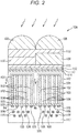
- Fig. 2 is a cross-section view schematically illustrating an exemplary configuration of the CMOS image sensor 10A. Additionally, a cross section of a part including two pixels is illustrated in the Figure, but other pixels basically have the same configuration.
- n-type well layers 101 are formed in a p-type semiconductor substrate 107 to be separated in an island shape per pixel.
- a photodiode configuring a pixel is formed in an n-type well layer 101.
- a fixed charge film 114, a transmissivity/refractivity adjustment layer 113, a passivation layer 112, and a transmissivity/refractivity adjustment layer 111 are laminated on the semiconductor substrate 107, and color filters 109 and 110 of colors corresponding to each pixel are further formed thereon.
- On-chip lenses 108 are formed on the color filters 109 and 110 via a planarization layer 118.
- a fixed charge film 115 and an insulating layer 117 are laminated below the semiconductor substrate 107, and metal wiring layers 116 are formed in the insulating layer 117.
- Each metal wiring layer 116 is insulated by the insulating layer 117.
- the CMOS image sensor 10A is a solid-state image sensing device of backside irradiation type for irradiating a light on the semiconductor substrate 107 provided with the wirings from the backside opposite to the top side.
- the backside of the semiconductor substrate 107 will be also called upper face and the top side of the semiconductor substrate 107 will be also called lower face in the following.
- a plurality of avalanche photodiode structures each including n+ region 102/avalanche region 104/p+ region 103 are repeatedly formed in one pixel.
- the n+ regions 102, the p+ regions 103, and the avalanche regions 104 are formed to extend in the thickness direction (vertically in Fig. 2 ) of the semiconductor substrate 107 within an n+ well layer 101.
- an avalanche region 104 is sandwiched between an n+ region 102 and a p+ region 103 thereby to configure an avalanche photodiode.
- an n+ region 102 or a p+ region 103 is shared between the adjacent structures each including n+ region 102/avalanche region 104/p+ region 103.
- a total of four avalanche regions 104 can be provided in the presence of three n+ regions 102 and the two p+ regions 103.
- An n+ region 102 is connected to an electrode (cathode electrode) 105 formed in the lower insulating layer 117 via a wiring or the like (not illustrated) .
- a p+ region 103 is connected to an electrode (anode electrode) 106 formed in the lower insulating layer 117 via a wiring or the like (not illustrated) .
- Each electrode 105 is connected at a different part from the cross section of Fig. 2 , and is set at the same potential. The electrodes 106 are similarly connected and set.
- the heights of the upper faces of the n+ regions 102, the p+ regions 103, and the avalanche regions 104 configuring an avalanche photodiode are almost the same, and the upper faces are covered with the n+ well layer 101 and the semiconductor substrate 107.
- Fig. 3 illustrates a horizontal cross-section view along the line A-A in Fig. 2 .
- the horizontal direction in Fig. 3 corresponds to the horizontal direction in Fig. 2
- the vertical direction corresponds to a direction perpendicular to the sheet of Fig. 2 .
- n+ regions 102, the p+ regions 103, and the avalanche regions 104 configuring an avalanche photodiode are formed to extend in parallel with each other in both the cross section of Fig. 2 and the cross section of Fig. 3 .
- a relationship between a voltage (potential difference) given to the n+ regions 102 and the p+ regions 103 and an electric field to be formed is determined by the width of the avalanche region 104 in Fig. 2 and Fig. 3 .
- a required voltage can be made smaller.
- the width of the avalanche region 104 is set between 0.05 ⁇ m and 1 pm, for example.
- n-type or p-type impurity-doped silicon can be used for the semiconductor substrate 107.
- Ge, GaAs, InP, GaP, InAs, GaSb, and InSb as well as semiconductor materials with wider band gap including three elements or four elements can be used.
- the avalanche region 104 is configured of a low-concentration impurity (n type or p type)-doped region, or a non-doped region.
- the n+ regions 102, the p+ regions 103, and the avalanche regions 104 configuring an avalanche photodiode can be formed by ion-implanting n-type impurity or p-type impurity into an n-type well layer 101 formed in each pixel by use of a mask corresponding to a pattern of each region.
- the fixed charge films 114 and 115 include a film with positive or negative fixed charges.
- the fixed charge films 114 and 115 are configured of a metal oxide film including oxide of aluminum, tantalum, zirconium, hafnium, yttrium, lanthanoid, or the like, or a metal nitride film including nitride of the above substances.
- the fixed charge films 114 and 115 are configured of a mix crystal-based film of oxide and nitride of the above substances.
- the avalanche regions 104 are formed to extend in the thickness direction of the semiconductor substrate 107 as described above, and thus the depth of the avalanche regions 104 can be set depending on a wavelength of a light to be detected. Further, an incident light is sufficiently absorbed thereby to generate many carriers from photons due to avalanche multiplication.
- a plurality of avalanche photodiode structures are repeatedly formed in one pixel, and thus the width of an avalanche region 104 between an n+ region 102 and a p+ region 103 can be reduced to be half or less than only one structure is employed. Consequently, an application voltage required for causing avalanche multiplication can be reduced. Thereby, the avalanche photodiodes can be applied also to a CMOS image sensor with relatively low drive voltage.
- a required application voltage is reduced thereby to restrict crosstalk with adjacent pixel or heat from being generated.
- a thick insulating isolation region or Peltier device does not need to be provided, thereby realizing finer pixels of the solid-state image sensing device in the CMOS image sensor 10A.
- the heights of the upper faces of the n+ regions 102, the p+ regions 103, and the avalanche regions 104 configuring an avalanche photodiode are almost the same, and thus almost-uniform electric fields are applied to the entire avalanche regions 104.
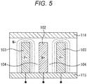
- the fixed charge films 114 and 115 are provided thereby to prevent a fall voltage of the avalanche photodiode from being varied, or a dark current from being generated. This point will be described with reference to Fig. 4 and Fig. 5 .
- Fig. 4 schematically illustrates a distribution of electric fields around the P+ regions 103 in an avalanche photodiode in a case where the fixed charge films 114 and 115 are not provided.
- Fig. 5 schematically illustrates a distribution of electric fields around the P+ regions 103 in an avalanche photodiode in a case where the fixed charge films 114 and 115 are provided. Additionally, the dotted lines around the p+ regions 103 in Fig. 4 and Fig. 5 indicate an equipotential line. Further, the n-type well layer 101 is not illustrated in Fig. 4 and Fig. 5 .
- the fixed charge films 114 and 115 are provided so that concentration of electric fields on the top side or backside of the semiconductor substrate 107 can be alleviated. Consequently, an influence due to the edge effect of the avalanche photodiode, the fringe effect of the avalanche photodiode, and the like is restricted.
- the fall voltage of the avalanche photodiode is stabilized and uniformly distributed. That is, the fall voltage at each position of the avalanche photodiode (each position particularly in the depth direction) is almost constant. Consequently, a reduction in light receiving sensitivity of the avalanche photodiodes can be prevented.
- the countermeasure that a low-concentration region is provided to alleviate an impurity concentration gradient, and the like are not made, and thus a reduction in light receiving sensitivity does not occur.
- a CMOS image sensor 10B as a second embodiment of the CMOS image sensor 10 of Fig. 1 will be described below with reference to Fig. 6 .
- Fig. 6 is a cross-section view schematically illustrating an exemplary configuration of the CMOS image sensor 10B. Additionally, the same reference numerals are denoted to the parts corresponding to those in Fig. 2 .
- the CMOS image sensor 10B is different from the CMOS image sensor 10A of Fig. 2 in that insulating films 119 and 120 are added.
- the insulating film 119 is formed between the semiconductor substrate 107 and the fixed charge film 114.
- the insulating film 120 is formed between the semiconductor substrate 107 and the fixed charge film 115.
- the insulating film 119 is arranged between the semiconductor substrate 107 and the fixed charge film 114 in this way, thereby preventing the avalanche photodiodes and the fixed charge film 114 from being electrically short-circuited in a case where the fixed charge film 114 is conductive.
- the insulating film 120 is arranged between the semiconductor substrate 107 and the fixed charge film 115, thereby preventing the avalanche photodiodes and the fixed charge film 115 from being electrically short-circuited in a case where the fixed charge film 115 is conductive.
- a CMOS image sensor 10C as a third embodiment of the CMOS image sensor 10 of Fig. 1 will be described below with reference to Fig. 7 to Fig. 9 .
- Fig. 7 is a cross-section view schematically illustrating an exemplary configuration of the CMOS image sensor 10C. Additionally, the same reference numerals are denoted to the parts corresponding to those in Fig. 2 .
- the CMOS image sensor 10C is different from the CMOS image sensor 10A of Fig. 2 in that fixed charge films 114a and 114b are formed instead of the fixed charge film 114 and fixed charge films 115a and 115b are formed instead of the fixed charge film 115.
- the fixed charge films 114a and 114b are formed in the same layer as the fixed charge film 114 in the CMOS image sensor 10A of Fig. 2 . However, the fixed charge film 114a is formed only near (above) the n+ regions 102. The fixed charge film 114b is formed only near (above) the p+ regions 103. The fixed charge films 114a and 114b are not formed in the inter-pixel parts where the n+ regions 102 and the p+ regions 103 are not formed.
- the fixed charge film 115a and 115b are formed in the same layer as the fixed charge film 115 in the CMOS image sensor 10B of Fig. 2 . However, the fixed charge film 115a is formed only near (below) the n+ regions 102. The fixed charge film 115b is formed only near (below) the p+ regions 103. The fixed charge films 115a and 115b are not formed in the inter-pixel parts where the n+ regions 102 and the p+ regions 103 are not formed.
- the fixed charge film 114a and the fixed charge film 115a include the same material, and have the same fixed charges .
- the fixed charge film 114b and the fixed charge film 115b include a different material from the fixed charge film 114a and the fixed charge film 115a, and have different fixed charges from the fixed charge film 114a and the fixed charge film 115a. Therefore, the fixed charges of the fixed charge films are different between near the n+ regions 102 and near the p+ regions 103.
- any of the exemplary materials of the fixed charge films 114 and 115 of Fig. 2 is employed for the fixed charge films 114a, 114b, 115a, and 115b, for example.
- the fixed charge films with different fixed charges are appropriately arranged depending on the layout of the n+ regions 102 and the p+ regions 103, thereby appropriately alleviating concentration of electric fields.
- a fixed charge film does not necessarily need to be provided in an inter-pixel part where concentration of electric fields does not need to be alleviated.
- an insulating film may be provided between the semiconductor substrate 107 and the fixed charge films 114a and 114b as well as between the semiconductor substrate 107 and the fixed charge films 115a and 115b in the CMOS image sensor 10C similarly as in the CMOS image sensor 10B of Fig. 6 .
- Fig. 8 and Fig. 9 illustrate only the parts required for explaining the method for manufacturing the fixed charge films 114a and 114b. Further, the n-type well layer 101 is not illustrated.
- a silicon oxide (SiO2) film 201 is formed on the upper face of the semiconductor substrate 107.
- the silicon oxide film 201 is patterned. Thereby, openings 201A are formed in the silicon oxide film 201 above the p+ regions 103.
- the fixed charge film 114b is formed on the upper face of the semiconductor substrate 107 and the upper face of the silicon oxide film 201. At this time, the fixed charge film 114b is embedded in the openings 201A in the silicon oxide film 201.
- the fixed charge film 114b is polished by chemical mechanical polishing (CMP) . Thereby, the fixed charge film 114b other than in the openings 201A in the silicon oxide film 201 is removed.
- CMP chemical mechanical polishing
- the silicon oxide film 201 is patterned. Thereby, opening 201B are formed in the silicon oxide film 201 above the n+ regions 102.
- the fixed charge film 114a is formed on the upper face of the semiconductor substrate 107 and the upper face of the silicon oxide film 201. At this time, the fixed charge film 114a is embedded in the openings 201B in the silicon oxide film 201.
- the fixed charge film 114a is polished by CMP. Thereby, the fixed charge film 114a other than in the openings 201B in the silicon oxide film 201 is removed.
- the fixed charge films 114a and 114b are formed in this way.
- Fig. 10 illustrates a first variant of the horizontal cross-section view along the line A-A in Fig. 2 .
- the horizontal direction in Fig. 10 corresponds to the horizontal direction in Fig. 2
- the vertical direction corresponds to a direction perpendicular to the sheet of Fig. 2 similarly as in Fig. 3 .
- the n+ regions 102 include n+ regions 102A and 102B.
- the avalanche regions 104 include avalanche regions 104A and 104B.
- the n+ region 102A is a columnar region with a circular cross section, and is arranged at the center of a pixel.
- the n+ region 102B, the p+ region 103, and the avalanche regions 104A and 104B are cylindrical regions with a circle-framed cross section.
- the avalanche region 104A, the p+ region 103, the avalanche region 104B, and the n+ region 102B are then arranged from the inside in this order such that each region concentrically surrounds the n+ region 102A.
- Fig. 11 illustrates a horizontal cross-section view along the line B-B in Fig. 2 .
- the horizontal direction in Fig. 11 corresponds to the horizontal direction in Fig. 2
- the vertical direction corresponds to a direction perpendicular to the sheet of Fig. 2 similarly as in Fig. 3 and Fig. 10 .
- the electrodes 105 include an electrode 105A, a connection part 105B, and an electrode 105C.
- the electrodes 106 include an electrode 106A and a connection part 106B.
- the cross section of the electrode 105A has a substantially similar shape to the n+ region 102A in Fig. 10 , and is connected to the n+ region 102A via a wiring or the like (not illustrated) .
- the cross section of the electrode 105C is an arc-shaped region along the bottom (circular frame) of the n+ region 102B in Fig. 10 , and is connected to the n+ region 102B via a wiring or the like (not illustrated). Further, the electrode 105C is formed with a discontinuous part 105D where part of the arc is discontinuous .
- the cross section of the electrode 106A is an arc-shaped region along the bottom (circular frame) of the p+ region 103 in Fig. 10 , and is connected to the p+ region 103 via a wiring or the like (not illustrated) . Further, the electrode 106A is formed with a discontinuous part 106C where part of the arc is discontinuous.
- the electrode 105A and the electrode 105C are connected via the connection part 105B with a linear cross section through the discontinuous part 106C in the electrode 106A.
- the electrode 106A is connected to a wiring or the like (not illustrated) at the circumferential edge of the pixel through the discontinuous part 105D in the electrode 105C via the connection part 106B with a linear cross section.
- electric fields easily occur near the discontinuous part 105D in the electrode 105C at the lower end of the n+ region 102B connected to the electrode 105C. Further, electric fields easily occur near the discontinuous part 106C in the electrode 106A at the lower end of the p+ region 103 connected to the electrode 106A.
- the fixed charge film 115 may be arranged only in a region 301 and a region 302 surrounded in dotted lines in Fig. 11 between the semiconductor substrate 107 and the insulating layer 117. Additionally, the region 301 coverts at least above the discontinuous part 106C. The region 302 coverts at least above the discontinuous part 105D.
- the fixed charges of the fixed charge film 115 may be changed between the region 301 and the region 302 depending on a difference in polarity between the p+ region 103 and the n+ region 102B.
- the material of the fixed charge film 115 may be changed between the regions 301, 302 and other regions.
- Fig. 12 illustrates a second variant of the horizontal cross-section view along the line A-A in Fig. 2 .
- the horizontal direction in Fig. 12 corresponds to the horizontal direction in Fig. 2
- the vertical direction corresponds to a direction perpendicular to the sheet of Fig. 2 similarly as in Fig. 3 .
- the n+ regions 102 include n+ regions 102A and 102B.
- the avalanche regions 104 include avalanche regions 104A and 104B.
- the n+ region 102A is a quadrangular-prism-shaped region with a rectangular cross section, and is arranged at the center of a pixel.
- the n+ region 102B, the p+ region 103, and the avalanche regions 104A and 104B are quadrangular-prism-shaped regions with a rectangular-framed cross section.
- the avalanche region 104A, the p+ region 103, the avalanche region 104B, and the n+ region 102B are then arranged from the inside in this order such that each region surrounds the n+ region 102A in a frame shape.
- the fixed charge films 114 and 115 may be arranged only in regions 321a to 321d and regions 322a to 322d surrounded in dotted lines in Fig. 11 . Additionally, the regions 321a to 321d cover at least near the corners of the n+ region 102A. The regions 322a to 322d cover at least near the corners of the p+ region 103.
- the fixed charges of the fixed charge film 114 may be changed between the regions 321a to 321d and the regions 322a to 322d depending on a difference in polarity between the n+ region 102A and the p+ region 102B.
- the fixed charges of the fixed charge film 115 may be changed between the regions 321a to 321d and the regions 322a to 322d.
- the material of the fixed charge films 114 and 115 may be changed between the regions 321a to 321d and the regions 322a to 322d.
- the outermost region in an avalanche photodiode structure in each pixel is limited to the n+ region 102B. Therefore, the outermost regions in adjacent pixels are of the same conductive type, and insulating isolation between the pixels is facilitated.
- the plane pattern of the n+ regions 102, the p+ regions 103, and the avalanche regions 104 configuring an avalanche photodiode is not limited to the above example, and may be other plane pattern. As in the examples in Fig. 3 , Fig. 10 , and Fig. 12 , however, it is preferable to repeat a simple-shape pattern.
- a simple-shape pattern enables a margin corresponding to mask offset in ion implantation to be secured, thereby easily decreasing the pattern width and lowering the voltage.
- the n+ regions 102 and the p+ regions 103 may be arranged in a reverse way to the above example. Further, for example, the number of repetitions of the n+ regions 102, the p+ regions 103, and the avalanche regions 104 may be increased or decreased.
- the fixed charge films may be arranged to cover at least around each discontinuous part.
- the fixed charge films may be arranged to cover at least around each discontinuous part.
- the fixed charge films may be arranged to cover at least around the corners of each region similarly as in the examples described with reference to Fig. 12 and Fig. 13 .
- the present technology is applied to a CMOS image sensor in which unit pixels are arranged in a matrix shape, but the present technology is not limited to the CMOS image sensor. That is, the present technology is applicable to general solid-state image sensing devices including avalanche photodiodes extending in the thickness direction of a semiconductor substrate.
- the present technology is applicable to solid-state image sensing devices of backside irradiation type.
- the above description demonstrates the example in which the fixed charge films are provided on both the top side and the backside of the semiconductor substrate, but a fixed charge film may be provided on either side.
- a solid-state image sensing device to which the present technology is applied may be formed as one chip, or may be in a module shape having an imaging function in which an imaging unit, and a signal processing unit or an optical system are collectively packaged.
- Fig. 14 is a diagram illustrating exemplary use of the above solid-state image sensing devices.
- the above solid-state image sensing devices can be used in various cases for sensing a visible ray, an infrared ray, an ultraviolet ray, an X ray, and the like as described below, for example.
- Fig. 15 is a block diagram illustrating an exemplary configuration of a shooting device (camera device) as an exemplary electronic device to which the present technology is applied.
- a shooting device includes an optical system including a group of lenses 501 and the like, an imaging device 502, a DSP circuit 503 as camera signal processing unit, a frame memory 504, a display device 505, a recording device 506, an operation system 507, a power supply system 508, and the like. Furthermore, the DSP circuit 503, the frame memory 504, the display device 505, the recording device 506, the operation system 507, and the power supply system 508 are mutually connected via a bus line 509.
- the group of lenses 501 takes an incident light (image light) from a subject and forms an image on an imaging face of the imaging device 502.
- the imaging device 502 converts the amount of incident light formed on the imaging face by the group of lenses 501 into an electric signal in units of pixel, and outputs the electric signal as pixel signal.
- the display device 505 is configured of a panel-type display device such as liquid crystal display device or electro luminescence (EL) display device, and displays an animation or still image shot by the imaging device 502.
- the recording device 506 records the animation or still image shot by the imaging device 502 in a recording medium such as memory card, video tape, or digital versatile disk (DVD).
- the operation system 507 issues operation instructions to various functions in the shooting device in response to user' s operations .
- the power supply system 508 supplies power to various power supplies as operation power supplies of the DSP circuit 503, the frame memory 504, the display device 505, the recording device 506, and the operation system 507 as needed.
- the shooting device is applied to camera modules for mobile devices such as video camera, digital still camera, Smartphone, and cell phone. Then, a solid-state image sensing device according to each embodiment can be used as the imaging device 502 in the shooting device. Thereby, image quality of the shooting device can be enhanced.
- the present technology can employ the following configurations, for example.
Landscapes
- Engineering & Computer Science (AREA)
- Multimedia (AREA)
- Signal Processing (AREA)
- Solid State Image Pick-Up Elements (AREA)
- Transforming Light Signals Into Electric Signals (AREA)
- Light Receiving Elements (AREA)
Abstract
Description
- The present technology relates to a solid-state image sensing device, an electronic device, and a method for manufacturing the solid-state image sensing device, and particularly to a solid-state image sensing device using avalanche multiplication, an electronic device, and a method for manufacturing the solid-state image sensing device.
- In recent years, a pixel size has been reduced in order to realize smaller and finer solid-state image sensing devices. When an image size is reduced, however, not only a light receiving area of a photodiode as light receiving device but also a volume of a region for photoelectric conversion is reduced, and thus a light receiving efficiency lowers.
- On the other hand, higher sensitivity of solid-state image sensing devices is desired in order to shoot an image with high image quality even in a state with less incident light, such as shooting a dark place or detecting a slight amount of radiation.
- To the contrary, there is proposed a solid-state image sensing device using avalanche photodiodes by use of avalanche multiplication in order to achieve both downsizing and higher sensitivity (see Patent Document 1, for example).
- Patent Document 1: Japanese Patent Application Laid-Open No.
2010-157665 - Incidentally, in an avalanche photodiode driven in a Geiger mode, a bias voltage near a fall voltage of a diode is applied thereby to have sensitivity to single photons. Thus, the fall voltage of a diode is an important parameter.
- On the other hand, a curvature of an electric field intensity is higher at an end of a pn junction in an avalanche photodiode, and the fall voltage lowers. This is a phenomenon called edge effect or fringe effect. For example, according to the invention described in Patent Document 1, an end of a pn junction is present on a surface of a semiconductor substrate on which an avalanche photodiode is formed. Consequently, outward diffusion or pile-up of impurities easily occurs on the surface of the semiconductor substrate, and the fall voltage lowers.
- Then, if a bias voltage is applied according to a region where the fall voltage lowers, for example, only a lower voltage than the fall voltage is applied in other regions. Consequently, light receiving sensitivity of avalanche photodiodes lowers.
- To the contrary, it has been conventionally proposed that a low-concentration region is provided to alleviate an impurity concentration gradient and the like. However, if a low-concentration region is formed near a surface of the semiconductor substrate, light receiving sensitivity to short-wavelength incident lights lowers.
- The present technology has been made in terms of the situations, and is directed for preventing a reduction in light receiving sensitivity of avalanche photodiodes.
- A solid-state image sensing device according to a first aspect of the present technology includes an avalanche photodiode having a first region of a first conductive type, a second region of a second conductive type different from the first conductive type, and an avalanche region sandwiched between the first region and the second region, which extend in a thickness direction of a semiconductor substrate, and a film formed on at least one side of the semiconductor substrate and including a metal oxide film, a metal nitride film, or a mix crystal-based film of metal oxide film and metal nitride film.
- An insulating film formed between the film and the semiconductor substrate can be further provided.
- The film can include an oxide film or nitride film of aluminum, tantalum, zirconium, hafnium, yttrium, or lanthanoid, or a mix crystal-based film of oxide and nitride of aluminum, tantalum, zirconium, hafnium, yttrium, or lanthanoid.
- The film can have fixed charges.
- The film can have different fixed charges between near the first region and near the second region.
- In a case where the first region is in a rectangular tube shape, the film can be formed to cover at least around corners of the first region.
- The first region is cylindrical, an electrode formed along the upper face or the bottom face of the first region and having one or more discontinuous parts can be further provided on one side of the semiconductor substrate, and the film can be formed to cover at least around the discontinuous parts in the electrode between the semiconductor substrate and the electrode.
- Two or more avalanche photodiode structures can be repeatedly formed in one pixel.
- A method for manufacturing a solid-state image sensing device according to a second aspect of the present technology includes a step of forming a film including a metal oxide film, a metal nitride film, or a mix crystal-based film of metal oxide film and metal nitride film on at least one side of a semiconductor substrate on which an avalanche photodiode having a first region of a first conductive type, a second region of a second conductive type different from the first conductive type, and an avalanche region sandwiched between the first region and the second region, which extend in a thickness direction of the semiconductor substrate, is formed.
- An electronic device according to a third aspect of the present technology includes a solid-state image sensing device, and a signal processing unit for processing a signal output from the solid-state image sensing device, in which the solid-state image sensing device includes an avalanche photodiode having a first region of a first conductive type, a second region of a second conductive type different from the first conductive type, and an avalanche region sandwiched between the first region and the second region, which extend in a thickness direction of a semiconductor substrate, and a film formed on at least one side of the semiconductor substrate and including a metal oxide film, a metal nitride film, or a mix crystal-based film of metal oxide film and metal nitride film.
- According to the first or third aspect of the present technology, a film including a metal oxide film, a metal nitride film, or a mix crystal-based film of metal oxide film and metal nitride film, which is formed on at least one side of a semiconductor substrate, enables a variation in fall voltage or an occurrence in dark current in an avalanche photodiode to be restricted.
- According to the second aspect of the present technology, a film including a metal oxide film, a metal nitride film, or a mix crystal-based film of metal oxide film and metal nitride film is formed on at least one side of a semiconductor substrate on which an avalanche photodiode having a first region of a first conductive type, a second region of a second conductive type different from the first conductive type, and an avalanche region sandwiched between the first region and the second region, which extend in a thickness direction of the semiconductor substrate, is formed.
- According to the first to third aspects of the present technology, it is possible to prevent a reduction in light receiving sensitivity of avalanche photodiodes.
- Additionally, the effects described in the present specification are merely exemplary, and the effects of the present technology are not limited to the effects described in the present specification, and additional effects may be obtained.
-
-
Fig. 1 is a block diagram illustrating an exemplary schematic configuration of a CMOS image sensor to which the present technology is applied. -
Fig. 2 is a cross-section view illustrating a first embodiment of the CMOS image sensor. -
Fig. 3 is a diagram illustrating an exemplary plane pattern of an avalanche photodiode. -
Fig. 4 is a diagram schematically illustrating a distribution of electric fields in an avalanche photodiode in a case where fixed charge films are not provide. -
Fig. 5 is a diagram schematically illustrating a distribution of electric fields in an avalanche photodiode in a case where fixed charge films are provided. -
Fig. 6 is a cross-section view illustrating a second embodiment of the CMOS image sensor. -
Fig. 7 is a cross-section view illustrating a third embodiment of the CMOS image sensor. -
Fig. 8 is a diagram for explaining a method for manufacturing a fixed charge film of the CMOS image sensor ofFig. 7 . -
Fig. 9 is a diagram for explaining the method for manufacturing a fixed charge film of the CMOS image sensor ofFig. 7 . -
Fig. 10 is a diagram illustrating a first variant of the plane pattern of an avalanche photodiode. -
Fig. 11 is a diagram illustrating an exemplary region in which fixed charge films are arranged for the avalanche photodiode ofFig. 10 . -
Fig. 12 is a diagram illustrating a second variant of the plane pattern of an avalanche photodiode. -
Fig. 13 is a diagram illustrating an exemplary region in which fixed charge films are arranged for the avalanche photodiode ofFig. 12 . -
Fig. 14 is a diagram illustrating exemplary use of solid-state image sensing devices. -
Fig. 15 is a block diagram illustrating an exemplary configuration of an electric device to which the present technology is applied. - Modes for carrying out the present technology (which will be denoted as embodiments below) will be describedbelow. Additionally, the description will be made in the following order.
- 1. Solid-state image sensing device to which the present technology is applied
- 2. First embodiment
- 3. Second embodiment (example in which insulating films are provided)
- 4. Third embodiment (example in which fixed charge films with different fixed charges are provided)
- 5. Variants
- 6. Exemplary use of solid-state image sensing devices
-
Fig. 1 is a system configuration diagram illustrating a schematic configuration of a solid-state image sensing device to which the present technology is applied, such as a CMOS image sensor as a kind of solid-state image sensing device of X-Y address system. Here, the CMOS image sensor is created by applying a CMOS process or using part of it. - A
CMOS image sensor 10 according to the present application is configured of apixel array part 11 formed on a semiconductor substrate 107 (Fig. 2 ), and peripheral circuit units integrated on thesame semiconductor substrate 107 as thepixel array part 11. The peripheral circuit units are configured of avertical drive unit 12, acolumn processing unit 13, ahorizontal drive unit 14, and asystem control unit 15, for example. - The
CMOS image sensor 10 further includes asignal processing unit 18 and adata storage unit 19. Thesignal processing unit 18 and thedata storage unit 19 may be mounted on the same substrate as theCMOS image sensor 10, or may be arranged on a different substrate from theCMOS image sensor 10. Further, each processing of thesignal processing unit 18 and thedata storage unit 19 may be performed by an external signal processing unit provided on a different substrate from theCMOS image sensor 10, such as digital signal processor (DSP) circuit or software. - The
pixel array part 11 is configured such that a plurality of unit pixels (which will be simply denoted as "pixel" below) are arranged in a row direction and in a column direction. Here, the row direction is a direction in which the pixels in the pixel rows are arranged (or horizontal direction), and the column direction is a direction in which the pixels in the pixel columns are arranged (or vertical direction). - A unit pixel has a photoelectric conversion unit (such as photodiode) for generating and accumulating charges depending on the amount of received light, and a plurality of pixel transistors (or MOS transistors). The plurality of pixel transistors can be configured of three transistors including a transfer transistor, a reset transistor, and an amplification transistor, for example. Alternatively, the plurality of pixel transistors can be configured of the four transistors including a select transistor. Additionally, an equivalent circuit of each pixel is similar to a general one, and a detailed description thereof will be omitted here.
- Further, a unit pixel can be in a common pixel structure. The common pixel structure is configured of a plurality of photoelectric conversion units, a plurality of transfer transistors, one shared floating diffusion, and each of the other shared pixel transistors.
- In the
pixel array part 11,pixel drive lines 16 as row signal lines are arranged in the row direction for the pixel rows, respectively, andvertical signal lines 17 as column signal lines are arranged in the column direction for the pixel columns, respectively. Thepixel drive lines 16 transmit a drive signal for driving when reading a signal from a pixel. Thepixel drive lines 16 are illustrated as one wiring inFig. 1 , but are not limited to one. An end of apixel drive line 16 is connected to an output terminal corresponding to each row of thevertical drive unit 12. - The
vertical drive unit 12 is configured of a shift register, address decoder, or the like, and drives all the pixels in thepixel array part 11 at the same time, in units of row, or the like. That is, thevertical drive unit 12 configures a drive unit for controlling the operations of each pixel in thepixel array part 11 together with thesystem control unit 15 for controlling thevertical drive unit 12. A specific configuration of thevertical drive unit 12 is not illustrated, but generally has two scanning systems of read scanning system and sweep scanning system. - The read scanning system selects and scans the unit pixels in the
pixel array part 11 in units of row in order to read a signal from a unit pixel. The signal read from a unit pixel is an analog signal. The sweep scanning system sweeps and scans the read rows on which the read scanning system performs read scanning earlier than the read scanning by an exposure time. - Unnecessary charges are swept from the photoelectric conversion unit in a unit pixel in the read row in the sweep scanning by the sweep scanning system thereby to reset the photoelectric conversion unit. Unnecessary charges are then swept (reset) by the sweep scanning system so that an electronic shutter operation is performed. Here, the electronic shutter operation is an operation of discarding charges in the photoelectric conversion unit and newly starting exposure (starting accumulating charges) .
- A signal read in the read operation by the read scanning system corresponds to the amount of light received after the previous read operation or the electronic shutter operation. Then, a period from a read timing by a previous read operation or a sweep timing by the electronic shutter operation to a read timing by a current read operation is a charge exposure period in the unit pixel.
- A signal output from each unit pixel in a pixel row selected and scanned by the
vertical drive unit 12 is input into thecolumn processing unit 13 via each of thevertical signal lines 17 per column of pixels. Thecolumn processing unit 13 performs a predetermined signal processing on the signal output from each pixel in a selected row via thevertical signal lines 17 and temporarily holds the signal-processed pixel signal per column of pixels in thepixel array part 11. - Specifically, the
column processing unit 13 performs at least a noise cancelation processing such as correlated double sampling (CDS) processing or double data sampling (DDS) processing as signal processing. For example, reset noises, or pixel-specific fixed pattern noises such as threshold variation of the amplification transistor in a pixel are canceled by the CDS processing. Thecolumn processing unit 13 can have an analog-digital (AD) conversion function, for example, in addition to the noise cancelation processing, and can convert an analog pixel signal into a digital signal and output the digital signal. - The
horizontal drive unit 14 is configured of a shift register, address decoder, or the like, and selects a unit circuit corresponding to a pixel column in thecolumn processing unit 13 in turn. With the selecting and scanning by thehorizontal drive unit 14, a pixel signal signal-processed per unit circuit in thecolumn processing unit 13 is output in turn. - The
system control unit 15 is configured of a timing generator or the like for generating various timing signals, and controls driving thevertical drive unit 12, thecolumn processing unit 13, thehorizontal drive unit 14, and the like on the basis of the timings generated by the timing generator. - The
signal processing unit 18 has at least a calculation processing function, and performs various types of signal processing such as calculation processing on a pixel signal output from thecolumn processing unit 13. Thedata storage unit 19 temporarily stores data required for the signal processing in thesignal processing unit 18. - A
CMOS image sensor 10A as a first embodiment of theCMOS image sensor 10 ofFig. 1 will be described below with reference toFig. 2 to Fig. 4 . -
Fig. 2 is a cross-section view schematically illustrating an exemplary configuration of theCMOS image sensor 10A. Additionally, a cross section of a part including two pixels is illustrated in the Figure, but other pixels basically have the same configuration. - In the
CMOS image sensor 10A, n-type well layers 101 are formed in a p-type semiconductor substrate 107 to be separated in an island shape per pixel. A photodiode configuring a pixel is formed in an n-type well layer 101. - A fixed
charge film 114, a transmissivity/refractivity adjustment layer 113, apassivation layer 112, and a transmissivity/refractivity adjustment layer 111 are laminated on thesemiconductor substrate 107, andcolor filters - On-
chip lenses 108 are formed on thecolor filters planarization layer 118. - On the other hand, a fixed
charge film 115 and an insulatinglayer 117 are laminated below thesemiconductor substrate 107, and metal wiring layers 116 are formed in the insulatinglayer 117. Eachmetal wiring layer 116 is insulated by the insulatinglayer 117. - In the
CMOS image sensor 10A, the insulatinglayer 117 provided with the metal wiring layers 116 is formed on the opposite side to thecolor filters chip lenses 108 across thesemiconductor substrate 107 forming the photodiodes therein. That is, theCMOS image sensor 10A is a solid-state image sensing device of backside irradiation type for irradiating a light on thesemiconductor substrate 107 provided with the wirings from the backside opposite to the top side. - Additionally, the backside of the
semiconductor substrate 107 will be also called upper face and the top side of thesemiconductor substrate 107 will be also called lower face in the following. - According to the present embodiment, particularly a plurality of avalanche photodiode structures each including
n+ region 102/avalanche region 104/p+ region 103 are repeatedly formed in one pixel. Specifically, then+ regions 102, thep+ regions 103, and theavalanche regions 104 are formed to extend in the thickness direction (vertically inFig. 2 ) of thesemiconductor substrate 107 within ann+ well layer 101. Then, anavalanche region 104 is sandwiched between ann+ region 102 and ap+ region 103 thereby to configure an avalanche photodiode. - Further, as illustrated in
Fig. 2 , ann+ region 102 or ap+ region 103 is shared between the adjacent structures each includingn+ region 102/avalanche region 104/p+ region 103. Thereby, a total of fouravalanche regions 104 can be provided in the presence of threen+ regions 102 and the twop+ regions 103. - An
n+ region 102 is connected to an electrode (cathode electrode) 105 formed in the lower insulatinglayer 117 via a wiring or the like (not illustrated) . Ap+ region 103 is connected to an electrode (anode electrode) 106 formed in the lower insulatinglayer 117 via a wiring or the like (not illustrated) . Eachelectrode 105 is connected at a different part from the cross section ofFig. 2 , and is set at the same potential. Theelectrodes 106 are similarly connected and set. - Further, the heights of the upper faces of the
n+ regions 102, thep+ regions 103, and theavalanche regions 104 configuring an avalanche photodiode are almost the same, and the upper faces are covered with the n+ well layer 101 and thesemiconductor substrate 107. -
Fig. 3 illustrates a horizontal cross-section view along the line A-A inFig. 2 . The horizontal direction inFig. 3 corresponds to the horizontal direction inFig. 2 , and the vertical direction corresponds to a direction perpendicular to the sheet ofFig. 2 . - The
n+ regions 102, thep+ regions 103, and theavalanche regions 104 configuring an avalanche photodiode are formed to extend in parallel with each other in both the cross section ofFig. 2 and the cross section ofFig. 3 . - Further, a relationship between a voltage (potential difference) given to the
n+ regions 102 and thep+ regions 103 and an electric field to be formed is determined by the width of theavalanche region 104 inFig. 2 andFig. 3 . As the width of theavalanche region 104 is smaller, a required voltage can be made smaller. The width of theavalanche region 104 is set between 0.05 µm and 1 pm, for example. - n-type or p-type impurity-doped silicon can be used for the
semiconductor substrate 107. Further, Ge, GaAs, InP, GaP, InAs, GaSb, and InSb as well as semiconductor materials with wider band gap including three elements or four elements can be used. - The
avalanche region 104 is configured of a low-concentration impurity (n type or p type)-doped region, or a non-doped region. - For example, the
n+ regions 102, thep+ regions 103, and theavalanche regions 104 configuring an avalanche photodiode can be formed by ion-implanting n-type impurity or p-type impurity into an n-type well layer 101 formed in each pixel by use of a mask corresponding to a pattern of each region. - The fixed
charge films charge films charge films - The
avalanche regions 104 are formed to extend in the thickness direction of thesemiconductor substrate 107 as described above, and thus the depth of theavalanche regions 104 can be set depending on a wavelength of a light to be detected. Further, an incident light is sufficiently absorbed thereby to generate many carriers from photons due to avalanche multiplication. - Furthermore, a plurality of avalanche photodiode structures are repeatedly formed in one pixel, and thus the width of an
avalanche region 104 between ann+ region 102 and ap+ region 103 can be reduced to be half or less than only one structure is employed. Consequently, an application voltage required for causing avalanche multiplication can be reduced. Thereby, the avalanche photodiodes can be applied also to a CMOS image sensor with relatively low drive voltage. - Further, a required application voltage is reduced thereby to restrict crosstalk with adjacent pixel or heat from being generated. Thereby, a thick insulating isolation region or Peltier device does not need to be provided, thereby realizing finer pixels of the solid-state image sensing device in the
CMOS image sensor 10A. - On the other hand, with a comparison at the same application voltage, electric fields on the
avalanche regions 104 can be made stronger than in one structure, and the number of carriers generated per photon can be increased. Thereby, responsiveness to the low amount of light can be enhanced. Thus, an improvement in sensitivity to the low light level can be realized while a wide dynamic range is kept. - Further, the heights of the upper faces of the
n+ regions 102, thep+ regions 103, and theavalanche regions 104 configuring an avalanche photodiode are almost the same, and thus almost-uniform electric fields are applied to theentire avalanche regions 104. - Furthermore, the fixed
charge films Fig. 4 andFig. 5 . -
Fig. 4 schematically illustrates a distribution of electric fields around theP+ regions 103 in an avalanche photodiode in a case where the fixedcharge films Fig. 5 schematically illustrates a distribution of electric fields around theP+ regions 103 in an avalanche photodiode in a case where the fixedcharge films p+ regions 103 inFig. 4 andFig. 5 indicate an equipotential line. Further, the n-type well layer 101 is not illustrated inFig. 4 andFig. 5 . - As in the parts indicated by the arrows in
Fig. 4 , electric fields concentrate around the top side or backside of thesemiconductor substrate 107 due to the shape or depth of the pn junction end of the avalanche photodiode, and surface pile-up or outward diffusion/suction of impurities on thesemiconductor substrate 107. Consequently, a fall voltage of the avalanche photodiode varies or a dark current noise occurs around the top side or backside of thesemiconductor substrate 107. - On the other hand, as illustrated in
Fig. 5 , the fixedcharge films semiconductor substrate 107 can be alleviated. Consequently, an influence due to the edge effect of the avalanche photodiode, the fringe effect of the avalanche photodiode, and the like is restricted. - Thereby, the fall voltage of the avalanche photodiode is stabilized and uniformly distributed. That is, the fall voltage at each position of the avalanche photodiode (each position particularly in the depth direction) is almost constant. Consequently, a reduction in light receiving sensitivity of the avalanche photodiodes can be prevented.
- Further, the countermeasure that a low-concentration region is provided to alleviate an impurity concentration gradient, and the like are not made, and thus a reduction in light receiving sensitivity does not occur.
- Therefore, the avalanche photodiodes with high sensitivity to incident lights ranging short wavelength to long wavelength are realized.
- Further, a dark current is prevented from being generated around the top side and the backside of the
semiconductor substrate 107 due to the surface pinning effect of the fixedcharge films - A
CMOS image sensor 10B as a second embodiment of theCMOS image sensor 10 ofFig. 1 will be described below with reference toFig. 6 . -
Fig. 6 is a cross-section view schematically illustrating an exemplary configuration of theCMOS image sensor 10B. Additionally, the same reference numerals are denoted to the parts corresponding to those inFig. 2 . - The
CMOS image sensor 10B is different from theCMOS image sensor 10A ofFig. 2 in that insulatingfilms - The insulating
film 119 is formed between thesemiconductor substrate 107 and the fixedcharge film 114. The insulatingfilm 120 is formed between thesemiconductor substrate 107 and the fixedcharge film 115. - The insulating
film 119 is arranged between thesemiconductor substrate 107 and the fixedcharge film 114 in this way, thereby preventing the avalanche photodiodes and the fixedcharge film 114 from being electrically short-circuited in a case where the fixedcharge film 114 is conductive. Similarly, the insulatingfilm 120 is arranged between thesemiconductor substrate 107 and the fixedcharge film 115, thereby preventing the avalanche photodiodes and the fixedcharge film 115 from being electrically short-circuited in a case where the fixedcharge film 115 is conductive. - A CMOS image sensor 10C as a third embodiment of the
CMOS image sensor 10 ofFig. 1 will be described below with reference toFig. 7 to Fig. 9 . -
Fig. 7 is a cross-section view schematically illustrating an exemplary configuration of the CMOS image sensor 10C. Additionally, the same reference numerals are denoted to the parts corresponding to those inFig. 2 . - The CMOS image sensor 10C is different from the
CMOS image sensor 10A ofFig. 2 in that fixedcharge films charge film 114 and fixedcharge films charge film 115. - The fixed
charge films charge film 114 in theCMOS image sensor 10A ofFig. 2 . However, the fixedcharge film 114a is formed only near (above) then+ regions 102. The fixedcharge film 114b is formed only near (above) thep+ regions 103. The fixedcharge films n+ regions 102 and thep+ regions 103 are not formed. - The fixed
charge film charge film 115 in theCMOS image sensor 10B ofFig. 2 . However, the fixedcharge film 115a is formed only near (below) then+ regions 102. The fixedcharge film 115b is formed only near (below) thep+ regions 103. The fixedcharge films n+ regions 102 and thep+ regions 103 are not formed. - Further, the fixed
charge film 114a and the fixedcharge film 115a include the same material, and have the same fixed charges . The fixedcharge film 114b and the fixedcharge film 115b include a different material from the fixedcharge film 114a and the fixedcharge film 115a, and have different fixed charges from the fixedcharge film 114a and the fixedcharge film 115a. Therefore, the fixed charges of the fixed charge films are different between near then+ regions 102 and near thep+ regions 103. - Additionally, any of the exemplary materials of the fixed
charge films Fig. 2 is employed for the fixedcharge films - The fixed charge films with different fixed charges are appropriately arranged depending on the layout of the
n+ regions 102 and thep+ regions 103, thereby appropriately alleviating concentration of electric fields. - Additionally, as illustrated in
Fig. 7 , a fixed charge film does not necessarily need to be provided in an inter-pixel part where concentration of electric fields does not need to be alleviated. - Additionally, an insulating film may be provided between the
semiconductor substrate 107 and the fixedcharge films semiconductor substrate 107 and the fixedcharge films CMOS image sensor 10B ofFig. 6 . - A method for manufacturing the fixed
charge films Fig. 8 andFig. 9 . - Additionally,
Fig. 8 andFig. 9 illustrate only the parts required for explaining the method for manufacturing the fixedcharge films type well layer 101 is not illustrated. - At first, as illustrated in A of
Fig. 8 , a silicon oxide (SiO2)film 201 is formed on the upper face of thesemiconductor substrate 107. - Next, as illustrated in B of
Fig. 8 , thesilicon oxide film 201 is patterned. Thereby,openings 201A are formed in thesilicon oxide film 201 above thep+ regions 103. - Next, as illustrated in C of
Fig. 8 , the fixedcharge film 114b is formed on the upper face of thesemiconductor substrate 107 and the upper face of thesilicon oxide film 201. At this time, the fixedcharge film 114b is embedded in theopenings 201A in thesilicon oxide film 201. - Next, as illustrated in D of
Fig. 8 , the fixedcharge film 114b is polished by chemical mechanical polishing (CMP) . Thereby, the fixedcharge film 114b other than in theopenings 201A in thesilicon oxide film 201 is removed. - Next, as illustrated in E of
Fig. 9 , thesilicon oxide film 201 is patterned. Thereby, opening 201B are formed in thesilicon oxide film 201 above then+ regions 102. - Next, as illustrated in F of
Fig. 9 , the fixedcharge film 114a is formed on the upper face of thesemiconductor substrate 107 and the upper face of thesilicon oxide film 201. At this time, the fixedcharge film 114a is embedded in theopenings 201B in thesilicon oxide film 201. - Next, as illustrated in G of
Fig. 9 , the fixedcharge film 114a is polished by CMP. Thereby, the fixedcharge film 114a other than in theopenings 201B in thesilicon oxide film 201 is removed. - The fixed
charge films - Variants of the aforementioned embodiments of the present technology will be described below.
- Variants of the plane pattern of the
n+ regions 102, thep+ regions 103, and theavalanche regions 104 configuring an avalanche photodiode will be first described with reference toFig. 10 to Fig. 13 . -
Fig. 10 illustrates a first variant of the horizontal cross-section view along the line A-A inFig. 2 . The horizontal direction inFig. 10 corresponds to the horizontal direction inFig. 2 , and the vertical direction corresponds to a direction perpendicular to the sheet ofFig. 2 similarly as inFig. 3 . - In the example, the
n+ regions 102 includen+ regions avalanche regions 104 includeavalanche regions - The
n+ region 102A is a columnar region with a circular cross section, and is arranged at the center of a pixel. Then+ region 102B, thep+ region 103, and theavalanche regions avalanche region 104A, thep+ region 103, theavalanche region 104B, and then+ region 102B are then arranged from the inside in this order such that each region concentrically surrounds then+ region 102A. -
Fig. 11 illustrates a horizontal cross-section view along the line B-B inFig. 2 . The horizontal direction inFig. 11 corresponds to the horizontal direction inFig. 2 , and the vertical direction corresponds to a direction perpendicular to the sheet ofFig. 2 similarly as inFig. 3 andFig. 10 . - The
electrodes 105 include anelectrode 105A, a connection part 105B, and an electrode 105C. Theelectrodes 106 include anelectrode 106A and aconnection part 106B. - The cross section of the
electrode 105A has a substantially similar shape to then+ region 102A inFig. 10 , and is connected to then+ region 102A via a wiring or the like (not illustrated) . The cross section of the electrode 105C is an arc-shaped region along the bottom (circular frame) of then+ region 102B inFig. 10 , and is connected to then+ region 102B via a wiring or the like (not illustrated). Further, the electrode 105C is formed with adiscontinuous part 105D where part of the arc is discontinuous . - The cross section of the
electrode 106A is an arc-shaped region along the bottom (circular frame) of thep+ region 103 inFig. 10 , and is connected to thep+ region 103 via a wiring or the like (not illustrated) . Further, theelectrode 106A is formed with a discontinuous part 106C where part of the arc is discontinuous. - The
electrode 105A and the electrode 105C are connected via the connection part 105B with a linear cross section through the discontinuous part 106C in theelectrode 106A. Theelectrode 106A is connected to a wiring or the like (not illustrated) at the circumferential edge of the pixel through thediscontinuous part 105D in the electrode 105C via theconnection part 106B with a linear cross section. - In the example, electric fields easily occur near the
discontinuous part 105D in the electrode 105C at the lower end of then+ region 102B connected to the electrode 105C. Further, electric fields easily occur near the discontinuous part 106C in theelectrode 106A at the lower end of thep+ region 103 connected to theelectrode 106A. - Thus, for example, the fixed
charge film 115 may be arranged only in aregion 301 and aregion 302 surrounded in dotted lines inFig. 11 between thesemiconductor substrate 107 and the insulatinglayer 117. Additionally, theregion 301 coverts at least above the discontinuous part 106C. Theregion 302 coverts at least above thediscontinuous part 105D. - Additionally, for example, the fixed charges of the fixed
charge film 115 may be changed between theregion 301 and theregion 302 depending on a difference in polarity between thep+ region 103 and then+ region 102B. - Alternatively, for example, the material of the fixed
charge film 115 may be changed between theregions -
Fig. 12 illustrates a second variant of the horizontal cross-section view along the line A-A inFig. 2 . The horizontal direction inFig. 12 corresponds to the horizontal direction inFig. 2 , and the vertical direction corresponds to a direction perpendicular to the sheet ofFig. 2 similarly as inFig. 3 . - In the example, the
n+ regions 102 includen+ regions avalanche regions 104 includeavalanche regions - The
n+ region 102A is a quadrangular-prism-shaped region with a rectangular cross section, and is arranged at the center of a pixel. Then+ region 102B, thep+ region 103, and theavalanche regions avalanche region 104A, thep+ region 103, theavalanche region 104B, and then+ region 102B are then arranged from the inside in this order such that each region surrounds then+ region 102A in a frame shape. - In the example, electric fields easily concentrate near the corners of the
n+ region 102A and near the corners of thep+ region 103. - Thus, for example, the fixed
charge films regions 321a to 321d andregions 322a to 322d surrounded in dotted lines inFig. 11 . Additionally, theregions 321a to 321d cover at least near the corners of then+ region 102A. Theregions 322a to 322d cover at least near the corners of thep+ region 103. - Additionally, the fixed charges of the fixed
charge film 114 may be changed between theregions 321a to 321d and theregions 322a to 322d depending on a difference in polarity between then+ region 102A and thep+ region 102B. Similarly, the fixed charges of the fixedcharge film 115 may be changed between theregions 321a to 321d and theregions 322a to 322d. - Alternatively, the material of the fixed
charge films regions 321a to 321d and theregions 322a to 322d. - Additionally, in the examples of
Fig. 10 andFig. 12 , the outermost region in an avalanche photodiode structure in each pixel is limited to then+ region 102B. Therefore, the outermost regions in adjacent pixels are of the same conductive type, and insulating isolation between the pixels is facilitated. - Further, the plane pattern of the
n+ regions 102, thep+ regions 103, and theavalanche regions 104 configuring an avalanche photodiode is not limited to the above example, and may be other plane pattern. As in the examples inFig. 3 ,Fig. 10 , andFig. 12 , however, it is preferable to repeat a simple-shape pattern. A simple-shape pattern enables a margin corresponding to mask offset in ion implantation to be secured, thereby easily decreasing the pattern width and lowering the voltage. - Furthermore, for example, the
n+ regions 102 and thep+ regions 103 may be arranged in a reverse way to the above example. Further, for example, the number of repetitions of then+ regions 102, thep+ regions 103, and theavalanche regions 104 may be increased or decreased. - Further, in the examples described above with reference to
Fig. 10 and Fig. 11 , for example, in a case where two or more discontinuous parts are present in an electrode, the fixed charge films may be arranged to cover at least around each discontinuous part. Further, for example, also in a case where a discontinuous part is formed in an electrode in a frame shape (such as rectangle) other than arc shape, the fixed charge films may be arranged to cover at least around each discontinuous part. - Furthermore, for example, in a case where the cylindrical n+ regions or p+ regions in a prism shape other than quadrangular prism shape or in a polygonal shape other than rectangular shape are provided in an avalanche photodiode structure, the fixed charge films may be arranged to cover at least around the corners of each region similarly as in the examples described with reference to
Fig. 12 and Fig. 13 . - The above embodiments have been described assuming that the present technology is applied to a CMOS image sensor in which unit pixels are arranged in a matrix shape, but the present technology is not limited to the CMOS image sensor. That is, the present technology is applicable to general solid-state image sensing devices including avalanche photodiodes extending in the thickness direction of a semiconductor substrate.
- Further, the present technology is applicable to solid-state image sensing devices of backside irradiation type.
- Furthermore, the above description demonstrates the example in which the fixed charge films are provided on both the top side and the backside of the semiconductor substrate, but a fixed charge film may be provided on either side.
- Further, a solid-state image sensing device to which the present technology is applied, for example, may be formed as one chip, or may be in a module shape having an imaging function in which an imaging unit, and a signal processing unit or an optical system are collectively packaged.
-
Fig. 14 is a diagram illustrating exemplary use of the above solid-state image sensing devices. - The above solid-state image sensing devices can be used in various cases for sensing a visible ray, an infrared ray, an ultraviolet ray, an X ray, and the like as described below, for example.
-
- Devices for shooting images to be appreciated such as digital camera and camera-mounted cell phone
- Traffic devices for safe driving such as automatic stop, or recognition of driver's states and the like, such as vehicle-mounted sensor for shooting such as in front of, behind, around, and inside an automobile, monitoring camera for monitoring traveling vehicles or roads, and distance measurement sensor for measuring an inter-vehicle distance and the like
- Devices for home electronics such as TV, refrigerator, and air conditioner for shooting a user's gesture and performing an equipment operation according to the gesture
- Devices for medical care or health care such as endoscope and device for performing angiography by received infrared ray
- Security devices such as monitoring camera for security and camera for person authentication
- Beauty care devices such as skin measurement device for shooting the skin and microscope for shooting the scalp
- Sports devices such as action camera or wearable camera for sports and the like
- Agricultural devices such as camera for monitoring states of fields and crops
-
Fig. 15 is a block diagram illustrating an exemplary configuration of a shooting device (camera device) as an exemplary electronic device to which the present technology is applied. - As illustrated in
Fig. 15 , a shooting device includes an optical system including a group oflenses 501 and the like, animaging device 502, aDSP circuit 503 as camera signal processing unit, aframe memory 504, adisplay device 505, arecording device 506, anoperation system 507, apower supply system 508, and the like. Furthermore, theDSP circuit 503, theframe memory 504, thedisplay device 505, therecording device 506, theoperation system 507, and thepower supply system 508 are mutually connected via abus line 509. - The group of
lenses 501 takes an incident light (image light) from a subject and forms an image on an imaging face of theimaging device 502. Theimaging device 502 converts the amount of incident light formed on the imaging face by the group oflenses 501 into an electric signal in units of pixel, and outputs the electric signal as pixel signal. - The
display device 505 is configured of a panel-type display device such as liquid crystal display device or electro luminescence (EL) display device, and displays an animation or still image shot by theimaging device 502. Therecording device 506 records the animation or still image shot by theimaging device 502 in a recording medium such as memory card, video tape, or digital versatile disk (DVD). - The
operation system 507 issues operation instructions to various functions in the shooting device in response to user' s operations . Thepower supply system 508 supplies power to various power supplies as operation power supplies of theDSP circuit 503, theframe memory 504, thedisplay device 505, therecording device 506, and theoperation system 507 as needed. - The shooting device is applied to camera modules for mobile devices such as video camera, digital still camera, Smartphone, and cell phone. Then, a solid-state image sensing device according to each embodiment can be used as the
imaging device 502 in the shooting device. Thereby, image quality of the shooting device can be enhanced. - Additionally, embodiments of the present technology are not limited to the above embodiments, and can be variously modified without departing from the spirit of the present technology.
- Further, the present technology can employ the following configurations, for example.
-
- (1) A solid-state image sensing device including:
- an avalanche photodiode having a first region of a first conductive type, a second region of a second conductive type different from the first conductive type, and an avalanche region sandwiched between the first region and the second region, which extend in a thickness direction of a semiconductor substrate; and
- a film formed on at least one side of the semiconductor substrate and including a metal oxide film, a metal nitride film, or a mix crystal-based film of metal oxide film and metal nitride film.
- (2) The solid-state image sensing device according to (1), further including:
an insulating film formed between the film and the semiconductor substrate. - (3) The solid-state image sensing device according to (1) or (2),
in which the film includes an oxide film or nitride film of aluminum, tantalum, zirconium, hafnium, yttrium, or lanthanoid, or a mix crystal-based film of oxide and nitride of aluminum, tantalum, zirconium, hafnium, yttrium, or lanthanoid. - (4) The solid-state image sensing device according to any of (1) to (3),
in which the film has fixed charges. - (5) The solid-state image sensing device according to (4),
in which the film has different fixed charges between near the first region and near the second region. - (6) The solid-state image sensing device according to any of (1) to (5),
in which in a case where the first region is in a rectangular tube shape, the film is formed to cover at least around corners of the first region. - (7) The solid-state image sensing device according to any of (1) to (6),
in which the first region is cylindrical,
an electrode formed along the upper face or the bottom face of the first region and having one or more discontinuous parts is further provided on one side of the semiconductor substrate, and
the film is formed to cover at least around the discontinuous parts in the electrode between the semiconductor substrate and the electrode. - (8) The solid-state image sensing device according to any of (1) to (7),
in which two or more avalanche photodiode structures are repeatedly formed in one pixel. - (9) A method for manufacturing a solid-state image sensing device, the method including:
a step of forming a film including a metal oxide film, a metal nitride film, or a mix crystal-based film of metal oxide film and metal nitride film on at least one side of a semiconductor substrate on which an avalanche photodiode having a first region of a first conductive type, a second region of a second conductive type different from the first conductive type, and an avalanche region sandwiched between the first region and the second region, which extend in a thickness direction of the semiconductor substrate, is formed. - (10) An electronic device including:
- a solid-state image sensing device; and
- a signal processing unit that processes a signal output from the solid-state image sensing device,
- in which the solid-state image sensing device includes:
- an avalanche photodiode having a first region of a first conductive type, a second region of a second conductive type different from the first conductive type, and an avalanche region sandwiched between the first region and the second region, which extend in a thickness direction of a semiconductor substrate; and
- a film formed on at least one side of the semiconductor substrate and including a metal oxide film, a metal nitride film, or a mix crystal-based film of metal oxide film and metal nitride film.
-
- 10, 10A to 10C: CMOS image sensor
- 11: Pixel array part
- 101: n-type well layer
- 102, 102A, 102B: n+ region
- 103: p+ region
- 104, 104A, 104B: Avalanche region
- 105, 105A, 105C: Electrode
- 105B: Connection part
- 105D: Discontinuous part
- 106, 106A: Electrode
- 106C: Discontinuous part
- 107: Semiconductor substrate
- 114, 114a, 114b, 115, 115a, 115b: Fixed charge film
- 119, 120: Insulating film
- 301, 302, 321, 322: Region
Claims (10)
- A solid-state image sensing device comprising:an avalanche photodiode having a first region of a first conductive type, a second region of a second conductive type different from the first conductive type, and an avalanche region sandwiched between the first region and the second region, which extend in a thickness direction of a semiconductor substrate; anda film formed on at least one side of the semiconductor substrate and including a metal oxide film, a metal nitride film, or a mix crystal-based film of metal oxide film and metal nitride film.
- The solid-state image sensing device according to claim 1, further comprising:
an insulating film formed between the film and the semiconductor substrate. - The solid-state image sensing device according to claim 1,
wherein the film includes an oxide film or nitride film of aluminum, tantalum, zirconium, hafnium, yttrium, or lanthanoid, or a mix crystal-based film of oxide and nitride of aluminum, tantalum, zirconium, hafnium, yttrium, or lanthanoid. - The solid-state image sensing device according to claim 1,
wherein the film has fixed charges. - The solid-state image sensing device according to claim 4,
wherein the film has different fixed charges between near the first region and near the second region. - The solid-state image sensing device according to claim 1,
wherein in a case where the first region is in a rectangular tube shape, the film is formed to cover at least around corners of the first region. - The solid-state image sensing device according to claim 1,
wherein the first region is cylindrical,
an electrode formed along the upper face or the bottom face of the first region and having one or more discontinuous parts is further provided on one side of the semiconductor substrate, and
the film is formed to cover at least around the discontinuous parts in the electrode between the semiconductor substrate and the electrode. - The solid-state image sensing device according to claim 1,
wherein two or more avalanche photodiode structures are repeatedly formed in one pixel. - A method for manufacturing a solid-state image sensing device, the method comprising:
a step of forming a film including a metal oxide film, a metal nitride film, or a mix crystal-based film of metal oxide film and metal nitride film on at least one side of a semiconductor substrate on which an avalanche photodiode having a first region of a first conductive type, a second region of a second conductive type different from the first conductive type, and an avalanche region sandwiched between the first region and the second region, which extend in a thickness direction of the semiconductor substrate, is formed. - An electronic device comprising:a solid-state image sensing device; anda signal processing unit that processes a signal output from the solid-state image sensing device,wherein the solid-state image sensing device includes:an avalanche photodiode having a first region of a first conductive type, a second region of a second conductive type different from the first conductive type, and an avalanche region sandwiched between the first region and the second region, which extend in a thickness direction of a semiconductor substrate; anda film formed on at least one side of the semiconductor substrate and including a metal oxide film, a metal nitride film, or a mix crystal-based film of metal oxide film and metal nitride film.
Applications Claiming Priority (2)
| Application Number | Priority Date | Filing Date | Title |
|---|---|---|---|
| JP2015184538 | 2015-09-17 | ||
| PCT/JP2016/075936 WO2017047422A1 (en) | 2015-09-17 | 2016-09-05 | Solid-state imaging element, electronic device and method for manufacturing solid-state imaging element |
Publications (3)
| Publication Number | Publication Date |
|---|---|
| EP3352219A1 true EP3352219A1 (en) | 2018-07-25 |
| EP3352219A4 EP3352219A4 (en) | 2019-05-15 |
| EP3352219B1 EP3352219B1 (en) | 2020-11-25 |
Family
ID=58289284
Family Applications (1)
| Application Number | Title | Priority Date | Filing Date |
|---|---|---|---|
| EP16846293.5A Active EP3352219B1 (en) | 2015-09-17 | 2016-09-05 | Solid-state imaging element, electronic device and method for manufacturing solid-state imaging element |
Country Status (6)
| Country | Link |
|---|---|
| US (1) | US10475831B2 (en) |
| EP (1) | EP3352219B1 (en) |
| JP (1) | JP6879919B2 (en) |
| CN (1) | CN107924929B (en) |
| DE (1) | DE112016004224T5 (en) |
| WO (1) | WO2017047422A1 (en) |
Cited By (1)
| Publication number | Priority date | Publication date | Assignee | Title |
|---|---|---|---|---|
| JPWO2019098035A1 (en) * | 2017-11-15 | 2020-10-01 | ソニーセミコンダクタソリューションズ株式会社 | Photodetector and its manufacturing method |
Families Citing this family (19)
| Publication number | Priority date | Publication date | Assignee | Title |
|---|---|---|---|---|
| JP6879919B2 (en) * | 2015-09-17 | 2021-06-02 | ソニーセミコンダクタソリューションズ株式会社 | Manufacturing method of solid-state image sensor, electronic device, and solid-state image sensor |
| JP6701135B2 (en) * | 2016-10-13 | 2020-05-27 | キヤノン株式会社 | Photodetector and photodetection system |
| EP3309847B1 (en) * | 2016-10-13 | 2024-06-05 | Canon Kabushiki Kaisha | Photo-detection apparatus and photo-detection system |
| JP2019102675A (en) * | 2017-12-05 | 2019-06-24 | ソニーセミコンダクタソリューションズ株式会社 | Photodiode, pixel circuit, electronic apparatus and manufacturing method of photodiode |
| WO2019150535A1 (en) * | 2018-02-01 | 2019-08-08 | 株式会社京都セミコンダクター | Semiconductor light receiving element |
| JP2021158128A (en) * | 2018-06-25 | 2021-10-07 | ソニーセミコンダクタソリューションズ株式会社 | Solid-state image sensor and electronic equipment |
| US11089251B2 (en) * | 2018-07-12 | 2021-08-10 | Canon Kabushiki Kaisha | Image sensor and image capturing apparatus |
| GB2576491A (en) * | 2018-07-17 | 2020-02-26 | Cambridge Entpr Ltd | A photodetector |
| CN110739325B (en) * | 2018-07-18 | 2025-09-16 | 索尼半导体解决方案公司 | Light receiving element and ranging module |
| JP7280034B2 (en) | 2018-12-03 | 2023-05-23 | ソニーセミコンダクタソリューションズ株式会社 | Solid-state image sensor, method for manufacturing solid-state image sensor, and electronic device |
| JP2020170812A (en) * | 2019-04-05 | 2020-10-15 | ソニーセミコンダクタソリューションズ株式会社 | Avalanche photodiode sensor and sensor device |
| CN110190149B (en) * | 2019-06-13 | 2021-04-27 | 中国电子科技集团公司第二十四研究所 | A deep trench semiconductor photodetection gain structure |
| KR20210023459A (en) * | 2019-08-23 | 2021-03-04 | 에스케이하이닉스 주식회사 | Image sensing device |
| FR3103635B1 (en) * | 2019-11-26 | 2025-03-14 | Commissariat Energie Atomique | Image sensor comprising a plurality of SPAD photodiodes |
| JP7525287B2 (en) * | 2020-04-08 | 2024-07-30 | 日本放送協会 | Photoelectric conversion layer stacked type solid-state imaging device |
| DE102021200828A1 (en) * | 2021-01-29 | 2022-08-04 | Fraunhofer-Gesellschaft zur Förderung der angewandten Forschung eingetragener Verein | Photodiode with orthogonal layer structure |
| EP4184582B1 (en) * | 2021-11-22 | 2026-03-04 | HENSOLDT Sensors GmbH | Semiconductor detector for tracking and detection of small objects |
| JPWO2023132005A1 (en) * | 2022-01-05 | 2023-07-13 | ||
| US12279461B2 (en) * | 2022-10-11 | 2025-04-15 | Visera Technologies Company Limited | Image sensor |
Family Cites Families (71)
| Publication number | Priority date | Publication date | Assignee | Title |
|---|---|---|---|---|
| JP2959682B2 (en) * | 1991-03-20 | 1999-10-06 | 日本電信電話株式会社 | Photodiode |
| JPH07162027A (en) | 1993-12-02 | 1995-06-23 | Canon Inc | Thin film semiconductor device and information processing apparatus having the device |
| US5538564A (en) * | 1994-03-18 | 1996-07-23 | Regents Of The University Of California | Three dimensional amorphous silicon/microcrystalline silicon solar cells |
| JP3872827B2 (en) | 1995-04-11 | 2007-01-24 | 株式会社東芝 | High voltage semiconductor element |
| US6204087B1 (en) * | 1997-02-07 | 2001-03-20 | University Of Hawai'i | Fabrication of three-dimensional architecture for solid state radiation detectors |
| JP3016371B2 (en) * | 1997-03-26 | 2000-03-06 | 日本電気株式会社 | Manufacturing method of photodetector |
| US6111305A (en) * | 1997-10-09 | 2000-08-29 | Nippon Telegraph And Telephone Corporation | P-I-N semiconductor photodetector |
| WO1999039391A1 (en) * | 1998-01-30 | 1999-08-05 | Hamamatsu Photonics K.K. | LIGHT-RECEIVING SEMICONDUCTOR DEVICE WITH BUIT-IN BiCMOS AND AVALANCHE PHOTODIODE |
| US6034321A (en) * | 1998-03-24 | 2000-03-07 | Essential Research, Inc. | Dot-junction photovoltaic cells using high-absorption semiconductors |
| JP2006210368A (en) * | 1999-07-02 | 2006-08-10 | Toyota Central Res & Dev Lab Inc | Vertical semiconductor device and manufacturing method thereof |
| US6555890B2 (en) * | 2000-05-23 | 2003-04-29 | Sensors Unlimited, Inc. | Method for combined fabrication of indium gallium arsenide/indium phosphide avalanche photodiodes and p-i-n photodiodes |
| US7719091B2 (en) * | 2002-06-28 | 2010-05-18 | M/A-Com Technology Solutions Holdings, Inc. | Diode with improved switching speed |
| US7462553B2 (en) * | 2003-06-25 | 2008-12-09 | Semicoa | Ultra thin back-illuminated photodiode array fabrication methods |
| JP4611066B2 (en) * | 2004-04-13 | 2011-01-12 | 三菱電機株式会社 | Avalanche photodiode |
| US20060081874A1 (en) * | 2004-10-15 | 2006-04-20 | Francis Daniel A | Starved source diffusion for avalanche photodiode |
| US9640703B2 (en) * | 2004-10-25 | 2017-05-02 | Mitsubishi Electric Corporation | Avalanche photodiode |
| US20060121683A1 (en) * | 2004-12-08 | 2006-06-08 | Finisar Corporation | Point source diffusion for avalanche photodiodes |
| EP1679749A1 (en) | 2005-01-11 | 2006-07-12 | Ecole Polytechnique Federale De Lausanne Epfl - Sti - Imm - Lmis3 | Semiconductor photodiode and method of making |
| JP4992446B2 (en) * | 2006-02-24 | 2012-08-08 | ソニー株式会社 | Solid-state imaging device, manufacturing method thereof, and camera |
| US7576371B1 (en) * | 2006-03-03 | 2009-08-18 | Array Optronix, Inc. | Structures and methods to improve the crosstalk between adjacent pixels of back-illuminated photodiode arrays |
| US20090038669A1 (en) * | 2006-09-20 | 2009-02-12 | Translucent Photonics, Inc. | Thin Film Solar Cell III |
| US8259293B2 (en) * | 2007-03-15 | 2012-09-04 | Johns Hopkins University | Deep submicron and nano CMOS single photon photodetector pixel with event based circuits for readout data-rate reduction communication system |
| TWI436474B (en) * | 2007-05-07 | 2014-05-01 | 新力股份有限公司 | A solid-state image pickup apparatus, a manufacturing method thereof, and an image pickup apparatus |
| JP4659783B2 (en) * | 2007-06-14 | 2011-03-30 | 富士フイルム株式会社 | Manufacturing method of back-illuminated image sensor |
| JP5151375B2 (en) * | 2007-10-03 | 2013-02-27 | ソニー株式会社 | Solid-state imaging device, manufacturing method thereof, and imaging device |
| JP5444899B2 (en) * | 2008-09-10 | 2014-03-19 | ソニー株式会社 | Solid-state imaging device manufacturing method and solid-state imaging device manufacturing substrate |
| JP4924617B2 (en) * | 2009-01-05 | 2012-04-25 | ソニー株式会社 | Solid-state image sensor, camera |
| WO2010121309A1 (en) * | 2009-04-21 | 2010-10-28 | Petar Branko Atanackovic | Optoelectronic device with lateral pin or pin junction |
| US8232516B2 (en) * | 2009-07-31 | 2012-07-31 | International Business Machines Corporation | Avalanche impact ionization amplification devices |
| JP5418049B2 (en) * | 2009-08-03 | 2014-02-19 | ソニー株式会社 | Solid-state imaging device, manufacturing method thereof, and imaging apparatus |
| JP5523813B2 (en) | 2009-12-16 | 2014-06-18 | 株式会社東芝 | Solid-state imaging device |
| JP2011166394A (en) * | 2010-02-09 | 2011-08-25 | Sony Corp | Imaging device, imaging method and image input device |
| JP5394966B2 (en) * | 2010-03-29 | 2014-01-22 | 日本オクラロ株式会社 | Semiconductor light receiving element and manufacturing method thereof |
| JP2012023207A (en) * | 2010-07-14 | 2012-02-02 | Toshiba Corp | Backside-illuminated solid-state imaging device |
| JP2012191005A (en) * | 2011-03-10 | 2012-10-04 | Sony Corp | Solid state image sensor, manufacturing method therefor, and imaging device |
| US8344468B2 (en) * | 2011-05-18 | 2013-01-01 | Tower Semiconductor Ltd. | Photovoltaic device with lateral P-I-N light-sensitive diodes |
| TWI458111B (en) * | 2011-07-26 | 2014-10-21 | Univ Nat Central | Horizontal type collapse photodetector structure |
| US8779543B2 (en) * | 2011-09-19 | 2014-07-15 | Technion Research And Development Foundation Ltd. | Device having an avalanche photo diode and a method for sensing photons |
| US8778725B1 (en) * | 2011-10-25 | 2014-07-15 | SiFotonics Technologies Co, Ltd. | Avalanche photodiode with special lateral doping concentration |
| EP2592661B8 (en) * | 2011-11-11 | 2019-05-22 | ams AG | Lateral avalanche photodiode device and method of production |
| US20140306311A1 (en) * | 2011-12-01 | 2014-10-16 | Sharp Kabushiki Kaisha | Solid-state imaging element |
| US9659981B2 (en) * | 2012-04-25 | 2017-05-23 | Taiwan Semiconductor Manufacturing Co., Ltd. | Backside illuminated image sensor with negatively charged layer |
| KR101951980B1 (en) * | 2012-05-29 | 2019-02-25 | 휴렛 팩커드 엔터프라이즈 디벨롭먼트 엘피 | Devices including independently controllable absorption region and multiplication region electric fields |
| KR20130134292A (en) * | 2012-05-30 | 2013-12-10 | 삼성전자주식회사 | Image sensor, image processing system and method for manufacturing the image sensor |
| CN104247046A (en) * | 2012-07-25 | 2014-12-24 | 惠普发展公司,有限责任合伙企业 | Avalanche photodiodes with defect-assisted silicon absorption regions |
| US8816462B2 (en) * | 2012-10-25 | 2014-08-26 | Omnivision Technologies, Inc. | Negatively charged layer to reduce image memory effect |
| JP6036197B2 (en) * | 2012-11-13 | 2016-11-30 | 三菱電機株式会社 | Manufacturing method of avalanche photodiode |
| EP2736084B1 (en) * | 2012-11-22 | 2018-09-19 | IMEC vzw | Avalanche photodetector element with increased electric field strength |
| EP2747154B1 (en) * | 2012-12-21 | 2020-04-01 | ams AG | Lateral single-photon avalanche diode and method of producing a lateral single-photon avalanche diode |
| GB201300334D0 (en) * | 2013-01-09 | 2013-02-20 | St Microelectronics Ltd | Sensor circuit |
| EP2779255B1 (en) * | 2013-03-15 | 2023-08-23 | ams AG | Lateral single-photon avalanche diode and their manufacturing method |
| US9224881B2 (en) * | 2013-04-04 | 2015-12-29 | Omnivision Technologies, Inc. | Layers for increasing performance in image sensors |
| JP2015032717A (en) * | 2013-08-02 | 2015-02-16 | 株式会社東芝 | Solid-state imaging device and camera module |
| JP6079502B2 (en) * | 2013-08-19 | 2017-02-15 | ソニー株式会社 | Solid-state imaging device and electronic device |
| FR3009890B1 (en) * | 2013-08-23 | 2016-12-23 | Commissariat Energie Atomique | BOD PHOTODIODE WITH HIGH QUANTUM EFFICIENCY |
| JP2016021520A (en) * | 2014-07-15 | 2016-02-04 | ソニー株式会社 | Semiconductor device and electronic equipment |
| US9209320B1 (en) * | 2014-08-07 | 2015-12-08 | Omnivision Technologies, Inc. | Method of fabricating a single photon avalanche diode imaging sensor |
| US9111993B1 (en) * | 2014-08-21 | 2015-08-18 | Omnivision Technologies, Inc. | Conductive trench isolation |
| JP6396775B2 (en) * | 2014-12-03 | 2018-09-26 | ルネサスエレクトロニクス株式会社 | Imaging device |
| EP3038167B1 (en) * | 2014-12-22 | 2017-07-19 | IMEC vzw | Integrated avalanche germanium photodetector |
| KR20160100569A (en) * | 2015-02-16 | 2016-08-24 | 삼성전자주식회사 | Image sensor and imaging device including image sensor |
| JP6478752B2 (en) * | 2015-03-24 | 2019-03-06 | 株式会社東芝 | Semiconductor device and manufacturing method thereof |
| JP6444789B2 (en) * | 2015-03-24 | 2018-12-26 | 株式会社東芝 | Semiconductor device and manufacturing method thereof |
| US9536880B2 (en) * | 2015-04-07 | 2017-01-03 | Broadcom Corporation | Devices having multiple threshold voltages and method of fabricating such devices |
| US10177185B2 (en) * | 2015-05-07 | 2019-01-08 | Taiwan Semiconductor Manufacturing Co., Ltd. | High dielectric constant dielectric layer forming method, image sensor device, and manufacturing method thereof |
| US9819930B2 (en) * | 2015-05-26 | 2017-11-14 | Omnivision Technologies, Inc. | Time of flight imaging with improved initiation signaling |
| JP6879919B2 (en) * | 2015-09-17 | 2021-06-02 | ソニーセミコンダクタソリューションズ株式会社 | Manufacturing method of solid-state image sensor, electronic device, and solid-state image sensor |
| CN107949911B (en) * | 2015-12-03 | 2022-11-18 | 索尼半导体解决方案公司 | Solid-state image pickup element and image pickup apparatus |
| US10109671B2 (en) * | 2016-05-23 | 2018-10-23 | Massachusetts Institute Of Technology | Photodiode array structure for cross talk suppression |
| EP3309847B1 (en) * | 2016-10-13 | 2024-06-05 | Canon Kabushiki Kaisha | Photo-detection apparatus and photo-detection system |
| KR102432861B1 (en) * | 2017-06-15 | 2022-08-16 | 삼성전자주식회사 | Image sensor for distance measuring |
-
2016
- 2016-09-05 JP JP2017539836A patent/JP6879919B2/en not_active Expired - Fee Related
- 2016-09-05 US US15/580,817 patent/US10475831B2/en active Active
- 2016-09-05 CN CN201680045598.3A patent/CN107924929B/en active Active
- 2016-09-05 WO PCT/JP2016/075936 patent/WO2017047422A1/en not_active Ceased
- 2016-09-05 DE DE112016004224.8T patent/DE112016004224T5/en active Pending
- 2016-09-05 EP EP16846293.5A patent/EP3352219B1/en active Active
Cited By (2)
| Publication number | Priority date | Publication date | Assignee | Title |
|---|---|---|---|---|
| JPWO2019098035A1 (en) * | 2017-11-15 | 2020-10-01 | ソニーセミコンダクタソリューションズ株式会社 | Photodetector and its manufacturing method |
| US11791359B2 (en) | 2017-11-15 | 2023-10-17 | Sony Semiconductor Solutions Corporation | Light detecting element and method of manufacturing same |
Also Published As
| Publication number | Publication date |
|---|---|
| CN107924929B (en) | 2022-10-18 |
| US20180182789A1 (en) | 2018-06-28 |
| JP6879919B2 (en) | 2021-06-02 |
| EP3352219B1 (en) | 2020-11-25 |
| WO2017047422A1 (en) | 2017-03-23 |
| DE112016004224T5 (en) | 2018-06-14 |
| CN107924929A (en) | 2018-04-17 |
| JPWO2017047422A1 (en) | 2018-07-05 |
| US10475831B2 (en) | 2019-11-12 |
| EP3352219A4 (en) | 2019-05-15 |
Similar Documents
| Publication | Publication Date | Title |
|---|---|---|
| EP3352219B1 (en) | Solid-state imaging element, electronic device and method for manufacturing solid-state imaging element | |
| JP7115528B2 (en) | Photodetectors and electronic devices | |
| US10559616B2 (en) | Solid-state imaging apparatus and electronic device | |
| US10425624B2 (en) | Solid-state image capturing device and electronic device | |
| CN108475691B (en) | Solid-state imaging device and electronic equipment | |
| CN111900180B (en) | Solid-state imaging device and electronic apparatus | |
| US10942304B2 (en) | Solid-state imaging element, manufacturing method of the same, and electronic device | |
| JP5061915B2 (en) | Solid-state imaging device and imaging apparatus | |
| US20180308883A1 (en) | Image pick-up apparatus | |
| WO2018159345A1 (en) | Image pickup element | |
| US12096642B2 (en) | Solid-state imaging device with organic photoelectric conversion film over photodiodes | |
| JP6984687B2 (en) | Solid-state image sensor and electronic device | |
| TW201622115A (en) | Backside illumination image sensor with guard ring area reflection structure | |
| CN111670500B (en) | Cameras and electronic equipment | |
| CN107112340A (en) | Solid-state imaging device and electronic equipment | |
| JP2016009739A (en) | Image sensors, electronic devices | |
| CN107078140B (en) | Solid-state imaging device, camera module, and electronic device |
Legal Events
| Date | Code | Title | Description |
|---|---|---|---|
| STAA | Information on the status of an ep patent application or granted ep patent |
Free format text: STATUS: THE INTERNATIONAL PUBLICATION HAS BEEN MADE |
|
| PUAI | Public reference made under article 153(3) epc to a published international application that has entered the european phase |
Free format text: ORIGINAL CODE: 0009012 |
|
| STAA | Information on the status of an ep patent application or granted ep patent |
Free format text: STATUS: REQUEST FOR EXAMINATION WAS MADE |
|
| 17P | Request for examination filed |
Effective date: 20180331 |
|
| AK | Designated contracting states |
Kind code of ref document: A1 Designated state(s): AL AT BE BG CH CY CZ DE DK EE ES FI FR GB GR HR HU IE IS IT LI LT LU LV MC MK MT NL NO PL PT RO RS SE SI SK SM TR |
|
| AX | Request for extension of the european patent |
Extension state: BA ME |
|
| DAV | Request for validation of the european patent (deleted) | ||
| DAX | Request for extension of the european patent (deleted) | ||
| A4 | Supplementary search report drawn up and despatched |
Effective date: 20190411 |
|
| RIC1 | Information provided on ipc code assigned before grant |
Ipc: H01L 31/107 20060101ALI20190405BHEP Ipc: H01L 31/10 20060101ALI20190405BHEP Ipc: H01L 27/146 20060101AFI20190405BHEP Ipc: H04N 5/369 20110101ALI20190405BHEP |
|
| STAA | Information on the status of an ep patent application or granted ep patent |
Free format text: STATUS: EXAMINATION IS IN PROGRESS |
|
| 17Q | First examination report despatched |
Effective date: 20200226 |
|
| GRAP | Despatch of communication of intention to grant a patent |
Free format text: ORIGINAL CODE: EPIDOSNIGR1 |
|
| STAA | Information on the status of an ep patent application or granted ep patent |
Free format text: STATUS: GRANT OF PATENT IS INTENDED |
|
| INTG | Intention to grant announced |
Effective date: 20200608 |
|
| GRAS | Grant fee paid |
Free format text: ORIGINAL CODE: EPIDOSNIGR3 |
|
| GRAA | (expected) grant |
Free format text: ORIGINAL CODE: 0009210 |
|
| STAA | Information on the status of an ep patent application or granted ep patent |
Free format text: STATUS: THE PATENT HAS BEEN GRANTED |
|
| AK | Designated contracting states |
Kind code of ref document: B1 Designated state(s): AL AT BE BG CH CY CZ DE DK EE ES FI FR GB GR HR HU IE IS IT LI LT LU LV MC MK MT NL NO PL PT RO RS SE SI SK SM TR |
|
| REG | Reference to a national code |
Ref country code: GB Ref legal event code: FG4D |
|
| REG | Reference to a national code |
Ref country code: CH Ref legal event code: EP |
|
| REG | Reference to a national code |
Ref country code: AT Ref legal event code: REF Ref document number: 1339277 Country of ref document: AT Kind code of ref document: T Effective date: 20201215 |
|
| REG | Reference to a national code |
Ref country code: DE Ref legal event code: R096 Ref document number: 602016048765 Country of ref document: DE |
|
| REG | Reference to a national code |
Ref country code: IE Ref legal event code: FG4D |
|
| REG | Reference to a national code |
Ref country code: NL Ref legal event code: FP |
|
| REG | Reference to a national code |
Ref country code: AT Ref legal event code: MK05 Ref document number: 1339277 Country of ref document: AT Kind code of ref document: T Effective date: 20201125 |
|
| PG25 | Lapsed in a contracting state [announced via postgrant information from national office to epo] |
Ref country code: NO Free format text: LAPSE BECAUSE OF FAILURE TO SUBMIT A TRANSLATION OF THE DESCRIPTION OR TO PAY THE FEE WITHIN THE PRESCRIBED TIME-LIMIT Effective date: 20210225 Ref country code: PT Free format text: LAPSE BECAUSE OF FAILURE TO SUBMIT A TRANSLATION OF THE DESCRIPTION OR TO PAY THE FEE WITHIN THE PRESCRIBED TIME-LIMIT Effective date: 20210325 Ref country code: RS Free format text: LAPSE BECAUSE OF FAILURE TO SUBMIT A TRANSLATION OF THE DESCRIPTION OR TO PAY THE FEE WITHIN THE PRESCRIBED TIME-LIMIT Effective date: 20201125 Ref country code: FI Free format text: LAPSE BECAUSE OF FAILURE TO SUBMIT A TRANSLATION OF THE DESCRIPTION OR TO PAY THE FEE WITHIN THE PRESCRIBED TIME-LIMIT Effective date: 20201125 Ref country code: GR Free format text: LAPSE BECAUSE OF FAILURE TO SUBMIT A TRANSLATION OF THE DESCRIPTION OR TO PAY THE FEE WITHIN THE PRESCRIBED TIME-LIMIT Effective date: 20210226 |
|
| PG25 | Lapsed in a contracting state [announced via postgrant information from national office to epo] |
Ref country code: AT Free format text: LAPSE BECAUSE OF FAILURE TO SUBMIT A TRANSLATION OF THE DESCRIPTION OR TO PAY THE FEE WITHIN THE PRESCRIBED TIME-LIMIT Effective date: 20201125 Ref country code: PL Free format text: LAPSE BECAUSE OF FAILURE TO SUBMIT A TRANSLATION OF THE DESCRIPTION OR TO PAY THE FEE WITHIN THE PRESCRIBED TIME-LIMIT Effective date: 20201125 Ref country code: IS Free format text: LAPSE BECAUSE OF FAILURE TO SUBMIT A TRANSLATION OF THE DESCRIPTION OR TO PAY THE FEE WITHIN THE PRESCRIBED TIME-LIMIT Effective date: 20210325 Ref country code: LV Free format text: LAPSE BECAUSE OF FAILURE TO SUBMIT A TRANSLATION OF THE DESCRIPTION OR TO PAY THE FEE WITHIN THE PRESCRIBED TIME-LIMIT Effective date: 20201125 Ref country code: BG Free format text: LAPSE BECAUSE OF FAILURE TO SUBMIT A TRANSLATION OF THE DESCRIPTION OR TO PAY THE FEE WITHIN THE PRESCRIBED TIME-LIMIT Effective date: 20210225 Ref country code: SE Free format text: LAPSE BECAUSE OF FAILURE TO SUBMIT A TRANSLATION OF THE DESCRIPTION OR TO PAY THE FEE WITHIN THE PRESCRIBED TIME-LIMIT Effective date: 20201125 |
|
| REG | Reference to a national code |
Ref country code: LT Ref legal event code: MG9D |
|
| PG25 | Lapsed in a contracting state [announced via postgrant information from national office to epo] |
Ref country code: HR Free format text: LAPSE BECAUSE OF FAILURE TO SUBMIT A TRANSLATION OF THE DESCRIPTION OR TO PAY THE FEE WITHIN THE PRESCRIBED TIME-LIMIT Effective date: 20201125 |
|
| PG25 | Lapsed in a contracting state [announced via postgrant information from national office to epo] |
Ref country code: CZ Free format text: LAPSE BECAUSE OF FAILURE TO SUBMIT A TRANSLATION OF THE DESCRIPTION OR TO PAY THE FEE WITHIN THE PRESCRIBED TIME-LIMIT Effective date: 20201125 Ref country code: EE Free format text: LAPSE BECAUSE OF FAILURE TO SUBMIT A TRANSLATION OF THE DESCRIPTION OR TO PAY THE FEE WITHIN THE PRESCRIBED TIME-LIMIT Effective date: 20201125 Ref country code: SM Free format text: LAPSE BECAUSE OF FAILURE TO SUBMIT A TRANSLATION OF THE DESCRIPTION OR TO PAY THE FEE WITHIN THE PRESCRIBED TIME-LIMIT Effective date: 20201125 Ref country code: LT Free format text: LAPSE BECAUSE OF FAILURE TO SUBMIT A TRANSLATION OF THE DESCRIPTION OR TO PAY THE FEE WITHIN THE PRESCRIBED TIME-LIMIT Effective date: 20201125 Ref country code: RO Free format text: LAPSE BECAUSE OF FAILURE TO SUBMIT A TRANSLATION OF THE DESCRIPTION OR TO PAY THE FEE WITHIN THE PRESCRIBED TIME-LIMIT Effective date: 20201125 Ref country code: SK Free format text: LAPSE BECAUSE OF FAILURE TO SUBMIT A TRANSLATION OF THE DESCRIPTION OR TO PAY THE FEE WITHIN THE PRESCRIBED TIME-LIMIT Effective date: 20201125 |
|
| REG | Reference to a national code |
Ref country code: DE Ref legal event code: R097 Ref document number: 602016048765 Country of ref document: DE |
|
| PG25 | Lapsed in a contracting state [announced via postgrant information from national office to epo] |
Ref country code: DK Free format text: LAPSE BECAUSE OF FAILURE TO SUBMIT A TRANSLATION OF THE DESCRIPTION OR TO PAY THE FEE WITHIN THE PRESCRIBED TIME-LIMIT Effective date: 20201125 |
|
| PLBE | No opposition filed within time limit |
Free format text: ORIGINAL CODE: 0009261 |
|
| STAA | Information on the status of an ep patent application or granted ep patent |
Free format text: STATUS: NO OPPOSITION FILED WITHIN TIME LIMIT |
|
| PG25 | Lapsed in a contracting state [announced via postgrant information from national office to epo] |
Ref country code: IT Free format text: LAPSE BECAUSE OF FAILURE TO SUBMIT A TRANSLATION OF THE DESCRIPTION OR TO PAY THE FEE WITHIN THE PRESCRIBED TIME-LIMIT Effective date: 20201125 Ref country code: AL Free format text: LAPSE BECAUSE OF FAILURE TO SUBMIT A TRANSLATION OF THE DESCRIPTION OR TO PAY THE FEE WITHIN THE PRESCRIBED TIME-LIMIT Effective date: 20201125 |
|
| 26N | No opposition filed |
Effective date: 20210826 |
|
| PG25 | Lapsed in a contracting state [announced via postgrant information from national office to epo] |
Ref country code: SI Free format text: LAPSE BECAUSE OF FAILURE TO SUBMIT A TRANSLATION OF THE DESCRIPTION OR TO PAY THE FEE WITHIN THE PRESCRIBED TIME-LIMIT Effective date: 20201125 |
|
| PG25 | Lapsed in a contracting state [announced via postgrant information from national office to epo] |
Ref country code: ES Free format text: LAPSE BECAUSE OF FAILURE TO SUBMIT A TRANSLATION OF THE DESCRIPTION OR TO PAY THE FEE WITHIN THE PRESCRIBED TIME-LIMIT Effective date: 20201125 |
|
| REG | Reference to a national code |
Ref country code: CH Ref legal event code: PL |
|
| REG | Reference to a national code |
Ref country code: BE Ref legal event code: MM Effective date: 20210930 |
|
| GBPC | Gb: european patent ceased through non-payment of renewal fee |
Effective date: 20210905 |
|
| PG25 | Lapsed in a contracting state [announced via postgrant information from national office to epo] |
Ref country code: IS Free format text: LAPSE BECAUSE OF FAILURE TO SUBMIT A TRANSLATION OF THE DESCRIPTION OR TO PAY THE FEE WITHIN THE PRESCRIBED TIME-LIMIT Effective date: 20210325 Ref country code: MC Free format text: LAPSE BECAUSE OF FAILURE TO SUBMIT A TRANSLATION OF THE DESCRIPTION OR TO PAY THE FEE WITHIN THE PRESCRIBED TIME-LIMIT Effective date: 20201125 |
|
| PG25 | Lapsed in a contracting state [announced via postgrant information from national office to epo] |
Ref country code: LU Free format text: LAPSE BECAUSE OF NON-PAYMENT OF DUE FEES Effective date: 20210905 Ref country code: IE Free format text: LAPSE BECAUSE OF NON-PAYMENT OF DUE FEES Effective date: 20210905 Ref country code: GB Free format text: LAPSE BECAUSE OF NON-PAYMENT OF DUE FEES Effective date: 20210905 Ref country code: FR Free format text: LAPSE BECAUSE OF NON-PAYMENT OF DUE FEES Effective date: 20210930 Ref country code: BE Free format text: LAPSE BECAUSE OF NON-PAYMENT OF DUE FEES Effective date: 20210930 |
|
| PG25 | Lapsed in a contracting state [announced via postgrant information from national office to epo] |
Ref country code: LI Free format text: LAPSE BECAUSE OF NON-PAYMENT OF DUE FEES Effective date: 20210930 Ref country code: CH Free format text: LAPSE BECAUSE OF NON-PAYMENT OF DUE FEES Effective date: 20210930 |
|
| PG25 | Lapsed in a contracting state [announced via postgrant information from national office to epo] |
Ref country code: HU Free format text: LAPSE BECAUSE OF FAILURE TO SUBMIT A TRANSLATION OF THE DESCRIPTION OR TO PAY THE FEE WITHIN THE PRESCRIBED TIME-LIMIT; INVALID AB INITIO Effective date: 20160905 |
|
| PG25 | Lapsed in a contracting state [announced via postgrant information from national office to epo] |
Ref country code: CY Free format text: LAPSE BECAUSE OF FAILURE TO SUBMIT A TRANSLATION OF THE DESCRIPTION OR TO PAY THE FEE WITHIN THE PRESCRIBED TIME-LIMIT Effective date: 20201125 |
|
| P01 | Opt-out of the competence of the unified patent court (upc) registered |
Effective date: 20230527 |
|
| PG25 | Lapsed in a contracting state [announced via postgrant information from national office to epo] |
Ref country code: MK Free format text: LAPSE BECAUSE OF FAILURE TO SUBMIT A TRANSLATION OF THE DESCRIPTION OR TO PAY THE FEE WITHIN THE PRESCRIBED TIME-LIMIT Effective date: 20201125 |
|
| PGFP | Annual fee paid to national office [announced via postgrant information from national office to epo] |
Ref country code: NL Payment date: 20240820 Year of fee payment: 9 |
|
| PG25 | Lapsed in a contracting state [announced via postgrant information from national office to epo] |
Ref country code: MT Free format text: LAPSE BECAUSE OF FAILURE TO SUBMIT A TRANSLATION OF THE DESCRIPTION OR TO PAY THE FEE WITHIN THE PRESCRIBED TIME-LIMIT Effective date: 20201125 |
|
| PGFP | Annual fee paid to national office [announced via postgrant information from national office to epo] |
Ref country code: DE Payment date: 20240820 Year of fee payment: 9 |
|
| REG | Reference to a national code |
Ref country code: DE Ref legal event code: R079 Ref document number: 602016048765 Country of ref document: DE Free format text: PREVIOUS MAIN CLASS: H01L0027146000 Ipc: H10F0039180000 |
|
| PG25 | Lapsed in a contracting state [announced via postgrant information from national office to epo] |
Ref country code: TR Free format text: LAPSE BECAUSE OF FAILURE TO SUBMIT A TRANSLATION OF THE DESCRIPTION OR TO PAY THE FEE WITHIN THE PRESCRIBED TIME-LIMIT Effective date: 20201125 |
|
| REG | Reference to a national code |
Ref country code: NL Ref legal event code: MM Effective date: 20251001 |