EP3351992B1 - Micro-spectrometry measurement method and system - Google Patents
Micro-spectrometry measurement method and system Download PDFInfo
- Publication number
- EP3351992B1 EP3351992B1 EP17305076.6A EP17305076A EP3351992B1 EP 3351992 B1 EP3351992 B1 EP 3351992B1 EP 17305076 A EP17305076 A EP 17305076A EP 3351992 B1 EP3351992 B1 EP 3351992B1
- Authority
- EP
- European Patent Office
- Prior art keywords
- image
- sample
- profile
- images
- pixels
- Prior art date
- Legal status (The legal status is an assumption and is not a legal conclusion. Google has not performed a legal analysis and makes no representation as to the accuracy of the status listed.)
- Active
Links
- 238000001634 microspectroscopy Methods 0.000 title claims description 20
- 238000000691 measurement method Methods 0.000 title claims description 9
- 230000003287 optical effect Effects 0.000 claims description 40
- 238000001069 Raman spectroscopy Methods 0.000 claims description 31
- 238000012876 topography Methods 0.000 claims description 31
- 238000005424 photoluminescence Methods 0.000 claims description 29
- 238000012545 processing Methods 0.000 claims description 19
- 239000013598 vector Substances 0.000 claims description 17
- 238000005286 illumination Methods 0.000 claims description 13
- 238000005259 measurement Methods 0.000 claims description 13
- 238000006073 displacement reaction Methods 0.000 claims description 12
- 230000005284 excitation Effects 0.000 claims description 12
- 238000013500 data storage Methods 0.000 claims description 7
- 230000005540 biological transmission Effects 0.000 claims description 6
- 238000001514 detection method Methods 0.000 claims description 6
- 238000003384 imaging method Methods 0.000 claims description 5
- 238000004611 spectroscopical analysis Methods 0.000 claims description 3
- 238000000034 method Methods 0.000 description 30
- 230000006870 function Effects 0.000 description 12
- 238000004458 analytical method Methods 0.000 description 9
- 238000011161 development Methods 0.000 description 5
- 230000018109 developmental process Effects 0.000 description 5
- 238000001228 spectrum Methods 0.000 description 5
- 238000012800 visualization Methods 0.000 description 5
- 238000001237 Raman spectrum Methods 0.000 description 4
- 229910052602 gypsum Inorganic materials 0.000 description 4
- 239000010440 gypsum Substances 0.000 description 4
- 230000003595 spectral effect Effects 0.000 description 4
- 208000035032 Multiple sulfatase deficiency Diseases 0.000 description 3
- 238000003841 Raman measurement Methods 0.000 description 3
- 230000008878 coupling Effects 0.000 description 3
- 238000010168 coupling process Methods 0.000 description 3
- 238000005859 coupling reaction Methods 0.000 description 3
- 238000005516 engineering process Methods 0.000 description 3
- 201000006033 mucosulfatidosis Diseases 0.000 description 3
- 238000000628 photoluminescence spectroscopy Methods 0.000 description 3
- 238000013459 approach Methods 0.000 description 2
- 238000010191 image analysis Methods 0.000 description 2
- 230000002452 interceptive effect Effects 0.000 description 2
- 238000013507 mapping Methods 0.000 description 2
- 238000000386 microscopy Methods 0.000 description 2
- 238000000103 photoluminescence spectrum Methods 0.000 description 2
- 230000004044 response Effects 0.000 description 2
- 230000003068 static effect Effects 0.000 description 2
- GWEVSGVZZGPLCZ-UHFFFAOYSA-N titanium dioxide Inorganic materials O=[Ti]=O GWEVSGVZZGPLCZ-UHFFFAOYSA-N 0.000 description 2
- 238000012546 transfer Methods 0.000 description 2
- BSYNRYMUTXBXSQ-UHFFFAOYSA-N Aspirin Chemical compound CC(=O)OC1=CC=CC=C1C(O)=O BSYNRYMUTXBXSQ-UHFFFAOYSA-N 0.000 description 1
- 101100129500 Caenorhabditis elegans max-2 gene Proteins 0.000 description 1
- 238000003332 Raman imaging Methods 0.000 description 1
- 238000001530 Raman microscopy Methods 0.000 description 1
- 229960001138 acetylsalicylic acid Drugs 0.000 description 1
- 230000008901 benefit Effects 0.000 description 1
- 238000004364 calculation method Methods 0.000 description 1
- 238000012512 characterization method Methods 0.000 description 1
- 238000000701 chemical imaging Methods 0.000 description 1
- 238000004624 confocal microscopy Methods 0.000 description 1
- 230000003247 decreasing effect Effects 0.000 description 1
- 230000001419 dependent effect Effects 0.000 description 1
- 238000011156 evaluation Methods 0.000 description 1
- 238000002474 experimental method Methods 0.000 description 1
- 230000002349 favourable effect Effects 0.000 description 1
- 238000009499 grossing Methods 0.000 description 1
- 229910052736 halogen Inorganic materials 0.000 description 1
- 150000002367 halogens Chemical class 0.000 description 1
- 238000003707 image sharpening Methods 0.000 description 1
- 229910052500 inorganic mineral Inorganic materials 0.000 description 1
- 238000011835 investigation Methods 0.000 description 1
- 230000001788 irregular Effects 0.000 description 1
- 239000011159 matrix material Substances 0.000 description 1
- 239000011707 mineral Substances 0.000 description 1
- 238000012986 modification Methods 0.000 description 1
- 230000004048 modification Effects 0.000 description 1
- 230000000877 morphologic effect Effects 0.000 description 1
- 238000004091 panning Methods 0.000 description 1
- 230000008569 process Effects 0.000 description 1
- 239000007787 solid Substances 0.000 description 1
- 239000000126 substance Substances 0.000 description 1
- 238000004441 surface measurement Methods 0.000 description 1
- 230000003746 surface roughness Effects 0.000 description 1
Images


Classifications
-
- G—PHYSICS
- G01—MEASURING; TESTING
- G01J—MEASUREMENT OF INTENSITY, VELOCITY, SPECTRAL CONTENT, POLARISATION, PHASE OR PULSE CHARACTERISTICS OF INFRARED, VISIBLE OR ULTRAVIOLET LIGHT; COLORIMETRY; RADIATION PYROMETRY
- G01J3/00—Spectrometry; Spectrophotometry; Monochromators; Measuring colours
- G01J3/28—Investigating the spectrum
- G01J3/2823—Imaging spectrometer
-
- G—PHYSICS
- G01—MEASURING; TESTING
- G01J—MEASUREMENT OF INTENSITY, VELOCITY, SPECTRAL CONTENT, POLARISATION, PHASE OR PULSE CHARACTERISTICS OF INFRARED, VISIBLE OR ULTRAVIOLET LIGHT; COLORIMETRY; RADIATION PYROMETRY
- G01J3/00—Spectrometry; Spectrophotometry; Monochromators; Measuring colours
- G01J3/02—Details
- G01J3/027—Control of working procedures of a spectrometer; Failure detection; Bandwidth calculation
-
- G—PHYSICS
- G01—MEASURING; TESTING
- G01J—MEASUREMENT OF INTENSITY, VELOCITY, SPECTRAL CONTENT, POLARISATION, PHASE OR PULSE CHARACTERISTICS OF INFRARED, VISIBLE OR ULTRAVIOLET LIGHT; COLORIMETRY; RADIATION PYROMETRY
- G01J3/00—Spectrometry; Spectrophotometry; Monochromators; Measuring colours
- G01J3/28—Investigating the spectrum
- G01J3/44—Raman spectrometry; Scattering spectrometry ; Fluorescence spectrometry
-
- G—PHYSICS
- G02—OPTICS
- G02B—OPTICAL ELEMENTS, SYSTEMS OR APPARATUS
- G02B21/00—Microscopes
- G02B21/0004—Microscopes specially adapted for specific applications
- G02B21/002—Scanning microscopes
-
- G—PHYSICS
- G02—OPTICS
- G02B—OPTICAL ELEMENTS, SYSTEMS OR APPARATUS
- G02B21/00—Microscopes
- G02B21/0004—Microscopes specially adapted for specific applications
- G02B21/002—Scanning microscopes
- G02B21/0024—Confocal scanning microscopes (CSOMs) or confocal "macroscopes"; Accessories which are not restricted to use with CSOMs, e.g. sample holders
- G02B21/0052—Optical details of the image generation
- G02B21/006—Optical details of the image generation focusing arrangements; selection of the plane to be imaged
-
- G—PHYSICS
- G02—OPTICS
- G02B—OPTICAL ELEMENTS, SYSTEMS OR APPARATUS
- G02B21/00—Microscopes
- G02B21/24—Base structure
- G02B21/241—Devices for focusing
- G02B21/244—Devices for focusing using image analysis techniques
-
- G—PHYSICS
- G02—OPTICS
- G02B—OPTICAL ELEMENTS, SYSTEMS OR APPARATUS
- G02B7/00—Mountings, adjusting means, or light-tight connections, for optical elements
- G02B7/28—Systems for automatic generation of focusing signals
- G02B7/36—Systems for automatic generation of focusing signals using image sharpness techniques, e.g. image processing techniques for generating autofocus signals
- G02B7/38—Systems for automatic generation of focusing signals using image sharpness techniques, e.g. image processing techniques for generating autofocus signals measured at different points on the optical axis, e.g. focussing on two or more planes and comparing image data
-
- G—PHYSICS
- G02—OPTICS
- G02B—OPTICAL ELEMENTS, SYSTEMS OR APPARATUS
- G02B21/00—Microscopes
- G02B21/0004—Microscopes specially adapted for specific applications
- G02B21/002—Scanning microscopes
- G02B21/0024—Confocal scanning microscopes (CSOMs) or confocal "macroscopes"; Accessories which are not restricted to use with CSOMs, e.g. sample holders
- G02B21/0036—Scanning details, e.g. scanning stages
-
- G—PHYSICS
- G02—OPTICS
- G02B—OPTICAL ELEMENTS, SYSTEMS OR APPARATUS
- G02B21/00—Microscopes
- G02B21/36—Microscopes arranged for photographic purposes or projection purposes or digital imaging or video purposes including associated control and data processing arrangements
- G02B21/365—Control or image processing arrangements for digital or video microscopes
- G02B21/367—Control or image processing arrangements for digital or video microscopes providing an output produced by processing a plurality of individual source images, e.g. image tiling, montage, composite images, depth sectioning, image comparison
Definitions
- the invention relates to a method and system for visualizing and mapping the surface of a sample in two-dimensions (2D) or three-dimensions (3D) over a broad spatial range, for example from millimetric scale to micron scale, and with high lateral and axial resolutions in order to perform microspectrometry measurements in a precisely selected region of interest (ROI).
- 2D two-dimensions
- 3D three-dimensions
- ROI region of interest
- the invention also concerns a method and system for easy navigation on a sample surface with high precision and over a broad spatial range, for example from millimetric to micron scale, in order to select a region of interest (ROI) for performing spectrometric analysis or spectroscopic imaging, such as for example photoluminescence (PL) or Raman imaging.
- ROI region of interest
- PL photoluminescence
- Raman imaging such as photoluminescence (PL) or Raman imaging.
- Photon detection systems include in particular CCD, EMCCD and CMOS cameras and new generations of avalanche photodiodes and photomultipliers with improved characteristics.
- New light sources include compact solid state lasers covering spectral range from UV light to near infrared light with average power of tens of mW, well enough to produce PL or Raman signal.
- optical hardware autofocus systems use a laser to measure the distance to sample surface or white light interference to keep the distance to the surface constant. They can also use the intensity of the light reflected from the sample surface or intensity of the sample spectral response to identify the sample surface location through the maximum of the measured signal.
- all optical hardware autofocus systems are point by point measurement methods and demand a time to collect the information from an area of N by N pixels. In function of time spent on one pixel and of number of pixels the total time can vary from minutes to several hours.
- Another disadvantage of optical autofocus methods is their sensibility to the nature of the sample surface. In case of strongly diffusive, semitransparent, inclined, or relief surface the method will provide incorrect results or even will not work at all.
- the price of the optical hardware autofocus device increases the total cost of microscope spectrometer.
- optical hardware autofocus systems The alternative to use of optical hardware autofocus systems is the use of digital or numerical autofocus systems. These systems don't bring any additional cost into device as they are using already present video image hardware as optical objective lenses, light transmission optics and detection devices as CMOS or CCD cameras. Only investment is development of mathematical algorithm integrated into software to find and keep the focus on studied or measured samples. Such systems are already developed and found common use in the digital photo cameras, smart phones or digital microscopy. In every particular realization the inventors proposed their particular solution of hardware and software realizations and the applications differ from device to device.
- the important advantage of the digital autofocus is a large working area corresponding to a field of view. Digital autofocus proceed with millions pixels measurements simultaneously. Digital autofocus systems are generally based on image contrast or sharpness analysis. Their software comprises an algorithm that analyses the images contrast or sharpness as a function of z coordinates and determines the best focus position. The correspondence of the high contrast or sharp image to sample location in focus made possible this software approach.
- a Raman microscope with selectable ROI is disclosed in DE 10 2012 021 726 A1 .
- US 5,790,710 discloses the determination of focus position from a z-stack.
- the creation of a 3D topography map from a z-stack is disclosed in " Highly accurate non-contact characterization of engineering surfaces using confocal microscopy", H-J Jordan, M Wegner and H Tiziani, Measurement Science and Technology, Volume 9, Number 7, 1142-1151 .
- one object of the invention is to provide an optical micro-spectrometry system comprising the features of claim 1.
- a further object of the invention is to provide a micro-spectrometry measurement method comprising the steps of claim 6.
- This system and method enable Raman signal acquisition in a selected region of interest (ROI) while providing fast and easy navigation on sample's surface.
- ROI region of interest
- the region of interest for Raman or PL measurements is selected among: a rectangular area, a disk-shaped area, a user designated area, a line, a set of randomly selected points and a set of user designated points.
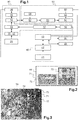
- Figure 1 schematically represents an apparatus combining an optical microscope, a photoluminescence or Raman spectrometer and a visualization device
- Figure 2 shows an example of a first image and a second image of a patterned sample displayed on a visualization device, and showing the borders of the area corresponding to the second image in overlay on the first image
- Figure 3 shows another example of a first image and a second image of another sample obtained using in addition an autofocus process
- Figs. 4A-4E show a few images from a stack of images acquired for a rutile sample using a 10X objective lens taken at different Z axial positions, and, respectively,
- Fig. 4F shows a reconstructed focused image based on a treatment of from a stack of images including images 4A-4E
- FIG. 4F shows a reconstructed focused image based on a treatment of from a stack of images including images 4A-4E
- a first aspect of the present disclosure concerns a new system and method for PL or Raman signal acquisition providing easy navigation on a sample surface.
- Figure 1 schematically shows a system combining an optical microscope 10, a photoluminescence or Raman spectrometry system 50, a processing system 40 and a display device 44.
- the optical microscope 10 comprises generally a microscope stand, at least one objective lens 11 and a sample holder for holding a sample to be analyzed.
- the objective lens 11 defines an optical axis OZ that is generally vertical.
- the optical microscope 10 comprises a low magnification objective 11 and a high magnification objective 12.
- the microscope 10 generally comprises motorized actuators 20 for moving the sample stage relatively to the objective lens 11 in three dimensions.
- the sample stage may be mounted on an XY scanning stage so as to translate the sample along X and/or Y directions and the microscope body is equipped with a Z stage enabling to move the microscope objective lens 11 along the OZ axis so as to adjust focusing.
- the sample stage may be mounted on an XYZ scanning stage enabling to move the sample in 3D.
- the sample stage may be mounted on a rotating stage.
- the optical microscope 10 includes an illumination turret comprising a beam splitter 13 used to direct the illumination light into objective, a switching mirror 14 used for coupling microscope with spectrometer and a tube lens 15 used to produce a sample image on CMOS camera. Further, the optical microscope 10 comprises a white light source 18 and an illumination condenser 17.
- the white light source 18 consists for example in a LED or halogen lamp.
- the white light source 18 generates a white light beam that is directed on the illumination condenser 17.
- the illumination condenser 17 forms an illumination light beam that is reflected on the beam splitter 13 toward the sample surface.
- the optical microscope 10 comprises a video camera 16 for acquisition of video images of the sample surface.
- the video images of the sample surface are formed using reflected light if the optical microscope 10 is configured to operate in reflection, or, respectively, using transmitted light if the optical microscope 10 is configured to operate in transmission.
- the PL or Raman spectrometry system 50 comprises a laser light source 51, a Rayleigh filter 52, coupling optics 54, a spectrometer 55 and a CCD camera 60.
- the laser light source 51 generates an excitation light beam at a determined wavelength.
- the Rayleigh filter 52 transmits the excitation light beam toward a switching mirror 14 in the beam path of the optical microscope so as to direct the excitation light beam toward the sample surface.
- the objective lens 11 focuses the excitation light beam on the sample.
- the switching mirror 14 enables to direct or not the excitation light beam toward the sample surface.
- the objective lens 11 collects a light beam that is back-scattered by the sample and returns the back-scattered light beam toward the switching mirror 14.
- the Rayleigh filter 52 separates Rayleigh scattered light, at the wavelength of the laser, from PL or Raman scattered light.
- the Rayleigh filter 52 comprises a notch type injection-rejection spectral filter.
- a confocal pinhole 53 is arranged so as to select Raman or PL light beam from a specific plane in the sample.
- the coupling optics 54 focus the PL or Raman scattered light on the entrance slit of the spectrometer 55.
- the CCD camera 60 is arranged at the output of the spectrometer 55 so as to detect PL or Raman spectra.
- the micro-spectrometry system comprises a processing system 40 including an acquisition unit 41, a treatment unit 42, a control unit or central processing unit 43 and a data storage unit 45.
- the acquisition unit 41 acquires images from the video camera 16 and/or, respectively, spectra from the CCD camera 60.
- the treatment unit 42 performs numerical processing on the acquired images and/or on spectra.
- the central processing unit 43 coordinates the operations of the scanning stage(s) 20, white light source 18, switching mirror 14, laser light source 51, Rayleigh filter 52, confocal pinhole 53, switching mirror 14 and spectrometer 55.
- the micro-spectrometry system comprises a display device 44 consisted of one screen or several screens.
- the display device 44 is connected to the central processing unit 43.
- the display device 44 displays in real time images of the sample acquired on the video camera 16 and/or spectra measured using the CCD camera 60 at a point of that sample.
- the microscope uses a first objective lens 11 having a low magnification of 4x, 5x or 10x.
- a motorized or piezo-actuated XY scanning stage 20 is used to drive displacement in X and/or Y directions during the sample's surface investigation or visualization.
- the microscope comprises a motorized Z stage or a piezo-actuated Z stage for relative displacement between the sample stage and the objective lens along OZ axis.
- the control unit 43 receives the current position of the XYZ stage in real time.
- the microscope camera 16 uses the first objective lens 11 of the microscope to detect a first image 71 of a sample surface obtained by reflection of the white light beam on the sample surface.
- the microscope camera and first objective lens are calibrated so as to determine a coordinate transfer function between the XY stage and the coordinates of array of pixels of the camera 16 combined with the first objective lens.
- each pixel of the first image 71 has determined positions in the XY coordinate system of the sample stage.
- the first image 71 is stored in a virtual image space allocated in the data storage unit 45. This first image 71 is used to initialize the content of a navigation map as illustrated on figure 2 .
- the first image 71 is stored in the data storage unit 45.
- the first image 71 is also displayed on the display device 44 as a static image.
- a second objective lens 12 replaces the first objective lens 11.
- the second objective lens 12 is a high magnification objective, for example 50x or 100x.
- the first objective lens 11 and the second objective lens 12 have the same optical axis (OZ).
- a calibration is used to determine an offset between the optical axis of the first objective lens 11 and the second objective lens 12.
- the processing unit 40 stores the magnification power corresponding to each objective lens, and possibly the offset.
- the microscope camera and second objective lens are calibrated so as to determine a coordinate transfer function between the XY stage and the coordinates of the array of pixels of the camera 16 combined with the second objective lens.
- a motorized Z stage or a piezo-actuated Z stage is used to adjust focus.
- the second objective lens 12 enables to zoom a particular region on the sample and to acquire a second image 72 of the same sample surface by reflection of the white light beam on the sample surface.
- Each pixel of the second image 72 has determined positions in the XY coordinate system of the sample stage.
- the CMOS video camera 16 records the zoomed region as a live video or as an image.
- This second image 72 (static or live) is displayed on the screen 44 as shown on figure 2 (right side). Due to the higher magnification, the second image 72 presents a narrow field of view that is, preferably at least partially, included in the field of view of the first image 71.
- the field of view on the camera 16 has generally a rectangular shape.
- the microscope system uses a single microscope objective lens to form the first image 71, which is a panoramic image, and the second image 72 with a small field of view.
- the first image 71 is obtained by acquiring a plurality of images taken at a plurality of X, Y positions and by panning this plurality of images as a function of their respective positions, so as to obtain a panoramic first image 71, providing a large field of view of the sample.
- a first image 71 is acquired with a large field of view and a second image 72 is acquired of the sample with a small field of view.
- the first image and the second image may be displayed on separate screens.
- the first and second images are displayed in separate windows on the same screen, for example using mosaic windows.
- the processing unit 40 calculates the position of a rectangular box corresponding to a field of view of the second image 72 in the coordinate system of the first image 71.
- An image 73 of the borders of this rectangular box is displayed in overlay on the first image 71 on the display device 44.
- the navigation map also includes the second image 72 that is displayed simultaneously next to the first image 71.
- the second image 72 provides a zoom on a narrow field of view, generally with higher spatial resolution and lower depth of field than the first image 71.
- the second image 72 is updated in real time as a function of the current position of the XY stage.
- the positions of the borders of the rectangular box 73 are also updated in real time as a function of current position of the XY stage.
- the processing unit 40 is also used to drive actuators for moving the sample stage relatively to the microscope objective. For example, the processing unit moves the sample stage in X and/or Y direction(s). In real time, the camera 16 records an updated second image 72. The processing unit calculates and updates also in real time the position of the rectangular box 73 on the display device 44.
- the user visualizes simultaneously the images 71, 72 and 73 and uses them for easy navigation on the sample surface, using any input device such as an integrated computer mouse, trackball, joystick, touchpad or touch screen.
- the user can easily use a "drag-and-move" function on the second image 72 (microscopic image).
- the XY stage moves in real time to display the real time second image at the desired XY position.
- the user can also click on or touch to select an area on the first image 71 in order to move the sample toward that area.
- the user easily controls the relative movement on the sample surface by viewing simultaneously the first image71, the second image 72 and the rectangular box 73.
- the user can easily select a region of interest on the sample and determine the direction of the movement.
- the rectangular box 73 is moveable to a target position using an appropriate user interface.
- the user interface comprises for example a computer mouse or a touchpad or a touch screen or any other interactive device.
- the control unit 43 detects the movement of the rectangular box 73 on the display device 44 and calculates the corresponding displacement of the XY stage.
- the control unit 43 drives the scanning stage 20 so that it applies a corresponding displacement to the XY scanning stage.
- an automatic displacement of the XY stage to a target position may be controlled by a user interface and visually on display device 44.
- the user can trigger a PL or Raman spectra acquisition in the selected ROI.
- the system provides a visually interactive navigation through the sample's map.
- This system and method offers a unique experience in terms of sample exploration and analysis. It makes the finding of a region of interest for Raman or PL measurement a lot easier.
- This system enables to navigate on a zoomed sample's surface and to visualize sample surface details.
- the sample shown on figure 2 has a generally flat surface and presents features having a high contrast.
- the sample's first image 71 obtained with a low magnification objective and a large field of view provides a navigation map having a coordinate system.
- the zoomed sample's second image 72 obtained with high magnification objective and containing sample's surface details is positioned in the coordinate system of the first image. This technique permits the user to have simultaneously global sample vision and sample' surface details vision in the region of interest.
- some samples may present a rough or textured surface and/or a surface topography having larger features than the depth of focus of the microscope objective lens.
- Such samples generally produce video images that are at least partially blurred.
- the first image 71 and/or second image 72 may be at least partially blurred due to being out-of-focus. Blurred images of the sample hinder easy navigation on the sample's surface, because detailed features are invisible. It is also more difficult to determine a ROI on the sample surface and to obtain precise Raman or PL microspectrometry data.
- a second aspect of the present disclosure concerns Z stage displacement combined with rapid images acquisition using the CMOS camera 16, so as to keep the field of view of the objective lens all time focused on sample's surface during navigation (see figure 3 ).
- This technology is called herein NavSharp standing for sharp navigation on a rough, textured sample surface or on a surface relief. This technology is combined with navigation map technique disclosed in the first aspect so as to provide sharp navigation on rough, textured or relief samples.
- the system uses a computer-controlled motorized or piezo XY stage.
- a motorized or piezo microscope Z stage is used for displacement along OZ axis.
- the control unit 43 moves the XY stage in user selected position.
- the video camera 16 acquires a sample image at current axial Z position.
- the control unit 43 moves Z stage on objective predetermined distance and camera 16 acquires another image.
- the treatment unit 42 proceeds with image analysis.
- the treatment algorithm is applied to the center area of image.
- image analysis means that it is applied to its center area, consisting of a few tens of pixels.
- the image treatment unit 42 evaluates image sharpness based on the combination of the mean square differences (MSD) of image pixel intensities in X and Y directions in the center area of each acquired image and for the corresponding axial Z position.
- MSD mean square differences
- I x,y represents the image intensity of pixel with ⁇ x,y ⁇ coordinates
- ⁇ represents the sum for all x and y coordinates inside the center area of M ⁇ N pixels
- d represents a lateral distance parameter
- a MSD for short distances (few pixels) and respectively a MSD for long distances (few tens pixels).
- the comparison of the MSD for short distances for the image at different axial Z positions permits to find the MSD maximum which defines the position of the best focus for image.
- the comparison of the MSDs for long distances for unfocused images at different Z permits to evaluate which of them is closer to the focus.
- the treatment unit 42 makes a decision on next Z movement based on both MSDs. If the current axial Z position is too far from focus, the value of the MSD for long distances doesn't permit to find direction to the focal plane. In this case, we are using the intensity of the reflected light acquired by camera 16.
- the treatment unit 42 calculates a mean image intensity at each axial Z position and its derivative with respect to Z.
- the control unit 43 moves the sample stage in the direction of a minimum of the derivative and in parallel the treatment unit 42 calculates the MSD for acquired image. Once the ratio of the MSD for newly acquired and previously acquired images is higher than a predefined threshold level, the treatment unit 42 switches to MSD method of focus finding.
- the position of derivative minimum is inside of a range of axial Z positions close to focus that corresponds to appearing of significant MSD variations. We confirmed this statement empirically in the experiments with different kind of samples.
- the treatment unit 42 analyses Z profiles composed of MSD and mean intensity of acquired images.
- the control unit 43 moves the Z stage to the axial Z position corresponding to the found MSD maximum and stores this Z focus position and the corresponding XY position.
- MSD profile has a maximum at lowest or, respectively, highest axial Z position in the measured range
- the control unit 43 moves the Z stage to another axial Z position below or, respectively, above the measured profile range.
- the image acquisition as a function of Z is resumed, and the MSD profile is updated. If the maximum is located inside the measured profile range than a new MSD profile maximum is searched with decreased Z displacements until Z focus position is found.
- the control unit 43 moves the Z stage to the new axial Z position corresponding to the found MSD maximum and stores this Z focus position and the corresponding XY position.
- the treatment unit 42 analyses the Z profile of mean intensity. This analysis requires measurements at least at three axial Z positions with large distances between them in order to evaluate the Z profile of mean intensity.
- the control unit 43 moves the Z stage to these axial Z positions and the camera 16 acquires the corresponding images.
- the treatment unit 42 determines the direction of the movement along OZ axis depending on the minimum of Z profile of mean intensity derivatives.
- the control unit 43 moves the sample stage in this direction and in parallel the treatment unit 42 calculates the MSDs for acquired images to find their maximum which determines the focus position.
- the Z stage is moved to the found focus position.
- the treatment unit 42 calculates MSD and mean image intensity and saves them together with current 3D (X,Y,Z) position in the data storage unit 45. Every time when user moves the stage to some X,Y position control unit 43 checks the stored values and select them if their X,Y values are shifted on less than a quarter size of the center area from actual position. In case if such selected values for different measurements are enough to define the focus position the control unit 43 moves the stage directly to determined position. Otherwise, the processing system 40 acquires the missing data to proceed with focus position finding.
- the proposed algorithm provides a smart live procedure for focus finding. When navigating on a region of interest that was already scanned previously, the best focus plane is directly selected.
- the processing system 40 acquires several images at different Z axial positions by moving rapidly the Z stage and using one or a combination of methods to detect each next potential target candidate : z value, select the sharpest plane and then move the stage so the user can see the sample at the best focus in an automatic manner.
- the sharp navigation method enables automatic focusing on the sample surface in the center area of the image by adjusting controllable Z axial position in real time.
- This automatic focus applies during XY stage movement and real time update of the acquired images.
- the user can select a ROI that is not in the center of the image, use the drag-and-move function to place the ROI in the center of the field of view of the camera so that the automatic focus be performed on the selected ROI.
- the Z profile of the derivative of the mean intensity of image in reflected light is used to determine the Z direction for focus position finding.
- the detection of an optimum focus Z axial position enables an easy navigation on the sample surface especially when using a confocal hole and/or when the sample has a rough, textured or relief surface.
- This method permits the user to find easily a region of interest (ROI) on a sample.
- This method also permits to visualize sample's surface details using an objective lens and camera with limited field of view and using a motorized or piezo XY stage.
- figure 3 shows a first image 71 of a mineral sample of gypsum in a right corner of a display device.
- the gypsum sample has a textured surface and a complex surface topography.
- Figure 3 also shows a second image 72 of a zoomed area on the same gypsum sample and the rectangular box 73 displayed in overlay on the first image showing the area corresponding to the field of view of the second image 72.
- Fig. 3 also shows the position of a pixel 56 at the center of the second image.
- the second image 72 shown here is focused in the center area. However, the second image 72 appears blurred at other X, Y positions outside of its center area.
- Fig. 3 demonstrates the efficiency of the sharp navigation technique for navigating on complex sample's surfaces.
- the user can define graphically an area 74 corresponding to a ROI for Raman or PL measurements.
- Example of figure 3 demonstrates that for a sample having a rough, irregular and rugged surface topography with Z variations larger than the depth of field of the objective lens 11, 12, the sample image is in focus only in the center area, but blurred in other parts, which hinders a navigation and a precise determination of the ROI as well as limits access to the sample surface for PL and/or Raman measurements.
- a third aspect of the present disclosure was developed and provides a method for visualizing a sample surface over the whole field of view.
- This third aspect is called view sharp standing for viewing sharply. It is used in combination with the sharp navigation and with the navigation map as detailed above.
- the system uses a computer-controlled motorized or piezo-actuated microscope Z stage for displacement along Z axis, in order to position the explored sample on desired height. It also uses the camera 16 for rapid image acquisition in high resolution.
- the user selects z scanning range from "short”, “standard”, “wide” and “maximal” range's options.
- the minimal, zmin, and maximal, zmax, values of these ranges as well as the scanning steps, ⁇ Z, are predefined in function of the selected objective and surface roughness.
- the control unit 43 scans the sample surface inside of the selected Z range with selected ⁇ Z step using motorized or piezo-actuated microscope Z stage. For each Z position, the video camera 16 acquires an image 131, 132, 133, 134, 135 of the same XY area of the sample. In other words, the relative XY position of the sample remains unchanged during the Z scans.
- the stack of acquired images at a plurality of axial Z positions below and above the reference or working plane corresponding to a focused center area are stored in the data storage unit 45.
- Each acquired image comprises focused and out of focus or blurred areas.
- the stack of these images contains the information about the all-in-focus sample surface inside of the field of view which could be extracted and presented in 2D image for the case when we do not take in account the information about pixel Z position or in 3D image for the case when pixel Z position information is used to recreate image topography.
- the stored pixel values in form of the stack of images could be represented in the column vector form for every X,Y position.
- the column vector corresponding to X,Y position or X,Y column vector consists of pixel intensity values for the same X,Y position at every Z position used for image acquisition.
- N the number pixels in acquired stack of images will be organized in N by M column vectors.
- the image treatment unit 42 applies pixel binning to every image in order to improve the sharpness detection.
- the pixel binned area for example 3 by 3 pixels or 5 by 5 pixels, is used to calculate the MSD value.
- the obtained MSD value is appropriated to correspondent X,Y column vector at correspondent Z position. In such way calculated column vectors represent the X,Y MSD Z profile.
- the MSD Z profile is analyzed for its first and second maxima and based on the confidence level criterion the found first maximum is selected or not.
- the treatment unit 42 calculates a confidence value for each found first maximum.
- the confidence levels (CL) equal to 2 (low), to 3 (medium) and to 4 (high) are introduced.
- the criterion for maximum selection is defined as follow. If the calculated CV is higher than CL, the treatment unit (42) selects the maximum value. Choosing a low confidence level may results in noise and false positive signal of MSD maximum value. In contrast, choosing a very high confidence level, may lead to a failure in detecting any MSD maximum value. In the case of textured, bright and homogeneously illuminated surface, the low or medium confidence level will be sufficient to find the sharpness maximum and reconstitute the sharp image of the all field of view. In the case of smoothed or badly illuminated surface the treatment unit 42 uses the high level of confidence and the CV may not be high enough to overcome CL. In this case an interpolation procedure is used to determine a MSD value using the found neighbor X,Y maximum MSD values for the same high confidence level.
- criterion for maximum sharpness selection is critical because it impacts the accuracy of sample surface determination. It also defines the time needed for the ViewSharp procedure execution. This criterion actually defines the computer's memory and processor resources to be used for efficient procedure execution.
- the treatment unit 42 applies a post-treatment to found values of MSD maximum describing a sharpness maximum. As an option, a smoothing is applied to remove artifact MSD values. For every found MSD maximum, the treatment unit 42 recovers the correspondent X,Y,Z coordinates and intensity value. The obtained coordinates could be used to present sample surface topography Z(X,Y). As control system 40 is using ⁇ Z step to scan sample surface, the recovered Z position values will be spaced by this step along Z axis forming the terraces on sample topography image. To approach the real surface, an interpolation step along OZ axis is applied based on analysis of the nearest neighbors' MSD values in OZ direction. Once the interpolation along Z axis is done, a continuous sample topography is obtained.
- the obtained sample surface topography image is reduced in X and Y directions due to pixel binning operation during sharpness calculation procedure.
- the treatment unit 42 applies another interpolation procedure along X and Y directions to restore all Z values corresponding to original pixel positions.
- the treatment unit 42 provides the all-in-focus surface topography image, wherein the new image has the same number of pixel as original image.
- obtained X,Y,Z values are used to build all-in-focus intensity 2D and 3D sample surface image wherein each new pixel intensity value corresponds to the intensity value of found maximum sharpness or interpolated intermediate intensity values.
- the obtained X,Y,Z and correspondent intensity values are stored by storage unit.
- the surface topography or Z map of the sample surface is stored in memory by unit 45 and is visualized by display unit 44.
- the all-in-focus 2D and 3D sample surface intensity images is stored in memory by unit 45 and is visualized by display unit 44.
- Figure 4F shows an example of such 2D reconstructed image 141.
- the reconstructed image 141 appears sharp over the whole field of view.
- This reconstructed image 141 may replace at least partially the first image 71 and/or replace the second image 72 displayed on the display device 44.
- the reconstructed image 141 enables easy navigation on a sample surface having a rough surface texture and/or an uneven surface topography.
- the reconstructed image 141 may also be used to update at least a part of the first image in the navigation map.
- the reconstructed image enables to visualize sample surface details and determine more precisely a ROI for Raman or PL measurements.
- Figure 5 shows an example of 2D all-in-focus surface intensity image of the another sample.
- the shown image corresponds to the field of view of the camera 16. We can see sharply all image surface. All blurred out of focus image zones were substituted by sharp in focus image zones.
- Figure 6 shows the reconstructed surface topography image for the same sample. The sample surface topography image gives a general sample view, permits to visualize the surface details and serve for general evaluation of method performance.
- Figure 7 shows another example of a 2D all-in-focus surface intensity image.
- Fig. 8 shows the corresponding 3D image surface intensity profile based on recovered surface focus Z positions. This image presents the particularity of the surface relief and enables to precisely select the ROI in 3D space.
- the selected ROI is used to acquire Raman or PL spectra at every selected pixel.
- Raman or PL spectrometry measurements are obtained with high lateral and axial resolution.
- Raman or PL spectra are acquired with the spectrometer 55 and the CCD camera 60.
- Raman or PL mapping is done by pixel by pixel scan of the ROI using found Z values for confocal acquisition of a spectrum from every pixel.
- the spectrum maximum or integral can be used as pixel value for image sharpening.
- the Raman response can be used for all-in focus image reconstruction using contrast value or intensity value instead of the white light reflection.
- Fig. 9 shows another example of sharpened image treated according to the above disclosure.
- the white light reflected intensity is used to generate 3D surface profile using ViewSharp method disclosed herein.
- Fig. 10 shows the corresponding Raman mapping measured point-by-point at the focused Z axial positions determined from the topography map. It is observed that the Raman spectral map has excellent spatial resolution.
- the comparison of figures 9 and 10 enables to analyze morphological features evidenced by the topography in view of Raman or PL measurements which give additional information about chemical composition.
Description
- The invention relates to a method and system for visualizing and mapping the surface of a sample in two-dimensions (2D) or three-dimensions (3D) over a broad spatial range, for example from millimetric scale to micron scale, and with high lateral and axial resolutions in order to perform microspectrometry measurements in a precisely selected region of interest (ROI).
- The invention also concerns a method and system for easy navigation on a sample surface with high precision and over a broad spatial range, for example from millimetric to micron scale, in order to select a region of interest (ROI) for performing spectrometric analysis or spectroscopic imaging, such as for example photoluminescence (PL) or Raman imaging.
- Recent two decades have seen drastic progress in PL and Raman spectrometer developments due to huge advances in photon detectors and light source developments. Photon detection systems include in particular CCD, EMCCD and CMOS cameras and new generations of avalanche photodiodes and photomultipliers with improved characteristics. New light sources include compact solid state lasers covering spectral range from UV light to near infrared light with average power of tens of mW, well enough to produce PL or Raman signal.
- An important breakthrough in PL and Raman techniques development resulted from the combination of spectroscopy and microscopy techniques. Despite the fact that both techniques are very old, recent developments in electronics and photonics have enabled important innovations.
- In particular, modern microscope spectrometers comprise autofocus systems to find and follow the sample surface. The principals of functioning of autofocus systems have optical or numerical origins.
- The optical hardware autofocus systems use a laser to measure the distance to sample surface or white light interference to keep the distance to the surface constant. They can also use the intensity of the light reflected from the sample surface or intensity of the sample spectral response to identify the sample surface location through the maximum of the measured signal. In general all optical hardware autofocus systems are point by point measurement methods and demand a time to collect the information from an area of N by N pixels. In function of time spent on one pixel and of number of pixels the total time can vary from minutes to several hours. Another disadvantage of optical autofocus methods is their sensibility to the nature of the sample surface. In case of strongly diffusive, semitransparent, inclined, or relief surface the method will provide incorrect results or even will not work at all. Moreover, the price of the optical hardware autofocus device increases the total cost of microscope spectrometer.
- The alternative to use of optical hardware autofocus systems is the use of digital or numerical autofocus systems. These systems don't bring any additional cost into device as they are using already present video image hardware as optical objective lenses, light transmission optics and detection devices as CMOS or CCD cameras. Only investment is development of mathematical algorithm integrated into software to find and keep the focus on studied or measured samples. Such systems are already developed and found common use in the digital photo cameras, smart phones or digital microscopy. In every particular realization the inventors proposed their particular solution of hardware and software realizations and the applications differ from device to device. The important advantage of the digital autofocus is a large working area corresponding to a field of view. Digital autofocus proceed with millions pixels measurements simultaneously. Digital autofocus systems are generally based on image contrast or sharpness analysis. Their software comprises an algorithm that analyses the images contrast or sharpness as a function of z coordinates and determines the best focus position. The correspondence of the high contrast or sharp image to sample location in focus made possible this software approach.
- For rather flat, smooth samples, autofocus permits to sharply visualize the whole field of view. However, most samples present a rough surface with significant variation along OZ axis which requires running the optical autofocus at each point of ROI for sample surface visualization and for PL or and/or Raman surface imaging. As mentioned above, this is a major drawback of optical hardware autofocus systems for the reason that it is highly time consuming. Moreover, it is difficult for a user to select a region of interest (ROI) for performing PL or Raman measurements of a sample because a part of sample surface inside of the field of view of a microscope objective would be blurred. Thus, it is difficult to ascertain the ROI area during use thereof.
- A Raman microscope with selectable ROI is disclosed in
DE 10 2012 021 726 A1 .US 5,790,710 discloses the determination of focus position from a z-stack. The creation of a 3D topography map from a z-stack is disclosed in "Highly accurate non-contact characterization of engineering surfaces using confocal microscopy", H-J Jordan, M Wegner and H Tiziani, Measurement Science and Technology, Volume 9, Number 7, 1142-1151. - Therefore, in order to remedy the drawbacks of the prior art, one object of the invention is to provide an optical micro-spectrometry system comprising the features of claim 1.
- A further object of the invention is to provide a micro-spectrometry measurement method comprising the steps of claim 6.
- This system and method enable Raman signal acquisition in a selected region of interest (ROI) while providing fast and easy navigation on sample's surface.
- Preferably, the region of interest for Raman or PL measurements is selected among: a rectangular area, a disk-shaped area, a user designated area, a line, a set of randomly selected points and a set of user designated points.
- This method and system are fast and require no additional hardware component.
- Favourable modifications of the system of claim 1 and the method of claim 6 are defined in the respective dependent claims.
- The invention will be better understood when referring to the appended drawings wherein:
Figure 1 schematically represents an apparatus combining an optical microscope, a photoluminescence or Raman spectrometer and a visualization device;Figure 2 shows an example of a first image and a second image of a patterned sample displayed on a visualization device, and showing the borders of the area corresponding to the second image in overlay on the first image;Figure 3 shows another example of a first image and a second image of another sample obtained using in addition an autofocus process;Figs. 4A-4E show a few images from a stack of images acquired for a rutile sample using a 10X objective lens taken at different Z axial positions, and, respectively,Fig. 4F shows a reconstructed focused image based on a treatment
of from a stack of images including images 4A-4E; -
Figure 5 shows a virtually sharpened image of an aspirin tablet sample in 2D obtained with 10X objective andfig. 6 shows the corresponding surface topography map; -
Fig. 7 shows a reconstructed 2D focused image of a gypsum sample using a 100X objective lens andfig. 8 shows the corresponding all-in-focus 3D reconstructed surface topography; -
Fig. 9 shows a 2D surface topography image of a rutile sample at 100x andfig. 10 shows the corresponding Raman spectrometry image. - Herein is disclosed a new digital approach for automatic focus finding for sample surface during sample movement or sample surface navigation, simultaneous visualization of whole sample surface inside of field of view, registering of this omnifocal sample surface inside of the field of view for further combination in mosaic image and easy navigation on large sample image with zoom on its details for the purpose to select a precise and sophisticate ROI for further PL and Raman measurements and sample surface imaging.
- A first aspect of the present disclosure concerns a new system and method for PL or Raman signal acquisition providing easy navigation on a sample surface.
-
Figure 1 schematically shows a system combining anoptical microscope 10, a photoluminescence orRaman spectrometry system 50, aprocessing system 40 and adisplay device 44. - The
optical microscope 10 comprises generally a microscope stand, at least oneobjective lens 11 and a sample holder for holding a sample to be analyzed. Theobjective lens 11 defines an optical axis OZ that is generally vertical. Preferably, theoptical microscope 10 comprises alow magnification objective 11 and ahigh magnification objective 12. - The
microscope 10 generally comprisesmotorized actuators 20 for moving the sample stage relatively to theobjective lens 11 in three dimensions. For example, the sample stage may be mounted on an XY scanning stage so as to translate the sample along X and/or Y directions and the microscope body is equipped with a Z stage enabling to move the microscopeobjective lens 11 along the OZ axis so as to adjust focusing. Alternatively, the sample stage may be mounted on an XYZ scanning stage enabling to move the sample in 3D. Alternatively or complementarily, the sample stage may be mounted on a rotating stage. - Within the present document, we consider an XYZ orthonormal coordinate system wherein the OZ axis corresponds to the optical axis of the microscope, and wherein the OX axis and OY axis are transverse to the OZ axis. Generally, the OZ axis is vertical.
- The
optical microscope 10 includes an illumination turret comprising abeam splitter 13 used to direct the illumination light into objective, a switchingmirror 14 used for coupling microscope with spectrometer and atube lens 15 used to produce a sample image on CMOS camera. Further, theoptical microscope 10 comprises awhite light source 18 and anillumination condenser 17. Thewhite light source 18 consists for example in a LED or halogen lamp. Thewhite light source 18 generates a white light beam that is directed on theillumination condenser 17. Theillumination condenser 17 forms an illumination light beam that is reflected on thebeam splitter 13 toward the sample surface. - In addition, the
optical microscope 10 comprises avideo camera 16 for acquisition of video images of the sample surface. The video images of the sample surface are formed using reflected light if theoptical microscope 10 is configured to operate in reflection, or, respectively, using transmitted light if theoptical microscope 10 is configured to operate in transmission. - The PL or
Raman spectrometry system 50 comprises alaser light source 51, aRayleigh filter 52,coupling optics 54, aspectrometer 55 and aCCD camera 60. Thelaser light source 51 generates an excitation light beam at a determined wavelength. On the input path, theRayleigh filter 52 transmits the excitation light beam toward a switchingmirror 14 in the beam path of the optical microscope so as to direct the excitation light beam toward the sample surface. Theobjective lens 11 focuses the excitation light beam on the sample. The switchingmirror 14 enables to direct or not the excitation light beam toward the sample surface. Theobjective lens 11 collects a light beam that is back-scattered by the sample and returns the back-scattered light beam toward the switchingmirror 14. On the return path, theRayleigh filter 52 separates Rayleigh scattered light, at the wavelength of the laser, from PL or Raman scattered light. For example theRayleigh filter 52 comprises a notch type injection-rejection spectral filter. Optionally, aconfocal pinhole 53 is arranged so as to select Raman or PL light beam from a specific plane in the sample. Thecoupling optics 54 focus the PL or Raman scattered light on the entrance slit of thespectrometer 55. TheCCD camera 60 is arranged at the output of thespectrometer 55 so as to detect PL or Raman spectra. - Generally, the micro-spectrometry system comprises a
processing system 40 including anacquisition unit 41, atreatment unit 42, a control unit orcentral processing unit 43 and adata storage unit 45. Theacquisition unit 41 acquires images from thevideo camera 16 and/or, respectively, spectra from theCCD camera 60. Thetreatment unit 42 performs numerical processing on the acquired images and/or on spectra. Thecentral processing unit 43 coordinates the operations of the scanning stage(s) 20,white light source 18, switchingmirror 14,laser light source 51,Rayleigh filter 52,confocal pinhole 53, switchingmirror 14 andspectrometer 55. - Finally, the micro-spectrometry system comprises a
display device 44 consisted of one screen or several screens. Thedisplay device 44 is connected to thecentral processing unit 43. For example, thedisplay device 44 displays in real time images of the sample acquired on thevideo camera 16 and/or spectra measured using theCCD camera 60 at a point of that sample. - We will now describe the configuration and operation of such a microspectrometry system according to a first aspect of the present disclosure that provides a navigation map at the sample scale for selecting a ROI and performing Raman or PL spectrometry measurements in that ROI.
- For example, the microscope uses a first
objective lens 11 having a low magnification of 4x, 5x or 10x. - A motorized or piezo-actuated
XY scanning stage 20 is used to drive displacement in X and/or Y directions during the sample's surface investigation or visualization. Preferably, the microscope comprises a motorized Z stage or a piezo-actuated Z stage for relative displacement between the sample stage and the objective lens along OZ axis. Thecontrol unit 43 receives the current position of the XYZ stage in real time. - Using the first
objective lens 11 of the microscope, themicroscope camera 16 detects afirst image 71 of a sample surface obtained by reflection of the white light beam on the sample surface. The microscope camera and first objective lens are calibrated so as to determine a coordinate transfer function between the XY stage and the coordinates of array of pixels of thecamera 16 combined with the first objective lens. Thus, each pixel of thefirst image 71 has determined positions in the XY coordinate system of the sample stage. Thefirst image 71 is stored in a virtual image space allocated in thedata storage unit 45. Thisfirst image 71 is used to initialize the content of a navigation map as illustrated onfigure 2 . Thefirst image 71 is stored in thedata storage unit 45. Thefirst image 71 is also displayed on thedisplay device 44 as a static image. - Then, a second
objective lens 12 replaces the firstobjective lens 11. The secondobjective lens 12 is a high magnification objective, for example 50x or 100x. Preferably the firstobjective lens 11 and the secondobjective lens 12 have the same optical axis (OZ). Alternatively, a calibration is used to determine an offset between the optical axis of the firstobjective lens 11 and the secondobjective lens 12. Theprocessing unit 40 stores the magnification power corresponding to each objective lens, and possibly the offset. Similarly as with the first objective lens, the microscope camera and second objective lens are calibrated so as to determine a coordinate transfer function between the XY stage and the coordinates of the array of pixels of thecamera 16 combined with the second objective lens. Optionally, a motorized Z stage or a piezo-actuated Z stage is used to adjust focus. - The second
objective lens 12 enables to zoom a particular region on the sample and to acquire asecond image 72 of the same sample surface by reflection of the white light beam on the sample surface. Each pixel of thesecond image 72 has determined positions in the XY coordinate system of the sample stage. TheCMOS video camera 16 records the zoomed region as a live video or as an image. This second image 72 (static or live) is displayed on thescreen 44 as shown onfigure 2 (right side). Due to the higher magnification, thesecond image 72 presents a narrow field of view that is, preferably at least partially, included in the field of view of thefirst image 71. The field of view on thecamera 16 has generally a rectangular shape. - Alternatively, the microscope system uses a single microscope objective lens to form the
first image 71, which is a panoramic image, and thesecond image 72 with a small field of view. In this case, thefirst image 71 is obtained by acquiring a plurality of images taken at a plurality of X, Y positions and by panning this plurality of images as a function of their respective positions, so as to obtain a panoramicfirst image 71, providing a large field of view of the sample. - In all cases, a
first image 71 is acquired with a large field of view and asecond image 72 is acquired of the sample with a small field of view. The first image and the second image may be displayed on separate screens. Alternatively, the first and second images are displayed in separate windows on the same screen, for example using mosaic windows. - Moreover, the
processing unit 40 calculates the position of a rectangular box corresponding to a field of view of thesecond image 72 in the coordinate system of thefirst image 71. Animage 73 of the borders of this rectangular box is displayed in overlay on thefirst image 71 on thedisplay device 44. Thus, we obtain a navigation map comprising thefirst image 71 and therectangular box 73 displayed in overlay. The navigation map also includes thesecond image 72 that is displayed simultaneously next to thefirst image 71. Thesecond image 72 provides a zoom on a narrow field of view, generally with higher spatial resolution and lower depth of field than thefirst image 71. Thesecond image 72 is updated in real time as a function of the current position of the XY stage. Concurrently, the positions of the borders of therectangular box 73 are also updated in real time as a function of current position of the XY stage. - The
processing unit 40 is also used to drive actuators for moving the sample stage relatively to the microscope objective. For example, the processing unit moves the sample stage in X and/or Y direction(s). In real time, thecamera 16 records an updatedsecond image 72. The processing unit calculates and updates also in real time the position of therectangular box 73 on thedisplay device 44. - The user visualizes simultaneously the
images first image 71 in order to move the sample toward that area. - Thus, the user easily controls the relative movement on the sample surface by viewing simultaneously the first image71, the
second image 72 and therectangular box 73. - The user can easily select a region of interest on the sample and determine the direction of the movement.
- Alternatively and/or complementarily, the
rectangular box 73 is moveable to a target position using an appropriate user interface. The user interface comprises for example a computer mouse or a touchpad or a touch screen or any other interactive device. Thecontrol unit 43 detects the movement of therectangular box 73 on thedisplay device 44 and calculates the corresponding displacement of the XY stage. Thecontrol unit 43 drives thescanning stage 20 so that it applies a corresponding displacement to the XY scanning stage. Thus, an automatic displacement of the XY stage to a target position may be controlled by a user interface and visually ondisplay device 44. - When the XY stage has moved to the desired ROI, the user can trigger a PL or Raman spectra acquisition in the selected ROI.
- Thus, the system provides a visually interactive navigation through the sample's map. This system and method offers a unique experience in terms of sample exploration and analysis. It makes the finding of a region of interest for Raman or PL measurement a lot easier.
- This system enables to navigate on a zoomed sample's surface and to visualize sample surface details. The sample shown on
figure 2 has a generally flat surface and presents features having a high contrast. - Thus, the sample's
first image 71 obtained with a low magnification objective and a large field of view provides a navigation map having a coordinate system. At the same time, the zoomed sample'ssecond image 72 obtained with high magnification objective and containing sample's surface details is positioned in the coordinate system of the first image. This technique permits the user to have simultaneously global sample vision and sample' surface details vision in the region of interest. - However, some samples may present a rough or textured surface and/or a surface topography having larger features than the depth of focus of the microscope objective lens. Such samples generally produce video images that are at least partially blurred. Also, using a confocal system, the
first image 71 and/orsecond image 72 may be at least partially blurred due to being out-of-focus. Blurred images of the sample hinder easy navigation on the sample's surface, because detailed features are invisible. It is also more difficult to determine a ROI on the sample surface and to obtain precise Raman or PL microspectrometry data. - A second aspect of the present disclosure concerns Z stage displacement combined with rapid images acquisition using the
CMOS camera 16, so as to keep the field of view of the objective lens all time focused on sample's surface during navigation (seefigure 3 ). - This technology is called herein NavSharp standing for sharp navigation on a rough, textured sample surface or on a surface relief. This technology is combined with navigation map technique disclosed in the first aspect so as to provide sharp navigation on rough, textured or relief samples.
- The system uses a computer-controlled motorized or piezo XY stage. A motorized or piezo microscope Z stage is used for displacement along OZ axis. The
control unit 43 moves the XY stage in user selected position. Thevideo camera 16 acquires a sample image at current axial Z position. Thecontrol unit 43 moves Z stage on objective predetermined distance andcamera 16 acquires another image. For each acquired image, thetreatment unit 42 proceeds with image analysis. The treatment algorithm is applied to the center area of image. In the following description of the second aspect (NavSharp description), the term image analysis means that it is applied to its center area, consisting of a few tens of pixels. - Here, the
image treatment unit 42 evaluates image sharpness based on the combination of the mean square differences (MSD) of image pixel intensities in X and Y directions in the center area of each acquired image and for the corresponding axial Z position. - Within the present disclosure, MSD is defined as follows:

- Where Ix,y represents the image intensity of pixel with {x,y} coordinates, ∑ represents the sum for all x and y coordinates inside the center area of M ∗ N pixels, and d represents a lateral distance parameter.
- In details, to evaluate an image sharpness at different axial Z positions, we calculate a MSD for short distances (few pixels) and respectively a MSD for long distances (few tens pixels). The comparison of the MSD for short distances for the image at different axial Z positions permits to find the MSD maximum which defines the position of the best focus for image. The comparison of the MSDs for long distances for unfocused images at different Z permits to evaluate which of them is closer to the focus. The
treatment unit 42 makes a decision on next Z movement based on both MSDs. If the current axial Z position is too far from focus, the value of the MSD for long distances doesn't permit to find direction to the focal plane. In this case, we are using the intensity of the reflected light acquired bycamera 16. Thetreatment unit 42 calculates a mean image intensity at each axial Z position and its derivative with respect to Z. Thecontrol unit 43 moves the sample stage in the direction of a minimum of the derivative and in parallel thetreatment unit 42 calculates the MSD for acquired image. Once the ratio of the MSD for newly acquired and previously acquired images is higher than a predefined threshold level, thetreatment unit 42 switches to MSD method of focus finding. In the present disclosure, we state that the position of derivative minimum is inside of a range of axial Z positions close to focus that corresponds to appearing of significant MSD variations. We confirmed this statement empirically in the experiments with different kind of samples. - Two or more images at different axial Z positions and nearly the same (shifted less then a quarter of the analyzed area) XY positions are needed to make a decision on the next movement. The
treatment unit 42 analyses Z profiles composed of MSD and mean intensity of acquired images. - If the Z profile of MSD clearly indicates the position of a maximum inside the profile zone, the
control unit 43 moves the Z stage to the axial Z position corresponding to the found MSD maximum and stores this Z focus position and the corresponding XY position. In another case, if MSD profile has a maximum at lowest or, respectively, highest axial Z position in the measured range, then thecontrol unit 43 moves the Z stage to another axial Z position below or, respectively, above the measured profile range. The image acquisition as a function of Z is resumed, and the MSD profile is updated. If the maximum is located inside the measured profile range than a new MSD profile maximum is searched with decreased Z displacements until Z focus position is found. Thecontrol unit 43 moves the Z stage to the new axial Z position corresponding to the found MSD maximum and stores this Z focus position and the corresponding XY position. - If the MSD profile is nearly flat, the Z movement direction cannot be found. In this case, the
treatment unit 42 analyses the Z profile of mean intensity. This analysis requires measurements at least at three axial Z positions with large distances between them in order to evaluate the Z profile of mean intensity. Thecontrol unit 43 moves the Z stage to these axial Z positions and thecamera 16 acquires the corresponding images. Thetreatment unit 42 determines the direction of the movement along OZ axis depending on the minimum of Z profile of mean intensity derivatives. Thecontrol unit 43 moves the sample stage in this direction and in parallel thetreatment unit 42 calculates the MSDs for acquired images to find their maximum which determines the focus position. The Z stage is moved to the found focus position. - For every acquired image, the
treatment unit 42 calculates MSD and mean image intensity and saves them together with current 3D (X,Y,Z) position in thedata storage unit 45. Every time when user moves the stage to some X,Yposition control unit 43 checks the stored values and select them if their X,Y values are shifted on less than a quarter size of the center area from actual position. In case if such selected values for different measurements are enough to define the focus position thecontrol unit 43 moves the stage directly to determined position. Otherwise, theprocessing system 40 acquires the missing data to proceed with focus position finding. The proposed algorithm provides a smart live procedure for focus finding. When navigating on a region of interest that was already scanned previously, the best focus plane is directly selected. - Thus, the
processing system 40 acquires several images at different Z axial positions by moving rapidly the Z stage and using one or a combination of methods to detect each next potential target candidate : z value, select the sharpest plane and then move the stage so the user can see the sample at the best focus in an automatic manner. - Thus, the sharp navigation method enables automatic focusing on the sample surface in the center area of the image by adjusting controllable Z axial position in real time. This automatic focus applies during XY stage movement and real time update of the acquired images. Also, the user can select a ROI that is not in the center of the image, use the drag-and-move function to place the ROI in the center of the field of view of the camera so that the automatic focus be performed on the selected ROI.
- Moreover, in order to speed up the selection of the focus plane and also to facilitate its finding, the Z profile of the derivative of the mean intensity of image in reflected light is used to determine the Z direction for focus position finding.
- The detection of an optimum focus Z axial position enables an easy navigation on the sample surface especially when using a confocal hole and/or when the sample has a rough, textured or relief surface.
- This method permits the user to find easily a region of interest (ROI) on a sample. This method also permits to visualize sample's surface details using an objective lens and camera with limited field of view and using a motorized or piezo XY stage.
- As an example,
figure 3 shows afirst image 71 of a mineral sample of gypsum in a right corner of a display device. The gypsum sample has a textured surface and a complex surface topography.Figure 3 also shows asecond image 72 of a zoomed area on the same gypsum sample and therectangular box 73 displayed in overlay on the first image showing the area corresponding to the field of view of thesecond image 72.Fig. 3 also shows the position of apixel 56 at the center of the second image. Thesecond image 72 shown here is focused in the center area. However, thesecond image 72 appears blurred at other X, Y positions outside of its center area.Fig. 3 demonstrates the efficiency of the sharp navigation technique for navigating on complex sample's surfaces. - On the
second image 72, the user can define graphically anarea 74 corresponding to a ROI for Raman or PL measurements. - Example of
figure 3 demonstrates that for a sample having a rough, irregular and rugged surface topography with Z variations larger than the depth of field of theobjective lens - Thus, a third aspect of the present disclosure was developed and provides a method for visualizing a sample surface over the whole field of view.
- This third aspect is called view sharp standing for viewing sharply. It is used in combination with the sharp navigation and with the navigation map as detailed above.
- The system uses a computer-controlled motorized or piezo-actuated microscope Z stage for displacement along Z axis, in order to position the explored sample on desired height. It also uses the
camera 16 for rapid image acquisition in high resolution. We select one of theobjectives - The
control unit 43 scans the sample surface inside of the selected Z range with selected ΔZ step using motorized or piezo-actuated microscope Z stage. For each Z position, thevideo camera 16 acquires animage Fig. 4A shows for example animage 131 of a sample area taken in a Z=140 µm plane.Fig. 4B shows anotherimage 132 of the same sample area taken in a Z=70 µm plane.Fig. 4C shows anotherimage 133 of the same sample area taken in a Z=0 µm reference plane.Fig. 4D shows anotherimage 134 of the same sample area taken in a Z=-70 µm plane. And,Fig. 4E shows anotherimage 135 of the same sample area taken in a Z=-140 µm plane. - The stack of acquired images at a plurality of axial Z positions below and above the reference or working plane corresponding to a focused center area are stored in the
data storage unit 45. Each acquired image comprises focused and out of focus or blurred areas. The stack of these images contains the information about the all-in-focus sample surface inside of the field of view which could be extracted and presented in 2D image for the case when we do not take in account the information about pixel Z position or in 3D image for the case when pixel Z position information is used to recreate image topography. The stored pixel values in form of the stack of images could be represented in the column vector form for every X,Y position. The column vector corresponding to X,Y position or X,Y column vector consists of pixel intensity values for the same X,Y position at every Z position used for image acquisition. In case of field of view characterized by N by M pixels the all pixels in acquired stack of images will be organized in N by M column vectors. - The
image treatment unit 42 analyses every acquired image. Thus, the acquisition of the stack of sample's images is followed by their treatment in real time. Each acquired image is optionally treated to remove the noise and artifact and then it is sharpened by applying Laplacian operator in Z direction. Each pixel value I(z) is substituted with l(z)+dl(z), where dl(z) is a local differential calculated on pixel binned area. More precisely, dl(z) is calculated in next way dI(z)=(I(z)∗2-I(z-1)-I(z+1))∗coefficient, where the coefficient corresponds to different level of sharpening. This operation amplifies the observed sharpness to facilitate the maximum sharpness finding. Depending on the mathematical expression of Laplacian operator, it is possible to sharpen the acquired image presented by a matrix of intensity values, I (X, Y, Z), to different levels. It is possible to use the sharpened pixel value in a final ViewSharp image reconstruction. - The
image treatment unit 42 applies pixel binning to every image in order to improve the sharpness detection. The pixel binned area, for example 3 by 3 pixels or 5 by 5 pixels, is used to calculate the MSD value. The obtained MSD value is appropriated to correspondent X,Y column vector at correspondent Z position. In such way calculated column vectors represent the X,Y MSD Z profile. The MSD Z profile is analyzed for its first and second maxima and based on the confidence level criterion the found first maximum is selected or not. Thetreatment unit 42 calculates a confidence value for each found first maximum. A confidence value, named here CV, is defined by the ratio of the first MSD maximum to the sum of the second MSD maximum and mean MSD value:
- Based on empirical data the confidence levels (CL) equal to 2 (low), to 3 (medium) and to 4 (high) are introduced. The criterion for maximum selection is defined as follow. If the calculated CV is higher than CL, the treatment unit (42) selects the maximum value. Choosing a low confidence level may results in noise and false positive signal of MSD maximum value. In contrast, choosing a very high confidence level, may lead to a failure in detecting any MSD maximum value. In the case of textured, bright and homogeneously illuminated surface, the low or medium confidence level will be sufficient to find the sharpness maximum and reconstitute the sharp image of the all field of view. In the case of smoothed or badly illuminated surface the
treatment unit 42 uses the high level of confidence and the CV may not be high enough to overcome CL. In this case an interpolation procedure is used to determine a MSD value using the found neighbor X,Y maximum MSD values for the same high confidence level. - The definition of criterion for maximum sharpness selection is critical because it impacts the accuracy of sample surface determination. It also defines the time needed for the ViewSharp procedure execution. This criterion actually defines the computer's memory and processor resources to be used for efficient procedure execution.
- The
treatment unit 42 applies a post-treatment to found values of MSD maximum describing a sharpness maximum. As an option, a smoothing is applied to remove artifact MSD values. For every found MSD maximum, thetreatment unit 42 recovers the correspondent X,Y,Z coordinates and intensity value. The obtained coordinates could be used to present sample surface topography Z(X,Y). Ascontrol system 40 is using ΔZ step to scan sample surface, the recovered Z position values will be spaced by this step along Z axis forming the terraces on sample topography image. To approach the real surface, an interpolation step along OZ axis is applied based on analysis of the nearest neighbors' MSD values in OZ direction. Once the interpolation along Z axis is done, a continuous sample topography is obtained. The obtained sample surface topography image is reduced in X and Y directions due to pixel binning operation during sharpness calculation procedure. To restore the obtained sample topography image to the original size with high spatial resolution, thetreatment unit 42 applies another interpolation procedure along X and Y directions to restore all Z values corresponding to original pixel positions. Thetreatment unit 42 provides the all-in-focus surface topography image, wherein the new image has the same number of pixel as original image. Thus obtained X,Y,Z values are used to build all-in-focus intensity 2D and 3D sample surface image wherein each new pixel intensity value corresponds to the intensity value of found maximum sharpness or interpolated intermediate intensity values. - The obtained X,Y,Z and correspondent intensity values are stored by storage unit. The surface topography or Z map of the sample surface is stored in memory by
unit 45 and is visualized bydisplay unit 44. The all-in-focus 2D and 3D sample surface intensity images is stored in memory byunit 45 and is visualized bydisplay unit 44.Figure 4F shows an example of such 2D reconstructedimage 141. Thereconstructed image 141 appears sharp over the whole field of view. Thisreconstructed image 141 may replace at least partially thefirst image 71 and/or replace thesecond image 72 displayed on thedisplay device 44. Thereconstructed image 141 enables easy navigation on a sample surface having a rough surface texture and/or an uneven surface topography. Thereconstructed image 141 may also be used to update at least a part of the first image in the navigation map. Thus, the reconstructed image enables to visualize sample surface details and determine more precisely a ROI for Raman or PL measurements. -
Figure 5 shows an example of 2D all-in-focus surface intensity image of the another sample. The shown image corresponds to the field of view of thecamera 16. We can see sharply all image surface. All blurred out of focus image zones were substituted by sharp in focus image zones.Figure 6 shows the reconstructed surface topography image for the same sample. The sample surface topography image gives a general sample view, permits to visualize the surface details and serve for general evaluation of method performance. -
Figure 7 shows another example of a 2D all-in-focus surface intensity image. We can see very sharp image of sample surface where Z variations is many times of the objective field of view.Fig. 8 shows the corresponding 3D image surface intensity profile based on recovered surface focus Z positions. This image presents the particularity of the surface relief and enables to precisely select the ROI in 3D space. The selected ROI is used to acquire Raman or PL spectra at every selected pixel. Thus, Raman or PL spectrometry measurements are obtained with high lateral and axial resolution. Raman or PL spectra are acquired with thespectrometer 55 and theCCD camera 60. - Raman or PL mapping is done by pixel by pixel scan of the ROI using found Z values for confocal acquisition of a spectrum from every pixel. Alternatively, the spectrum maximum or integral can be used as pixel value for image sharpening. Indeed, in a case where the excitation laser light does not penetrate into the sample, the Raman response can be used for all-in focus image reconstruction using contrast value or intensity value instead of the white light reflection.
-
Fig. 9 shows another example of sharpened image treated according to the above disclosure. The white light reflected intensity is used to generate 3D surface profile using ViewSharp method disclosed herein.Fig. 10 shows the corresponding Raman mapping measured point-by-point at the focused Z axial positions determined from the topography map. It is observed that the Raman spectral map has excellent spatial resolution. The comparison offigures 9 and 10 enables to analyze morphological features evidenced by the topography in view of Raman or PL measurements which give additional information about chemical composition.
Claims (11)
- An optical micro-spectrometry system comprising:- an optical microscope (10) comprising a sample holder for holding a sample to be analyzed and at least one microscope objective (11, 12) defining an optical axis (OZ) ;- a spectrometry system (50) comprising a light source (51) adapted for generating an excitation light beam, a spectrometer (55) and a detection system (60),- an optical system (14) adapted to direct the excitation light beam on the sample through said at least one microscope objective (11, 12) and to collect a Raman or photoluminescence light beam generated by scattering of the excitation light beam on the sample, the optical system (14) being adapted to direct said Raman or photoluminescence light beam toward said spectrometer (55) and said detection system (60) ;
and- an actuating system (20) for driving a relative lateral (dX, dY) and axial (dZ) movement between the sample holder and said at least one microscope objective (11, 12),characterized in that the optical micro-spectrometry system comprises:- another light source (18) for generating an illumination beam ;- an imaging system (16, 41) arranged in combination with said at least one microscope objective (11, 12) and configured for acquiring a plurality of images formed by reflection or transmission of the illumination beam from a sample surface at a plurality of axial positions (Z) along the optical axis (OZ) ;- a processing system (40) configured to sharpen said plurality of images by substituting each pixel value I(z) with I(z)+dI(z), where dl(z) is calculated by dI(z)=(I(z)∗2-I(z-1)-I(z+1))∗coefficient, where the coefficient corresponds to a level of sharpening;- the processing system (40) is configured to determine a plurality of column vectors of pixels (Px, Py) for said plurality of sharpened images of the sample as a function of said plurality of axial positions (Z) along the optical axis (OZ) ;- the processing system (40) being configured to evaluate a sharpness profile or a contrast profile, using a mean square difference or variations of a gradient or of a first derivative profile or, respectively, a second derivative profile for each of the plurality of column vectors of pixels (Px, Py) and an associated confidence level value ;- the processing system (40) being configured to analyze said sharpness or contrast profile, for each of said column vector of pixels (Px, Py) with the associated confidence level value and to deduce therefrom a focus position for each of the plurality of column vector of pixels (Px, Py) ; and- the processing system (40) being configured to determine three-dimensional coordinates of the focus position and corresponding pixel intensity for each of the plurality of column vector of pixels (Px, Py) and to build a sample topography image representing the sample surface in three-dimensions and/or in two-dimensions,- a display system (44) configured for displaying the sample topography image;- a user interface configured for selecting a region of interest in the sample topography image;- the actuating system (20) being configured for positioning said region of interest so as to receive the excitation light beam ; and- the spectrometry system (50) being configured for acquiring a Raman or photoluminescence signal generated from said region of interest point-by-point at the focused Z axial positions determined from the sample topography image. - The optical micro-spectrometry system according to claim 1 wherein the imaging system (16) is configured for acquiring a first image (71) of the sample and for acquiring a second image (72) of the sample, the first image (71) and the second image (72) being formed by reflection or transmission of the illumination beam from the sample surface, the first image (71) having a large field of view and the second image (72) having a small field of view;- the display system (44) being configured for displaying the first image (71), the second image (72), and for displaying a graphical representation (73) of said area in overlay on the first image (71).
- The optical micro-spectrometry system according to claim 2 wherein the imaging system (16, 41) is adapted for acquiring the second image (72) in real time, the processing system (40) being adapted for updating in real time the area corresponding to the second image (72) and wherein the display system (44) is adapted for displaying the second image (72) in real time and the graphical representation (73) of the updated area in real time.
- The optical micro-spectrometry system according to claim 1 to 3 wherein the user interface comprises an integrated computer mouse, a trackball, a joystick, a touchpad and/or a touch screen, said user interface being adapted for interacting with the sample topography image, the first image (71) or, respectively, the second image (72), using drag and move operation so as to move the large field of view in the sample topography image, the first image (71) or, respectively, the small field of view in the second image (72), by a determined lateral displacement and wherein the actuating system (20) is adapted for driving a relative lateral movement (dX, dY) proportionnal to the determined lateral displacement in the sample topography image, the first image (71) or, respectively, in the second image (72).
- The optical micro-spectrometry system according to claims 1 to 4 wherein an image sharpness is evaluated by computing a mean intensity derivative in a center area for each of said plurality of images and a mean intensity profile derivative as a function of said plurality of axial Z positions and wherein a near focus position range is determined by displacement in axial direction (OZ) toward a maximum of said mean intensity profile derivative.
- A micro-spectrometry measurement method comprising the following steps :- determining current position of a sample stage of an optical microscope;- generating an illumination light beam directed toward a sample arranged on the sample stage ;- selecting a microscope objective (11, 12) on the optical microscope (10);- acquiring a plurality of images formed by reflection or transmission of the illumination beam from a sample surface at a plurality of axial positions (Z) along the optical axis (OZ) using an actuating system (20) for driving a relative lateral (dX, dY) and axial (dZ) movement between the sample holder and said microscope objective (11, 12);- sharpening said plurality of images by substituting each pixel value I(z) with l(z)+dl(z), where dl(z) is calculated by dI(z)=(I(z)∗2-I(z-1)-I(z+1))∗coefficient, where the coefficient corresponds to a level of sharpening;- determining a plurality of column vectors of pixels (Px, Py) for said plurality of sharpened images of the sample as a function of said plurality of axial positions (Z) along the optical axis (OZ);- evaluating a sharpness profile or a contrast profile, using a mean square difference or variations of a gradient or of a first derivative profile or, respectively, a second derivative profile for each of the plurality of column vectors of pixels (Px, Py);- analyzing said sharpness or contrast profile, for each of said column vector of pixels (Px, Py) with the associated confidence level value and to deduce therefrom a focus position for each of the plurality of column vector of pixels (Px, Py) ;- extracting three-dimensional coordinates of the focus position and corresponding pixel intensity for each of the plurality of column vector of pixels (Px, Py);- storing the focus position and corresponding pixel intensity in a data storage unit (45),- using the three-dimensional coordinates of the focus position and corresponding pixel intensity for each of the plurality of column vector of pixels (Px, Py) to build a sample topography image representing the sample surface in three-dimensions and/or in two-dimensions,- displaying the sample topography image on a display system (44);- selecting a region of interest in the sample topography image displayed on the display system (44) using a user interface;- positioning the sample using the actuation system (20), so as to direct an excitation light beam different from the illumination light beam on the region of interest of the sample through said microscope and collecting a Raman or photoluminescence light beam generated by scattering of the excitation light beam on the region of interest of the sample ;- acquiring a Raman or photoluminescence signal generated from said region of interest point-by-point at the focused Z axial positions determined from the sample topography image using a spectrometer system (55, 60).
- The micro-spectrometry measurement method according to claim 6 comprising the following steps:- acquiring a first image (71) of the sample and a second image (72) of the sample, the first image (71) and the second image (72) being formed by reflection or transmission of the illumination beam from the sample surface, the first image (71) having a large field of view and the second image (72) having a small field of view;- storing the first image (71) in the data storage unit (45),- displaying the first image (71) on the display system (44);- displaying the second image (72) on the display system (44);- determining an area in a coordinate system of the first image (71) corresponding to the small field of view of the second image (72),- displaying a graphical representation of said area in overlay on the first image (71)wherein the step of acquiring said first image (71) and/or said second image (72) is done at said focus position.
- The micro-spectrometry measurement method according to claim 6 or 7 further comprising computing a mean intensity derivative in a center area for each of said plurality of images, determining a mean intensity derivative profile as a function of said plurality of axial Z positions and displacing the sample holder in direction of a minimum of said mean intensity derivative profile so as to determine a near focus position range.
- The micro-spectrometry measurement method according to any one of claims 6 to 8 further comprising a step of evaluating an image sharpness, which is deduced from a mean intensity difference value in an area for each of said plurality of images and from a mean square difference (MSD) profile as a function of said plurality of axial Z positions and wherein the focus position is determined by computing a maximum of said mean square difference profile.
- The micro-spectrometry measurement method according to any one of claims 6 to 8 further comprising a step of evaluating an image sharpness, which is deduced from computing an image gradient in an area of each of said plurality of images, and from computing an image gradient profile as a function of said plurality of axial Z positions and wherein said focus position is determined by computing a maximum of said image gradient profile.
- The micro-spectrometry measurement method according to any one of claims 6 to 10 wherein the region of interest for Raman or PL measurements is selected among: a rectangular area, a disk-shaped area, a user designated area, a line, a set of randomly selected points and a set of user designated points.
Priority Applications (5)
| Application Number | Priority Date | Filing Date | Title |
|---|---|---|---|
| EP17305076.6A EP3351992B1 (en) | 2017-01-24 | 2017-01-24 | Micro-spectrometry measurement method and system |
| JP2019537160A JP2020505633A (en) | 2017-01-24 | 2018-01-23 | Method and system for microspectrophotometry |
| CN201880008197.XA CN110214290B (en) | 2017-01-24 | 2018-01-23 | Micro-spectral measurement method and system |
| US16/480,173 US11187581B2 (en) | 2017-01-24 | 2018-01-23 | Micro-spectrometry measurement method and system |
| PCT/EP2018/051608 WO2018138098A1 (en) | 2017-01-24 | 2018-01-23 | Micro-spectrometry measurement method and system |
Applications Claiming Priority (1)
| Application Number | Priority Date | Filing Date | Title |
|---|---|---|---|
| EP17305076.6A EP3351992B1 (en) | 2017-01-24 | 2017-01-24 | Micro-spectrometry measurement method and system |
Publications (2)
| Publication Number | Publication Date |
|---|---|
| EP3351992A1 EP3351992A1 (en) | 2018-07-25 |
| EP3351992B1 true EP3351992B1 (en) | 2019-10-23 |
Family
ID=57984865
Family Applications (1)
| Application Number | Title | Priority Date | Filing Date |
|---|---|---|---|
| EP17305076.6A Active EP3351992B1 (en) | 2017-01-24 | 2017-01-24 | Micro-spectrometry measurement method and system |
Country Status (5)
| Country | Link |
|---|---|
| US (1) | US11187581B2 (en) |
| EP (1) | EP3351992B1 (en) |
| JP (1) | JP2020505633A (en) |
| CN (1) | CN110214290B (en) |
| WO (1) | WO2018138098A1 (en) |
Families Citing this family (16)
| Publication number | Priority date | Publication date | Assignee | Title |
|---|---|---|---|---|
| US10755397B2 (en) * | 2018-04-18 | 2020-08-25 | International Business Machines Corporation | Automated focusing of a microscope of an optical inspection system |
| JP7265248B2 (en) * | 2019-02-15 | 2023-04-26 | 日本分光株式会社 | Microspectrometer with automatic sample detection |
| JP7246073B2 (en) * | 2019-02-15 | 2023-03-27 | 日本分光株式会社 | Microspectroscopic device with position correction function |
| US11215499B1 (en) * | 2019-04-05 | 2022-01-04 | Daedalus Technology Group, Inc. | Calibration apparatus and method |
| US11523046B2 (en) * | 2019-06-03 | 2022-12-06 | Molecular Devices, Llc | System and method to correct for variation of in-focus plane across a field of view of a microscope objective |
| EP3805835B1 (en) * | 2019-10-10 | 2023-10-04 | Leica Instruments (Singapore) Pte. Ltd. | Optical imaging system and related apparatus, method and computer program |
| EP3851894A1 (en) * | 2020-01-20 | 2021-07-21 | CellaVision AB | System and method for digital microscopy imaging |
| EP3862804A1 (en) * | 2020-02-05 | 2021-08-11 | Leica Instruments (Singapore) Pte. Ltd. | Apparatuses, methods and computer programs for a microscope system |
| IL296784B2 (en) * | 2020-03-27 | 2023-12-01 | Gemological Inst Of America Inc Gia | Imaging assisted scanning spectroscopy for gem identification |
| CN111951261A (en) * | 2020-08-24 | 2020-11-17 | 郑州中普医疗器械有限公司 | Control method, computer device and control system for in-vitro biological sample examination process |
| CN112150446A (en) * | 2020-09-27 | 2020-12-29 | 郑州中普医疗器械有限公司 | Microscope examination and film reading scanning method, computer equipment and system |
| CN112363309B (en) * | 2020-11-13 | 2023-02-17 | 杭州医派智能科技有限公司 | Automatic focusing method and system for pathological image under microscope |
| CN114114665B (en) * | 2021-11-26 | 2022-08-16 | 深圳先进技术研究院 | Hardware-related bright field microscope shooting system and method |
| EP4249850A1 (en) * | 2022-03-22 | 2023-09-27 | Leica Instruments (Singapore) Pte. Ltd. | Controller for an imaging system, system and corresponding method |
| CN114994896A (en) * | 2022-06-08 | 2022-09-02 | 合肥埃科光电科技股份有限公司 | Microscope automatic focusing system for micro-nano step sample and focusing method thereof |
| DE102022115660A1 (en) * | 2022-06-23 | 2023-12-28 | Basler Aktiengesellschaft | Method and device for microscopy |
Family Cites Families (20)
| Publication number | Priority date | Publication date | Assignee | Title |
|---|---|---|---|---|
| US4945220A (en) * | 1988-11-16 | 1990-07-31 | Prometrix Corporation | Autofocusing system for microscope having contrast detection means |
| US5790710A (en) * | 1991-07-12 | 1998-08-04 | Jeffrey H. Price | Autofocus system for scanning microscopy |
| CA2192986C (en) * | 1994-07-01 | 2002-01-22 | Jeffrey H. Price | Autofocus system for scanning microscopy |
| WO2004111621A1 (en) * | 2003-06-19 | 2004-12-23 | Koninklijke Philips Electronics N.V. | Analysis apparatus and method comprising auto-focusing means |
| JP4936867B2 (en) * | 2006-12-05 | 2012-05-23 | 株式会社キーエンス | Enlarged image observation apparatus and enlarged image observation method |
| US7769219B2 (en) * | 2006-12-11 | 2010-08-03 | Cytyc Corporation | Method for assessing image focus quality |
| US8450703B2 (en) * | 2007-07-27 | 2013-05-28 | Koninklijke Philips Electronics N.V. | Method and system for imaging samples |
| US10649189B2 (en) * | 2010-04-19 | 2020-05-12 | Witec Wissenschaftliche Instrumente Und Technologie Gmbh | Device for imaging a sample surface |
| DE202010010932U1 (en) * | 2010-04-19 | 2011-10-07 | Witec Wissenschaftliche Instrumente Und Technologie Gmbh | Device for imaging a sample surface |
| DE102010041794A1 (en) * | 2010-09-30 | 2012-04-05 | Carl Zeiss Microlmaging Gmbh | Microscope system, microscopy method and computer program product |
| US9041791B2 (en) * | 2011-02-01 | 2015-05-26 | Roche Diagnostics Hematology, Inc. | Fast auto-focus in imaging |
| DE102012211462A1 (en) * | 2012-07-03 | 2014-01-23 | Carl Zeiss Microscopy Gmbh | Method for preparing and performing image stacking of a sample from different orientation angles |
| JP6053449B2 (en) * | 2012-10-25 | 2016-12-27 | オリンパス株式会社 | microscope |
| DE102012021726A1 (en) * | 2012-11-06 | 2014-05-08 | Celltool Gmbh | Microscope system for analyzing biological specimen i.e. cell, has navigation screens controlling image acquisition to control optical system such that images are captured above screens, and image sensors capturing images in screens |
| US9830501B2 (en) * | 2013-07-23 | 2017-11-28 | Northwestern University | High throughput partial wave spectroscopic microscopy and associated systems and methods |
| GB201318919D0 (en) * | 2013-10-25 | 2013-12-11 | Isis Innovation | Compact microscope |
| JP6447840B2 (en) * | 2014-03-21 | 2019-01-09 | ホアウェイ・テクノロジーズ・カンパニー・リミテッド | Image device, method for automatic focusing in an image device, and corresponding computer program |
| US10395498B2 (en) * | 2015-02-19 | 2019-08-27 | Smoke Detective, Llc | Fire detection apparatus utilizing a camera |
| CN105158892B (en) * | 2015-08-27 | 2017-09-12 | 镇江超纳仪器有限公司(中外合资) | It is a kind of to realize the method that interferometry is quickly focused on |
| CN108259759A (en) * | 2018-03-20 | 2018-07-06 | 北京小米移动软件有限公司 | focusing method, device and storage medium |
-
2017
- 2017-01-24 EP EP17305076.6A patent/EP3351992B1/en active Active
-
2018
- 2018-01-23 US US16/480,173 patent/US11187581B2/en active Active
- 2018-01-23 WO PCT/EP2018/051608 patent/WO2018138098A1/en active Application Filing
- 2018-01-23 CN CN201880008197.XA patent/CN110214290B/en active Active
- 2018-01-23 JP JP2019537160A patent/JP2020505633A/en active Pending
Non-Patent Citations (1)
| Title |
|---|
| None * |
Also Published As
| Publication number | Publication date |
|---|---|
| US11187581B2 (en) | 2021-11-30 |
| US20190391012A1 (en) | 2019-12-26 |
| WO2018138098A1 (en) | 2018-08-02 |
| CN110214290A (en) | 2019-09-06 |
| JP2020505633A (en) | 2020-02-20 |
| CN110214290B (en) | 2022-02-11 |
| EP3351992A1 (en) | 2018-07-25 |
Similar Documents
| Publication | Publication Date | Title |
|---|---|---|
| EP3351992B1 (en) | Micro-spectrometry measurement method and system | |
| US8350905B2 (en) | Microscope system, image generating method, and program for practicing the same | |
| US7154605B2 (en) | Method for characterizing defects on semiconductor wafers | |
| JP7252190B2 (en) | System for generating enhanced depth-of-field synthetic 2D images of biological specimens | |
| JP5972563B2 (en) | Edge detection using structured illumination | |
| EP2977720A1 (en) | A method for measuring a high accuracy height map of a test surface | |
| JP6503221B2 (en) | Three-dimensional information acquisition apparatus and three-dimensional information acquisition method | |
| CN107003229B (en) | Analytical method comprising holographic determination of the position of a biological particle and corresponding device | |
| JP6283667B2 (en) | Methods for preparing and performing acquisition of sample image stacks from various orientation angles | |
| US6693716B2 (en) | Method and apparatus for optical measurement of a surface profile of a specimen | |
| US9664888B2 (en) | Multi-surface optical 3D microscope | |
| CN111912835B (en) | LIBS device and LIBS method with ablation measuring function | |
| US20140169655A1 (en) | Method for automatically adjusting a focal plane of a digital pathology image | |
| US9726875B2 (en) | Synthesizing light fields in microscopy | |
| US20040197017A1 (en) | Method for performing interactions on microscopic subjects that change in space and time, and system therefor | |
| JP2007071716A (en) | Confocal scanning microscope | |
| JP2021184264A (en) | Image processing apparatus, microscope system, image processing method, and program | |
| JP2007286147A (en) | Infrared microscope | |
| Xu et al. | Robust reconstruction of the topography of metal additive surfaces based on focus variation microscopy | |
| EP4235568A1 (en) | Analysis method and analysis apparatus | |
| Harding | Focus-Based Optical Metrology | |
| Dixon et al. | Confocal scanning of genetic microarrays | |
| JP2003162972A (en) | Analyzer of curved surface testpiece | |
| Zhang | A new method of wavelength scanning interferometry for inspecting surfaces with multi-side high-sloped facets | |
| CN115060367A (en) | Full-glass data cube acquisition method based on microscopic hyperspectral imaging platform |
Legal Events
| Date | Code | Title | Description |
|---|---|---|---|
| PUAI | Public reference made under article 153(3) epc to a published international application that has entered the european phase |
Free format text: ORIGINAL CODE: 0009012 |
|
| STAA | Information on the status of an ep patent application or granted ep patent |
Free format text: STATUS: THE APPLICATION HAS BEEN PUBLISHED |
|
| AK | Designated contracting states |
Kind code of ref document: A1 Designated state(s): AL AT BE BG CH CY CZ DE DK EE ES FI FR GB GR HR HU IE IS IT LI LT LU LV MC MK MT NL NO PL PT RO RS SE SI SK SM TR |
|
| AX | Request for extension of the european patent |
Extension state: BA ME |
|
| STAA | Information on the status of an ep patent application or granted ep patent |
Free format text: STATUS: REQUEST FOR EXAMINATION WAS MADE |
|
| 17P | Request for examination filed |
Effective date: 20190125 |
|
| RBV | Designated contracting states (corrected) |
Designated state(s): AL AT BE BG CH CY CZ DE DK EE ES FI FR GB GR HR HU IE IS IT LI LT LU LV MC MK MT NL NO PL PT RO RS SE SI SK SM TR |
|
| GRAP | Despatch of communication of intention to grant a patent |
Free format text: ORIGINAL CODE: EPIDOSNIGR1 |
|
| STAA | Information on the status of an ep patent application or granted ep patent |
Free format text: STATUS: GRANT OF PATENT IS INTENDED |
|
| INTG | Intention to grant announced |
Effective date: 20190524 |
|
| GRAS | Grant fee paid |
Free format text: ORIGINAL CODE: EPIDOSNIGR3 |
|
| GRAA | (expected) grant |
Free format text: ORIGINAL CODE: 0009210 |
|
| STAA | Information on the status of an ep patent application or granted ep patent |
Free format text: STATUS: THE PATENT HAS BEEN GRANTED |
|
| AK | Designated contracting states |
Kind code of ref document: B1 Designated state(s): AL AT BE BG CH CY CZ DE DK EE ES FI FR GB GR HR HU IE IS IT LI LT LU LV MC MK MT NL NO PL PT RO RS SE SI SK SM TR |
|
| REG | Reference to a national code |
Ref country code: GB Ref legal event code: FG4D |
|
| REG | Reference to a national code |
Ref country code: CH Ref legal event code: EP |
|
| REG | Reference to a national code |
Ref country code: IE Ref legal event code: FG4D |
|
| REG | Reference to a national code |
Ref country code: DE Ref legal event code: R096 Ref document number: 602017008057 Country of ref document: DE |
|
| REG | Reference to a national code |
Ref country code: CH Ref legal event code: NV Representative=s name: JACOBACCI CORALIS HARLE C/O JACOBACCI AND PART, CH Ref country code: AT Ref legal event code: REF Ref document number: 1194309 Country of ref document: AT Kind code of ref document: T Effective date: 20191115 |
|
| REG | Reference to a national code |
Ref country code: NL Ref legal event code: MP Effective date: 20191023 |
|
| REG | Reference to a national code |
Ref country code: LT Ref legal event code: MG4D |
|
| PG25 | Lapsed in a contracting state [announced via postgrant information from national office to epo] |
Ref country code: LV Free format text: LAPSE BECAUSE OF FAILURE TO SUBMIT A TRANSLATION OF THE DESCRIPTION OR TO PAY THE FEE WITHIN THE PRESCRIBED TIME-LIMIT Effective date: 20191023 Ref country code: SE Free format text: LAPSE BECAUSE OF FAILURE TO SUBMIT A TRANSLATION OF THE DESCRIPTION OR TO PAY THE FEE WITHIN THE PRESCRIBED TIME-LIMIT Effective date: 20191023 Ref country code: PL Free format text: LAPSE BECAUSE OF FAILURE TO SUBMIT A TRANSLATION OF THE DESCRIPTION OR TO PAY THE FEE WITHIN THE PRESCRIBED TIME-LIMIT Effective date: 20191023 Ref country code: FI Free format text: LAPSE BECAUSE OF FAILURE TO SUBMIT A TRANSLATION OF THE DESCRIPTION OR TO PAY THE FEE WITHIN THE PRESCRIBED TIME-LIMIT Effective date: 20191023 Ref country code: BG Free format text: LAPSE BECAUSE OF FAILURE TO SUBMIT A TRANSLATION OF THE DESCRIPTION OR TO PAY THE FEE WITHIN THE PRESCRIBED TIME-LIMIT Effective date: 20200123 Ref country code: PT Free format text: LAPSE BECAUSE OF FAILURE TO SUBMIT A TRANSLATION OF THE DESCRIPTION OR TO PAY THE FEE WITHIN THE PRESCRIBED TIME-LIMIT Effective date: 20200224 Ref country code: GR Free format text: LAPSE BECAUSE OF FAILURE TO SUBMIT A TRANSLATION OF THE DESCRIPTION OR TO PAY THE FEE WITHIN THE PRESCRIBED TIME-LIMIT Effective date: 20200124 Ref country code: NO Free format text: LAPSE BECAUSE OF FAILURE TO SUBMIT A TRANSLATION OF THE DESCRIPTION OR TO PAY THE FEE WITHIN THE PRESCRIBED TIME-LIMIT Effective date: 20200123 Ref country code: LT Free format text: LAPSE BECAUSE OF FAILURE TO SUBMIT A TRANSLATION OF THE DESCRIPTION OR TO PAY THE FEE WITHIN THE PRESCRIBED TIME-LIMIT Effective date: 20191023 Ref country code: NL Free format text: LAPSE BECAUSE OF FAILURE TO SUBMIT A TRANSLATION OF THE DESCRIPTION OR TO PAY THE FEE WITHIN THE PRESCRIBED TIME-LIMIT Effective date: 20191023 |
|
| PG25 | Lapsed in a contracting state [announced via postgrant information from national office to epo] |
Ref country code: HR Free format text: LAPSE BECAUSE OF FAILURE TO SUBMIT A TRANSLATION OF THE DESCRIPTION OR TO PAY THE FEE WITHIN THE PRESCRIBED TIME-LIMIT Effective date: 20191023 Ref country code: IS Free format text: LAPSE BECAUSE OF FAILURE TO SUBMIT A TRANSLATION OF THE DESCRIPTION OR TO PAY THE FEE WITHIN THE PRESCRIBED TIME-LIMIT Effective date: 20200224 Ref country code: RS Free format text: LAPSE BECAUSE OF FAILURE TO SUBMIT A TRANSLATION OF THE DESCRIPTION OR TO PAY THE FEE WITHIN THE PRESCRIBED TIME-LIMIT Effective date: 20191023 |
|
| PG25 | Lapsed in a contracting state [announced via postgrant information from national office to epo] |
Ref country code: AL Free format text: LAPSE BECAUSE OF FAILURE TO SUBMIT A TRANSLATION OF THE DESCRIPTION OR TO PAY THE FEE WITHIN THE PRESCRIBED TIME-LIMIT Effective date: 20191023 |
|
| REG | Reference to a national code |
Ref country code: DE Ref legal event code: R097 Ref document number: 602017008057 Country of ref document: DE |
|
| PG2D | Information on lapse in contracting state deleted |
Ref country code: IS |
|
| PG25 | Lapsed in a contracting state [announced via postgrant information from national office to epo] |
Ref country code: RO Free format text: LAPSE BECAUSE OF FAILURE TO SUBMIT A TRANSLATION OF THE DESCRIPTION OR TO PAY THE FEE WITHIN THE PRESCRIBED TIME-LIMIT Effective date: 20191023 Ref country code: CZ Free format text: LAPSE BECAUSE OF FAILURE TO SUBMIT A TRANSLATION OF THE DESCRIPTION OR TO PAY THE FEE WITHIN THE PRESCRIBED TIME-LIMIT Effective date: 20191023 Ref country code: EE Free format text: LAPSE BECAUSE OF FAILURE TO SUBMIT A TRANSLATION OF THE DESCRIPTION OR TO PAY THE FEE WITHIN THE PRESCRIBED TIME-LIMIT Effective date: 20191023 Ref country code: DK Free format text: LAPSE BECAUSE OF FAILURE TO SUBMIT A TRANSLATION OF THE DESCRIPTION OR TO PAY THE FEE WITHIN THE PRESCRIBED TIME-LIMIT Effective date: 20191023 Ref country code: ES Free format text: LAPSE BECAUSE OF FAILURE TO SUBMIT A TRANSLATION OF THE DESCRIPTION OR TO PAY THE FEE WITHIN THE PRESCRIBED TIME-LIMIT Effective date: 20191023 Ref country code: IS Free format text: LAPSE BECAUSE OF FAILURE TO SUBMIT A TRANSLATION OF THE DESCRIPTION OR TO PAY THE FEE WITHIN THE PRESCRIBED TIME-LIMIT Effective date: 20200223 |
|
| REG | Reference to a national code |
Ref country code: AT Ref legal event code: MK05 Ref document number: 1194309 Country of ref document: AT Kind code of ref document: T Effective date: 20191023 |
|
| PLBE | No opposition filed within time limit |
Free format text: ORIGINAL CODE: 0009261 |
|
| STAA | Information on the status of an ep patent application or granted ep patent |
Free format text: STATUS: NO OPPOSITION FILED WITHIN TIME LIMIT |
|
| PG25 | Lapsed in a contracting state [announced via postgrant information from national office to epo] |
Ref country code: SK Free format text: LAPSE BECAUSE OF FAILURE TO SUBMIT A TRANSLATION OF THE DESCRIPTION OR TO PAY THE FEE WITHIN THE PRESCRIBED TIME-LIMIT Effective date: 20191023 Ref country code: SM Free format text: LAPSE BECAUSE OF FAILURE TO SUBMIT A TRANSLATION OF THE DESCRIPTION OR TO PAY THE FEE WITHIN THE PRESCRIBED TIME-LIMIT Effective date: 20191023 Ref country code: MC Free format text: LAPSE BECAUSE OF FAILURE TO SUBMIT A TRANSLATION OF THE DESCRIPTION OR TO PAY THE FEE WITHIN THE PRESCRIBED TIME-LIMIT Effective date: 20191023 |
|
| 26N | No opposition filed |
Effective date: 20200724 |
|
| REG | Reference to a national code |
Ref country code: BE Ref legal event code: MM Effective date: 20200131 |
|
| PG25 | Lapsed in a contracting state [announced via postgrant information from national office to epo] |
Ref country code: LU Free format text: LAPSE BECAUSE OF NON-PAYMENT OF DUE FEES Effective date: 20200124 |
|
| PG25 | Lapsed in a contracting state [announced via postgrant information from national office to epo] |
Ref country code: AT Free format text: LAPSE BECAUSE OF FAILURE TO SUBMIT A TRANSLATION OF THE DESCRIPTION OR TO PAY THE FEE WITHIN THE PRESCRIBED TIME-LIMIT Effective date: 20191023 Ref country code: BE Free format text: LAPSE BECAUSE OF NON-PAYMENT OF DUE FEES Effective date: 20200131 Ref country code: SI Free format text: LAPSE BECAUSE OF FAILURE TO SUBMIT A TRANSLATION OF THE DESCRIPTION OR TO PAY THE FEE WITHIN THE PRESCRIBED TIME-LIMIT Effective date: 20191023 |
|
| PG25 | Lapsed in a contracting state [announced via postgrant information from national office to epo] |
Ref country code: IE Free format text: LAPSE BECAUSE OF NON-PAYMENT OF DUE FEES Effective date: 20200124 |
|
| PG25 | Lapsed in a contracting state [announced via postgrant information from national office to epo] |
Ref country code: TR Free format text: LAPSE BECAUSE OF FAILURE TO SUBMIT A TRANSLATION OF THE DESCRIPTION OR TO PAY THE FEE WITHIN THE PRESCRIBED TIME-LIMIT Effective date: 20191023 Ref country code: MT Free format text: LAPSE BECAUSE OF FAILURE TO SUBMIT A TRANSLATION OF THE DESCRIPTION OR TO PAY THE FEE WITHIN THE PRESCRIBED TIME-LIMIT Effective date: 20191023 Ref country code: CY Free format text: LAPSE BECAUSE OF FAILURE TO SUBMIT A TRANSLATION OF THE DESCRIPTION OR TO PAY THE FEE WITHIN THE PRESCRIBED TIME-LIMIT Effective date: 20191023 |
|
| PG25 | Lapsed in a contracting state [announced via postgrant information from national office to epo] |
Ref country code: MK Free format text: LAPSE BECAUSE OF FAILURE TO SUBMIT A TRANSLATION OF THE DESCRIPTION OR TO PAY THE FEE WITHIN THE PRESCRIBED TIME-LIMIT Effective date: 20191023 |
|
| PGFP | Annual fee paid to national office [announced via postgrant information from national office to epo] |
Ref country code: CH Payment date: 20230201 Year of fee payment: 7 |
|
| PGFP | Annual fee paid to national office [announced via postgrant information from national office to epo] |
Ref country code: IT Payment date: 20221206 Year of fee payment: 7 Ref country code: DE Payment date: 20221205 Year of fee payment: 7 |
|
| P01 | Opt-out of the competence of the unified patent court (upc) registered |
Effective date: 20230524 |
|
| PGFP | Annual fee paid to national office [announced via postgrant information from national office to epo] |
Ref country code: GB Payment date: 20231201 Year of fee payment: 8 |
|
| PGFP | Annual fee paid to national office [announced via postgrant information from national office to epo] |
Ref country code: FR Payment date: 20231201 Year of fee payment: 8 |