EP3349358A1 - Power device - Google Patents
Power device Download PDFInfo
- Publication number
- EP3349358A1 EP3349358A1 EP16844472.7A EP16844472A EP3349358A1 EP 3349358 A1 EP3349358 A1 EP 3349358A1 EP 16844472 A EP16844472 A EP 16844472A EP 3349358 A1 EP3349358 A1 EP 3349358A1
- Authority
- EP
- European Patent Office
- Prior art keywords
- transistor
- power device
- inductance component
- source
- gate
- Prior art date
- Legal status (The legal status is an assumption and is not a legal conclusion. Google has not performed a legal analysis and makes no representation as to the accuracy of the status listed.)
- Withdrawn
Links
Images




Classifications
-
- H—ELECTRICITY
- H10—SEMICONDUCTOR DEVICES; ELECTRIC SOLID-STATE DEVICES NOT OTHERWISE PROVIDED FOR
- H10W—GENERIC PACKAGES, INTERCONNECTIONS, CONNECTORS OR OTHER CONSTRUCTIONAL DETAILS OF DEVICES COVERED BY CLASS H10
- H10W44/00—Electrical arrangements for controlling or matching impedance
- H10W44/501—Inductive arrangements
-
- H—ELECTRICITY
- H03—ELECTRONIC CIRCUITRY
- H03K—PULSE TECHNIQUE
- H03K17/00—Electronic switching or gating, i.e. not by contact-making and –breaking
- H03K17/08—Modifications for protecting switching circuit against overcurrent or overvoltage
- H03K17/081—Modifications for protecting switching circuit against overcurrent or overvoltage without feedback from the output circuit to the control circuit
- H03K17/08116—Modifications for protecting switching circuit against overcurrent or overvoltage without feedback from the output circuit to the control circuit in composite switches
-
- H—ELECTRICITY
- H03—ELECTRONIC CIRCUITRY
- H03K—PULSE TECHNIQUE
- H03K17/00—Electronic switching or gating, i.e. not by contact-making and –breaking
- H03K17/10—Modifications for increasing the maximum permissible switched voltage
- H03K17/102—Modifications for increasing the maximum permissible switched voltage in field-effect transistor switches
-
- H—ELECTRICITY
- H03—ELECTRONIC CIRCUITRY
- H03K—PULSE TECHNIQUE
- H03K17/00—Electronic switching or gating, i.e. not by contact-making and –breaking
- H03K17/16—Modifications for eliminating interference voltages or currents
- H03K17/161—Modifications for eliminating interference voltages or currents in field-effect transistor switches
- H03K17/162—Modifications for eliminating interference voltages or currents in field-effect transistor switches without feedback from the output circuit to the control circuit
-
- H—ELECTRICITY
- H03—ELECTRONIC CIRCUITRY
- H03K—PULSE TECHNIQUE
- H03K17/00—Electronic switching or gating, i.e. not by contact-making and –breaking
- H03K17/16—Modifications for eliminating interference voltages or currents
- H03K17/168—Modifications for eliminating interference voltages or currents in composite switches
-
- H—ELECTRICITY
- H10—SEMICONDUCTOR DEVICES; ELECTRIC SOLID-STATE DEVICES NOT OTHERWISE PROVIDED FOR
- H10D—INORGANIC ELECTRIC SEMICONDUCTOR DEVICES
- H10D84/00—Integrated devices formed in or on semiconductor substrates that comprise only semiconducting layers, e.g. on Si wafers or on GaAs-on-Si wafers
- H10D84/01—Manufacture or treatment
-
- H—ELECTRICITY
- H10—SEMICONDUCTOR DEVICES; ELECTRIC SOLID-STATE DEVICES NOT OTHERWISE PROVIDED FOR
- H10D—INORGANIC ELECTRIC SEMICONDUCTOR DEVICES
- H10D84/00—Integrated devices formed in or on semiconductor substrates that comprise only semiconducting layers, e.g. on Si wafers or on GaAs-on-Si wafers
- H10D84/40—Integrated devices formed in or on semiconductor substrates that comprise only semiconducting layers, e.g. on Si wafers or on GaAs-on-Si wafers characterised by the integration of at least one component covered by groups H10D12/00 or H10D30/00 with at least one component covered by groups H10D10/00 or H10D18/00, e.g. integration of IGFETs with BJTs
-
- H—ELECTRICITY
- H10—SEMICONDUCTOR DEVICES; ELECTRIC SOLID-STATE DEVICES NOT OTHERWISE PROVIDED FOR
- H10D—INORGANIC ELECTRIC SEMICONDUCTOR DEVICES
- H10D84/00—Integrated devices formed in or on semiconductor substrates that comprise only semiconducting layers, e.g. on Si wafers or on GaAs-on-Si wafers
- H10D84/80—Integrated devices formed in or on semiconductor substrates that comprise only semiconducting layers, e.g. on Si wafers or on GaAs-on-Si wafers characterised by the integration of at least one component covered by groups H10D12/00 or H10D30/00, e.g. integration of IGFETs
- H10D84/82—Integrated devices formed in or on semiconductor substrates that comprise only semiconducting layers, e.g. on Si wafers or on GaAs-on-Si wafers characterised by the integration of at least one component covered by groups H10D12/00 or H10D30/00, e.g. integration of IGFETs of only field-effect components
- H10D84/83—Integrated devices formed in or on semiconductor substrates that comprise only semiconducting layers, e.g. on Si wafers or on GaAs-on-Si wafers characterised by the integration of at least one component covered by groups H10D12/00 or H10D30/00, e.g. integration of IGFETs of only field-effect components of only insulated-gate FETs [IGFET]
-
- H—ELECTRICITY
- H10—SEMICONDUCTOR DEVICES; ELECTRIC SOLID-STATE DEVICES NOT OTHERWISE PROVIDED FOR
- H10D—INORGANIC ELECTRIC SEMICONDUCTOR DEVICES
- H10D89/00—Aspects of integrated devices not covered by groups H10D84/00 - H10D88/00
- H10D89/60—Integrated devices comprising arrangements for electrical or thermal protection, e.g. protection circuits against electrostatic discharge [ESD]
-
- H—ELECTRICITY
- H10—SEMICONDUCTOR DEVICES; ELECTRIC SOLID-STATE DEVICES NOT OTHERWISE PROVIDED FOR
- H10D—INORGANIC ELECTRIC SEMICONDUCTOR DEVICES
- H10D89/00—Aspects of integrated devices not covered by groups H10D84/00 - H10D88/00
- H10D89/60—Integrated devices comprising arrangements for electrical or thermal protection, e.g. protection circuits against electrostatic discharge [ESD]
- H10D89/601—Integrated devices comprising arrangements for electrical or thermal protection, e.g. protection circuits against electrostatic discharge [ESD] for devices having insulated gate electrodes, e.g. for IGFETs or IGBTs
- H10D89/611—Integrated devices comprising arrangements for electrical or thermal protection, e.g. protection circuits against electrostatic discharge [ESD] for devices having insulated gate electrodes, e.g. for IGFETs or IGBTs using diodes as protective elements
-
- H—ELECTRICITY
- H10—SEMICONDUCTOR DEVICES; ELECTRIC SOLID-STATE DEVICES NOT OTHERWISE PROVIDED FOR
- H10D—INORGANIC ELECTRIC SEMICONDUCTOR DEVICES
- H10D89/00—Aspects of integrated devices not covered by groups H10D84/00 - H10D88/00
- H10D89/60—Integrated devices comprising arrangements for electrical or thermal protection, e.g. protection circuits against electrostatic discharge [ESD]
- H10D89/601—Integrated devices comprising arrangements for electrical or thermal protection, e.g. protection circuits against electrostatic discharge [ESD] for devices having insulated gate electrodes, e.g. for IGFETs or IGBTs
- H10D89/911—Integrated devices comprising arrangements for electrical or thermal protection, e.g. protection circuits against electrostatic discharge [ESD] for devices having insulated gate electrodes, e.g. for IGFETs or IGBTs using passive elements as protective elements
-
- H—ELECTRICITY
- H10—SEMICONDUCTOR DEVICES; ELECTRIC SOLID-STATE DEVICES NOT OTHERWISE PROVIDED FOR
- H10W—GENERIC PACKAGES, INTERCONNECTIONS, CONNECTORS OR OTHER CONSTRUCTIONAL DETAILS OF DEVICES COVERED BY CLASS H10
- H10W44/00—Electrical arrangements for controlling or matching impedance
- H10W44/20—Electrical arrangements for controlling or matching impedance at high-frequency [HF] or radio frequency [RF]
-
- H—ELECTRICITY
- H10—SEMICONDUCTOR DEVICES; ELECTRIC SOLID-STATE DEVICES NOT OTHERWISE PROVIDED FOR
- H10W—GENERIC PACKAGES, INTERCONNECTIONS, CONNECTORS OR OTHER CONSTRUCTIONAL DETAILS OF DEVICES COVERED BY CLASS H10
- H10W90/00—Package configurations
-
- H—ELECTRICITY
- H01—ELECTRIC ELEMENTS
- H01P—WAVEGUIDES; RESONATORS, LINES, OR OTHER DEVICES OF THE WAVEGUIDE TYPE
- H01P3/00—Waveguides; Transmission lines of the waveguide type
- H01P3/02—Waveguides; Transmission lines of the waveguide type with two longitudinal conductors
- H01P3/08—Microstrips; Strip lines
- H01P3/081—Microstriplines
-
- H—ELECTRICITY
- H03—ELECTRONIC CIRCUITRY
- H03K—PULSE TECHNIQUE
- H03K17/00—Electronic switching or gating, i.e. not by contact-making and –breaking
- H03K17/51—Electronic switching or gating, i.e. not by contact-making and –breaking characterised by the components used
- H03K17/56—Electronic switching or gating, i.e. not by contact-making and –breaking characterised by the components used by the use, as active elements, of semiconductor devices
- H03K17/687—Electronic switching or gating, i.e. not by contact-making and –breaking characterised by the components used by the use, as active elements, of semiconductor devices the devices being field-effect transistors
- H03K2017/6875—Electronic switching or gating, i.e. not by contact-making and –breaking characterised by the components used by the use, as active elements, of semiconductor devices the devices being field-effect transistors using self-conductive, depletion FETs
-
- H—ELECTRICITY
- H10—SEMICONDUCTOR DEVICES; ELECTRIC SOLID-STATE DEVICES NOT OTHERWISE PROVIDED FOR
- H10D—INORGANIC ELECTRIC SEMICONDUCTOR DEVICES
- H10D1/00—Resistors, capacitors or inductors
- H10D1/20—Inductors
-
- H—ELECTRICITY
- H10—SEMICONDUCTOR DEVICES; ELECTRIC SOLID-STATE DEVICES NOT OTHERWISE PROVIDED FOR
- H10D—INORGANIC ELECTRIC SEMICONDUCTOR DEVICES
- H10D30/00—Field-effect transistors [FET]
- H10D30/01—Manufacture or treatment
- H10D30/015—Manufacture or treatment of FETs having heterojunction interface channels or heterojunction gate electrodes, e.g. HEMT
-
- H—ELECTRICITY
- H10—SEMICONDUCTOR DEVICES; ELECTRIC SOLID-STATE DEVICES NOT OTHERWISE PROVIDED FOR
- H10D—INORGANIC ELECTRIC SEMICONDUCTOR DEVICES
- H10D30/00—Field-effect transistors [FET]
- H10D30/40—FETs having zero-dimensional [0D], one-dimensional [1D] or two-dimensional [2D] charge carrier gas channels
- H10D30/47—FETs having zero-dimensional [0D], one-dimensional [1D] or two-dimensional [2D] charge carrier gas channels having two-dimensional [2D] charge carrier gas channels, e.g. nanoribbon FETs or high electron mobility transistors [HEMT]
- H10D30/471—High electron mobility transistors [HEMT] or high hole mobility transistors [HHMT]
- H10D30/475—High electron mobility transistors [HEMT] or high hole mobility transistors [HHMT] having wider bandgap layer formed on top of lower bandgap active layer, e.g. undoped barrier HEMTs such as i-AlGaN/GaN HEMTs
- H10D30/4755—High electron mobility transistors [HEMT] or high hole mobility transistors [HHMT] having wider bandgap layer formed on top of lower bandgap active layer, e.g. undoped barrier HEMTs such as i-AlGaN/GaN HEMTs having wide bandgap charge-carrier supplying layers, e.g. modulation doped HEMTs such as n-AlGaAs/GaAs HEMTs
-
- H—ELECTRICITY
- H10—SEMICONDUCTOR DEVICES; ELECTRIC SOLID-STATE DEVICES NOT OTHERWISE PROVIDED FOR
- H10D—INORGANIC ELECTRIC SEMICONDUCTOR DEVICES
- H10D62/00—Semiconductor bodies, or regions thereof, of devices having potential barriers
- H10D62/80—Semiconductor bodies, or regions thereof, of devices having potential barriers characterised by the materials
- H10D62/82—Heterojunctions
- H10D62/824—Heterojunctions comprising only Group III-V materials heterojunctions, e.g. GaN/AlGaN heterojunctions
-
- H—ELECTRICITY
- H10—SEMICONDUCTOR DEVICES; ELECTRIC SOLID-STATE DEVICES NOT OTHERWISE PROVIDED FOR
- H10D—INORGANIC ELECTRIC SEMICONDUCTOR DEVICES
- H10D62/00—Semiconductor bodies, or regions thereof, of devices having potential barriers
- H10D62/80—Semiconductor bodies, or regions thereof, of devices having potential barriers characterised by the materials
- H10D62/85—Semiconductor bodies, or regions thereof, of devices having potential barriers characterised by the materials being Group III-V materials, e.g. GaAs
- H10D62/8503—Nitride Group III-V materials, e.g. AlN or GaN
-
- H—ELECTRICITY
- H10—SEMICONDUCTOR DEVICES; ELECTRIC SOLID-STATE DEVICES NOT OTHERWISE PROVIDED FOR
- H10D—INORGANIC ELECTRIC SEMICONDUCTOR DEVICES
- H10D84/00—Integrated devices formed in or on semiconductor substrates that comprise only semiconducting layers, e.g. on Si wafers or on GaAs-on-Si wafers
- H10D84/01—Manufacture or treatment
- H10D84/02—Manufacture or treatment characterised by using material-based technologies
- H10D84/08—Manufacture or treatment characterised by using material-based technologies using combinations of technologies, e.g. using both Si and SiC technologies or using both Si and Group III-V technologies
-
- H—ELECTRICITY
- H10—SEMICONDUCTOR DEVICES; ELECTRIC SOLID-STATE DEVICES NOT OTHERWISE PROVIDED FOR
- H10D—INORGANIC ELECTRIC SEMICONDUCTOR DEVICES
- H10D84/00—Integrated devices formed in or on semiconductor substrates that comprise only semiconducting layers, e.g. on Si wafers or on GaAs-on-Si wafers
- H10D84/80—Integrated devices formed in or on semiconductor substrates that comprise only semiconducting layers, e.g. on Si wafers or on GaAs-on-Si wafers characterised by the integration of at least one component covered by groups H10D12/00 or H10D30/00, e.g. integration of IGFETs
- H10D84/82—Integrated devices formed in or on semiconductor substrates that comprise only semiconducting layers, e.g. on Si wafers or on GaAs-on-Si wafers characterised by the integration of at least one component covered by groups H10D12/00 or H10D30/00, e.g. integration of IGFETs of only field-effect components
- H10D84/83—Integrated devices formed in or on semiconductor substrates that comprise only semiconducting layers, e.g. on Si wafers or on GaAs-on-Si wafers characterised by the integration of at least one component covered by groups H10D12/00 or H10D30/00, e.g. integration of IGFETs of only field-effect components of only insulated-gate FETs [IGFET]
- H10D84/84—Combinations of enhancement-mode IGFETs and depletion-mode IGFETs
-
- H—ELECTRICITY
- H10—SEMICONDUCTOR DEVICES; ELECTRIC SOLID-STATE DEVICES NOT OTHERWISE PROVIDED FOR
- H10P—GENERIC PROCESSES OR APPARATUS FOR THE MANUFACTURE OR TREATMENT OF DEVICES COVERED BY CLASS H10
- H10P14/00—Formation of materials, e.g. in the shape of layers or pillars
- H10P14/20—Formation of materials, e.g. in the shape of layers or pillars of semiconductor materials
- H10P14/29—Formation of materials, e.g. in the shape of layers or pillars of semiconductor materials characterised by the substrates
- H10P14/2901—Materials
- H10P14/2902—Materials being Group IVA materials
- H10P14/2904—Silicon carbide
-
- H—ELECTRICITY
- H10—SEMICONDUCTOR DEVICES; ELECTRIC SOLID-STATE DEVICES NOT OTHERWISE PROVIDED FOR
- H10P—GENERIC PROCESSES OR APPARATUS FOR THE MANUFACTURE OR TREATMENT OF DEVICES COVERED BY CLASS H10
- H10P14/00—Formation of materials, e.g. in the shape of layers or pillars
- H10P14/20—Formation of materials, e.g. in the shape of layers or pillars of semiconductor materials
- H10P14/29—Formation of materials, e.g. in the shape of layers or pillars of semiconductor materials characterised by the substrates
- H10P14/2901—Materials
- H10P14/2902—Materials being Group IVA materials
- H10P14/2905—Silicon, silicon germanium or germanium
-
- H—ELECTRICITY
- H10—SEMICONDUCTOR DEVICES; ELECTRIC SOLID-STATE DEVICES NOT OTHERWISE PROVIDED FOR
- H10P—GENERIC PROCESSES OR APPARATUS FOR THE MANUFACTURE OR TREATMENT OF DEVICES COVERED BY CLASS H10
- H10P14/00—Formation of materials, e.g. in the shape of layers or pillars
- H10P14/20—Formation of materials, e.g. in the shape of layers or pillars of semiconductor materials
- H10P14/34—Deposited materials, e.g. layers
- H10P14/3402—Deposited materials, e.g. layers characterised by the chemical composition
- H10P14/3414—Deposited materials, e.g. layers characterised by the chemical composition being group IIIA-VIA materials
- H10P14/3416—Nitrides
-
- H—ELECTRICITY
- H10—SEMICONDUCTOR DEVICES; ELECTRIC SOLID-STATE DEVICES NOT OTHERWISE PROVIDED FOR
- H10W—GENERIC PACKAGES, INTERCONNECTIONS, CONNECTORS OR OTHER CONSTRUCTIONAL DETAILS OF DEVICES COVERED BY CLASS H10
- H10W44/00—Electrical arrangements for controlling or matching impedance
- H10W44/20—Electrical arrangements for controlling or matching impedance at high-frequency [HF] or radio frequency [RF]
- H10W44/203—Electrical connections
- H10W44/216—Waveguides, e.g. strip lines
-
- H—ELECTRICITY
- H10—SEMICONDUCTOR DEVICES; ELECTRIC SOLID-STATE DEVICES NOT OTHERWISE PROVIDED FOR
- H10W—GENERIC PACKAGES, INTERCONNECTIONS, CONNECTORS OR OTHER CONSTRUCTIONAL DETAILS OF DEVICES COVERED BY CLASS H10
- H10W72/00—Interconnections or connectors in packages
- H10W72/50—Bond wires
- H10W72/551—Materials of bond wires
- H10W72/552—Materials of bond wires comprising metals or metalloids, e.g. silver
-
- H—ELECTRICITY
- H10—SEMICONDUCTOR DEVICES; ELECTRIC SOLID-STATE DEVICES NOT OTHERWISE PROVIDED FOR
- H10W—GENERIC PACKAGES, INTERCONNECTIONS, CONNECTORS OR OTHER CONSTRUCTIONAL DETAILS OF DEVICES COVERED BY CLASS H10
- H10W72/00—Interconnections or connectors in packages
- H10W72/50—Bond wires
- H10W72/551—Materials of bond wires
- H10W72/552—Materials of bond wires comprising metals or metalloids, e.g. silver
- H10W72/5522—Materials of bond wires comprising metals or metalloids, e.g. silver comprising gold [Au]
-
- H—ELECTRICITY
- H10—SEMICONDUCTOR DEVICES; ELECTRIC SOLID-STATE DEVICES NOT OTHERWISE PROVIDED FOR
- H10W—GENERIC PACKAGES, INTERCONNECTIONS, CONNECTORS OR OTHER CONSTRUCTIONAL DETAILS OF DEVICES COVERED BY CLASS H10
- H10W72/00—Interconnections or connectors in packages
- H10W72/50—Bond wires
- H10W72/551—Materials of bond wires
- H10W72/552—Materials of bond wires comprising metals or metalloids, e.g. silver
- H10W72/5524—Materials of bond wires comprising metals or metalloids, e.g. silver comprising aluminium [Al]
-
- H—ELECTRICITY
- H10—SEMICONDUCTOR DEVICES; ELECTRIC SOLID-STATE DEVICES NOT OTHERWISE PROVIDED FOR
- H10W—GENERIC PACKAGES, INTERCONNECTIONS, CONNECTORS OR OTHER CONSTRUCTIONAL DETAILS OF DEVICES COVERED BY CLASS H10
- H10W72/00—Interconnections or connectors in packages
- H10W72/90—Bond pads, in general
- H10W72/951—Materials of bond pads
- H10W72/952—Materials of bond pads comprising metals or metalloids, e.g. PbSn, Ag or Cu
-
- H—ELECTRICITY
- H10—SEMICONDUCTOR DEVICES; ELECTRIC SOLID-STATE DEVICES NOT OTHERWISE PROVIDED FOR
- H10W—GENERIC PACKAGES, INTERCONNECTIONS, CONNECTORS OR OTHER CONSTRUCTIONAL DETAILS OF DEVICES COVERED BY CLASS H10
- H10W90/00—Package configurations
- H10W90/701—Package configurations characterised by the relative positions of pads or connectors relative to package parts
- H10W90/751—Package configurations characterised by the relative positions of pads or connectors relative to package parts of bond wires
- H10W90/756—Package configurations characterised by the relative positions of pads or connectors relative to package parts of bond wires between a chip and a stacked lead frame, conducting package substrate or heat sink
Definitions
- the present invention relates to a power device formed by cascode-connecting a normally-on type first transistor and a normally-off type second transistor.
- a moving body using electric power as a drive source such as a power conversion device (hereinafter referred to as a "power device") suited to a power source system of an electric vehicle, for example.
- a power conversion device hereinafter referred to as a "power device”
- WBG wide band gap
- a device in which a normally-on type first transistor (SiC-JFET) is connected in cascode with a normally-off type second transistor (Si-MOSFET), and an RC circuit is provided between a gate of the first transistor and a source of the second transistor for regulating a switching speed. It is further disclosed that the switching loss can be reduced while suppressing occurrence of resonance (e.g., surge) by time control of the switching speed.
- SiC-JFET normally-on type first transistor
- Si-MOSFET normally-off type second transistor
- a further problem is that a circuit configuration disclosed in Japanese Patent No. 5012930 includes an RC circuit functioning as a high-pass filter. Since the high-pass filter passes many frequency components belonging to the high frequency band, it is necessary to design the filter by increasing a cutoff frequency every time the frequency of the noise component to be addressed is increased. Therefore, inconvenience is caused because the design of the switching circuit becomes extremely complicated.
- ferrite beads are inserted into a gate of the cascode circuit to suppress the surge of the gate, thereby also suppressing the surge of the drain current.
- the surge of the drain current is increased, so that the effect of suppressing the surge cannot be sufficiently obtained as the entire circuit.
- the present invention has been made in view of the above described problems, and it is an object of the present invention to provide a power device capable of easily designing a switching circuit that takes measures against high frequency noise while maintaining a switching speed without change.
- a “power device” according to the present invention comprises:
- the filter Since the electric path forming the cascode connection between the first transistor and the second transistor contains an inductance component as described above, a filtered voltage is applied to the cascode connection side, and the filter includes a filter that reflects the frequency characteristic of the inductance component, and a high frequency filter that cuts off many frequency components belonging to the high frequency band. Even when the frequency of the noise component to be addressed is increased, it is not necessary to greatly change the filter as long as the frequency is higher than a cutoff frequency. Thus, it is possible to easily design the switching circuit that takes measures against high frequency noise while maintaining the high switching speed without change.
- the inductance component in the electric path between the first gate of the first transistor and the second source of the second transistor.
- the inductance component is thus disposed in the electric path, the effect of suppressing the surges of both of the gate terminal and the drain terminal can be obtained without impairing the switching speed.
- the inductance component is an inductor having the frequency characteristic of suppressing or removing the surge that occurs along with the switching operation.
- the inductance component is hardly affected by the surge that occurs along with the switching operation.
- the inductance component comprises a plurality of inductors having the frequency characteristics different from each other, the plurality of inductors are connected to each other in parallel on the electric path, and a plurality of diodes of which rectifying action directions do not coincide with each other are connected to the respective plurality of inductors in series.
- the high frequency filters different depending on the charge/discharge direction can be selected by the rectifying actions of the diodes.
- An inverse voltage of the inductors is reduced, thereby capable of preventing an excess voltage from being applied to the second source of the second transistor.
- the inductance component comprises a plurality of inductors having the frequency characteristics different from each other, and the plurality of inductors are connected to each other in series on the electric path.
- the ranges of the frequency characteristics can be mutually covered, as a result, an effective band width of the high frequency filter can be substantially increased.
- the inductance component be a magnetic member that is disposed or formed on a gate electrode pad included in the first transistor.
- the inductance component is a microstrip line that is formed on the gate electrode pad included in the first transistor.
- the inductance component is a portion of an electric wire included in the electric path, and the portion of the electric wire has different thickness, length, line width or shape from that of the remaining portions of the electric wire.
- the efficient arrangement can be achieved with a small number of electronic elements, and therefore the device size and the manufacturing cost can be reduced.
- a power device of the present invention it is possible to easily design a switching circuit that takes measures against high frequency noise while maintaining a high switching speed without change.
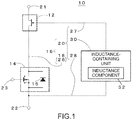
- Fig. 1 is an electric circuit diagram of a power device 10 common to each embodiment.
- the power device 10 is a device that is applied to a power source system of an electric vehicle using electric power as a drive source, for example, and the configuration and the application of the power device 10 are not limited to this example.
- the power device 10 is formed to include a normally-on type first transistor 12, a normally-off type second transistor 14, and an electric path 16 (more particularly, path portions 18, 20) forming a cascode connection between the first transistor 12 and the second transistor 14.
- the first transistor 12 includes a first gate (G), a first source (S), and a first drain (D)
- the second transistor 14 includes a second gate (G), a second source (S), and a second drain (D).
- the "normally-on type” means a type in which a current "flows" between a source (S) and a drain (D) under a condition where a voltage is not applied to a gate (G) (normal condition).
- the "normally-off type” means a type in which a current "does not flow” between the source (S) and the drain (D) under a condition where the voltage is not applied to the gate (G) (normal condition).
- the first transistor 12 includes a junction field effect transistor (JFET) using a wide band gap (WBG) semiconductor that is a GaN-based compound semiconductor containing gallium nitride (GaN), for example.
- the first transistor 12 may be a high electron mobility transistor (HEMT).
- JFET junction field effect transistor
- WBG wide band gap
- HEMT high electron mobility transistor
- the second transistor 14 includes a MOS (Metal-Oxide-Semiconductor)-type FET using silicon (Si), for example.
- MOS Metal-Oxide-Semiconductor
- a pn-junction-type parasitic diode 15 is interposed between the second source (S) and the second drain (D) of the second transistor 14.
- the first drain (D) of the first transistor 12, the second source (S) of the second transistor 14, and the second gate (G) of the second transistor 14 are connected to a drain terminal 21, a source terminal 22, and a gate terminal 23, respectively.
- the first source (S) of the first transistor 12 is connected to the second drain (D) of the second transistor 14 through a path portion 18.
- the first gate (G) of the first transistor 12 is connected to the second source (S) of the second transistor 14 through the path portion 20.
- the path portion 18 is comprised of a conductive electric wire 26 including a bonding wire 48 ( Figs. 3A and 3B ).
- the path portion 20 includes a conductive electric wire 27 that is connected to the first transistor 12, a conductive electric wire 28 that is connected to the second transistor 14, and an inductance-containing unit 30 that is disposed between the electric wires 27 and 28.
- an inductance-containing unit 30 may be provided on the path portion 18 side.
- the inductance-containing unit 30 may be directly connected to the first transistor 12 (the second transistor 14) without being connected by means of the electric wire 27 (28).
- the inductance-containing unit 30 is an inductance component 32 that is significantly larger than a parasitic inductance of the entire electric path 16 or includes the inductance component 32.
- unintentional minute inductances e.g., parasitic inductances of electric wires 26 to 28
- unintentional minute inductances e.g., parasitic inductances of electric wires 26 to 28
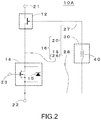
- An inductance-containing unit 30 of the power device 10A illustrated in Fig. 2 includes an inductor 40.
- an inductance component 32 is one inductor 40.
- Fig. 3A is a cross-sectional view illustrating an exemplified structure of a first transistor 12 in Fig. 2 . More particularly, Fig. 3A is an enlarged cross-sectional view of a main part including a gate electrode pad 46 of the first transistor 12.
- a well-known configuration disclosed in Japanese Patent Application Laid-Open No. 2008-66553 can be variously applied to the whole configuration of the power device 10A including the other portions.
- the first transistor 12 is formed by laminating a substrate 42, an electron transit layer 43, an electron supply layer 44, an interlayer insulation film 45, and a gate electrode pad 46 in this order from the lower side to the upper side in Fig. 3A .
- the first transistor 12 uses a GaN-based compound semiconductor, and typically, the substrate 42 is made of a material containing Si or SiC, the electron transit layer 43 is made of a material containing a non-doped GaN, the electron supply layer 44 is made of a material containing AlGaN (aluminum gallium nitride), and the interlayer insulation film 45 is made of a material containing SiO 2 (silicon dioxide).
- the gate electrode pad 46 is electrically connected to a lead frame (not illustrated) through a bonding wire 48 made of gold, silver, aluminum, etc.
- a magnetic thin film 50 is formed on the gate electrode pad 46, the magnetic thin film 50 functioning as the inductor 40 in Fig. 2 .
- the magnetic thin film 50 is formed of a magnetic body such as ferrite, using various well-known deposition methods including vapor deposition.
- the inductance component 32 may be a magnetic member that is formed on the gate electrode pad 46 included in the first transistor 12, and may be specifically the magnetic thin film 50.
- the efficient arrangement can be achieved with a small number of electronic elements, and therefore the device size and the manufacturing cost can be reduced.
- the inductance component 32 may be, for example, a microstrip line 53 having a meander structure that is formed on the gate electrode pad 46 included in the first transistor 12.
- the microstrip line 53 has a circuit structure that is formed of a conductive foil (GND) 56 formed on a bottom surface of a substrate 55, and linear conductive foils (transmission line) 54 formed on a top surface of the substrate 55.
- GND conductive foil
- transmission line linear conductive foils
- the inductance component 32 may be a portion of the electric wire 27 (28) included in the electric path 16.
- the electric wire 27 (28) is designed so that the portion of the electric wire 27 (28) has different thickness, length, line width or shape from that of the remaining portions of the electric wire 27 (28).
- the design method includes designing not only the thickness or length of the bonding wire 48 but also the length or line width of a wiring pattern (not illustrated).
- the inductance may be adjusted by changing the shape of the bonding wire 48 (e.g., by winding the bonding wire 48 into a coil shape). Even with this configuration, it is possible to achieve the same operation and effects as the configuration described above with a small number of electronic elements.
- An inductance-containing unit 30 of the power device 10B includes an inductor 60, a resistor 62 that is connected to the inductor 60 in series, a capacitor 64 and a resistor 66. Each of the capacitor 64 and the resistor 66 is connected in parallel to the series circuit of the inductor 60 and the resistor 62. In other words, an inductance component 32 is one inductor 60.
- the inductance-containing unit 30 is not limited to an L-circuit (first embodiment), and may be a combination circuit including the other electronic elements (R and/or C).
- the design flexibility of a switching circuit that takes measures against high frequency noise is enhanced as compared with the power device 10A of the first embodiment.
- the inductance-containing unit 30 may be formed by combining electronic components (including a function of L) each having a function of L, R or C, or may be formed of a material (a chip bead 52 of Fig. 5 ) having an electric property that can be expressed using an equivalent circuit model.
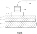
- Fig. 5 is a cross-sectional view illustrating an exemplified structure of a first transistor 12 in Fig. 4 .
- Fig. 5 is an enlarged cross-sectional view of a main part including a gate electrode pad 46 of the first transistor 12, similarly to Fig. 3A .
- a well-known configuration can be variously applied to the whole configuration of the power device 10B including the other portions.
- the first transistor 12 is formed by laminating a substrate 42, an electron transit layer 43, an electron supply layer 44, an interlayer insulation film 45, and a gate electrode pad 46 in this order from the lower side to the upper side in Fig. 5A .
- the gate electrode pad 46 is electrically connected to a lead frame (not illustrated) through a bonding wire 48.
- the chip bead 52 functioning as the inductor 60 and the resistor 62 (that are connected to each other in series) in Fig. 4 is disposed on the gate electrode pad 46.
- the tubular chip bead 52 is formed of a magnetic body such as ferrite, and the bonding wire 48 is inserted into the tubular chip bead 52.
- the chip bead 52 may have a laminate structure in which two types of magnetic sheets on which (a half of) a spiral conductor pattern is printed are alternately disposed.
- the inductance component 32 may be a magnetic member that is disposed on the gate electrode pad 46 included in the first transistor 12, and may be specifically the chip bead 52.
- the efficient arrangement can be achieved with a small number of electronic elements, and therefore the device size and the manufacturing cost can be reduced.
- the chip bead 52 is disposed on the gate electrode pad 46, but the arrangement is not limited to this specific example.
- the chip bead 52 may be disposed on a side of the electric wires 27, 28 between the first gate (G) of the first transistor 12 and the second source (S) of the second transistor 14, or may be disposed on a side of the path portion 18 between the first source (S) of the first transistor 12 and the second drain (D) of the second transistor 14.
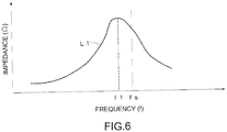
- Fig. 6 is a schematic graph showing a first effect by the inductance component 32, more particularly, is a graph showing a frequency characteristic of the power device 10B.
- the abscissa of the graph represents a frequency (f; Hz in unit), and the ordinate represents an impedance ( ⁇ in unit) of the inductance-containing unit 30.
- the impedance is adopted as a physical quantity (ordinate) of the "frequency characteristic," but the ordinate may represent an inductance (H in unit).
- This frequency characteristic L1 represents a band rejection filter having one peak centering on a peak frequency f1.
- the impedance is increased as the frequency comes closer to the peak frequency f1.
- the effect of suppressing or removing the surge is improved as the surge frequency fs comes closer to the peak frequency f1.
- a filtered voltage is applied to the cascode connection side containing the inductance component 32, and the filter includes a filter that reflects the frequency characteristic (L1) of the inductance component 32, and a high frequency filter that cuts off many frequency components belonging to the high frequency band.
- the inductance component 32 in an electric path (i.e., the path portion 20) between the first gate (G) of the first transistor 12 and the second source (S) of the second transistor 14.
- the inductance component 32 is thus disposed in the electric path, the effect of suppressing the surges of both the gate terminal 23 and the drain terminal 21 can be obtained without impairing the switching speed.
- Fig. 7A is a waveform chart of a drain voltage measured depending on the presence or absence of the inductance-containing unit 30
- Fig. 7B is a waveform chart of a gate current measured depending on the presence or absence of the inductance-containing unit 30.
- a graph indicated by a solid line shows a behavior that occurs when the inductance-containing unit 30 is "present,” and a graph indicated by a broken line shows a behavior that occurs when the inductance-containing unit 30 is "absent.” It is assumed that in a case where a power source is connected to the drain terminal 21, a GND is connected to the source terminal 22 and the gate terminal 23.
- An inductance-containing unit 30 of the power device 10C illustrated in Fig. 8 includes two inductors 70, 72 that are connected to each other in parallel, a diode 74 that is connected to the inductor 70 in series, and a diode 76 that is connected to the inductor 72 in series.
- the inductance component 32 comprises a plurality of (herein two) inductors 70, 72.
- An anode side of the diode 74 is connected to the inductor 70, and a cathode side of the diode 74 is connected to the second source (S) side of the second transistor 14.
- An anode side of the diode 76 is connected to the second source (S) side of the second transistor 14, and a cathode side of the diode 76 is connected to the inductor 72.
- the two diodes 74, 76 are connected to each other in parallel on the electric path 16 so that rectifying action directions of the two diodes 74, 76 do not coincide with each other, and the diodes 74, 76 are connected to the inductors 70, 72 in series, respectively.
- a plurality of inductors 70, 72 having different frequency characteristics are used to thereby enable high frequency filters different depending on charge/discharge direction to be selected by the rectifying actions of the diodes 74, 76.
- An inverse voltage of the inductors 70, 72 is reduced, thereby capable of preventing an excess voltage from being applied to the second source (S) of the second transistor 14.
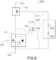
- An inductance-containing unit 30 of the power device 10D illustrated in Fig. 9 includes two inductors 80, 82 that are connected to each other in series.
- the inductance component 32 comprises a plurality of (two herein) inductors 80, 82.
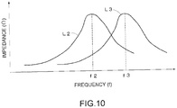
- the abscissa of the graph shown in Fig. 10 represents a frequency (f; Hz in unit), and the ordinate represents impedances ( ⁇ in unit) of the inductors 80, 82. Note that in an example of Fig. 10 , the impedance is adopted as a physical quantity (ordinate) of the "frequency characteristic," but the ordinate may represent an inductance (H in unit).
- the inductor 80 has a band rejection filter type frequency characteristic L2 having one peak centering on a peak frequency f2.
- the inductor 82 has a band rejection filter type frequency characteristic L3 having one peak centered on a peak frequency f3 (> f2).
- the impedance of the inductance-containing unit 30 is equivalent to a sum (L2 + L3) of both impedances.
- the power device 10 (10A to 10D) includes
- the inductance component 32 is provided in an electric path (the path portion 20) between the first gate (G) of the first transistor 12 and the second source (S) of the second transistor 14.
- the inductance component 32 is thus disposed in the electric path, the effect of suppressing the surges of both the gate terminal 23 and the drain terminal 21 can be obtained without impairing the switching speed.
- the inductance component 32 is comprised of the inductors 40, 60, 70, 72, 80, 82 having the frequency characteristic of suppressing or removing the surge that occurs along with the switching operation.
- the inductance component is hardly affected by the surge that occurs along with the switching operation.
Landscapes
- Electronic Switches (AREA)
- Semiconductor Integrated Circuits (AREA)
- Power Conversion In General (AREA)
- Metal-Oxide And Bipolar Metal-Oxide Semiconductor Integrated Circuits (AREA)
- Junction Field-Effect Transistors (AREA)
Abstract
Description
- The present invention relates to a power device formed by cascode-connecting a normally-on type first transistor and a normally-off type second transistor.
- Conventionally, there has been developed a moving body using electric power as a drive source, such as a power conversion device (hereinafter referred to as a "power device") suited to a power source system of an electric vehicle, for example. Recently, various mounting techniques have been proposed to achieve miniaturization and high efficiency while overcoming drawbacks encountered in a transistor using a wide band gap (WBG) semiconductor.
- In Japanese Patent No.
5012930 Fig. 1 ,Fig. 3 ,Fig. 5 to Fig. 8 , etc.), a device is proposed in which a normally-on type first transistor (SiC-JFET) is connected in cascode with a normally-off type second transistor (Si-MOSFET), and an RC circuit is provided between a gate of the first transistor and a source of the second transistor for regulating a switching speed. It is further disclosed that the switching loss can be reduced while suppressing occurrence of resonance (e.g., surge) by time control of the switching speed. - In such a power device, it is important to take measures against high frequency noise that occurs due to various causes in order to perform the stable switching operation at a high speed. Since it is unavoidable that the operation frequency of the power device increases along with the enhanced performance of an object (e.g., an electric vehicle) on which the power device is to be mounted, it is expected that the importance of the measures against noise are further increased.
- According to a control method proposed in Japanese Patent No.
5012930 - A further problem is that a circuit configuration disclosed in Japanese Patent No.
5012930 - As another measure against surge in prior art, ferrite beads are inserted into a gate of the cascode circuit to suppress the surge of the gate, thereby also suppressing the surge of the drain current. However, in a device using a GaN-based compound semiconductor, even when the ferrite beads are inserted into the gate of the cascode circuit, rather than suppressing the surge of the gate, the surge of the drain current is increased, so that the effect of suppressing the surge cannot be sufficiently obtained as the entire circuit.
- The present invention has been made in view of the above described problems, and it is an object of the present invention to provide a power device capable of easily designing a switching circuit that takes measures against high frequency noise while maintaining a switching speed without change.
- A "power device" according to the present invention comprises:
- a normally-on type first transistor that uses a GaN-based compound semiconductor, the normally-on type first transistor including a first gate, a first source, and a first drain;
- a normally-off type second transistor including a second gate, a second source, and a second drain; and
- an electric path that forms cascode connections between the first gate of the first transistor and the second source of the second transistor, and between the first source of the first transistor and the second drain of the second transistor, and contains an inductance component between the first transistor and the second transistor.
- Since the electric path forming the cascode connection between the first transistor and the second transistor contains an inductance component as described above, a filtered voltage is applied to the cascode connection side, and the filter includes a filter that reflects the frequency characteristic of the inductance component, and a high frequency filter that cuts off many frequency components belonging to the high frequency band. Even when the frequency of the noise component to be addressed is increased, it is not necessary to greatly change the filter as long as the frequency is higher than a cutoff frequency. Thus, it is possible to easily design the switching circuit that takes measures against high frequency noise while maintaining the high switching speed without change.
- It is more preferable to provide the inductance component in the electric path between the first gate of the first transistor and the second source of the second transistor. When the inductance component is thus disposed in the electric path, the effect of suppressing the surges of both of the gate terminal and the drain terminal can be obtained without impairing the switching speed.
- It is preferable that the inductance component is an inductor having the frequency characteristic of suppressing or removing the surge that occurs along with the switching operation. Thus, the inductance component is hardly affected by the surge that occurs along with the switching operation.
- It is preferable that the inductance component comprises a plurality of inductors having the frequency characteristics different from each other, the plurality of inductors are connected to each other in parallel on the electric path, and a plurality of diodes of which rectifying action directions do not coincide with each other are connected to the respective plurality of inductors in series. The high frequency filters different depending on the charge/discharge direction can be selected by the rectifying actions of the diodes. An inverse voltage of the inductors is reduced, thereby capable of preventing an excess voltage from being applied to the second source of the second transistor.
- It is preferable that the inductance component comprises a plurality of inductors having the frequency characteristics different from each other, and the plurality of inductors are connected to each other in series on the electric path. The ranges of the frequency characteristics can be mutually covered, as a result, an effective band width of the high frequency filter can be substantially increased.
- It is preferable that the inductance component be a magnetic member that is disposed or formed on a gate electrode pad included in the first transistor. Alternatively, it is also preferable that the inductance component is a microstrip line that is formed on the gate electrode pad included in the first transistor. Alternatively, it is also preferable that the inductance component is a portion of an electric wire included in the electric path, and the portion of the electric wire has different thickness, length, line width or shape from that of the remaining portions of the electric wire.
- In each embodiment, the efficient arrangement can be achieved with a small number of electronic elements, and therefore the device size and the manufacturing cost can be reduced.
- According to a power device of the present invention, it is possible to easily design a switching circuit that takes measures against high frequency noise while maintaining a high switching speed without change.
-
-
Fig. 1 is an electric circuit diagram of a power device common to each embodiment. -
Fig. 2 is an electric circuit diagram of a power device according to a first embodiment. -
Fig. 3A and Fig. 3B each are a cross-sectional view illustrating an exemplified structure of a first transistor inFig. 2 . -
Fig. 4 is an electric circuit diagram of a power device according to a second embodiment. -
Fig. 5 is a cross-sectional view illustrating an exemplified structure of a first transistor inFig. 4 . -
Fig. 6 is a schematic graph showing a first effect by an inductance component. -
Fig. 7A and Fig. 7B each are a schematic graph showing a second effect by an inductance component. -
Fig. 8 is an electric circuit diagram of a power device according to a third embodiment. -
Fig. 9 is an electric circuit diagram of a power device according to a fourth embodiment. -
Fig. 10 is a schematic graph showing a frequency characteristic of each inductor ofFig. 9 . - Hereinafter, preferable embodiments of a power device according to the present invention will be described with reference to the accompanying drawings.
-
Fig. 1 is an electric circuit diagram of apower device 10 common to each embodiment. Thepower device 10 is a device that is applied to a power source system of an electric vehicle using electric power as a drive source, for example, and the configuration and the application of thepower device 10 are not limited to this example. - The
power device 10 is formed to include a normally-on typefirst transistor 12, a normally-off typesecond transistor 14, and an electric path 16 (more particularly,path portions 18, 20) forming a cascode connection between thefirst transistor 12 and thesecond transistor 14. Thefirst transistor 12 includes a first gate (G), a first source (S), and a first drain (D), and thesecond transistor 14 includes a second gate (G), a second source (S), and a second drain (D). - As used herein, the "normally-on type" means a type in which a current "flows" between a source (S) and a drain (D) under a condition where a voltage is not applied to a gate (G) (normal condition). In contrast, the "normally-off type" means a type in which a current "does not flow" between the source (S) and the drain (D) under a condition where the voltage is not applied to the gate (G) (normal condition).
- The
first transistor 12 includes a junction field effect transistor (JFET) using a wide band gap (WBG) semiconductor that is a GaN-based compound semiconductor containing gallium nitride (GaN), for example. Alternatively, thefirst transistor 12 may be a high electron mobility transistor (HEMT). - The
second transistor 14 includes a MOS (Metal-Oxide-Semiconductor)-type FET using silicon (Si), for example. A pn-junction-typeparasitic diode 15 is interposed between the second source (S) and the second drain (D) of thesecond transistor 14. - As understood from
Fig. 1 , the first drain (D) of thefirst transistor 12, the second source (S) of thesecond transistor 14, and the second gate (G) of thesecond transistor 14 are connected to adrain terminal 21, asource terminal 22, and agate terminal 23, respectively. The first source (S) of thefirst transistor 12 is connected to the second drain (D) of thesecond transistor 14 through apath portion 18. The first gate (G) of thefirst transistor 12 is connected to the second source (S) of thesecond transistor 14 through thepath portion 20. - The
path portion 18 is comprised of a conductiveelectric wire 26 including a bonding wire 48 (Figs. 3A and 3B ). Thepath portion 20 includes a conductiveelectric wire 27 that is connected to thefirst transistor 12, a conductiveelectric wire 28 that is connected to thesecond transistor 14, and an inductance-containingunit 30 that is disposed between theelectric wires unit 30, an inductance-containingunit 30 may be provided on thepath portion 18 side. The inductance-containingunit 30 may be directly connected to the first transistor 12 (the second transistor 14) without being connected by means of the electric wire 27 (28). - The inductance-containing
unit 30 is aninductance component 32 that is significantly larger than a parasitic inductance of the entireelectric path 16 or includes theinductance component 32. Thus, note that unintentional minute inductances (e.g., parasitic inductances ofelectric wires 26 to 28) on circuit design are not contained in theinductance component 32. - A configuration of a power device 10A according to a first embodiment will be described with reference to
Figs. 2 ,3A and Fig. 3B . An inductance-containingunit 30 of the power device 10A illustrated inFig. 2 includes aninductor 40. In other words, aninductance component 32 is oneinductor 40. -
Fig. 3A is a cross-sectional view illustrating an exemplified structure of afirst transistor 12 inFig. 2 . More particularly,Fig. 3A is an enlarged cross-sectional view of a main part including agate electrode pad 46 of thefirst transistor 12. A well-known configuration disclosed in Japanese Patent Application Laid-Open No.2008-66553 - The
first transistor 12 is formed by laminating asubstrate 42, anelectron transit layer 43, anelectron supply layer 44, aninterlayer insulation film 45, and agate electrode pad 46 in this order from the lower side to the upper side inFig. 3A . Thefirst transistor 12 uses a GaN-based compound semiconductor, and typically, thesubstrate 42 is made of a material containing Si or SiC, theelectron transit layer 43 is made of a material containing a non-doped GaN, theelectron supply layer 44 is made of a material containing AlGaN (aluminum gallium nitride), and theinterlayer insulation film 45 is made of a material containing SiO2 (silicon dioxide). - The
gate electrode pad 46 is electrically connected to a lead frame (not illustrated) through abonding wire 48 made of gold, silver, aluminum, etc. A magneticthin film 50 is formed on thegate electrode pad 46, the magneticthin film 50 functioning as theinductor 40 inFig. 2 . The magneticthin film 50 is formed of a magnetic body such as ferrite, using various well-known deposition methods including vapor deposition. - Thus, the
inductance component 32 may be a magnetic member that is formed on thegate electrode pad 46 included in thefirst transistor 12, and may be specifically the magneticthin film 50. In this case, the efficient arrangement can be achieved with a small number of electronic elements, and therefore the device size and the manufacturing cost can be reduced. - As illustrated in
Fig. 3B , theinductance component 32 may be, for example, amicrostrip line 53 having a meander structure that is formed on thegate electrode pad 46 included in thefirst transistor 12. Themicrostrip line 53 has a circuit structure that is formed of a conductive foil (GND) 56 formed on a bottom surface of asubstrate 55, and linear conductive foils (transmission line) 54 formed on a top surface of thesubstrate 55. Even with this configuration, it is possible to achieve the same operation and effects as the configuration described above with a small number of electronic elements. - The
inductance component 32 may be a portion of the electric wire 27 (28) included in theelectric path 16. In this case, the electric wire 27 (28) is designed so that the portion of the electric wire 27 (28) has different thickness, length, line width or shape from that of the remaining portions of the electric wire 27 (28). Specifically, the design method includes designing not only the thickness or length of thebonding wire 48 but also the length or line width of a wiring pattern (not illustrated). The inductance may be adjusted by changing the shape of the bonding wire 48 (e.g., by winding thebonding wire 48 into a coil shape). Even with this configuration, it is possible to achieve the same operation and effects as the configuration described above with a small number of electronic elements. - Since an impedance of the
inductor 40 is higher on a high frequency side, a surge having a frequency higher than a switching frequency can be prevented from occurring without obstructing the switching of the power device 10A. - A power device 10B according to a second embodiment will be described with reference to
Fig. 4 andFig. 5 . An inductance-containingunit 30 of the power device 10B includes aninductor 60, aresistor 62 that is connected to theinductor 60 in series, acapacitor 64 and aresistor 66. Each of thecapacitor 64 and theresistor 66 is connected in parallel to the series circuit of theinductor 60 and theresistor 62. In other words, aninductance component 32 is oneinductor 60. - Thus, the inductance-containing
unit 30 is not limited to an L-circuit (first embodiment), and may be a combination circuit including the other electronic elements (R and/or C). The design flexibility of a switching circuit that takes measures against high frequency noise is enhanced as compared with the power device 10A of the first embodiment. - Note that the inductance-containing unit 30 (
Fig. 4 ) may be formed by combining electronic components (including a function of L) each having a function of L, R or C, or may be formed of a material (achip bead 52 ofFig. 5 ) having an electric property that can be expressed using an equivalent circuit model. -
Fig. 5 is a cross-sectional view illustrating an exemplified structure of afirst transistor 12 inFig. 4 .Fig. 5 is an enlarged cross-sectional view of a main part including agate electrode pad 46 of thefirst transistor 12, similarly toFig. 3A . As described above, a well-known configuration can be variously applied to the whole configuration of the power device 10B including the other portions. - The
first transistor 12 is formed by laminating asubstrate 42, anelectron transit layer 43, anelectron supply layer 44, aninterlayer insulation film 45, and agate electrode pad 46 in this order from the lower side to the upper side inFig. 5A . Thegate electrode pad 46 is electrically connected to a lead frame (not illustrated) through abonding wire 48. Thechip bead 52 functioning as theinductor 60 and the resistor 62 (that are connected to each other in series) inFig. 4 is disposed on thegate electrode pad 46. - The
tubular chip bead 52 is formed of a magnetic body such as ferrite, and thebonding wire 48 is inserted into thetubular chip bead 52. Note that thechip bead 52 may have a laminate structure in which two types of magnetic sheets on which (a half of) a spiral conductor pattern is printed are alternately disposed. - Thus, the
inductance component 32 may be a magnetic member that is disposed on thegate electrode pad 46 included in thefirst transistor 12, and may be specifically thechip bead 52. In this case, the efficient arrangement can be achieved with a small number of electronic elements, and therefore the device size and the manufacturing cost can be reduced. - Note that in
Fig. 5 , thechip bead 52 is disposed on thegate electrode pad 46, but the arrangement is not limited to this specific example. For example, thechip bead 52 may be disposed on a side of theelectric wires first transistor 12 and the second source (S) of thesecond transistor 14, or may be disposed on a side of thepath portion 18 between the first source (S) of thefirst transistor 12 and the second drain (D) of thesecond transistor 14. - An effect by the
inductance component 32 whereby surges are suppressed will be described with reference toFig. 6 from the viewpoint of the frequency characteristic. For example, it is assumed that surge occurs in a voltage or current waveform along with the switching operation of the power device 10B. This surge waveform has a frequency characteristic (a so-called power spectrum) including a surge frequency fs as a principal component. -
Fig. 6 is a schematic graph showing a first effect by theinductance component 32, more particularly, is a graph showing a frequency characteristic of the power device 10B. The abscissa of the graph represents a frequency (f; Hz in unit), and the ordinate represents an impedance (Ω in unit) of the inductance-containingunit 30. Note that in an example ofFig. 6 , the impedance is adopted as a physical quantity (ordinate) of the "frequency characteristic," but the ordinate may represent an inductance (H in unit). - This frequency characteristic L1 represents a band rejection filter having one peak centering on a peak frequency f1. The impedance is increased as the frequency comes closer to the peak frequency f1. Thus, the effect of suppressing or removing the surge is improved as the surge frequency fs comes closer to the peak frequency f1. If the surge frequency fs is thus known, it is desirable to introduce the inductance-containing
unit 30 having the frequency characteristic L1 in which a value of a frequency difference |fs-f1| is close to zero. - As described above, a filtered voltage is applied to the cascode connection side containing the
inductance component 32, and the filter includes a filter that reflects the frequency characteristic (L1) of theinductance component 32, and a high frequency filter that cuts off many frequency components belonging to the high frequency band. - Even when the frequency of the noise component to be addressed is increased, it is not necessary to greatly change the filter as long as the frequency is higher than a cutoff frequency. Thus, it is possible to easily design the switching circuit that takes measures against high frequency noise while maintaining the high switching speed without change.
- It is preferable to provide the
inductance component 32 in an electric path (i.e., the path portion 20) between the first gate (G) of thefirst transistor 12 and the second source (S) of thesecond transistor 14. When theinductance component 32 is thus disposed in the electric path, the effect of suppressing the surges of both thegate terminal 23 and thedrain terminal 21 can be obtained without impairing the switching speed. - The surge suppressing effect by the
inductance component 32 will be described with reference toFigs. 7A and 7B from the viewpoint of the waveforms. More particularly,Fig. 7A is a waveform chart of a drain voltage measured depending on the presence or absence of the inductance-containingunit 30, andFig. 7B is a waveform chart of a gate current measured depending on the presence or absence of the inductance-containingunit 30. - A graph indicated by a solid line shows a behavior that occurs when the inductance-containing
unit 30 is "present," and a graph indicated by a broken line shows a behavior that occurs when the inductance-containingunit 30 is "absent." It is assumed that in a case where a power source is connected to thedrain terminal 21, a GND is connected to thesource terminal 22 and thegate terminal 23. - As shown in
Fig. 7A , when the switching operation from an "ON state" to an "OFF state" is started, the drain voltage rapidly rises from the GND (0 V), and comes closer to a steady-state value while attenuating vibration. As understood fromFig. 7A , the surge when the inductance-containingunit 30 is "present" is significantly suppressed as compared with that when the inductance-containingunit 30 is "absent." - As shown in
Fig. 7B , when the switching operation from an "ON state" to an "OFF state" is started, the gate current rapidly rises from the steady-state value, and comes closer to an original value (the steady-state value) while attenuating vibration. As is understood fromFig. 7B , the surge when the inductance-containingunit 30 is "present" is significantly suppressed as compared with that when the inductance-containingunit 30 is "absent." - When such a configuration of the power device 10B is adopted, a filter effect of suppressing high frequency noise due to a surge can be obtained. Note that the above-described operation and effects can be obtained not only in the embodiment of the power device 10B but also in the other embodiments.
- A
power device 10C according to a third embodiment will be described with reference toFig. 8 . An inductance-containingunit 30 of thepower device 10C illustrated inFig. 8 includes twoinductors diode 74 that is connected to theinductor 70 in series, and adiode 76 that is connected to theinductor 72 in series. In other words, theinductance component 32 comprises a plurality of (herein two)inductors - An anode side of the
diode 74 is connected to theinductor 70, and a cathode side of thediode 74 is connected to the second source (S) side of thesecond transistor 14. An anode side of thediode 76 is connected to the second source (S) side of thesecond transistor 14, and a cathode side of thediode 76 is connected to theinductor 72. In other words, the twodiodes electric path 16 so that rectifying action directions of the twodiodes diodes inductors - A plurality of
inductors diodes inductors second transistor 14. - A power device 10D according to a fourth embodiment will be described with reference to
Fig. 9 andFig. 10 . An inductance-containingunit 30 of the power device 10D illustrated inFig. 9 includes twoinductors inductance component 32 comprises a plurality of (two herein)inductors - The abscissa of the graph shown in
Fig. 10 represents a frequency (f; Hz in unit), and the ordinate represents impedances (Ω in unit) of theinductors Fig. 10 , the impedance is adopted as a physical quantity (ordinate) of the "frequency characteristic," but the ordinate may represent an inductance (H in unit). - The
inductor 80 has a band rejection filter type frequency characteristic L2 having one peak centering on a peak frequency f2. Theinductor 82 has a band rejection filter type frequency characteristic L3 having one peak centered on a peak frequency f3 (> f2). In this case, the impedance of the inductance-containingunit 30 is equivalent to a sum (L2 + L3) of both impedances. - When a plurality of (two herein)
inductors electric path 16, the ranges of the frequency characteristics can be mutually covered. As a result, an effective band width of the high frequency filter can be substantially increased. - As described above, the power device 10 (10A to 10D) includes
- [1] a normally-on type
first transistor 12 that uses a GaN-based compound semiconductor, the normally-on typefirst transistor 12 including a first gate (G), a first source (S), and a first drain (D), - [2] a normally-off type
second transistor 14 including a second gate (G), a second source (S), and a second drain (D), and - [3] an
electric path 16 that forms cascode connections between the first gate (G) of thefirst transistor 12 and the second source (S) of thesecond transistor 14, and between the first source (S) of thefirst transistor 12 and the second drain (D) of thesecond transistor 14, and contains an inductance-containingunit 30 between thefirst transistor 12 and thesecond transistor 14. Since theelectric path 16 forming the cascode connection between thefirst transistor 12 and thesecond transistor 14 contains aninductance component 32, a filtered voltage is applied to the cascode connection side, and the filter includes a filter that reflects the frequency characteristic of theinductance component 32, and a high frequency filter that cuts off many frequency components belonging to the high frequency band. - Even when the frequency of the noise component to be addressed is increased, it is not necessary to greatly change the filter as long as the frequency is higher than a cutoff frequency. Thus, it is possible to easily design the switching circuit that takes measures against high frequency noise while maintaining the high switching speed without change.
- It is more preferable to provide the
inductance component 32 in an electric path (the path portion 20) between the first gate (G) of thefirst transistor 12 and the second source (S) of thesecond transistor 14. When theinductance component 32 is thus disposed in the electric path, the effect of suppressing the surges of both thegate terminal 23 and thedrain terminal 21 can be obtained without impairing the switching speed. - It is preferable that the
inductance component 32 is comprised of theinductors - Note that the present invention is not limited to the above-described embodiments, and can be freely changed without departing from the scope of the invention. The respective configurations in the embodiments described above can be appropriately combined as long as a technical inconsistency does not occur, for example.
-
- 10 (A/B/C/D) power device,
- 12 first transistor,
- 14 second transistor,
- 15 parasitic diode,
- 16 electric path,
- 18, 20 path portion,
- 21 drain terminal,
- 22 source terminal,
- 23 gate terminal,
- 26 to 28 electric wire,
- 30 inductance-containing unit,
- 32 inductance component,
- 40, 60, 70, 72, 80, 82 inductor,
- 42 substrate,
- 43 electron transit layer,
- 44 electron supply layer,
- 46 gate electrode pad,
- 48 bonding wire (electric wire),
- 50 magnetic thin film (magnetic member),
- 52 chip bead (magnetic member),
- 53 microstrip line,
- 54 conductive foil (transmission line),
- 55 substrate,
- 56 conductive foil (GND),
- 62, 66 resistor,
- 74, 76 diode
Claims (7)
- A power device comprising:a normally-on type first transistor that uses a GaN-based compound semiconductor, the normally-on type first transistor including a first gate, a first source, and a first drain;a normally-off type second transistor including a second gate, a second source, and a second drain; andan electric path that forms cascode connections between the first gate of the first transistor and the second source of the second transistor, and between the first source of the first transistor and the second drain of the second transistor, and contains an inductance component between the first transistor and the second transistor.
- The power device according to claim 1, wherein
the inductance component is provided in the electric path between the first gate of the first transistor and the second source of the second transistor. - The power device according to claim 2, wherein
the inductance component is an inductor having a frequency characteristic of suppressing or removing a surge that occurs along with a switching operation. - The power device according to claim 3, wherein
the inductance component comprises a plurality of inductors having the frequency characteristics different from each other,
the plurality of inductors are connected to each other in parallel on the electric path, and
a plurality of diodes of which rectifying action directions do not coincide with each other are connected to the respective plurality of inductors in series. - The power device according to claim 3, wherein
the inductance component comprises a plurality of inductors having the frequency characteristics different from each other, and
the plurality of inductors are connected to each other in series on the electric path. - The power device according to any one of claims 1 to 5, wherein
the inductance component is a magnetic member that is disposed or formed on a gate electrode pad included in the first transistor. - The power device according to any one of claims 1 to 5, wherein
the inductance component is a microstrip line that is formed on a gate electrode pad included in the first transistor.
Applications Claiming Priority (2)
| Application Number | Priority Date | Filing Date | Title |
|---|---|---|---|
| JP2015178375 | 2015-09-10 | ||
| PCT/JP2016/076540 WO2017043611A1 (en) | 2015-09-10 | 2016-09-09 | Power device |
Publications (2)
| Publication Number | Publication Date |
|---|---|
| EP3349358A1 true EP3349358A1 (en) | 2018-07-18 |
| EP3349358A4 EP3349358A4 (en) | 2019-04-17 |
Family
ID=58239910
Family Applications (1)
| Application Number | Title | Priority Date | Filing Date |
|---|---|---|---|
| EP16844472.7A Withdrawn EP3349358A4 (en) | 2015-09-10 | 2016-09-09 | ELECTRICAL DEVICE |
Country Status (5)
| Country | Link |
|---|---|
| US (1) | US20180174986A1 (en) |
| EP (1) | EP3349358A4 (en) |
| JP (1) | JPWO2017043611A1 (en) |
| CN (1) | CN107925404A (en) |
| WO (1) | WO2017043611A1 (en) |
Families Citing this family (2)
| Publication number | Priority date | Publication date | Assignee | Title |
|---|---|---|---|---|
| JP7224918B2 (en) | 2019-01-04 | 2023-02-20 | 株式会社東芝 | Semiconductor devices and semiconductor packages |
| EP4044225B1 (en) * | 2021-02-16 | 2024-06-26 | Nexperia B.V. | A semiconductor device and a method of manufacturing a semiconductor device |
Family Cites Families (21)
| Publication number | Priority date | Publication date | Assignee | Title |
|---|---|---|---|---|
| JPS5546068B2 (en) * | 1973-05-22 | 1980-11-21 | ||
| DE19902520B4 (en) * | 1999-01-22 | 2005-10-06 | Siemens Ag | Hybrid power MOSFET |
| DE102005051571B4 (en) * | 2005-10-21 | 2013-06-20 | Fraunhofer-Gesellschaft zur Förderung der angewandten Forschung e.V. | Photodiode chip high cutoff frequency |
| CH700697A2 (en) * | 2009-03-27 | 2010-09-30 | Eth Zuerich | SWITCHING DEVICE WITH A cascade circuit. |
| CN102725840B (en) * | 2010-01-25 | 2014-12-10 | 夏普株式会社 | Composite semiconductor device |
| JP5012930B2 (en) * | 2010-02-15 | 2012-08-29 | 株式会社デンソー | Hybrid power device |
| US9859882B2 (en) * | 2011-03-21 | 2018-01-02 | Infineon Technologies Americas Corp. | High voltage composite semiconductor device with protection for a low voltage device |
| US9236376B2 (en) * | 2011-03-21 | 2016-01-12 | Infineon Technologies Americas Corp. | Power semiconductor device with oscillation prevention |
| US8766375B2 (en) * | 2011-03-21 | 2014-07-01 | International Rectifier Corporation | Composite semiconductor device with active oscillation prevention |
| US9343440B2 (en) * | 2011-04-11 | 2016-05-17 | Infineon Technologies Americas Corp. | Stacked composite device including a group III-V transistor and a group IV vertical transistor |
| JP5290354B2 (en) * | 2011-05-06 | 2013-09-18 | シャープ株式会社 | Semiconductor device and electronic equipment |
| JP2013042270A (en) * | 2011-08-12 | 2013-02-28 | Advanced Power Device Research Association | Transistor circuit, bidirectional switch circuit, diode circuit, and method of manufacturing transistor circuit |
| WO2013046439A1 (en) * | 2011-09-30 | 2013-04-04 | ルネサスエレクトロニクス株式会社 | Semiconductor device |
| JP5813781B2 (en) * | 2011-11-24 | 2015-11-17 | シャープ株式会社 | Semiconductor device and electronic equipment |
| WO2013146570A1 (en) * | 2012-03-27 | 2013-10-03 | シャープ株式会社 | Cascode circuit |
| US20150340997A1 (en) * | 2012-11-09 | 2015-11-26 | Mitsubishi Electric Corporation | Cascode amplifier |
| US9171837B2 (en) * | 2012-12-17 | 2015-10-27 | Nxp B.V. | Cascode circuit |
| WO2014094115A1 (en) * | 2012-12-21 | 2014-06-26 | Gan Systems Inc. | Devices and systems comprising drivers for power conversion circuits |
| US9099441B2 (en) * | 2013-02-05 | 2015-08-04 | Infineon Technologies Austria Ag | Power transistor arrangement and method for manufacturing the same |
| JP6223729B2 (en) * | 2013-06-25 | 2017-11-01 | 株式会社東芝 | Semiconductor device |
| KR102178865B1 (en) * | 2015-02-25 | 2020-11-18 | 한국전자통신연구원 | Switch circuit of cascode type having high speed switching performance |
-
2016
- 2016-09-09 CN CN201680046927.6A patent/CN107925404A/en active Pending
- 2016-09-09 WO PCT/JP2016/076540 patent/WO2017043611A1/en not_active Ceased
- 2016-09-09 JP JP2017538529A patent/JPWO2017043611A1/en active Pending
- 2016-09-09 EP EP16844472.7A patent/EP3349358A4/en not_active Withdrawn
-
2018
- 2018-02-15 US US15/897,925 patent/US20180174986A1/en not_active Abandoned
Also Published As
| Publication number | Publication date |
|---|---|
| US20180174986A1 (en) | 2018-06-21 |
| JPWO2017043611A1 (en) | 2018-06-21 |
| EP3349358A4 (en) | 2019-04-17 |
| WO2017043611A1 (en) | 2017-03-16 |
| CN107925404A (en) | 2018-04-17 |
Similar Documents
| Publication | Publication Date | Title |
|---|---|---|
| CN103325828B (en) | Nitride semiconductor device | |
| JP7224918B2 (en) | Semiconductor devices and semiconductor packages | |
| US9543940B2 (en) | Switching circuits having ferrite beads | |
| EP2819161A2 (en) | Semiconductor device | |
| KR102178865B1 (en) | Switch circuit of cascode type having high speed switching performance | |
| US10897249B1 (en) | Switching circuits having drain connected ferrite beads | |
| US10886730B2 (en) | Filter having an ESD protection device | |
| US10200030B2 (en) | Paralleling of switching devices for high power circuits | |
| US20180174986A1 (en) | Power device | |
| JP4807141B2 (en) | Semiconductor device | |
| KR102463221B1 (en) | Power Semiconductor Module | |
| US9768099B1 (en) | IC package with integrated inductor | |
| JP2016213344A (en) | Noise suppression parts | |
| JP6173528B1 (en) | Power converter | |
| WO2023145316A1 (en) | Semiconductor device and semiconductor module | |
| JP2008283594A (en) | EMI filter | |
| JP2025176835A (en) | Drivers, signal transmission devices, electronic devices, vehicles | |
| JP2026000567A (en) | Signal transmission devices, electronic devices, vehicles, insulated gate driver ICs | |
| WO2021240990A1 (en) | Semiconductor device, semiconductor module, and electronic apparatus | |
| CN114097080A (en) | Nitride based multi-channel switching semiconductor device and method of manufacturing the same | |
| JP2002124631A (en) | Semiconductor integrated circuit and surge-protecting circuit |
Legal Events
| Date | Code | Title | Description |
|---|---|---|---|
| STAA | Information on the status of an ep patent application or granted ep patent |
Free format text: STATUS: THE INTERNATIONAL PUBLICATION HAS BEEN MADE |
|
| PUAI | Public reference made under article 153(3) epc to a published international application that has entered the european phase |
Free format text: ORIGINAL CODE: 0009012 |
|
| STAA | Information on the status of an ep patent application or granted ep patent |
Free format text: STATUS: REQUEST FOR EXAMINATION WAS MADE |
|
| 17P | Request for examination filed |
Effective date: 20180403 |
|
| AK | Designated contracting states |
Kind code of ref document: A1 Designated state(s): AL AT BE BG CH CY CZ DE DK EE ES FI FR GB GR HR HU IE IS IT LI LT LU LV MC MK MT NL NO PL PT RO RS SE SI SK SM TR |
|
| AX | Request for extension of the european patent |
Extension state: BA ME |
|
| DAV | Request for validation of the european patent (deleted) | ||
| DAX | Request for extension of the european patent (deleted) | ||
| A4 | Supplementary search report drawn up and despatched |
Effective date: 20190314 |
|
| RIC1 | Information provided on ipc code assigned before grant |
Ipc: H01L 49/02 20060101ALN20190308BHEP Ipc: H01L 27/088 20060101ALI20190308BHEP Ipc: H03K 17/16 20060101AFI20190308BHEP Ipc: H01L 27/06 20060101ALI20190308BHEP Ipc: H01L 21/8258 20060101ALN20190308BHEP Ipc: H01L 23/64 20060101ALN20190308BHEP Ipc: H03K 17/10 20060101ALI20190308BHEP Ipc: H01L 23/66 20060101ALN20190308BHEP Ipc: H01L 27/02 20060101ALN20190308BHEP Ipc: H01L 21/02 20060101ALN20190308BHEP Ipc: H01L 21/8232 20060101ALI20190308BHEP Ipc: H01L 29/20 20060101ALN20190308BHEP Ipc: H01L 29/205 20060101ALN20190308BHEP Ipc: H01L 21/8234 20060101ALI20190308BHEP Ipc: H03K 17/687 20060101ALI20190308BHEP Ipc: H01P 3/08 20060101ALN20190308BHEP |
|
| STAA | Information on the status of an ep patent application or granted ep patent |
Free format text: STATUS: EXAMINATION IS IN PROGRESS |
|
| 17Q | First examination report despatched |
Effective date: 20210209 |
|
| STAA | Information on the status of an ep patent application or granted ep patent |
Free format text: STATUS: THE APPLICATION HAS BEEN WITHDRAWN |
|
| 18W | Application withdrawn |
Effective date: 20210607 |