EP3349239A1 - Semiconductor device production method, and semiconductor device - Google Patents
Semiconductor device production method, and semiconductor device Download PDFInfo
- Publication number
- EP3349239A1 EP3349239A1 EP16909740.9A EP16909740A EP3349239A1 EP 3349239 A1 EP3349239 A1 EP 3349239A1 EP 16909740 A EP16909740 A EP 16909740A EP 3349239 A1 EP3349239 A1 EP 3349239A1
- Authority
- EP
- European Patent Office
- Prior art keywords
- semiconductor device
- semiconductor
- layer
- exposed
- glass
- Prior art date
- Legal status (The legal status is an assumption and is not a legal conclusion. Google has not performed a legal analysis and makes no representation as to the accuracy of the status listed.)
- Granted
Links
Images




Classifications
-
- H—ELECTRICITY
- H10—SEMICONDUCTOR DEVICES; ELECTRIC SOLID-STATE DEVICES NOT OTHERWISE PROVIDED FOR
- H10W—GENERIC PACKAGES, INTERCONNECTIONS, CONNECTORS OR OTHER CONSTRUCTIONAL DETAILS OF DEVICES COVERED BY CLASS H10
- H10W74/00—Encapsulations, e.g. protective coatings
- H10W74/10—Encapsulations, e.g. protective coatings characterised by their shape or disposition
- H10W74/131—Encapsulations, e.g. protective coatings characterised by their shape or disposition the semiconductor body being only partially enclosed
- H10W74/134—Encapsulations, e.g. protective coatings characterised by their shape or disposition the semiconductor body being only partially enclosed the encapsulations being in grooves in the semiconductor body
-
- H—ELECTRICITY
- H10—SEMICONDUCTOR DEVICES; ELECTRIC SOLID-STATE DEVICES NOT OTHERWISE PROVIDED FOR
- H10D—INORGANIC ELECTRIC SEMICONDUCTOR DEVICES
- H10D62/00—Semiconductor bodies, or regions thereof, of devices having potential barriers
- H10D62/10—Shapes, relative sizes or dispositions of the regions of the semiconductor bodies; Shapes of the semiconductor bodies
- H10D62/102—Constructional design considerations for preventing surface leakage or controlling electric field concentration
- H10D62/112—Constructional design considerations for preventing surface leakage or controlling electric field concentration for preventing surface leakage due to surface inversion layers, e.g. by using channel stoppers
-
- H—ELECTRICITY
- H10—SEMICONDUCTOR DEVICES; ELECTRIC SOLID-STATE DEVICES NOT OTHERWISE PROVIDED FOR
- H10D—INORGANIC ELECTRIC SEMICONDUCTOR DEVICES
- H10D8/00—Diodes
- H10D8/01—Manufacture or treatment
- H10D8/045—Manufacture or treatment of PN junction diodes
-
- H—ELECTRICITY
- H10—SEMICONDUCTOR DEVICES; ELECTRIC SOLID-STATE DEVICES NOT OTHERWISE PROVIDED FOR
- H10D—INORGANIC ELECTRIC SEMICONDUCTOR DEVICES
- H10D8/00—Diodes
- H10D8/411—PN diodes having planar bodies
-
- H—ELECTRICITY
- H10—SEMICONDUCTOR DEVICES; ELECTRIC SOLID-STATE DEVICES NOT OTHERWISE PROVIDED FOR
- H10D—INORGANIC ELECTRIC SEMICONDUCTOR DEVICES
- H10D8/00—Diodes
- H10D8/422—PN diodes having the PN junctions in mesas
-
- H—ELECTRICITY
- H10—SEMICONDUCTOR DEVICES; ELECTRIC SOLID-STATE DEVICES NOT OTHERWISE PROVIDED FOR
- H10P—GENERIC PROCESSES OR APPARATUS FOR THE MANUFACTURE OR TREATMENT OF DEVICES COVERED BY CLASS H10
- H10P34/00—Irradiation with electromagnetic or particle radiation of wafers, substrates or parts of devices
- H10P34/40—Irradiation with electromagnetic or particle radiation of wafers, substrates or parts of devices with high-energy radiation
- H10P34/42—Irradiation with electromagnetic or particle radiation of wafers, substrates or parts of devices with high-energy radiation with electromagnetic radiation, e.g. laser annealing
-
- H—ELECTRICITY
- H10—SEMICONDUCTOR DEVICES; ELECTRIC SOLID-STATE DEVICES NOT OTHERWISE PROVIDED FOR
- H10W—GENERIC PACKAGES, INTERCONNECTIONS, CONNECTORS OR OTHER CONSTRUCTIONAL DETAILS OF DEVICES COVERED BY CLASS H10
- H10W10/00—Isolation regions in semiconductor bodies between components of integrated devices
- H10W10/01—Manufacture or treatment
- H10W10/011—Manufacture or treatment of isolation regions comprising dielectric materials
- H10W10/014—Manufacture or treatment of isolation regions comprising dielectric materials using trench refilling with dielectric materials, e.g. shallow trench isolations
- H10W10/0148—Manufacture or treatment of isolation regions comprising dielectric materials using trench refilling with dielectric materials, e.g. shallow trench isolations comprising introducing impurities in side walls or bottom walls of trenches, e.g. for forming channel stoppers
-
- H—ELECTRICITY
- H10—SEMICONDUCTOR DEVICES; ELECTRIC SOLID-STATE DEVICES NOT OTHERWISE PROVIDED FOR
- H10W—GENERIC PACKAGES, INTERCONNECTIONS, CONNECTORS OR OTHER CONSTRUCTIONAL DETAILS OF DEVICES COVERED BY CLASS H10
- H10W10/00—Isolation regions in semiconductor bodies between components of integrated devices
- H10W10/10—Isolation regions comprising dielectric materials
- H10W10/17—Isolation regions comprising dielectric materials formed using trench refilling with dielectric materials, e.g. shallow trench isolations
-
- H—ELECTRICITY
- H10—SEMICONDUCTOR DEVICES; ELECTRIC SOLID-STATE DEVICES NOT OTHERWISE PROVIDED FOR
- H10W—GENERIC PACKAGES, INTERCONNECTIONS, CONNECTORS OR OTHER CONSTRUCTIONAL DETAILS OF DEVICES COVERED BY CLASS H10
- H10W74/00—Encapsulations, e.g. protective coatings
- H10W74/10—Encapsulations, e.g. protective coatings characterised by their shape or disposition
- H10W74/131—Encapsulations, e.g. protective coatings characterised by their shape or disposition the semiconductor body being only partially enclosed
- H10W74/137—Encapsulations, e.g. protective coatings characterised by their shape or disposition the semiconductor body being only partially enclosed the encapsulations being directly on the semiconductor body
-
- H—ELECTRICITY
- H10—SEMICONDUCTOR DEVICES; ELECTRIC SOLID-STATE DEVICES NOT OTHERWISE PROVIDED FOR
- H10W—GENERIC PACKAGES, INTERCONNECTIONS, CONNECTORS OR OTHER CONSTRUCTIONAL DETAILS OF DEVICES COVERED BY CLASS H10
- H10W74/00—Encapsulations, e.g. protective coatings
- H10W74/10—Encapsulations, e.g. protective coatings characterised by their shape or disposition
- H10W74/131—Encapsulations, e.g. protective coatings characterised by their shape or disposition the semiconductor body being only partially enclosed
- H10W74/141—Encapsulations, e.g. protective coatings characterised by their shape or disposition the semiconductor body being only partially enclosed the encapsulations being on at least the sidewalls of the semiconductor body
-
- H—ELECTRICITY
- H10—SEMICONDUCTOR DEVICES; ELECTRIC SOLID-STATE DEVICES NOT OTHERWISE PROVIDED FOR
- H10W—GENERIC PACKAGES, INTERCONNECTIONS, CONNECTORS OR OTHER CONSTRUCTIONAL DETAILS OF DEVICES COVERED BY CLASS H10
- H10W74/00—Encapsulations, e.g. protective coatings
- H10W74/10—Encapsulations, e.g. protective coatings characterised by their shape or disposition
- H10W74/131—Encapsulations, e.g. protective coatings characterised by their shape or disposition the semiconductor body being only partially enclosed
- H10W74/147—Encapsulations, e.g. protective coatings characterised by their shape or disposition the semiconductor body being only partially enclosed the encapsulations being multilayered
-
- H—ELECTRICITY
- H10—SEMICONDUCTOR DEVICES; ELECTRIC SOLID-STATE DEVICES NOT OTHERWISE PROVIDED FOR
- H10W—GENERIC PACKAGES, INTERCONNECTIONS, CONNECTORS OR OTHER CONSTRUCTIONAL DETAILS OF DEVICES COVERED BY CLASS H10
- H10W74/00—Encapsulations, e.g. protective coatings
- H10W74/40—Encapsulations, e.g. protective coatings characterised by their materials
- H10W74/43—Encapsulations, e.g. protective coatings characterised by their materials comprising oxides, nitrides or carbides, e.g. ceramics or glasses
Definitions
- the present invention relates to a semiconductor device manufacturing method and a semiconductor device.
- Patent Document 1 Japanese Patent Application Laid-Open Publication No. 2007-311655
- the present invention has been made in view of such a problem, and has an object to provide a semiconductor device manufacturing method and a semiconductor device, which can provide a highly reliable semiconductor device.
- a semiconductor device manufacturing method includes: a semiconductor substrate preparing step of preparing a semiconductor substrate having an exposed surface where a pn junction is exposed, the pn junction being formed at a junction portion between a first semiconductor layer of a first conductivity type and a second semiconductor layer of a second conductivity type opposite to the first conductivity type; a pretreatment step of performing a hydrophobic treatment on a first exposed region of the exposed surface where the first semiconductor layer is exposed; an impurity supplying step of supplying an impurity of the first conductivity type to the first exposed region; a channel stopper forming step of irradiating the first exposed region with a laser beam to introduce the impurity of the first conductivity type into the first semiconductor layer, thus forming a channel stopper; and a glass layer forming step of forming a glass layer using a glass composition so as to cover the exposed surface.
- a semiconductor device is manufactured by the semiconductor device manufacturing method and includes: a semiconductor element having the exposed surface; the channel stopper formed in the first exposed region of the semiconductor element; and the glass layer formed so as to cover the exposed surface of the semiconductor element.
- FIGS. 1 to 4 a first embodiment of the present invention will be described with reference to FIGS. 1 to 4 .
- a semiconductor device according to the present embodiment is a mesa semiconductor device provided with a channel stopper.
- a configuration of the semiconductor device according to the present embodiment will be described with reference to FIG. 1 .
- a semiconductor device 100 includes: a semiconductor element 100c having first semiconductor layer 110 of n - -type (first conductivity type) and a second semiconductor layer 112 of p + -type (second conductivity type) disposed on one main surface side of the first semiconductor layer 110; a channel stopper 124; and a glass layer 128.
- the semiconductor element 100c further includes a third semiconductor layer 114 of n + -type (first conductivity type) disposed on the other main surface side of the first semiconductor layer 110.
- the semiconductor device 100 further includes: an oxide film 126; an anode electrode 130 formed on a surface of the second semiconductor layer 112; and a cathode electrode 132 formed on a surface of the third semiconductor layer 114.
- the semiconductor element 100c has an exposed surface 111 where a pn junction formed at a junction portion between the first semiconductor layer 110 and the second semiconductor layer 112 is exposed.
- the channel stopper 124 is formed in a first exposed region 111a of the exposed surface 111 where the first semiconductor layer 110 is exposed.
- the oxide film 126 is formed so as to cover the exposed surface 111.
- the glass layer 128 is formed so as to cover the oxide film 126.
- a semiconductor device manufacturing method includes the following steps in sequence. Each step will be described in sequence below.
- a semiconductor layered structure forming process is a process of forming a semiconductor layered structure 100a that includes: a first semiconductor layer 110 of n - -type (first conductivity type); a second semiconductor layer 112 of p + -type (second conductivity type) disposed on one main surface side of the first semiconductor layer 110; and a third semiconductor layer 114 of n + -type (first conductivity type) disposed on the other main surface side of the first semiconductor layer 110.
- a surface oxide film 120 is formed by thermal oxidation on the surface of the second semiconductor layer 112 of p + -type. Additionally, a surface oxide film 122 is formed by thermal oxidation on the surface of the third semiconductor layer 114 of n+-type.
- An impurity concentration of the first semiconductor layer 110 is, for example, 2 ⁇ 10 14 cm -3 .
- An impurity concentration of the second semiconductor layer 112 is, for example, 2 ⁇ 10 19 cm -3 .
- An impurity concentration of the third semiconductor layer 114 is, for example, 2 ⁇ 10 19 cm -3 .
- a thickness of the first semiconductor layer 110 is, for example, 150 ⁇ m.
- a thickness of the second semiconductor layer 112 is, for example, 60 ⁇ m.
- a thickness of the third semiconductor layer 114 is, for example, 40 ⁇ m.
- a semiconductor substrate preparing step is a step of forming a groove 118 from the one main surface side of the semiconductor layered structure 100a and preparing a semiconductor substrate 100b having, on an inner surface of the groove 118, the exposed surface 111 where the pn junction formed at the junction portion between the first semiconductor layer 110 and the second semiconductor layer 112 is exposed.
- the formation of the groove 118 is performed by, for example, etching.
- the surface oxide film 120 on the second semiconductor layer 112 is etched.
- the semiconductor layered structure 100a is etched from the second semiconductor layer 112 side.
- the groove 118 having a depth exceeding the pn junction is formed from the one main surface of the semiconductor layered structure 100a.
- the exposed surface 111 is formed on the inner surface of the groove 118.
- the exposed surface 111 is composed of a first exposed region 111a where the first semiconductor layer 110 is exposed and a second exposed region 111b where the second semiconductor layer 112 is exposed.
- a width of the groove 118 is, for example, 300 ⁇ m, while a depth of the groove 118 is, for example, 90 ⁇ m.
- a pretreatment step is a step of performing a hydrophobic treatment on the first exposed region 111a of the exposed surface 111 where the first semiconductor layer 110 is exposed.
- the hydrophobic treatment is performed by, for example, immersing the first exposed region 111a into a hydrophobic treatment solution.
- a time for immersing the first exposed region 111a is preferably 1 to 3 minutes.
- a temperature at which the first exposed region 111a is immersed is preferably 20 to 30°C. After the immersion, the first exposed region 111a is cleaned with, for example, water.
- an impurity supplying step is a step of supplying an impurity 10 of n-type to the first exposed region 111a.
- the impurity supplying step is performed by, for example, applying a liquid containing the impurity 10 of n-type (first conductivity type) onto the first exposed region 111a.
- a liquid containing the impurity 10 of n-type for example, a liquid obtained by dissolving a phosphorus compound (e.g ., pyrophosphoric acid) in an organic solvent (e.g ., ethanol), or the like, can be preferably used.
- a coating method a known method such as a dipping method, a spinner method, a spray method, or the like, can be used.
- the channel stopper 124 extending along the groove 118 is formed.
- the number of channel stoppers 124 may be only one.
- the two channel stoppers 124, 124 are formed so as to be isolated from each other by 60 ⁇ m in the width direction of the groove 118.
- the remaining impurity 10 of n-type is removed.
- the removal of the impurity is performed by, for example, etching.
- As an etching liquid for example, the same as that used in the semiconductor substrate preparing step can be used.
- an oxide film forming step is a step of, after the channel stopper forming step and before a glass layer forming step described later, forming the oxide film 126 so as to cover the exposed surface 111.
- the formation of the oxide film 126 is performed by, for example, a thermal oxidation method using dry oxygen. As a result, a silicon oxide film is formed on the inner surface of the groove 118.
- the formation of the oxide film 126 is performed by, for example, placing the semiconductor substrate 100b in a diffusion furnace and then treating it while flowing oxygen gas.
- a treatment temperature is preferably 900°C or higher.
- a treatment time is preferably 90 minutes at the treatment temperature 900°C.
- the glass layer forming step first, a glass composition is deposited by electrophoresis on the inner surface of the groove 118 and the surface of the semiconductor substrate 100b in the vicinity thereof. Then, the deposited glass composition is baked. Thereby, the glass layer 128 is formed. As a result, the exposed surface 111 on the inner surface of the groove 118 is covered with the glass layer 128 via the oxide film 126.
- the reason that the amount of SiO 2 is set within the range of 49.5mol% to 64.3mol% is as follows. When the amount of SiO 2 is less than 49.5mol%, the chemical resistance of the glass layer 128 might be lowered, or the insulating property of the glass layer 128 might be deteriorated. When the amount of SiO 2 exceeds 64.3mol%, the baking temperature of the glass composition might increase.
- the glass composition it is preferable to use one having an average coefficient of linear expansion that is within the range of 3.33 ⁇ 10 -6 to 4.13 ⁇ 10 -6 at the temperature range of 50°C to 550°C.
- the glass composition according to the present embodiment can be formed, for example, as follows. First, raw materials (SiO 2 , Al(OH) 3 , H 3 BO 3 , ZnO, CaCO 3 , Mg(OH) 2 , BaO) are compounded so as to have the above composition ratio (molar ratio). Next, the raw materials are thoroughly stirred with a mixer. Next, the stirred raw materials are placed in a platinum crucible which has been raised to a predetermined temperature (e.g ., 1550°C) in an electric furnace, and are melted for a predetermined time ( e.g., 30 to 120 minutes). Next, the melt of the raw materials is poured into a water cooling roll. Thus, flaky glass flakes are obtained. Finally, the glass flakes are pulverized to a predetermined average particle size with a ball mill or the like. Thereby, a powdery glass composition is obtained.
- a predetermined temperature e.g ., 1550°C
- a predetermined time e.
- the electrode forming step is a step of forming an anode electrode 130 and a cathode electrode 132 (see FIG. 4B ) on the semiconductor substrate 100b.
- a semiconductor substrate cutting step is a step of cutting the semiconductor substrate 100b into chips to manufacture the semiconductor device 100.
- FIG. 4B is a cross section taken along a line A-A in FIG. 4A .
- the semiconductor substrate 100b is cut using, for example, a dicing saw, along dicing lines DL each passing through the center, in the width direction, of the groove 118.
- the semiconductor substrate 100b is formed into chips, so that the semiconductor device 100 which is a mesa-type pn diode is manufactured.
- the concentration of the impurity 10 can be increased as described above, spreading of the depletion layer can be suppressed at the time of application of the reverse bias voltage even in a higher temperature environment, so that generation of leakage current can be suppressed. Therefore, the semiconductor device 100 can be normally operated. In other words, a highly reliable semiconductor device 100 can be provided.
- the glass layer 128 is formed by baking the layer made of the glass composition formed so as to cover the exposed surface 111.
- the impurity 10 of the first conductivity type introduced into the first exposed region 111a of the exposed surface 111 can be diffused in the first semiconductor layer 110 by the heat applied in the baking.
- This makes it possible to further suppress the spreading of the depletion layer at the time of application of the reverse bias voltage. As a result, the generation of leakage current can be further suppressed. Therefore, a semiconductor device 100 with higher reliability can be provided.
- the semiconductor device manufacturing method of the present embodiment it is possible to introduce the impurity deeper without increasing the power of the laser. This makes it possible to suppress generation of surface defects based on the laser irradiation. Therefore, in the manufactured semiconductor device 100, occurrence of leakage current can be suppressed.
- the glass composition as the raw material of the glass layer 128 does not substantially contain Pb, As, and Sb, which are environmentally harmful substances. Thereby, the environmental burden can be reduced.
- the glass layer 128 is made of lead-free glass having a dielectric constant lower than that of the lead-containing glass. Thereby, even when a reverse bias voltage is applied in a high-temperature environment to a resin-molded semiconductor device in which the semiconductor device 100 is molded with resin, high density ions are suppressed from being induced into an interface between the mold resin and the glass layer 128 and an interface between the glass layer 128 and the first semiconductor layer 110. As a result, the high-temperature reverse bias withstand capability can be made higher than that of a resin-sealed semiconductor device obtained by molding with a resin a semiconductor device obtained using a conventional lead-containing glass.
- the glass layer 128 is formed by baking the layer made of the glass composition for protecting the semiconductor junction including glass fine particles prepared from the melt obtained by melting raw materials containing at least two alkaline earth metal oxides of SiO 2 , Al 2 O 3 , B 2 O 3 , ZnO, CaO, MgO, and BaO, but substantially not containing Pb, As, Sb, Li, Na and K, it is possible to bake the glass composition at a relatively low temperature. This makes it difficult for the glass composition to crystallize during the baking process of the glass composition. As a result, it is possible to stably manufacture a semiconductor device 100 having a low reverse leakage current.
- the exposed surface 111 is the inner surface of the groove 118 formed so as to separate the second semiconductor layer 112 into a mesa shape and to reach the first semiconductor layer 110.
- the depletion layer of the pn junction spreads at a high voltage, the depletion layer is terminated by the channel stopper 124 and will not be exposed to the chip-section cross section. Therefore, it is possible to increase the withstand voltage of the mesa semiconductor device 100.
- the semiconductor element 200c has an exposed surface 211 where a pn junction formed at a junction portion between the first semiconductor layer 210 and the second semiconductor layer 112 is exposed.
- the channel stopper 224 is formed in the first exposed region 211a of the exposed surface 211 where the first semiconductor layer 210 is exposed.
- the oxide film 226 is formed so as to cover the exposed surface 211.
- the glass layer 228 is formed so as to cover the oxide film 226.
- the semiconductor device manufacturing method of the present embodiment includes the following steps in sequence. Each step will be described in sequence below.
- a semiconductor layered structure forming process is a process of forming a semiconductor layered structure 200a that includes: a first semiconductor layer 210 of n - -type (first conductivity type); a second semiconductor layer 212 of p + -type (second conductivity type) disposed on one main surface side of the first semiconductor layer 210; and a third semiconductor layer 214 of n+-type (first conductivity type) disposed on the other main surface side of the first semiconductor layer 110.
- an epitaxial layer 210 of n - -type is layered on the semiconductor substrate 214 of n+-type.
- an impurity of p-type e.g ., B (Boron) ion
- B (Boron) ion is introduced by ion implantation into a predetermined region of a surface of the epitaxial layer 210 of n - -type through the mask M1.
- the mask M1 is provided so that a part of the one main surface of the semiconductor substrate 200a is opened.
- a diffusion layer 212 of p + -type is formed by thermal diffusion.
- the mask M 1 is removed. Thereby, the semiconductor base 200a is prepared. At this time, the exposed surface 211 is formed on the one main surface of the semiconductor substrate 200a.
- the exposed surface 211 is composed of a first exposed region 211a where the first semiconductor layer 210 is exposed and a second exposed region 211b where the second semiconductor layer 212 is exposed.
- a pretreatment step is a step of performing hydrophobic treatment on the first exposed region 211 a of the exposed surface 211 where the first semiconductor layer 210 is exposed.
- the hydrophobic treatment is performed by, for example, immersing the first exposed region 211a into a hydrophobic treatment solution.
- a hydrophobic treatment solution as in the first embodiment, a mixed solution of hydrofluoric acid (HF) and nitric acid (HNO 3 ) can be preferably used.
- an impurity supplying step is a step of supplying an impurity 20 of n-type to the first exposed region 211a.
- the impurity supplying step is performed by, for example, applying a liquid containing an impurity 20 of n-type (first conductivity type) to the first exposure region 211a.
- a liquid containing the n-type impurity 20 a liquid obtained by dissolving a phosphorus compound in an organic solvent or the like can be preferably used as in the first embodiment.
- a coating method as in the first embodiment, a known method such as a dipping method, a spinner method, a spray method, or the like can be used.
- a channel stopper forming step is a step of introducing an impurity 20 of n-type (first conductivity type) into the first semiconductor layer 210 to form a channel stopper 224.
- the introduction of the impurity 10 of n-type is performed by irradiating a predetermined region of the first exposure region 211a with laser light.
- an oxide film forming step is a step of, after the channel stopper forming step and before the glass layer forming step described later, forming an oxide film 226 so as to cover the exposed surface 211.
- the formation of the oxide film is performed by, for example, a thermal oxidation method using dry oxygen, as in the first embodiment.
- the oxide film 226 is formed on the one main surface of the semiconductor substrate 200a.
- a surface oxide film 222 is also formed on the other main surface of the semiconductor substrate 200a.
- a glass layer forming step is a step of forming a glass layer 228 for passivation so as to cover the exposed surface 211 using a glass composition.
- a glass composition is deposited by electrophoresis on the one main surface side of the semiconductor substrate 200a. Then, the deposited glass composition is baked. As a result, the exposed surface 211 is covered with the glass layer 228 via the surface oxide film 226.
- the glass composition one having the same composition as that of the first embodiment can be preferably used.
- the glass composition one having the same coefficient of linear expansion as that of the first embodiment can be preferably used.
- an etching step is a step of forming the oxide film 226 and the glass layer 228 on a predetermined region of the one main surface of the semiconductor substrate 200a.
- a mask M2 is formed on the one main surface side of the semiconductor substrate 200a so as to cover a boundary between the first exposure region 211a and the second exposure region 211b.
- the glass layer 228 and the oxide film 226 are etched.
- the oxide film 226 and the glass layer 228 can be formed only in the predetermined region.
- the oxide film 222 is removed from the other main surface of the semiconductor substrate 200a.
- the electrode forming step is a step of forming an anode electrode 230 and a cathode electrode 232 on the semiconductor substrate 200a.
- the anode electrode 230 is formed in a region of the one main surface of the semiconductor substrate 200a, which is surrounded by the glass layer 228. Additionally, the cathode electrode 232 is formed on the rear surface of the semiconductor substrate 200a.
- a semiconductor substrate cutting step is a process of cutting the semiconductor substrate 200a into chips using a dicing saw or the like. As a result, as shown in FIG. 6D , the semiconductor substrate 200a is formed into a chip, and the semiconductor device 200 which is a planar type pn diode is manufactured.
- the same effects as those of the first embodiment are achieved.
- the hydrophobic treatment in the pretreatment step it is possible to increase the concentration of the impurity 20 of the first conductivity type introduced into the first semiconductor layer 210 by the irradiation of laser light in the channel stopper formation step.
- spreading of the depletion layer can be suppressed at the time of application of the reverse bias voltage, so that occurrence of leakage current can be suppressed. Therefore, it is possible to operate the semiconductor device normally. In other words, a highly reliable semiconductor device 200 can be provided.
- the glass layer 228 is formed by baking the layer made of the glass composition formed so as to cover the exposed surface 211. Therefore, the impurity 20 of the first conductivity type introduced into the first exposed region 211 a of the exposed surface 211 can be diffused in the first semiconductor layer 210 by the heat applied in the baking. This makes it possible to further suppress the spreading of the depletion layer at the time of application of the reverse bias voltage. As a result, generation of leakage current can be further suppressed, and a semiconductor device 200 with higher reliability can be provided.
- the oxide film 226 is formed so as to cover the exposed surface 211 in the oxide film forming step.
- the impurity 20 of the first conductivity type introduced into the first exposed region 211a of the exposed surface 211 can be diffused in the first semiconductor layer 210 by the heat applied in forming the oxide film 226. This makes it possible to further suppress the spreading of the depletion layer at the time of application of the reverse bias voltage, so that it is possible to further suppress the occurrence of the leakage current. Therefore, a semiconductor device 200 with higher reliability can be provided.
- the glass composition as the raw material of the glass layer 228 does not substantially contain Pb, As, and Sb, which are environmentally harmful substances. Thereby, the environmental burden can be reduced.
- the glass layer 228 is made of lead-free glass having a dielectric constant lower than that of the lead-containing glass. As a result, even when a reverse bias voltage is applied in a high-temperature environment to a resin-molded semiconductor device obtained by molding the semiconductor device 200 with a resin, high density ions are suppressed from being induced to an interface between the mold resin and the glass layer 228 and an interface between the glass layer 228 and the first semiconductor layer 210. As a result, the high-temperature reverse bias withstand capability can be made higher than that of a resin-sealed semiconductor device obtained by molding with a resin a semiconductor device obtained by using a conventional lead-containing glass.
- the glass composition as the raw material of the glass layer 228 does not substantially contain Li, Na, and K. Therefore, even if B (boron) is contained in the glass composition, B (boron) does not diffuse into silicon from the glass layer during the baking of the glass composition. Thereby, a highly reliable semiconductor device 200 can be provided.
- the glass layer 228 is formed by baking the layer made of the glass composition for protecting the semiconductor junction including glass fine particles prepared from the melt obtained by melting raw materials containing at least two alkaline earth metal oxides of SiO 2 , Al 2 O 3 , B 2 O 3 , ZnO, CaO, MgO, and BaO, but substantially not containing Pb, As, Sb, Li, Na and K, it is possible to bake the glass composition at a relatively low temperature. This makes it difficult for the glass composition to crystallize during the baking process of the glass composition. As a result, it is possible to stably manufacture a semiconductor device 200 having a low reverse leakage current.
- the glass composition satisfies that the amount of SiO 2 is within the range of 49.5mol% to 64.3mol%, the amount of Al 2 O 3 is within the range of 3.7mol% to 14.8mol%, the amount of B 2 O 3 is within the range of 8.4mol% to 17.9mol%, the amount of ZnO is within the range of 3.9mol% to 14.2mol%, and the amount of the alkaline earth metal oxide is within the range of 7.4mol% to 12.9mol%.
- the amount of SiO 2 is within the range of 49.5mol% to 64.3mol%
- the amount of Al 2 O 3 is within the range of 3.7mol% to 14.8mol%
- the amount of B 2 O 3 is within the range of 8.4mol% to 17.9mol%
- the amount of ZnO is within the range of 3.9mol% to 14.2mol%
- the amount of the alkaline earth metal oxide is within the range of 7.4mol% to 12.9mol%.
- the average coefficient of linear expansion of the glass composition within the temperature range of 50°C to 550°C is within the range of 3.33 ⁇ 10 -6 to 4.08 ⁇ 10 -6 .
- the glass composition has a coefficient of linear expansion close to that of silicon, it is possible to prevent the semiconductor substrate 200a from warping during the manufacturing process.
- the mixed solution of hydrofluoric acid (HF) and nitric acid (HNO 3 ) is used in the hydrophobic treatment in the pretreatment step. This makes it possible to perform the hydrophobic treatment using chemicals commonly used in ordinary semiconductor processes.
- the oxide film forming step may not be performed.
- the semiconductor device manufacturing method of the present invention may include at least the semiconductor substrate preparing step, the pretreatment step, the impurity supplying step, the channel stopper forming step, and the glass film forming step.
- the semiconductor device of the present invention may include at least the semiconductor element, the channel stopper, and the glass layer.
- the present invention is not limited thereto, and the first conductivity type may be p-type while the second conductivity type may be n-type.
- a grain laser is used as a laser, but the present invention is not limited thereto.
- a visible light laser other than the green laser, or a near infrared light laser e.g., Nd-YAG laser
- Nd-YAG laser a near infrared light laser
- the liquid in which pyrophosphoric acid is dissolved in the organic solvent is used as the liquid containing the impurity of n-type
- the present invention is not limited thereto.
- the present invention has been described by exemplifying the pn diode as the semiconductor device, but the present invention is not limited thereto.
- a diode other than a pn diode e.g., a pin diode, a Schottky diode, etc.
- a transistor e.g., a bipolar transistor, a MOSFET, an IGBT, etc.
- a thyristor e.g., a triac, and other power semiconductor devices.
- n-type (first conductivity type) 100 ... semiconductor device, 100a ... semiconductor layered structure, 100b, 200a ... semiconductor substrate, 100c ... semiconductor element, 110, 210 ... first semiconductor layer, 111, 211 ... exposed surface, 111a, 211a ... first exposed region, 111b, 211b ... second exposed region, 112, 212 ... second semiconductor layer, 114, 214 ... third semiconductor layer, 120, 122, 222 ... surface oxide film, 124, 224 ... channel stopper, 126, 226 ... oxide film, 128, 228 ... glass layer, 130, 230 ... anode electrode, 132, 232 ... cathode electrode
Landscapes
- Thin Film Transistor (AREA)
- Formation Of Insulating Films (AREA)
- Physics & Mathematics (AREA)
- Electromagnetism (AREA)
- Optics & Photonics (AREA)
Abstract
Description
- The present invention relates to a semiconductor device manufacturing method and a semiconductor device.
- Regarding formation of a channel stopper for increasing a withstand voltage of a semiconductor device, there is a known manufacturing method in which a laser beam is irradiated to a bottom surface of a groove where an impurity of a first conductivity type has been supplied in advance, thus introducing the impurity of the first conductivity type into a first semiconductor layer (see Patent Document 1). In the manufacturing method of Patent Document 1, it is possible to form the channel stopper by scanning the laser beam, so that a mask forming step becomes unnecessary.
- [Patent Document 1] Japanese Patent Application Laid-Open Publication No.
2007-311655 - Incidentally, in recent years, there is an increasing demand to ensure normal operation of semiconductor devices even in a higher temperature environment. In other words, more reliable semiconductor devices are required.
- The present invention has been made in view of such a problem, and has an object to provide a semiconductor device manufacturing method and a semiconductor device, which can provide a highly reliable semiconductor device.
- A semiconductor device manufacturing method according to one aspect of the present invention includes: a semiconductor substrate preparing step of preparing a semiconductor substrate having an exposed surface where a pn junction is exposed, the pn junction being formed at a junction portion between a first semiconductor layer of a first conductivity type and a second semiconductor layer of a second conductivity type opposite to the first conductivity type; a pretreatment step of performing a hydrophobic treatment on a first exposed region of the exposed surface where the first semiconductor layer is exposed; an impurity supplying step of supplying an impurity of the first conductivity type to the first exposed region; a channel stopper forming step of irradiating the first exposed region with a laser beam to introduce the impurity of the first conductivity type into the first semiconductor layer, thus forming a channel stopper; and a glass layer forming step of forming a glass layer using a glass composition so as to cover the exposed surface.
- Additionally, a semiconductor device according to one aspect of the present invention is manufactured by the semiconductor device manufacturing method and includes: a semiconductor element having the exposed surface; the channel stopper formed in the first exposed region of the semiconductor element; and the glass layer formed so as to cover the exposed surface of the semiconductor element.
- According to the present invention, by the hydrophobic treatment, in the step of forming the channel stopper, it is possible to increase the concentration of the impurity of the first conductivity type introduced into the first semiconductor layer by irradiating the laser light. As a result, even in a higher temperature environment, spreading of the depletion layer can be suppressed at the time of application of the reverse bias voltage, so that occurrence of leakage current can be suppressed. Therefore, it is possible to operate the semiconductor device normally. In other words, a highly reliable semiconductor device can be provided.
-
-
FIG. 1 is a cross-sectional view showing a configuration of a semiconductor device according to a first embodiment. -
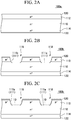
FIG. 2 is a view illustrating a semiconductor device manufacturing method according to the first embodiment. -
FIG. 3 is a view illustrating the semiconductor device manufacturing method according to the first embodiment. -
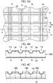
FIG. 4 is a view illustrating a semiconductor substrate cutting step according to the first embodiment. -
FIG. 5 is a view illustrating a semiconductor device manufacturing method according to a second embodiment. -
FIG. 6 is a view illustrating the semiconductor device manufacturing method according to the second embodiment. -
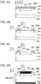
FIG. 7 is a graph showing a relationship between a depth direction from an exposed surface and an impurity concentration after a channel stopper forming step. -
FIG. 8 is a graph showing a relationship between the depth direction from the exposed surface and the impurity concentration before and after an oxide film forming step. - Hereinafter, a first embodiment of the present invention will be described with reference to
FIGS. 1 to 4 . - A semiconductor device according to the present embodiment is a mesa semiconductor device provided with a channel stopper. Hereinafter, a configuration of the semiconductor device according to the present embodiment will be described with reference to
FIG. 1 . - As shown in
FIG. 1 , asemiconductor device 100 according to the present embodiment includes: asemiconductor element 100c havingfirst semiconductor layer 110 of n--type (first conductivity type) and asecond semiconductor layer 112 of p+-type (second conductivity type) disposed on one main surface side of thefirst semiconductor layer 110; achannel stopper 124; and aglass layer 128. - The
semiconductor element 100c further includes athird semiconductor layer 114 of n+-type (first conductivity type) disposed on the other main surface side of thefirst semiconductor layer 110. Thesemiconductor device 100 further includes: anoxide film 126; ananode electrode 130 formed on a surface of thesecond semiconductor layer 112; and acathode electrode 132 formed on a surface of thethird semiconductor layer 114. - The
semiconductor element 100c has an exposedsurface 111 where a pn junction formed at a junction portion between thefirst semiconductor layer 110 and thesecond semiconductor layer 112 is exposed. Thechannel stopper 124 is formed in a first exposedregion 111a of the exposedsurface 111 where thefirst semiconductor layer 110 is exposed. Theoxide film 126 is formed so as to cover the exposedsurface 111. Theglass layer 128 is formed so as to cover theoxide film 126. - As shown in
FIGS. 2 and3 , a semiconductor device manufacturing method according to the present embodiment includes the following steps in sequence. Each step will be described in sequence below. - As shown in
FIG. 2A , a semiconductor layered structure forming process is a process of forming a semiconductorlayered structure 100a that includes: afirst semiconductor layer 110 of n--type (first conductivity type); asecond semiconductor layer 112 of p+-type (second conductivity type) disposed on one main surface side of thefirst semiconductor layer 110; and athird semiconductor layer 114 of n+-type (first conductivity type) disposed on the other main surface side of thefirst semiconductor layer 110. - In the semiconductor layered structure forming process, first, the
second semiconductor layer 112 of p+-type is formed by diffusing a p-type impurity from one main surface of the silicon substrate of n--type (first semiconductor layer of n--type) 110. Additionally, thethird semiconductor layer 114 of n+-type is formed by diffusing an n-type impurity from the other main surface of thesilicon substrate 110 of n--type. Thus, the semiconductor layeredstructure 100a in which the pn junction parallel to the main surface is formed at the junction portion between thefirst semiconductor layer 110 of n--type and thesecond semiconductor layer 112 of p+-type. Thereafter, asurface oxide film 120 is formed by thermal oxidation on the surface of thesecond semiconductor layer 112 of p+-type. Additionally, asurface oxide film 122 is formed by thermal oxidation on the surface of thethird semiconductor layer 114 of n+-type. - An impurity concentration of the
first semiconductor layer 110 is, for example, 2×1014cm-3. An impurity concentration of thesecond semiconductor layer 112 is, for example, 2×1019cm-3. An impurity concentration of thethird semiconductor layer 114 is, for example, 2×1019cm-3. A thickness of thefirst semiconductor layer 110 is, for example, 150µm. A thickness of thesecond semiconductor layer 112 is, for example, 60µm. A thickness of thethird semiconductor layer 114 is, for example, 40µm. - As shown in
FIGS. 2A and 2B , a semiconductor substrate preparing step is a step of forming agroove 118 from the one main surface side of the semiconductor layeredstructure 100a and preparing asemiconductor substrate 100b having, on an inner surface of thegroove 118, the exposedsurface 111 where the pn junction formed at the junction portion between thefirst semiconductor layer 110 and thesecond semiconductor layer 112 is exposed. - The formation of the
groove 118 is performed by, for example, etching. First, thesurface oxide film 120 on thesecond semiconductor layer 112 is etched. Further, the semiconductor layeredstructure 100a is etched from thesecond semiconductor layer 112 side. As a result, thegroove 118 having a depth exceeding the pn junction is formed from the one main surface of the semiconductor layeredstructure 100a. At this time, the exposedsurface 111 is formed on the inner surface of thegroove 118. The exposedsurface 111 is composed of a first exposedregion 111a where thefirst semiconductor layer 110 is exposed and a second exposedregion 111b where thesecond semiconductor layer 112 is exposed. As an etching solution, for example, a mixed solution of hydrofluoric acid (HF), nitric acid (HNO3) and acetic acid (CH3COOH) (e.g., HF: HNO3: CH3COOH=1:4:1) is used. - A width of the
groove 118 is, for example, 300µm, while a depth of thegroove 118 is, for example, 90µm. - A pretreatment step is a step of performing a hydrophobic treatment on the first
exposed region 111a of the exposedsurface 111 where thefirst semiconductor layer 110 is exposed. - The hydrophobic treatment is performed by, for example, immersing the first
exposed region 111a into a hydrophobic treatment solution. As the hydrophobic treatment solution, for example, a mixed solution of hydrofluoric acid (HF) and nitric acid (HNO3) can be preferably used. More preferably, HF:HNO3=1:25. A time for immersing the firstexposed region 111a is preferably 1 to 3 minutes. A temperature at which the firstexposed region 111a is immersed is preferably 20 to 30°C. After the immersion, the firstexposed region 111a is cleaned with, for example, water. - As shown in
FIG. 2C , an impurity supplying step is a step of supplying animpurity 10 of n-type to the firstexposed region 111a. - The impurity supplying step is performed by, for example, applying a liquid containing the
impurity 10 of n-type (first conductivity type) onto the firstexposed region 111a. As the liquid containing theimpurity 10 of n-type, for example, a liquid obtained by dissolving a phosphorus compound (e.g., pyrophosphoric acid) in an organic solvent (e.g., ethanol), or the like, can be preferably used. As a coating method, a known method such as a dipping method, a spinner method, a spray method, or the like, can be used. - An amount of the
impurity 10 of n-type supplied to the firstexposed region 111a is adjusted so that the impurity concentration of the channel stopper 124 (seeFIG. 3A ) formed in the firstexposed region 111a in a channel stopper forming step described later becomes an optimum concentration (e.g., 1×1019cm-3). - As shown in
FIG. 3A , the channel stopper forming step is a step of introducing theimpurity 10 of n-type (first conductivity type) into thefirst semiconductor layer 110 to form thechannel stopper 124. - The introduction of the
impurity 10 of n-type is performed by, for example, irradiating thefirst exposure region 111a with a laser light. As the laser light, for example, a green laser having a wavelength of 532nm can be used. For example, the laser light is pulse-oscillated with a pulse of 30kHz and is scanned along thegroove 118 at a speed of 300mm/sec. In this step, thechannel stopper 124 is formed to a predetermined depth (first depth). - In this step, the
channel stopper 124 extending along thegroove 118 is formed. The number ofchannel stoppers 124 may be only one. In the present embodiment, the twochannel stoppers groove 118. - After the irradiation with the laser light, the remaining
impurity 10 of n-type is removed. The removal of the impurity is performed by, for example, etching. As an etching liquid, for example, the same as that used in the semiconductor substrate preparing step can be used. - As shown in
FIG. 3B , an oxide film forming step is a step of, after the channel stopper forming step and before a glass layer forming step described later, forming theoxide film 126 so as to cover the exposedsurface 111. - The formation of the
oxide film 126 is performed by, for example, a thermal oxidation method using dry oxygen. As a result, a silicon oxide film is formed on the inner surface of thegroove 118. - The formation of the
oxide film 126 is performed by, for example, placing thesemiconductor substrate 100b in a diffusion furnace and then treating it while flowing oxygen gas. A treatment temperature is preferably 900°C or higher. A treatment time is preferably 90 minutes at the treatment temperature 900°C. - A thickness of the
oxide film 126 is 5nm to 60nm, preferably 50nm. If the thickness of theoxide film 126 is less than 5nm, the reverse current reduction effect might not be obtained, which is not preferable. On the other hand, if the thickness of theoxide film 126 exceeds 60nm, it might not be able to form theglass layer 128 by electrophoresis in a glass layer forming step described later, which is not preferable. - As shown in
FIG. 3C , the glass layer forming step is a step of forming theglass layer 128 for passivation so as to cover the exposedsurface 111 using a glass composition. - In the glass layer forming step, first, a glass composition is deposited by electrophoresis on the inner surface of the
groove 118 and the surface of thesemiconductor substrate 100b in the vicinity thereof. Then, the deposited glass composition is baked. Thereby, theglass layer 128 is formed. As a result, the exposedsurface 111 on the inner surface of thegroove 118 is covered with theglass layer 128 via theoxide film 126. - A baking temperature of the glass composition is, for example, 900°C. Additionally, a baking time of the glass composition is, for example, 15 to 30 minutes at the baking temperature 900°C.
- As the glass composition, it is possible to use, for example, a glass composition containing at least two alkaline earth metal oxides of SiO2, Al2O3, B2O3, ZnO, CaO, BaO and MgO, and substantially not containing Pb, As, Sb, Li, Na, and K.
- As the glass composition, it is preferable to use a glass composition satisfying that the amount of SiO2 is within the range of 49.5mol% to 64.3mol%, the amount of Al2O3 is within the range of 3.7mol% to 14.8mol%, the amount of B2O3 is within the range of 8.4mol% to 17.9mol%, the amount of ZnO is within the range of 3.9mol% to 14.2mol%, the amount of the alkaline earth metal oxide is within the range of 7.4mol% to 12.9mol%.
- Here, in this case, "to contain a specific component" includes not only a case where it contains only the specific component, but also a case where it further contains, in addition to the certain component, a component normally containable in the glass composition. Additionally, "substantially does not contain a specific element" means that the specific element is not contained as a component, and it does not exclude a glass composition in which the above specific element is mixed as an impurity in the raw material of each component constituting the glass. Further, "not containing a specific element" means that it does not contain an oxide of the specific element, a nitride of the specific element, or the like.
- The reason that the amount of SiO2 is set within the range of 49.5mol% to 64.3mol% is as follows. When the amount of SiO2 is less than 49.5mol%, the chemical resistance of the
glass layer 128 might be lowered, or the insulating property of theglass layer 128 might be deteriorated. When the amount of SiO2 exceeds 64.3mol%, the baking temperature of the glass composition might increase. - The reason that the amount of Al2O3 is set within the range of 3.7mol% to 14.8mol% is as follows. When the amount of Al2O3 is less than 3.7mol%, the chemical resistance of the
glass layer 128 might be lowered, or the insulating property of theglass layer 128 might be deteriorated. When the amount of Al2O3 exceeds 14.8mol%, the baking temperature of the glass composition might increase. - The reason that the amount of B2O3 is set within the range of 8.4mol% to 17.9mol% is as follows. When the amount of B2O3 is less than 8.4mol%, the baking temperature of the glass composition might increase. When the amount of B2O3 exceeds 17.9mol%, B (boron) diffuses into the
semiconductor substrate 100b during the baking of the glass composition, and the insulating property might be deteriorated. - The reason that the amount of ZnO is set within the range of 3.9mol% to 14.2mol% is as follows. When the amount of ZnO is less than 3.9mol%, the baking temperature of the glass composition might increase. When the amount of ZnO exceeds 14.2mol%, the chemical resistance of the
glass layer 128 might be lowered, or the insulating property of theglass layer 128 might be deteriorated. - Additionally, the reason that the amount of the alkaline earth metal oxide is set within the range of 7.4mol% to 12.9mol% is as follows. When the amount of the alkaline earth metal oxide is less than 7.4mol%, the baking temperature of the glass composition might increase. When the amount of the alkaline earth metal oxide exceeds 12.9mol%, the chemical resistance of the
glass layer 128 might be lowered, or the insulating property of theglass layer 128 might be deteriorated. - As the glass composition, it is preferable to use one having an average coefficient of linear expansion that is within the range of 3.33×10⁻⁶ to 4.13×10⁻⁶ at the temperature range of 50°C to 550°C.
- The glass composition according to the present embodiment can be formed, for example, as follows. First, raw materials (SiO2, Al(OH)3, H3BO3, ZnO, CaCO3, Mg(OH)2, BaO) are compounded so as to have the above composition ratio (molar ratio). Next, the raw materials are thoroughly stirred with a mixer. Next, the stirred raw materials are placed in a platinum crucible which has been raised to a predetermined temperature (e.g., 1550°C) in an electric furnace, and are melted for a predetermined time (e.g., 30 to 120 minutes). Next, the melt of the raw materials is poured into a water cooling roll. Thus, flaky glass flakes are obtained. Finally, the glass flakes are pulverized to a predetermined average particle size with a ball mill or the like. Thereby, a powdery glass composition is obtained.
- The electrode forming step is a step of forming an
anode electrode 130 and a cathode electrode 132 (seeFIG. 4B ) on thesemiconductor substrate 100b. - In the electrode forming step, first, a photoresist is formed so as to cover the surface of the
glass layer 128. Next, a portion of the one main surface of thesemiconductor substrate 100b where theanode electrode 130 is not to be formed is masked with the photoresist. Next, thesurface oxide film 120 is etched. As a result, thesurface oxide film 120 is removed from the portion of the one main surface of thesemiconductor substrate 100b where theanode electrode 130 is to be formed. Additionally, thesurface oxide film 122 is removed from on the other main surface of thesemiconductor substrate 100b. Next, a plating process is performed on thesemiconductor substrate 100b. As a result, theanode electrode 130 is formed on the portion of the one main surface of thesemiconductor substrate 100b from which thesurface oxide film 120 has been removed. Additionally, thecathode electrode 132 is formed on the other main surface of thesemiconductor substrate 100b. - As shown in
FIG. 4 , a semiconductor substrate cutting step is a step of cutting thesemiconductor substrate 100b into chips to manufacture thesemiconductor device 100.FIG. 4B is a cross section taken along a line A-A inFIG. 4A . - In the semiconductor substrate cutting step, as shown in
FIGS. 4A and 4B , thesemiconductor substrate 100b is cut using, for example, a dicing saw, along dicing lines DL each passing through the center, in the width direction, of thegroove 118. As a result, as shown inFIG. 4C , thesemiconductor substrate 100b is formed into chips, so that thesemiconductor device 100 which is a mesa-type pn diode is manufactured. - As described above, according to the semiconductor device manufacturing method of the present embodiment, the hydrophobic treatment is performed in the pretreatment step, thereby making it possible to increase the concentration of the
impurity 10 of the first conductivity type introduced into thefirst semiconductor layer 110 by the irradiation of the laser light in the channel stopper forming step. This point will be described with reference toFIG. 7 . - A practical example shown in
FIG. 7 is a result when the following processing was performed. First, in the pretreatment step of the present embodiment, a hydrophobic treatment was performed using a mixed solution of hydrofluoric acid and nitric acid (HF:HNO3=1:25). Next, in the impurity supplying step, a liquid in which pyrophosphoric acid was dissolved in ethanol was applied by a dipping method. Next, in the channel stopper forming step, a green laser with a wavelength of 532nm was irradiated while pulsing with a pulse of 30kHz. - A comparative example is a result of having performed, in the pretreatment step of the present embodiment, the impurity supplying step and the channel stopper forming step without performing the hydrophobic treatment, under the same conditions as in the practical example.
- In the practical example, the concentration of the
impurity 10 becomes higher than that in the comparative example, regardless of the depth (position) from the exposedsurface 111. For example, the peak of the concentration of theimpurity 10 in the vicinity of the exposedsurface 111 is about 1019/cm3 in the comparative example, while it is about 1020/cm3 in the practical example. Therefore, in order to raise the concentration of the channel stopper, it is effective to perform the hydrophobic treatment in the pretreatment step. - Since the concentration of the
impurity 10 can be increased as described above, spreading of the depletion layer can be suppressed at the time of application of the reverse bias voltage even in a higher temperature environment, so that generation of leakage current can be suppressed. Therefore, thesemiconductor device 100 can be normally operated. In other words, a highlyreliable semiconductor device 100 can be provided. - Additionally, according to the semiconductor device manufacturing method of the present embodiment, in the glass layer forming step, the
glass layer 128 is formed by baking the layer made of the glass composition formed so as to cover the exposedsurface 111. Thereby, theimpurity 10 of the first conductivity type introduced into the firstexposed region 111a of the exposedsurface 111 can be diffused in thefirst semiconductor layer 110 by the heat applied in the baking. This makes it possible to further suppress the spreading of the depletion layer at the time of application of the reverse bias voltage. As a result, the generation of leakage current can be further suppressed. Therefore, asemiconductor device 100 with higher reliability can be provided. - Further, according to the semiconductor device manufacturing method of the present embodiment, after the channel stopper forming step and before the glass layer forming step, in the oxide film forming step, the
oxide film 126 is formed so as to cover the exposedsurface 111. As a result, theimpurity 10 of the first conductivity type introduced into the firstexposed region 111a of the exposedsurface 111 can be diffused in thefirst semiconductor layer 110 by the heat applied in the formation of theoxide film 126. This point will be described with reference toFIG. 8 . - As shown in
FIG. 8 , after the oxide film forming step, theimpurity 10 thermally diffuse from the exposedsurface 111 to a deeper position than before the oxide film forming step. As a result, the height of the peak of the concentration of theimpurity 10 in the vicinity of the exposedsurface 111 decreases through the oxide film forming step, whereas the width of the peak spreads from the exposedsurface 111 to a deeper position. In other words, in the oxide film forming step, the region of thechannel stopper 124 is enlarged to a second depth deeper than the first depth that is after the channel stopper forming step. - This makes it possible to suppress the spreading of the depletion layer at the time of application of the reverse bias voltage. As a result, the generation of leakage current can be suppressed. Therefore, a
semiconductor device 100 with higher reliability can be provided. - Additionally, according to the semiconductor device manufacturing method of the present embodiment, it is possible to introduce the impurity deeper without increasing the power of the laser. This makes it possible to suppress generation of surface defects based on the laser irradiation. Therefore, in the manufactured
semiconductor device 100, occurrence of leakage current can be suppressed. - Further, according to the semiconductor device manufacturing method of the present embodiment, the glass composition as the raw material of the
glass layer 128 does not substantially contain Pb, As, and Sb, which are environmentally harmful substances. Thereby, the environmental burden can be reduced. Moreover, theglass layer 128 is made of lead-free glass having a dielectric constant lower than that of the lead-containing glass. Thereby, even when a reverse bias voltage is applied in a high-temperature environment to a resin-molded semiconductor device in which thesemiconductor device 100 is molded with resin, high density ions are suppressed from being induced into an interface between the mold resin and theglass layer 128 and an interface between theglass layer 128 and thefirst semiconductor layer 110. As a result, the high-temperature reverse bias withstand capability can be made higher than that of a resin-sealed semiconductor device obtained by molding with a resin a semiconductor device obtained using a conventional lead-containing glass. - Moreover, according to the semiconductor device manufacturing method of the present embodiment, the glass composition as the raw material of the
glass layer 128 does not substantially contain Li, Na, and K. Thereby, even if B (boron) is contained in the glass composition, B (boron) does not diffuse into silicon from theglass layer 128 during the baking of the glass composition. Thereby, a highlyreliable semiconductor device 100 can be provided. - Additionally, according to the semiconductor device manufacturing method of the present embodiment, since the
glass layer 128 is formed by baking the layer made of the glass composition for protecting the semiconductor junction including glass fine particles prepared from the melt obtained by melting raw materials containing at least two alkaline earth metal oxides of SiO2, Al2O3, B2O3, ZnO, CaO, MgO, and BaO, but substantially not containing Pb, As, Sb, Li, Na and K, it is possible to bake the glass composition at a relatively low temperature. This makes it difficult for the glass composition to crystallize during the baking process of the glass composition. As a result, it is possible to stably manufacture asemiconductor device 100 having a low reverse leakage current. - Further, according to the semiconductor device manufacturing method of the present embodiment, the glass composition satisfies that the amount of SiO2 is within the range of 49.5mol% to 64.3mol%, the amount of Al2O3 is 3.7mol% to 14.8mol%, the amount of B2O3 is within the range of 8.4mol% to 17.9mol%, the amount of ZnO is within the range of 3.9mol% to 14.2mol%, and the amount of the alkaline earth metal oxide is within the range of 7.4mol% to 12.9mol%. Thereby, it is possible to suppress the increase in baking temperature of the glass composition, the deterioration of the chemical resistance of the
glass layer 128, and the deterioration of the insulation property of theglass layer 128. - Moreover, according to the semiconductor device manufacturing method of the present embodiment, the average coefficient of linear expansion of the glass composition within the temperature range of 50°C to 550°C is within the range of 3.33×10⁻⁶ to 4.08×10⁻⁶. As a result, since the glass composition has a coefficient of linear expansion close to that of silicon, it is possible to prevent the
semiconductor substrate 100b from warping during the manufacturing process. - Additionally, according to the semiconductor device manufacturing method of the present embodiment, the exposed
surface 111 is the inner surface of thegroove 118 formed so as to separate thesecond semiconductor layer 112 into a mesa shape and to reach thefirst semiconductor layer 110. This makes it possible to provide thechannel stopper 124 on the bottom surface of thegroove 118 in themesa semiconductor device 100. As a result, even when the depletion layer of the pn junction spreads at a high voltage, the depletion layer is terminated by thechannel stopper 124 and will not be exposed to the chip-section cross section. Therefore, it is possible to increase the withstand voltage of themesa semiconductor device 100. - Further, according to the semiconductor device manufacturing method of the present embodiment, the mixed solution of hydrofluoric acid (HF) and nitric acid (HNO3) is used in the hydrophobic treatment in the pretreatment step. This makes it possible to perform the hydrophobic treatment using chemicals commonly used in ordinary semiconductor processes.
- Hereinafter, a second embodiment of the present invention will be described. A semiconductor device according to the present embodiment is a planar semiconductor device provided with a channel stopper. Hereinafter, a configuration of the semiconductor device according to the present embodiment will be described with reference to
FIG. 6D . - As shown in
FIG. 6D , a semiconductor device 200 according to the present embodiment includes: asemiconductor element 200c having afirst semiconductor layer 210 of n--type (first conductivity type) and asecond semiconductor layer 212 of p+-type (second conductivity type) disposed on one main surface side of thefirst semiconductor layer 210; achannel stopper 224; and aglass layer 228. - The
semiconductor element 200c further includes athird semiconductor layer 214 of n+-type (first conductivity type) disposed on the other main surface side of thefirst semiconductor layer 210. The semiconductor device 200 further includes: anoxide film 226; ananode electrode 230 formed on a surface of thesecond semiconductor layer 212; and acathode electrode 232 formed on a surface of thethird semiconductor layer 214. - The
semiconductor element 200c has an exposedsurface 211 where a pn junction formed at a junction portion between thefirst semiconductor layer 210 and thesecond semiconductor layer 112 is exposed. Thechannel stopper 224 is formed in the firstexposed region 211a of the exposedsurface 211 where thefirst semiconductor layer 210 is exposed. Theoxide film 226 is formed so as to cover the exposedsurface 211. Theglass layer 228 is formed so as to cover theoxide film 226. - As shown in
FIGS. 5 and6 , the semiconductor device manufacturing method of the present embodiment includes the following steps in sequence. Each step will be described in sequence below. - As shown in
FIGS. 5A to 5C , a semiconductor layered structure forming process is a process of forming a semiconductor layeredstructure 200a that includes: afirst semiconductor layer 210 of n--type (first conductivity type); asecond semiconductor layer 212 of p+-type (second conductivity type) disposed on one main surface side of thefirst semiconductor layer 210; and athird semiconductor layer 214 of n+-type (first conductivity type) disposed on the other main surface side of thefirst semiconductor layer 110. - In the semiconductor substrate preparing step, for example, first, as shown in
FIG. 5A , anepitaxial layer 210 of n--type is layered on thesemiconductor substrate 214 of n+-type. Next, as shown inFIG. 5B , after a mask M1 is formed, an impurity of p-type (e.g., B (Boron) ion) is introduced by ion implantation into a predetermined region of a surface of theepitaxial layer 210 of n--type through the mask M1. The mask M1 is provided so that a part of the one main surface of thesemiconductor substrate 200a is opened. Next, adiffusion layer 212 of p+-type is formed by thermal diffusion. Next, the mask M 1 is removed. Thereby, thesemiconductor base 200a is prepared. At this time, the exposedsurface 211 is formed on the one main surface of thesemiconductor substrate 200a. The exposedsurface 211 is composed of a firstexposed region 211a where thefirst semiconductor layer 210 is exposed and a secondexposed region 211b where thesecond semiconductor layer 212 is exposed. - A pretreatment step is a step of performing hydrophobic treatment on the first
exposed region 211 a of the exposedsurface 211 where thefirst semiconductor layer 210 is exposed. - The hydrophobic treatment is performed by, for example, immersing the first
exposed region 211a into a hydrophobic treatment solution. As the hydrophobic treatment solution, as in the first embodiment, a mixed solution of hydrofluoric acid (HF) and nitric acid (HNO3) can be preferably used. - As shown in
FIG. 5C , an impurity supplying step is a step of supplying animpurity 20 of n-type to the firstexposed region 211a. - For example, the impurity supplying step is performed by, for example, applying a liquid containing an
impurity 20 of n-type (first conductivity type) to thefirst exposure region 211a. As the liquid containing the n-type impurity 20, a liquid obtained by dissolving a phosphorus compound in an organic solvent or the like can be preferably used as in the first embodiment. As a coating method, as in the first embodiment, a known method such as a dipping method, a spinner method, a spray method, or the like can be used. - As shown in
FIG. 5D , a channel stopper forming step is a step of introducing animpurity 20 of n-type (first conductivity type) into thefirst semiconductor layer 210 to form achannel stopper 224. - As in the first embodiment, the introduction of the
impurity 10 of n-type is performed by irradiating a predetermined region of thefirst exposure region 211a with laser light. - As shown in
FIG. 5E , an oxide film forming step is a step of, after the channel stopper forming step and before the glass layer forming step described later, forming anoxide film 226 so as to cover the exposedsurface 211. - The formation of the oxide film is performed by, for example, a thermal oxidation method using dry oxygen, as in the first embodiment. As a result, the
oxide film 226 is formed on the one main surface of thesemiconductor substrate 200a. At this time, asurface oxide film 222 is also formed on the other main surface of thesemiconductor substrate 200a. - As shown in
FIG. 6A , a glass layer forming step is a step of forming aglass layer 228 for passivation so as to cover the exposedsurface 211 using a glass composition. - In the glass layer forming step, as in the first embodiment, a glass composition is deposited by electrophoresis on the one main surface side of the
semiconductor substrate 200a. Then, the deposited glass composition is baked. As a result, the exposedsurface 211 is covered with theglass layer 228 via thesurface oxide film 226. - As the glass composition, one having the same composition as that of the first embodiment can be preferably used. As the glass composition, one having the same coefficient of linear expansion as that of the first embodiment can be preferably used.
- As shown in
FIGS. 6B and 6C , an etching step is a step of forming theoxide film 226 and theglass layer 228 on a predetermined region of the one main surface of thesemiconductor substrate 200a. - In the etching step, for example, a mask M2 is formed on the one main surface side of the
semiconductor substrate 200a so as to cover a boundary between thefirst exposure region 211a and thesecond exposure region 211b. Next, theglass layer 228 and theoxide film 226 are etched. Thus, theoxide film 226 and theglass layer 228 can be formed only in the predetermined region. At this time, theoxide film 222 is removed from the other main surface of thesemiconductor substrate 200a. - As shown in
FIG. 6D , the electrode forming step is a step of forming ananode electrode 230 and acathode electrode 232 on thesemiconductor substrate 200a. - In the electrode forming step, after the mask M2 is removed, the
anode electrode 230 is formed in a region of the one main surface of thesemiconductor substrate 200a, which is surrounded by theglass layer 228. Additionally, thecathode electrode 232 is formed on the rear surface of thesemiconductor substrate 200a. - As in the first embodiment, a semiconductor substrate cutting step is a process of cutting the
semiconductor substrate 200a into chips using a dicing saw or the like. As a result, as shown inFIG. 6D , thesemiconductor substrate 200a is formed into a chip, and the semiconductor device 200 which is a planar type pn diode is manufactured. - As described above, according to the semiconductor device manufacturing method of the present embodiment, the same effects as those of the first embodiment are achieved. In other words, by performing the hydrophobic treatment in the pretreatment step, it is possible to increase the concentration of the
impurity 20 of the first conductivity type introduced into thefirst semiconductor layer 210 by the irradiation of laser light in the channel stopper formation step. As a result, even in a higher temperature environment, spreading of the depletion layer can be suppressed at the time of application of the reverse bias voltage, so that occurrence of leakage current can be suppressed. Therefore, it is possible to operate the semiconductor device normally. In other words, a highly reliable semiconductor device 200 can be provided. - Additionally, according to the semiconductor device manufacturing method of the present embodiment, in the glass layer forming step, the
glass layer 228 is formed by baking the layer made of the glass composition formed so as to cover the exposedsurface 211. Therefore, theimpurity 20 of the first conductivity type introduced into the firstexposed region 211 a of the exposedsurface 211 can be diffused in thefirst semiconductor layer 210 by the heat applied in the baking. This makes it possible to further suppress the spreading of the depletion layer at the time of application of the reverse bias voltage. As a result, generation of leakage current can be further suppressed, and a semiconductor device 200 with higher reliability can be provided. - Further, according to the semiconductor device manufacturing method of the present embodiment, after the channel stopper forming step and before the glass layer forming step, the
oxide film 226 is formed so as to cover the exposedsurface 211 in the oxide film forming step. As a result, theimpurity 20 of the first conductivity type introduced into the firstexposed region 211a of the exposedsurface 211 can be diffused in thefirst semiconductor layer 210 by the heat applied in forming theoxide film 226. This makes it possible to further suppress the spreading of the depletion layer at the time of application of the reverse bias voltage, so that it is possible to further suppress the occurrence of the leakage current. Therefore, a semiconductor device 200 with higher reliability can be provided. - Moreover, according to the semiconductor device manufacturing method according to the present embodiment, the glass composition as the raw material of the
glass layer 228 does not substantially contain Pb, As, and Sb, which are environmentally harmful substances. Thereby, the environmental burden can be reduced. Further, theglass layer 228 is made of lead-free glass having a dielectric constant lower than that of the lead-containing glass. As a result, even when a reverse bias voltage is applied in a high-temperature environment to a resin-molded semiconductor device obtained by molding the semiconductor device 200 with a resin, high density ions are suppressed from being induced to an interface between the mold resin and theglass layer 228 and an interface between theglass layer 228 and thefirst semiconductor layer 210. As a result, the high-temperature reverse bias withstand capability can be made higher than that of a resin-sealed semiconductor device obtained by molding with a resin a semiconductor device obtained by using a conventional lead-containing glass. - Additionally, according to the semiconductor device manufacturing method of the present embodiment, the glass composition as the raw material of the
glass layer 228 does not substantially contain Li, Na, and K. Thereby, even if B (boron) is contained in the glass composition, B (boron) does not diffuse into silicon from the glass layer during the baking of the glass composition. Thereby, a highly reliable semiconductor device 200 can be provided. - Further, according to the semiconductor device manufacturing method of the present embodiment, since the
glass layer 228 is formed by baking the layer made of the glass composition for protecting the semiconductor junction including glass fine particles prepared from the melt obtained by melting raw materials containing at least two alkaline earth metal oxides of SiO2, Al2O3, B2O3, ZnO, CaO, MgO, and BaO, but substantially not containing Pb, As, Sb, Li, Na and K, it is possible to bake the glass composition at a relatively low temperature. This makes it difficult for the glass composition to crystallize during the baking process of the glass composition. As a result, it is possible to stably manufacture a semiconductor device 200 having a low reverse leakage current. - Moreover, according to the semiconductor device manufacturing method of the present embodiment, the glass composition satisfies that the amount of SiO2 is within the range of 49.5mol% to 64.3mol%, the amount of Al2O3 is within the range of 3.7mol% to 14.8mol%, the amount of B2O3 is within the range of 8.4mol% to 17.9mol%, the amount of ZnO is within the range of 3.9mol% to 14.2mol%, and the amount of the alkaline earth metal oxide is within the range of 7.4mol% to 12.9mol%. Thereby, it is possible to suppress the increase in baking temperature of the glass composition, the deterioration of the chemical resistance of the
glass layer 228, and the deterioration of the insulation property of theglass layer 128. - Additionally, according to the semiconductor device manufacturing method of the present embodiment, the average coefficient of linear expansion of the glass composition within the temperature range of 50°C to 550°C is within the range of 3.33×10⁻⁶ to 4.08×10⁻⁶. As a result, since the glass composition has a coefficient of linear expansion close to that of silicon, it is possible to prevent the
semiconductor substrate 200a from warping during the manufacturing process. - Further, according to the semiconductor device manufacturing method of the present embodiment, the mixed solution of hydrofluoric acid (HF) and nitric acid (HNO3) is used in the hydrophobic treatment in the pretreatment step. This makes it possible to perform the hydrophobic treatment using chemicals commonly used in ordinary semiconductor processes.
- Although the preferred embodiments of the present invention have been described above with reference to the accompanying drawings, it is needless to say that the present invention is not limited to such examples. The shapes and combinations of the constituent members shown in the above examples are merely examples, and various modifications can be made based on design requirements or the like without departing from the gist of the present invention.
- In the semiconductor device manufacturing method of the present invention, the oxide film forming step may not be performed.
- The semiconductor device manufacturing method of the present invention may include at least the semiconductor substrate preparing step, the pretreatment step, the impurity supplying step, the channel stopper forming step, and the glass film forming step.
- The semiconductor device of the present invention may include at least the semiconductor element, the channel stopper, and the glass layer.
- Although the description has been given in the above embodiments assuming that the first conductivity type is n-type while the second conductivity type is p-type, the present invention is not limited thereto, and the first conductivity type may be p-type while the second conductivity type may be n-type.
- In the above embodiment, a grain laser is used as a laser, but the present invention is not limited thereto. As the laser, a visible light laser other than the green laser, or a near infrared light laser (e.g., Nd-YAG laser) can also be preferably used.
- In the above embodiment, although the liquid in which pyrophosphoric acid is dissolved in the organic solvent is used as the liquid containing the impurity of n-type, the present invention is not limited thereto. For example, it is possible to use a liquid in which a phosphorus compound other than pyrophosphoric acid or an arsenic compound is dissolved in various organic solvents.
- In the above embodiment, the present invention has been described by exemplifying the pn diode as the semiconductor device, but the present invention is not limited thereto. For example, it is possible to apply the present invention to a diode other than a pn diode (e.g., a pin diode, a Schottky diode, etc.), a transistor (e.g., a bipolar transistor, a MOSFET, an IGBT, etc.), a thyristor, a triac, and other power semiconductor devices.
- 10, 20 ... impurity of n-type (first conductivity type), 100 ... semiconductor device, 100a ... semiconductor layered structure, 100b, 200a ... semiconductor substrate, 100c ... semiconductor element, 110, 210 ... first semiconductor layer, 111, 211 ... exposed surface, 111a, 211a ... first exposed region, 111b, 211b ... second exposed region, 112, 212 ... second semiconductor layer, 114, 214 ... third semiconductor layer, 120, 122, 222 ... surface oxide film, 124, 224 ... channel stopper, 126, 226 ... oxide film, 128, 228 ... glass layer, 130, 230 ... anode electrode, 132, 232 ... cathode electrode
Claims (11)
- A semiconductor device manufacturing method comprising:a semiconductor substrate preparing step of preparing a semiconductor substrate having an exposed surface where a pn junction is exposed, the pn junction being formed at a junction portion between a first semiconductor layer of a first conductivity type and a second semiconductor layer of a second conductivity type opposite to the first conductivity type;a pretreatment step of performing a hydrophobic treatment on a first exposed region of the exposed surface where the first semiconductor layer is exposed;an impurity supplying step of supplying an impurity of the first conductivity type to the first exposed region;a channel stopper forming step of irradiating the first exposed region with a laser beam to introduce the impurity of the first conductivity type into the first semiconductor layer, thus forming a channel stopper; anda glass layer forming step of forming a glass layer using a glass composition so as to cover the exposed surface.
- The semiconductor device manufacturing method according to claim 1, wherein
in the glass layer forming step, a layer made of the glass composition is formed so as to cover the exposed surface, and then the layer made of the glass composition is baked to form the glass layer - The semiconductor device manufacturing method according to claim 1 or 2, further comprising:an oxide film forming step of forming an oxide film so as to cover the exposed surface after the channel stopper forming step and before the glass layer forming step.
- The semiconductor device manufacturing method according to any one of claims 1 to 3, wherein
the glass composition substantially does not contain Pb. - The semiconductor device manufacturing method according to any one of claims 1 to 4, wherein
the glass composition substantially does not contain As, Sb, Li, Na, and K. - The semiconductor device manufacturing method according to any one of claims 1 to 3, wherein
the glass composition contains at least two alkaline earth metal oxides of SiO2, B2O3, Al2O3, ZnO, CaO, MgO, and BaO, and substantially does not contain Pb, As, Sb, Li, Na, and K. - The semiconductor device manufacturing method according to claim 6, wherein
the glass composition satisfies that
an amount of SiO2 is within a range of 49.5mol% to 64.3mol%,
an amount of Al2O3 is within a range of 3.7mol% to 14.8mol%,
an amount of B2O3 is within a range of 8.4mol% to 17.9mol%,
an amount of ZnO is within a range of 3.9mol% to 14.2mol%, and
an amount of the alkaline earth metal oxide is within a range of 7.4mol% to 12.9mol%. - The semiconductor device manufacturing method according to any one of claims 1 to 7, wherein
an average linear expansion coefficient of the glass composition within a temperature range of 50°C to 550°C is within a range of 3.33×10⁻⁶ to 4.08×10⁻⁶. - The semiconductor device manufacturing method according to any one of claims 1 to 8, wherein
the exposed surface is an inner surface of a groove formed so as to divide the second semiconductor layer into a mesa shape and to reach the first semiconductor layer. - The semiconductor device manufacturing method according to any one of claims 1 to 9, wherein
in the hydrophobic treatment, a mixed solution of HF and HNO3 is used. - A semiconductor device manufactured by the semiconductor device manufacturing method according to any one of claims 1 to 10, the semiconductor device comprising:a semiconductor element having the exposed surface;the channel stopper formed in the first exposed region of the semiconductor element; andthe glass layer formed so as to cover the exposed surface of the semiconductor element.
Applications Claiming Priority (1)
| Application Number | Priority Date | Filing Date | Title |
|---|---|---|---|
| PCT/JP2016/084913 WO2018096642A1 (en) | 2016-11-25 | 2016-11-25 | Semiconductor device production method, and semiconductor device |
Publications (3)
| Publication Number | Publication Date |
|---|---|
| EP3349239A1 true EP3349239A1 (en) | 2018-07-18 |
| EP3349239A4 EP3349239A4 (en) | 2019-06-12 |
| EP3349239B1 EP3349239B1 (en) | 2020-04-08 |
Family
ID=61628711
Family Applications (1)
| Application Number | Title | Priority Date | Filing Date |
|---|---|---|---|
| EP16909740.9A Active EP3349239B1 (en) | 2016-11-25 | 2016-11-25 | Semiconductor device production method |
Country Status (6)
| Country | Link |
|---|---|
| US (1) | US10707302B2 (en) |
| EP (1) | EP3349239B1 (en) |
| JP (1) | JP6295378B1 (en) |
| CN (1) | CN108604550B (en) |
| TW (1) | TWI652740B (en) |
| WO (1) | WO2018096642A1 (en) |
Cited By (1)
| Publication number | Priority date | Publication date | Assignee | Title |
|---|---|---|---|---|
| FR3145646A1 (en) * | 2023-02-08 | 2024-08-09 | Stmicroelectronics International N.V. | Formation of a power electronic component |
Families Citing this family (5)
| Publication number | Priority date | Publication date | Assignee | Title |
|---|---|---|---|---|
| WO2019239448A1 (en) * | 2018-06-11 | 2019-12-19 | 新電元工業株式会社 | Semiconductor device manufacturing method and semiconductor device |
| CN109755209A (en) * | 2019-01-11 | 2019-05-14 | 常州星海电子股份有限公司 | A kind of high reliability photoresist glass passivation chip and its processing method |
| CN113921588A (en) * | 2021-09-01 | 2022-01-11 | 格力电器(合肥)有限公司 | Semiconductor device and method for manufacturing the same |
| CN116565016A (en) * | 2022-01-27 | 2023-08-08 | 达尔科技股份有限公司 | Semiconductor structure and manufacturing method thereof |
| CN115241060B (en) * | 2022-06-30 | 2024-06-14 | 常州银河电器有限公司 | A new high-voltage glass protection chip manufacturing process |
Family Cites Families (12)
| Publication number | Priority date | Publication date | Assignee | Title |
|---|---|---|---|---|
| JPS55133569A (en) * | 1979-04-06 | 1980-10-17 | Hitachi Ltd | Semiconductor device |
| JPS5773956A (en) * | 1980-10-27 | 1982-05-08 | Hitachi Ltd | Glass coated semiconductor device |
| US4666557A (en) * | 1984-12-10 | 1987-05-19 | Ncr Corporation | Method for forming channel stops in vertical semiconductor surfaces |
| JPH09331049A (en) * | 1996-04-08 | 1997-12-22 | Canon Inc | Method for manufacturing bonded SOI substrate and SOI substrate |
| JPH1012897A (en) * | 1996-06-21 | 1998-01-16 | Hitachi Ltd | Glass-coated semiconductor device and method of manufacturing the same |
| JP4901300B2 (en) * | 2006-05-19 | 2012-03-21 | 新電元工業株式会社 | Manufacturing method of semiconductor device |
| JP2008072049A (en) * | 2006-09-15 | 2008-03-27 | Sumco Corp | Method for manufacturing bonded wafer |
| US8053867B2 (en) * | 2008-08-20 | 2011-11-08 | Honeywell International Inc. | Phosphorous-comprising dopants and methods for forming phosphorous-doped regions in semiconductor substrates using phosphorous-comprising dopants |
| JP5350757B2 (en) * | 2008-11-14 | 2013-11-27 | 新電元工業株式会社 | Mesa Zener Diode and Method for Manufacturing the Same |
| CN102157585B (en) * | 2011-02-28 | 2013-01-23 | 中山大学 | Method for manufacturing uniform shallow emitter solar cell |
| WO2013168314A1 (en) | 2012-05-08 | 2013-11-14 | 新電元工業株式会社 | Semiconductor device production method and semiconductor device |
| FR2982134B1 (en) * | 2011-11-07 | 2013-11-15 | Renault Sas | TOUCH TABLET SUPPORT |
-
2016
- 2016-11-25 WO PCT/JP2016/084913 patent/WO2018096642A1/en not_active Ceased
- 2016-11-25 CN CN201680043423.9A patent/CN108604550B/en active Active
- 2016-11-25 JP JP2017523553A patent/JP6295378B1/en active Active
- 2016-11-25 US US15/745,828 patent/US10707302B2/en active Active
- 2016-11-25 EP EP16909740.9A patent/EP3349239B1/en active Active
-
2017
- 2017-11-20 TW TW106140126A patent/TWI652740B/en active
Cited By (2)
| Publication number | Priority date | Publication date | Assignee | Title |
|---|---|---|---|---|
| FR3145646A1 (en) * | 2023-02-08 | 2024-08-09 | Stmicroelectronics International N.V. | Formation of a power electronic component |
| EP4415037A1 (en) * | 2023-02-08 | 2024-08-14 | STMicroelectronics International N.V. | Forming a power electronic component |
Also Published As
| Publication number | Publication date |
|---|---|
| US10707302B2 (en) | 2020-07-07 |
| EP3349239A4 (en) | 2019-06-12 |
| CN108604550A (en) | 2018-09-28 |
| US20200083321A1 (en) | 2020-03-12 |
| JPWO2018096642A1 (en) | 2018-11-22 |
| EP3349239B1 (en) | 2020-04-08 |
| JP6295378B1 (en) | 2018-03-14 |
| WO2018096642A1 (en) | 2018-05-31 |
| TW201834076A (en) | 2018-09-16 |
| TWI652740B (en) | 2019-03-01 |
| CN108604550B (en) | 2021-08-31 |
Similar Documents
| Publication | Publication Date | Title |
|---|---|---|
| EP3349239B1 (en) | Semiconductor device production method | |
| EP2858098B1 (en) | Method of manufacturing a resin-sealed semiconductor device | |
| US9941112B2 (en) | Method of manufacturing semiconductor device and semiconductor device | |
| EP2983197B1 (en) | Glass composition for protecting semiconductor junction, method of manufacturing semiconductor device and semiconductor device | |
| KR101851884B1 (en) | Manufacturing method of semiconductor device and glass coating film forming apparatus | |
| JP5340511B1 (en) | Semiconductor device manufacturing method and semiconductor device | |
| EP2849213A1 (en) | Glass composition for semiconductor junction protection, method for manufacturing semiconductor device, and semiconductor device | |
| US20130154064A1 (en) | Glass composition for protecting semiconductor junction, method of manufacturing semiconductor device and semiconductor device | |
| CN1227743C (en) | Semiconductor device and its producing method | |
| US10186425B2 (en) | Method of manufacturing semiconductor device and resist glass | |
| TWI650818B (en) | Semiconductor device manufacturing method and semiconductor device | |
| US10050133B2 (en) | Application of thin insulating film layer in semiconductor device and method of manufacturing semiconductor device | |
| KR100962832B1 (en) | Method for manufacturing semiconductor device | |
| WO2012160962A1 (en) | Semiconductor device production method and semiconductor device | |
| JP2001110799A (en) | Semiconductor element and manufacturing method therefor | |
| JP5655140B2 (en) | Semiconductor device manufacturing method and semiconductor device | |
| JP5655139B2 (en) | Semiconductor device manufacturing method and semiconductor device | |
| JPWO2013168521A1 (en) | Resin-sealed semiconductor device and manufacturing method thereof |
Legal Events
| Date | Code | Title | Description |
|---|---|---|---|
| STAA | Information on the status of an ep patent application or granted ep patent |
Free format text: STATUS: UNKNOWN |
|
| STAA | Information on the status of an ep patent application or granted ep patent |
Free format text: STATUS: THE INTERNATIONAL PUBLICATION HAS BEEN MADE |
|
| PUAI | Public reference made under article 153(3) epc to a published international application that has entered the european phase |
Free format text: ORIGINAL CODE: 0009012 |
|
| STAA | Information on the status of an ep patent application or granted ep patent |
Free format text: STATUS: REQUEST FOR EXAMINATION WAS MADE |
|
| 17P | Request for examination filed |
Effective date: 20180129 |
|
| AK | Designated contracting states |
Kind code of ref document: A1 Designated state(s): AL AT BE BG CH CY CZ DE DK EE ES FI FR GB GR HR HU IE IS IT LI LT LU LV MC MK MT NL NO PL PT RO RS SE SI SK SM TR |
|
| AX | Request for extension of the european patent |
Extension state: BA ME |
|
| RIN1 | Information on inventor provided before grant (corrected) |
Inventor name: OGASAWARA ATSUSHI Inventor name: HOMMA FUMIHIRO |
|
| A4 | Supplementary search report drawn up and despatched |
Effective date: 20190515 |
|
| RIC1 | Information provided on ipc code assigned before grant |
Ipc: H01L 29/06 20060101ALI20190509BHEP Ipc: H01L 21/268 20060101ALN20190509BHEP Ipc: H01L 21/288 20060101ALI20190509BHEP Ipc: H01L 21/329 20060101AFI20190509BHEP Ipc: H01L 29/861 20060101ALI20190509BHEP |
|
| GRAP | Despatch of communication of intention to grant a patent |
Free format text: ORIGINAL CODE: EPIDOSNIGR1 |
|
| STAA | Information on the status of an ep patent application or granted ep patent |
Free format text: STATUS: GRANT OF PATENT IS INTENDED |
|
| RIC1 | Information provided on ipc code assigned before grant |
Ipc: H01L 23/31 20060101ALN20191104BHEP Ipc: H01L 21/268 20060101ALN20191104BHEP Ipc: H01L 21/329 20060101AFI20191104BHEP Ipc: H01L 29/06 20060101ALI20191104BHEP |
|
| DAV | Request for validation of the european patent (deleted) | ||
| DAX | Request for extension of the european patent (deleted) | ||
| INTG | Intention to grant announced |
Effective date: 20191202 |
|
| GRAS | Grant fee paid |
Free format text: ORIGINAL CODE: EPIDOSNIGR3 |
|
| GRAA | (expected) grant |
Free format text: ORIGINAL CODE: 0009210 |
|
| STAA | Information on the status of an ep patent application or granted ep patent |
Free format text: STATUS: THE PATENT HAS BEEN GRANTED |
|
| AK | Designated contracting states |
Kind code of ref document: B1 Designated state(s): AL AT BE BG CH CY CZ DE DK EE ES FI FR GB GR HR HU IE IS IT LI LT LU LV MC MK MT NL NO PL PT RO RS SE SI SK SM TR |
|
| REG | Reference to a national code |
Ref country code: CH Ref legal event code: EP Ref country code: AT Ref legal event code: REF Ref document number: 1255507 Country of ref document: AT Kind code of ref document: T Effective date: 20200415 |
|
| REG | Reference to a national code |
Ref country code: DE Ref legal event code: R096 Ref document number: 602016033892 Country of ref document: DE |
|
| REG | Reference to a national code |
Ref country code: IE Ref legal event code: FG4D |
|
| REG | Reference to a national code |
Ref country code: NL Ref legal event code: MP Effective date: 20200408 |
|
| REG | Reference to a national code |
Ref country code: LT Ref legal event code: MG4D |
|
| PG25 | Lapsed in a contracting state [announced via postgrant information from national office to epo] |
Ref country code: NO Free format text: LAPSE BECAUSE OF FAILURE TO SUBMIT A TRANSLATION OF THE DESCRIPTION OR TO PAY THE FEE WITHIN THE PRESCRIBED TIME-LIMIT Effective date: 20200708 Ref country code: LT Free format text: LAPSE BECAUSE OF FAILURE TO SUBMIT A TRANSLATION OF THE DESCRIPTION OR TO PAY THE FEE WITHIN THE PRESCRIBED TIME-LIMIT Effective date: 20200408 Ref country code: PT Free format text: LAPSE BECAUSE OF FAILURE TO SUBMIT A TRANSLATION OF THE DESCRIPTION OR TO PAY THE FEE WITHIN THE PRESCRIBED TIME-LIMIT Effective date: 20200817 Ref country code: FI Free format text: LAPSE BECAUSE OF FAILURE TO SUBMIT A TRANSLATION OF THE DESCRIPTION OR TO PAY THE FEE WITHIN THE PRESCRIBED TIME-LIMIT Effective date: 20200408 Ref country code: IS Free format text: LAPSE BECAUSE OF FAILURE TO SUBMIT A TRANSLATION OF THE DESCRIPTION OR TO PAY THE FEE WITHIN THE PRESCRIBED TIME-LIMIT Effective date: 20200808 Ref country code: SE Free format text: LAPSE BECAUSE OF FAILURE TO SUBMIT A TRANSLATION OF THE DESCRIPTION OR TO PAY THE FEE WITHIN THE PRESCRIBED TIME-LIMIT Effective date: 20200408 Ref country code: GR Free format text: LAPSE BECAUSE OF FAILURE TO SUBMIT A TRANSLATION OF THE DESCRIPTION OR TO PAY THE FEE WITHIN THE PRESCRIBED TIME-LIMIT Effective date: 20200709 Ref country code: NL Free format text: LAPSE BECAUSE OF FAILURE TO SUBMIT A TRANSLATION OF THE DESCRIPTION OR TO PAY THE FEE WITHIN THE PRESCRIBED TIME-LIMIT Effective date: 20200408 |
|
| REG | Reference to a national code |
Ref country code: AT Ref legal event code: MK05 Ref document number: 1255507 Country of ref document: AT Kind code of ref document: T Effective date: 20200408 |
|
| PG25 | Lapsed in a contracting state [announced via postgrant information from national office to epo] |
Ref country code: RS Free format text: LAPSE BECAUSE OF FAILURE TO SUBMIT A TRANSLATION OF THE DESCRIPTION OR TO PAY THE FEE WITHIN THE PRESCRIBED TIME-LIMIT Effective date: 20200408 Ref country code: LV Free format text: LAPSE BECAUSE OF FAILURE TO SUBMIT A TRANSLATION OF THE DESCRIPTION OR TO PAY THE FEE WITHIN THE PRESCRIBED TIME-LIMIT Effective date: 20200408 Ref country code: HR Free format text: LAPSE BECAUSE OF FAILURE TO SUBMIT A TRANSLATION OF THE DESCRIPTION OR TO PAY THE FEE WITHIN THE PRESCRIBED TIME-LIMIT Effective date: 20200408 Ref country code: BG Free format text: LAPSE BECAUSE OF FAILURE TO SUBMIT A TRANSLATION OF THE DESCRIPTION OR TO PAY THE FEE WITHIN THE PRESCRIBED TIME-LIMIT Effective date: 20200708 |
|
| PG25 | Lapsed in a contracting state [announced via postgrant information from national office to epo] |
Ref country code: AL Free format text: LAPSE BECAUSE OF FAILURE TO SUBMIT A TRANSLATION OF THE DESCRIPTION OR TO PAY THE FEE WITHIN THE PRESCRIBED TIME-LIMIT Effective date: 20200408 |
|
| REG | Reference to a national code |
Ref country code: DE Ref legal event code: R097 Ref document number: 602016033892 Country of ref document: DE |
|
| PG25 | Lapsed in a contracting state [announced via postgrant information from national office to epo] |
Ref country code: ES Free format text: LAPSE BECAUSE OF FAILURE TO SUBMIT A TRANSLATION OF THE DESCRIPTION OR TO PAY THE FEE WITHIN THE PRESCRIBED TIME-LIMIT Effective date: 20200408 Ref country code: SM Free format text: LAPSE BECAUSE OF FAILURE TO SUBMIT A TRANSLATION OF THE DESCRIPTION OR TO PAY THE FEE WITHIN THE PRESCRIBED TIME-LIMIT Effective date: 20200408 Ref country code: EE Free format text: LAPSE BECAUSE OF FAILURE TO SUBMIT A TRANSLATION OF THE DESCRIPTION OR TO PAY THE FEE WITHIN THE PRESCRIBED TIME-LIMIT Effective date: 20200408 Ref country code: DK Free format text: LAPSE BECAUSE OF FAILURE TO SUBMIT A TRANSLATION OF THE DESCRIPTION OR TO PAY THE FEE WITHIN THE PRESCRIBED TIME-LIMIT Effective date: 20200408 Ref country code: RO Free format text: LAPSE BECAUSE OF FAILURE TO SUBMIT A TRANSLATION OF THE DESCRIPTION OR TO PAY THE FEE WITHIN THE PRESCRIBED TIME-LIMIT Effective date: 20200408 Ref country code: IT Free format text: LAPSE BECAUSE OF FAILURE TO SUBMIT A TRANSLATION OF THE DESCRIPTION OR TO PAY THE FEE WITHIN THE PRESCRIBED TIME-LIMIT Effective date: 20200408 Ref country code: CZ Free format text: LAPSE BECAUSE OF FAILURE TO SUBMIT A TRANSLATION OF THE DESCRIPTION OR TO PAY THE FEE WITHIN THE PRESCRIBED TIME-LIMIT Effective date: 20200408 Ref country code: AT Free format text: LAPSE BECAUSE OF FAILURE TO SUBMIT A TRANSLATION OF THE DESCRIPTION OR TO PAY THE FEE WITHIN THE PRESCRIBED TIME-LIMIT Effective date: 20200408 |
|
| PLBE | No opposition filed within time limit |
Free format text: ORIGINAL CODE: 0009261 |
|
| STAA | Information on the status of an ep patent application or granted ep patent |
Free format text: STATUS: NO OPPOSITION FILED WITHIN TIME LIMIT |
|
| PG25 | Lapsed in a contracting state [announced via postgrant information from national office to epo] |
Ref country code: PL Free format text: LAPSE BECAUSE OF FAILURE TO SUBMIT A TRANSLATION OF THE DESCRIPTION OR TO PAY THE FEE WITHIN THE PRESCRIBED TIME-LIMIT Effective date: 20200408 Ref country code: SK Free format text: LAPSE BECAUSE OF FAILURE TO SUBMIT A TRANSLATION OF THE DESCRIPTION OR TO PAY THE FEE WITHIN THE PRESCRIBED TIME-LIMIT Effective date: 20200408 |
|
| 26N | No opposition filed |
Effective date: 20210112 |
|
| PG25 | Lapsed in a contracting state [announced via postgrant information from national office to epo] |
Ref country code: SI Free format text: LAPSE BECAUSE OF FAILURE TO SUBMIT A TRANSLATION OF THE DESCRIPTION OR TO PAY THE FEE WITHIN THE PRESCRIBED TIME-LIMIT Effective date: 20200408 |
|
| PG25 | Lapsed in a contracting state [announced via postgrant information from national office to epo] |
Ref country code: MC Free format text: LAPSE BECAUSE OF FAILURE TO SUBMIT A TRANSLATION OF THE DESCRIPTION OR TO PAY THE FEE WITHIN THE PRESCRIBED TIME-LIMIT Effective date: 20200408 |
|
| REG | Reference to a national code |
Ref country code: CH Ref legal event code: PL |
|
| GBPC | Gb: european patent ceased through non-payment of renewal fee |
Effective date: 20201125 |
|
| PG25 | Lapsed in a contracting state [announced via postgrant information from national office to epo] |
Ref country code: LU Free format text: LAPSE BECAUSE OF NON-PAYMENT OF DUE FEES Effective date: 20201125 |
|
| REG | Reference to a national code |
Ref country code: BE Ref legal event code: MM Effective date: 20201130 |
|
| PG25 | Lapsed in a contracting state [announced via postgrant information from national office to epo] |
Ref country code: LI Free format text: LAPSE BECAUSE OF NON-PAYMENT OF DUE FEES Effective date: 20201130 Ref country code: CH Free format text: LAPSE BECAUSE OF NON-PAYMENT OF DUE FEES Effective date: 20201130 |
|
| PG25 | Lapsed in a contracting state [announced via postgrant information from national office to epo] |
Ref country code: IE Free format text: LAPSE BECAUSE OF NON-PAYMENT OF DUE FEES Effective date: 20201125 Ref country code: FR Free format text: LAPSE BECAUSE OF NON-PAYMENT OF DUE FEES Effective date: 20201130 |
|
| PG25 | Lapsed in a contracting state [announced via postgrant information from national office to epo] |
Ref country code: GB Free format text: LAPSE BECAUSE OF NON-PAYMENT OF DUE FEES Effective date: 20201125 |
|
| PG25 | Lapsed in a contracting state [announced via postgrant information from national office to epo] |
Ref country code: TR Free format text: LAPSE BECAUSE OF FAILURE TO SUBMIT A TRANSLATION OF THE DESCRIPTION OR TO PAY THE FEE WITHIN THE PRESCRIBED TIME-LIMIT Effective date: 20200408 Ref country code: MT Free format text: LAPSE BECAUSE OF FAILURE TO SUBMIT A TRANSLATION OF THE DESCRIPTION OR TO PAY THE FEE WITHIN THE PRESCRIBED TIME-LIMIT Effective date: 20200408 Ref country code: CY Free format text: LAPSE BECAUSE OF FAILURE TO SUBMIT A TRANSLATION OF THE DESCRIPTION OR TO PAY THE FEE WITHIN THE PRESCRIBED TIME-LIMIT Effective date: 20200408 |
|
| PG25 | Lapsed in a contracting state [announced via postgrant information from national office to epo] |
Ref country code: MK Free format text: LAPSE BECAUSE OF FAILURE TO SUBMIT A TRANSLATION OF THE DESCRIPTION OR TO PAY THE FEE WITHIN THE PRESCRIBED TIME-LIMIT Effective date: 20200408 |
|
| PG25 | Lapsed in a contracting state [announced via postgrant information from national office to epo] |
Ref country code: BE Free format text: LAPSE BECAUSE OF NON-PAYMENT OF DUE FEES Effective date: 20201130 |
|
| REG | Reference to a national code |
Ref country code: DE Ref legal event code: R079 Ref document number: 602016033892 Country of ref document: DE Free format text: PREVIOUS MAIN CLASS: H01L0021329000 Ipc: H10D0008010000 |
|
| PG25 | Lapsed in a contracting state [announced via postgrant information from national office to epo] |
Ref country code: IS Free format text: LAPSE BECAUSE OF NON-PAYMENT OF DUE FEES Effective date: 20200808 |
|
| PGFP | Annual fee paid to national office [announced via postgrant information from national office to epo] |
Ref country code: DE Payment date: 20251118 Year of fee payment: 10 |