EP3347848B1 - Stored-program module and method for the secured transfer of data to a stored-program module - Google Patents
Stored-program module and method for the secured transfer of data to a stored-program module Download PDFInfo
- Publication number
- EP3347848B1 EP3347848B1 EP16782036.4A EP16782036A EP3347848B1 EP 3347848 B1 EP3347848 B1 EP 3347848B1 EP 16782036 A EP16782036 A EP 16782036A EP 3347848 B1 EP3347848 B1 EP 3347848B1
- Authority
- EP
- European Patent Office
- Prior art keywords
- component
- bit stream
- data
- stored
- checking device
- Prior art date
- Legal status (The legal status is an assumption and is not a legal conclusion. Google has not performed a legal analysis and makes no representation as to the accuracy of the status listed.)
- Active
Links
- 238000000034 method Methods 0.000 title claims description 37
- 238000010200 validation analysis Methods 0.000 claims description 44
- 230000003213 activating effect Effects 0.000 claims description 3
- 238000004590 computer program Methods 0.000 claims description 2
- 238000012360 testing method Methods 0.000 description 53
- 230000006870 function Effects 0.000 description 38
- 230000015654 memory Effects 0.000 description 10
- 230000008901 benefit Effects 0.000 description 7
- 230000008569 process Effects 0.000 description 7
- 230000005540 biological transmission Effects 0.000 description 4
- 230000015572 biosynthetic process Effects 0.000 description 3
- 238000003786 synthesis reaction Methods 0.000 description 3
- 230000009849 deactivation Effects 0.000 description 2
- 238000013461 design Methods 0.000 description 2
- 238000011161 development Methods 0.000 description 2
- 230000018109 developmental process Effects 0.000 description 2
- 238000010586 diagram Methods 0.000 description 2
- 238000005516 engineering process Methods 0.000 description 2
- 238000005259 measurement Methods 0.000 description 2
- 230000007246 mechanism Effects 0.000 description 2
- 101100203322 Saccharomyces cerevisiae (strain ATCC 204508 / S288c) SKS1 gene Proteins 0.000 description 1
- 230000004913 activation Effects 0.000 description 1
- 230000001413 cellular effect Effects 0.000 description 1
- 230000003993 interaction Effects 0.000 description 1
- 238000012544 monitoring process Methods 0.000 description 1
- 230000002093 peripheral effect Effects 0.000 description 1
- 230000001360 synchronised effect Effects 0.000 description 1
- 230000001960 triggered effect Effects 0.000 description 1
Images

Classifications
-
- G—PHYSICS
- G06—COMPUTING; CALCULATING OR COUNTING
- G06F—ELECTRIC DIGITAL DATA PROCESSING
- G06F21/00—Security arrangements for protecting computers, components thereof, programs or data against unauthorised activity
- G06F21/10—Protecting distributed programs or content, e.g. vending or licensing of copyrighted material ; Digital rights management [DRM]
- G06F21/12—Protecting executable software
- G06F21/121—Restricting unauthorised execution of programs
- G06F21/123—Restricting unauthorised execution of programs by using dedicated hardware, e.g. dongles, smart cards, cryptographic processors, global positioning systems [GPS] devices
-
- G—PHYSICS
- G06—COMPUTING; CALCULATING OR COUNTING
- G06F—ELECTRIC DIGITAL DATA PROCESSING
- G06F21/00—Security arrangements for protecting computers, components thereof, programs or data against unauthorised activity
- G06F21/50—Monitoring users, programs or devices to maintain the integrity of platforms, e.g. of processors, firmware or operating systems
- G06F21/57—Certifying or maintaining trusted computer platforms, e.g. secure boots or power-downs, version controls, system software checks, secure updates or assessing vulnerabilities
Definitions
- the invention relates to a programmable logic module with a loadable trust anchor and a method for the protected transmission of data from an external data source to at least one component of a programmable logic module.
- Embedded systems are computers or computers that are integrated in a technical context and, for example, perform monitoring or control functions in a device. Embedded systems typically combine microprocessors, programmable logic devices, also known as FPGAs, RAM memories, flash memories and various peripherals in one platform. The protection of these systems plays an increasingly important role in ensuring proper operation. One of the most important requirements for this is the integrity of the embedded system, i. H. protection against unauthorized manipulation.
- This trust anchor is, for example, a piece of hardware that ensures the integrity of the next level of the boot software to be loaded by checking a hash value, for example a cryptographic hash value, a message authentication code or a digital signature on the content of the code to be loaded and the required data, checked. The next stage is only started if the check is successful. This in turn checks the next Level, so that a chain of trust, a so-called “chain of trust” is guaranteed.
- a method for storing at least one calculable integrity measurement value in a first memory area of a memory of a component is known, the at least one calculable integrity measurement value being determined as a test value of a software module of the component.
- TPM technology Trusted Platform Module technology
- the US 2015/0113258 A1 further discloses a trustworthy processor which is started with the aid of a secure pre-bootloader integrated in it and checks whether an external bootloader is valid, the processor if it is valid, it is started with this bootloader.
- a so-called pre-boot ROM is used, which is provided, for example, to store authentication information and cryptographic keys.
- the object of the present invention is therefore to create a simple and inexpensive trust anchor in an embedded system, in particular in interaction with a soft CPU, in a programmable logic module.
- the programmable logic module comprises a test device and at least one further component, the test device being able to be generated by a load bit stream on the module and the test device being designed in such a way that at least one data bit stream for executing on the at least one component of the module from an external Read in the data source, check the data bit stream and, if the test result is positive, output a control signal that activates the component with the data of the data bit stream.
- the test device thus represents a trust anchor that is loaded onto a programmable logic module with the load bit stream.
- the at least one component is, for example, a soft CPU, i.e. a microprocessor integrated into the FPGA design.
- the component is deactivated after loading the test device and is only activated after a positive test of the data bit stream by the test unit.
- integrity protection for software for example for a boot loader or an operating system, which is stored on an external data source, is achieved.
- This integrity protection can only be broken by a very complex reverse engineering of the FPGA load bit stream.
- Another advantage is that the entire embedded system only has to be adjusted minimally, no additional hardware components are required and the test device can be implemented as a module on the FPGA in a very resource-saving manner.
- the test device includes a cryptographic function and is designed to test the data of the data stream with the aid of a validation parameter and the cryptographic function.
- the data bit stream provided for the component can be flexibly tested in the test device for agreement with the expected data bit stream before it is activated on the component.
- the cryptographic function is a hash function and the validation parameter a hash value of the data bit stream created with the hash function.
- a hash function is a less complex function that can be implemented easily and in a resource-saving manner.
- the cryptographic function is a cryptographic hash function and the validation parameter is a secret key.
- a cryptographic message authentication code HMAC or another cryptographic parameter is generated by the cryptographic hash function using the secret key over the data bit stream and compared with an original HMAC stored in the data source and / or contained in the data bit stream.
- the cryptographic function is a signature validation function and the validation parameter is a public key.
- the validation parameter can be implemented on the module with the load bit stream.
- the programmable logic module comprises an additional safety unit which is connected to the component to be programmed and the test device and can be activated by the control signal of the test device.
- the test device is designed to generate a control signal for deactivating the component or for deactivating at least one partial function of the component in the event of a negative test result or to activate the component with a second data bit stream that makes it impossible or only possible to use the component to a limited extent power.
- the programmable logic module comprises a controllable switch which connects the component or the trust anchor to a clock generator through the control signal of the test device and thus activates or disconnects and thus deactivates the component or the trust anchor.
- a controllable switch is easy to configure and provides a simple way to activate or deactivate the component.
- the inventive method for the protected transmission of data from an external data source to at least one component of a programmable logic module comprises the steps of generating a test device on the module using a load bit stream, reading in at least one data bit stream for execution on the at least one component of the module from an external data source into the testing device, testing the data bit stream in the testing device and outputting a control signal if the test result is positive to activate the component with the data of the data bit stream.
- the method can shift the trust anchor into the load bit stream of the FPGA. This enables integrity protection for the software contained in the data source, such as the boot loader or configuration of an FPGA module, which can only be broken through complex measures.
- the data of the data bit stream are checked in the checking unit with the aid of a cryptographic function and a validation parameter.
- the validation parameter is implemented on the module via the load bit stream.
- a test value is generated in the test device from the data of the data bit stream using a hash function as a cryptographic function and is checked against the validation parameter.
- a cryptographic hash function is used as the cryptographic function and a secret key is used as the validation parameter, and a comparison value generated with the same secret key is transmitted to the test device in the data bit stream.
- the cryptographic function is a key validation function and the validation parameter is a public key.
- the data bit stream is signed and transmitted to the test unit with a secret key corresponding to the public key.
- a key validation function for an asymmetric encryption method offers a particularly high level of integrity protection and, like the previously described symmetric method with a secret key, has the advantage of not having to re-enter the validation parameters in the module when the data bit stream changes. Furthermore, in the case of the aforementioned asymmetrical method, only the public key, but no secret key, has to be introduced into the module via the load bit stream.
- the data bit stream contains data from a start program, also called a boot loader, an operating system or a module configuration
- the external data source is in particular a memory unit outside the programmable logic module or an external storage medium.
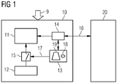
- FIG. 1 shows a programmable logic module, also called FPGA for short below, which is configured via a load bit stream 9.
- the load bit stream 9 structures, also known as modules or components, configured on the programmable logic module, which carry out a wide variety of circuits. These circuits range from simple synchronous counters to highly complex circuits such as microprocessors.
- a clock generator 12, an input interface 14, a controllable switch 15 and a test device 13 are configured on the illustrated module 10.
- a component 11 is configured as a microprocessor.
- the clock generator 12 is connected to the component via the controllable switch 15.
- the input interface 14 has a connection to the external data source 20 and to the component 11. In this case, only one of the two connections is preferably active.
- the input interface 14 is also connected to the test device 13.
- the test device 13 has a connection via the input interface 14 to the data source 20 and a connection to the controllable switch 15.
- the test unit 13 is further configured in such a way that a control signal 17 is output to the controllable switch 15.
- the test device 13 furthermore includes a cryptographic function 19 and a validation parameter 18.
- this processor is not implemented as a circuit directly via structures of the component, but as a so-called soft or soft core CPU that is integrated into the FPGA design.
- a soft CPU is similar to an external CPU and provides a standardized structure.
- This component 11 and subsequently the module itself should now be started via a secure loading process, also called “secure boot”, “trusted boot” or “verified boot”.
- secure boot also called "secure boot”, “trusted boot” or “verified boot”.
- the loading process is initiated by a secure unit, usually referred to as a trust anchor.
- a boot loader and then an operating system and further software are loaded into the FPGA or via the FPGA into further components of an embedded system.
- the external data source 20 can be, for example, a flash memory module or a pure read-only memory, also called ROM, which is implemented on another memory chip or generally an external storage medium such as a USB stick, an SD card, a compact disc or the like be.
- test device 13 After the module 10 has been configured by the load bit stream 9, the test device 13 is automatically activated.
- the connection between clock generator 12 and components 11 is separated by controllable switch 15, so that the component is not active.
- data Via the input interface 14, data are transmitted to the test device 18 in a data bit stream 16.
- the checking device also includes a cryptographic function 19 and a validation parameter 18, which can be, for example, a hash value or a secret key or a public key that is used together with the cryptographic function to check the data stream 16 to be loaded.
- the controllable switch 15, which is connected between the clock generator and the component 11, represents a simple possibility of activating or deactivating the component 11 in a dedicated manner.
- the described invention can also be used with other technical devices for activating or deactivating the component 11. These are not explicitly described, but are known to a person skilled in the field of programmable logic modules.
- FIG. 2 a further embodiment variant 30 of a programmable logic module is shown.
- an additional security unit 31 is implemented in the programmable logic module 30, which forms a dedicated trust anchor.
- This security unit 31 is on the one hand with the component 11, thus for example a soft CPU, and on the other hand connected to the controllable switch 15.
- the controllable switch 15 is in turn connected to the clock generator 12 and is controlled by the test unit 13.
- a test device 13 is generated on the module 10, 30 by a load bit stream 9. This can take place, for example, as part of a synthesis process together with the configuration of the further described modules or components 11, 12, 13, 14, 15, function 18 and validation parameters 19.
- the programmable switch 15 is deactivated so that the component 11, for example a soft CPU, does not go into operation.
- the connection between clock 12 and component 11 is separated.
- the input interface 14 is connected to the test unit 13.
- the input interface 15 can also be connected to the component 11 at the same time. However, data to be read are not processed on component 11, since component 11 is not connected to clock generator 12 and is therefore inactive.
- At least one data bit stream for execution on the at least one component 11 of the module 10, 30 is read into the test device 13 from the external data source 20.
- the boot loader code for a component designed as a soft CPU is loaded from a previously defined memory area of the data source 20.
- the data bit stream 16, here the boot loader code is now processed in the test device 13 with the cryptographic function 19.
- a hash function is implemented as the cryptographic function, for example SHA256 or SHA3, from the data bit stream 16 determine a hash value.
- this hash value is now compared with the validation parameter 19 and the data bit stream is thus checked.
- the validation parameter 19 is here the hash value that was formed using the data bit stream of the boot loader code to be loaded with the same hash function and, for example, was configured with the load bit stream 9 on the module 10, 30.
- the validation parameter 19 is implemented, for example, in the test device 13 or the test unit 13 can access a validation parameter implemented on the module 10, 30 outside the test unit 13.
- the controllable switch 15 is closed, the clock generator 12 is connected to the component 11 and the component 11 is thus started. If the input interface was only connected to the testing device 13, the connection between the input interface 14 and the component 11 is now released so that the data bit stream is now loaded onto the component 11. Loading of the data bit stream 16 is therefore only possible after a successful integrity check of the data bit stream, see step 43. If the check result is negative, the controllable switch 15 remains open and thereby prevents manipulated software from booting from the external data source 20, for example a flash memory.
- the additional security unit 31 is only activated after the data bit stream 16 has been validated. This prevents malicious software from being integrated from the external data source 20 which would abuse or attack the security unit 31, for example a security anchor. The process sequence remains valid as described for module 10.
- a cryptographic hash function such as the HMAC-SHA256, for example, can be used in the test device 13 as a cryptographic function. be used.
- a secret key is provided on the module as a validation parameter.
- the cryptographic function 19 is here, for example, an HMAC-SHA256 algorithm which, with the aid of the secret key and applied to the data bit stream 16, determines what is known as an encrypted message authentication code.
- the same encrypted message authentication code was previously calculated using the same secret key via the data in the data bit stream 16 and stored on the external data source 20.
- the code calculated by the test device 13 is now compared with the previously calculated code.
- the component 11 is activated and the input interface 14 is enabled for the transmission of the data bit stream 16 to the component 11.
- the message authentication code calculated on the external data source 20 can also be loaded with the data bit stream 16 into the checking device 13 and checked there with the validation parameter 18 or the determined code. This has the advantage that any and in particular different data bit streams can be checked by the test device without having to reconfigure the module 10, 30 via the load bit stream.
- the secret key must be applied to the module via the load bit stream. The data bit stream is thus checked using a symmetrical cryptographic process.
- a signature validation function can also be used as the cryptographic function 19.
- the public key of an asymmetric crypto method or key pair is stored as validation parameter 18.
- the data bit stream 16 is transmitted with a signed signature, that is to say includes a digital signature that was determined via the data bit stream 16 with the secret key of the asymmetrical crypto method.
- the signature validation function in the checking device 13 decrypts the digital signature from the data bit stream 16 with the public key and compares this with one in the checking unit 13 via the data bit stream formed hash value. If the values match, the test result is positive and the safety unit 31 or the component 11 is activated.
- Such an asymmetrical method has the advantage over a symmetrical method that no secret key has to be stored and loaded in the load bit stream. Only the public key, which is not a secret and is publicly known, is implemented with the load bit stream 9 on the module 10, 30.
- component 11 In the event of a negative test result, only a partial function of component 11 can be deactivated or one or more components can be activated with incorrect data, so that use of these components is impossible or only possible to a limited extent. Furthermore, not only can data that are to be executed on a component 11 can be checked, but data bit streams that are loaded onto various different components can be checked.
- boot loader or operating system data which are stored on a memory
- data relating to the configuration of other components e.g. an interface chip for WLAN, Ethernet or cellular radio chips.
- the method can also be used to check a hardware configuration and the presence of certain modules or jumpers, so-called jumpers, can be checked.
Landscapes
- Engineering & Computer Science (AREA)
- Software Systems (AREA)
- Computer Security & Cryptography (AREA)
- Theoretical Computer Science (AREA)
- Computer Hardware Design (AREA)
- General Engineering & Computer Science (AREA)
- General Physics & Mathematics (AREA)
- Physics & Mathematics (AREA)
- Radar, Positioning & Navigation (AREA)
- Remote Sensing (AREA)
- Multimedia (AREA)
- Technology Law (AREA)
- Storage Device Security (AREA)
Description
Die Erfindung betrifft einen speicherprogrammbierbaren Baustein mit ladbarem Vertrauensanker sowie ein Verfahren zur geschützten Übertragung von Daten von einer externen Datenquelle auf mindestens eine Komponente eines speicherprogrammierbaren Bausteins.The invention relates to a programmable logic module with a loadable trust anchor and a method for the protected transmission of data from an external data source to at least one component of a programmable logic module.
Eingebettete Systeme werden Computer oder Rechner bezeichnet, die in einem technischen Kontext eingebunden sind und beispielsweise Überwachungs- oder Steuerungsfunktionen in einem Gerät ausführen. Eingebettete Systeme vereinen typischerweise Mikroprozessoren, speicherprogrammierbare Bausteine, auch FPGA bezeichnet, RAM-Speicher, Flash-Speicher und diverse Peripherie in einer Plattform. Der Schutz dieser Systeme spielt eine zunehmend wichtige Rolle, um einen ordnungsgemäßen Betrieb gewährleisten zu können. Eine der wichtigsten Anforderungen dafür ist die Integrität des eingebetteten Systems, d. h. der Schutz gegen nicht-autorisierte Manipulation.Embedded systems are computers or computers that are integrated in a technical context and, for example, perform monitoring or control functions in a device. Embedded systems typically combine microprocessors, programmable logic devices, also known as FPGAs, RAM memories, flash memories and various peripherals in one platform. The protection of these systems plays an increasingly important role in ensuring proper operation. One of the most important requirements for this is the integrity of the embedded system, i. H. protection against unauthorized manipulation.
Um die Integrität eines solchen eingebetteten Systems zu erreichen ist ein sicheres Laden des Systems, das auch als "Secure Boot" oder "Trusted Boot" oder "Verified Boot" bekannt ist. Dabei wird der Ladeprozess von einem nicht änderbaren Vertrauensanker, auch Root-of-Trust genannt, angestoßen. Dieser Vertrauensanker ist beispielsweise ein Stück Hardware, das jeweils die Integrität der als nächstes zu ladenden Stufe der Boot-Software durch die Prüfung eines Hashwertes, beispielsweise eines kryptographischen Hashwertes, einem Message Authentication Code oder einer digitalen Signatur über den Inhalt des zu ladenden Codes und der benötigten Daten, überprüft. Nur bei einer erfolgreichen Überprüfung wird die nächste Stufe gestartet. Diese überprüft wiederum die nächste Stufe, so dass eine Vertrauenskette, eine sogenannte "Chainof-Trust" gewährleistet ist.To achieve the integrity of such an embedded system is a secure loading of the system, which is also known as "Secure Boot" or "Trusted Boot" or "Verified Boot". The loading process is triggered by an unchangeable trust anchor, also known as the root of trust. This trust anchor is, for example, a piece of hardware that ensures the integrity of the next level of the boot software to be loaded by checking a hash value, for example a cryptographic hash value, a message authentication code or a digital signature on the content of the code to be loaded and the required data, checked. The next stage is only started if the check is successful. This in turn checks the next Level, so that a chain of trust, a so-called "chain of trust" is guaranteed.
Ein solcher Secure-Boot-Mechanismus, der die Integrität von Software schützt, die auf einer Soft-CPU in einem FPGA ausgeführt werden soll, ist beispielsweise in einem Artikel mit dem Titel "Introducing the new libero SoC v11.6 Software Toolset", das im Internet unter der URL http://www.microsemi.com/products/fpga-soc/security/secure-boot veröffentlicht ist, beschrieben. Dieser Mechanismus ist direkt nutzbar und führt zu einem guten Schutzniveau.One such secure boot mechanism, which protects the integrity of software to be executed on a soft CPU in an FPGA, is, for example, in an article entitled "Introducing the new libero SoC v11.6 Software Toolset", the on the Internet under the URL http://www.microsemi.com/products/fpga-soc/security/secure-boot is described. This mechanism can be used directly and leads to a good level of protection.
Essentieller Punkt dieser Lösung ist, dass der initiale Boot-Code und eventuell benötigte kryptographische Schlüssel manipulationsgeschützt implementiert sein müssen. Dies ist bisher nur möglich, wenn der ausführende Mikroprozessor bzw. ein speicherprogrammierbarer Baustein, auf dem der ausführende Mikroprozessor ausgebildet ist, vom Hersteller bereits mit einem in Hardware integrierten Vertrauensanker ausgestattet wurde, z. B. einem nur lesbaren Speicher für Ladecode, auch Boot ROM bezeichnet. Dies ist jedoch oft nicht der Fall oder erfordert den Kauf einer teuren Variante.The essential point of this solution is that the initial boot code and any required cryptographic key must be implemented in a tamper-proof manner. So far, this has only been possible if the executing microprocessor or a programmable logic module on which the executing microprocessor is designed has already been equipped by the manufacturer with a trust anchor integrated into the hardware, e.g. B. a read-only memory for loading code, also called Boot ROM. However, this is often not the case or requires purchasing an expensive variant.
Aus der
Die
Die Aufgabe der vorliegenden Erfindung ist es daher, einen einfachen und günstigen Vertrauensanker in einem eingebetteten System, insbesondere im Zusammenspiel mit einer Soft-CPU, in einem speicherprogrammierbaren Baustein zu schaffen.The object of the present invention is therefore to create a simple and inexpensive trust anchor in an embedded system, in particular in interaction with a soft CPU, in a programmable logic module.
Die Aufgabe wird durch die in den unabhängigen Ansprüchen beschriebenen Maßnahmen gelöst. In den Unteransprüchen sind vorteilhafte Weiterbildungen der Erfindung dargestellt.The object is achieved by the measures described in the independent claims. Advantageous developments of the invention are presented in the subclaims.
Der erfindungsgemäße speicherprogrammierbare Baustein umfasst eine Prüfeinrichtung und mindestens eine weitere Komponente, wobei die Prüfeinrichtung durch einen Ladebitstrom auf dem Baustein erzeugbar ist und die Prüfeinrichtung derart ausgebildet ist, mindestens einen Datenbitstrom zum Ausführen auf der mindestens einen Komponente des Bausteins von einer externen Datenquelle einzulesen, den Datenbitstrom zu prüfen und bei positivem Prüfergebnis ein Steuersignal auszugeben, das die Komponente mit den Daten des Datenbitstroms aktiviert.The programmable logic module according to the invention comprises a test device and at least one further component, the test device being able to be generated by a load bit stream on the module and the test device being designed in such a way that at least one data bit stream for executing on the at least one component of the module from an external Read in the data source, check the data bit stream and, if the test result is positive, output a control signal that activates the component with the data of the data bit stream.
Die Prüfeinrichtung stellt somit einen Vertrauensanker dar, der mit dem Ladebitstrom auf einen speicherprogrammierbaren Baustein geladen wird. Die mindestens eine Komponente ist beispielsweise eine Soft-CPU, d.h. ein Mikroprozessor, der in das FPGA-Design eingebunden ist. Die Komponente ist dabei nach dem Laden der Prüfeinrichtung deaktiviert und wird erst nach einer positiven Prüfung des Datenbitstroms durch die Prüfeinheit aktiviert. Dadurch wird ein Integritätsschutz für Software, beispielsweise für einen Boot Loader oder ein Betriebssystem, die auf einer externen Datenquelle gespeichert sind, erreicht. Dieser Integritätsschutz kann nur durch ein sehr aufwendiges Reverse Engineering des FPGA Ladebitstroms gebrochen werden. Somit wird die Sicherheit für ein Secure Boot auf kostengünstigen speicherprogrammierbaren Bausteinen ohne dedizierte Secure Boot Unterstützung deutlich erhöht. Ein weiterer Vorteil besteht darin, dass das gesamte eingebettete System nur minimal angepasst werden muss, keine zusätzlichen Hardwarebauteile nötig sind und die Prüfeinrichtung als Modul auf dem FPGA sehr ressourcensparend implementiert werden kann.The test device thus represents a trust anchor that is loaded onto a programmable logic module with the load bit stream. The at least one component is, for example, a soft CPU, i.e. a microprocessor integrated into the FPGA design. The component is deactivated after loading the test device and is only activated after a positive test of the data bit stream by the test unit. In this way, integrity protection for software, for example for a boot loader or an operating system, which is stored on an external data source, is achieved. This integrity protection can only be broken by a very complex reverse engineering of the FPGA load bit stream. This significantly increases the security for a secure boot on inexpensive programmable logic modules without dedicated secure boot support. Another advantage is that the entire embedded system only has to be adjusted minimally, no additional hardware components are required and the test device can be implemented as a module on the FPGA in a very resource-saving manner.
In einer vorteilhaften Weiterbildung umfasst die Prüfeinrichtung eine kryptographische Funktion und ist derart ausgebildet, die Daten des Datenstroms mit Hilfe eines Validierungsparameters und der kryptographischen Funktion zu prüfen.In an advantageous development, the test device includes a cryptographic function and is designed to test the data of the data stream with the aid of a validation parameter and the cryptographic function.
Somit kann der für die Komponente vorgesehene Datenbitstrom vor einem Aktivieren auf der Komponente flexibel in der Prüfeinrichtung auf Übereinstimmung mit dem erwarteten Datenbitstrom getestet werden.Thus, the data bit stream provided for the component can be flexibly tested in the test device for agreement with the expected data bit stream before it is activated on the component.
In einer vorteilhaften Ausführungsform ist die kryptographische Funktion eine Hashfunktion und der Validierungsparameter ein mit der Hashfunktion erstellter Hashwert des Datenbitstroms.In an advantageous embodiment, the cryptographic function is a hash function and the validation parameter a hash value of the data bit stream created with the hash function.
Eine Hashfunktion ist dabei eine wenig komplexe Funktion, die einfach und Ressourcen-sparend implementiert werden kann.A hash function is a less complex function that can be implemented easily and in a resource-saving manner.
In einer alternativen Ausführungsform ist die kryptographische Funktion eine kryptographische Hashfunktion und der Validierungsparameter ein geheimer Schlüssel.In an alternative embodiment, the cryptographic function is a cryptographic hash function and the validation parameter is a secret key.
Dabei wird beispielsweise ein kryptographischer Nachrichten-Authentisierungscode HMAC oder ein anderer kryptographischer Parameter durch die kryptographische Hashfunktion unter Verwendung des geheimen Schlüssels über den Datenbitstrom erzeugt und gegen einen in der Datenquelle gespeicherten und/oder im Datenbitstrom enthaltene originalen HMAC verglichen. Dies hat den Vorteil, dass kein spezifischer Hashwert auf dem speicherprogrammierbaren Baustein oder direkt auf der Prüfeinrichtung implementiert ist und insbesondere dieser spezifische Hashwert nicht in einem Ladebitstrom auf den Baustein übertragen werden muss. Es können somit unterschiedliche Datenbitströme mit nur einem Validierungsparameter geprüft werden.For example, a cryptographic message authentication code HMAC or another cryptographic parameter is generated by the cryptographic hash function using the secret key over the data bit stream and compared with an original HMAC stored in the data source and / or contained in the data bit stream. This has the advantage that no specific hash value is implemented on the programmable logic module or directly on the test device and, in particular, this specific hash value does not have to be transmitted to the module in a load bit stream. Different data bit streams can thus be checked with just one validation parameter.
In einer vorteilhaften Ausführungsform ist die kryptographische Funktion eine Signatur-Validierungsfunktion und der Validierungsparameter ein öffentlicher Schlüssel.In an advantageous embodiment, the cryptographic function is a signature validation function and the validation parameter is a public key.
Dies hat den Vorteil, dass kein geheimer Schlüssel im Ladebitstrom auf den Baustein bzw. die Prüfeinrichtung übertragen werden muss und daher auch nicht ausgelesen und manipuliert werden kann.This has the advantage that no secret key has to be transmitted in the load bit stream to the module or the test device and therefore cannot be read out or manipulated.
In einer vorteilhaften Ausführungsform ist der Validierungsparameter mit dem Ladebitstrom auf dem Baustein implementierbar.In an advantageous embodiment, the validation parameter can be implemented on the module with the load bit stream.
Dies ermöglicht es, flexibel bei der Synthese des speicherprogrammierbaren Bausteins den Validierungsparameter einzubringen. D.h., bereits bei der Konfiguration des Bausteins wird über den Ladebitstrom der Validierungsparameter für die nachfolgend auf der Komponente zu ladende Software erstellt. Durch eine automatische Deaktivierung der Komponente nach der initialen Konfiguration und einer expliziten Aktivierung der Komponente nach erfolgreicher Prüfung ist somit ein ungeprüftes Laden bzw. Booten der Komponente kaum möglich.This enables the validation parameters to be introduced flexibly in the synthesis of the programmable logic module. This means that the validation parameters for the software to be subsequently loaded onto the component are created using the load bit stream when the block is configured. With an automatic deactivation of the component after the initial configuration and an explicit activation of the component after a successful test, an unchecked loading or booting of the component is hardly possible.
In einer vorteilhaften Ausführungsform umfasst der speicherprogrammierbare Baustein eine zusätzliche Sicherheitseinheit, die mit der zu programmierenden Komponente und der Prüfeinrichtung verbunden ist und durch das Steuersignal der Prüfeinrichtung aktivierbar ist.In an advantageous embodiment, the programmable logic module comprises an additional safety unit which is connected to the component to be programmed and the test device and can be activated by the control signal of the test device.
Somit können manipulierte Daten wie bspw. bösartige Software erkannt werden und eine Manipulation des Vertrauensankers verhindert werden.This means that manipulated data such as malicious software can be recognized and manipulation of the trust anchor prevented.
In einer vorteilhaften Ausführungsform ist die Prüfeinrichtung derart ausgebildet, bei einem negativen Prüfergebnis ein Steuersignal zum Deaktivieren der Komponente oder zum Deaktivieren mindestens einer Teilfunktion der Komponente zu erzeugen oder die Komponente mit einem zweiten Datenbitstrom zu aktivieren, der eine Benutzung der Komponente unmöglich oder nur eingeschränkt möglich macht.In an advantageous embodiment, the test device is designed to generate a control signal for deactivating the component or for deactivating at least one partial function of the component in the event of a negative test result or to activate the component with a second data bit stream that makes it impossible or only possible to use the component to a limited extent power.
Somit ist ein aktives Deaktivieren einer bereits aktiven Komponente möglich.Active deactivation of an already active component is thus possible.
In einer weiteren vorteilhaften Ausführungsform umfasst der speicherprogrammierbare Baustein einen steuerbaren Schalter, der durch das Steuersignal der Prüfeinrichtung die Komponente oder den Vertrauensanker mit einem Taktgeber verbindet und so die Komponente oder den Vertrauensanker aktiviert oder trennt und somit deaktiviert.In a further advantageous embodiment, the programmable logic module comprises a controllable switch which connects the component or the trust anchor to a clock generator through the control signal of the test device and thus activates or disconnects and thus deactivates the component or the trust anchor.
Ein steuerbarer Schalter ist einfach konfigurierbar und stellt eine einfache Möglichkeit zur Aktivierung bzw. Deaktivierung der Komponente dar.A controllable switch is easy to configure and provides a simple way to activate or deactivate the component.
Das erfindungsgemäße Verfahren zur geschützten Übertragung von Daten von einer externen Datenquelle auf mindestens eine Komponente eines speicherprogrammierbaren Bausteins umfasst die Schritte, Erzeugen einer Prüfeinrichtung auf dem Baustein durch einen Ladebitstrom, Einlesen mindestens eines Datenbitstroms zum Ausführen auf der mindestens einen Komponente des Bausteins von einer externen Datenquelle in die Prüfeinrichtung, Prüfen des Datenbitstroms in der Prüfeinrichtung und Ausgabe eines Steuersignals bei positivem Prüfergebnis zum Aktivieren der Komponente mit den Daten des Datenbitstroms.The inventive method for the protected transmission of data from an external data source to at least one component of a programmable logic module comprises the steps of generating a test device on the module using a load bit stream, reading in at least one data bit stream for execution on the at least one component of the module from an external data source into the testing device, testing the data bit stream in the testing device and outputting a control signal if the test result is positive to activate the component with the data of the data bit stream.
Ist die Komponente beispielsweise eine Soft-CPU auf einem FPGA, so kann durch das Verfahren der Vertrauensanker in den Ladebitstrom des FPGAs verlagert werden. Dadurch ist ein Integritätsschutz für die in der Datenquelle enthaltene Software, wie Boot Loader oder auch Konfiguration eines FPGA Moduls möglich, der nur durch aufwendige Maßnahmen gebrochen werden kann.If the component is, for example, a soft CPU on an FPGA, the method can shift the trust anchor into the load bit stream of the FPGA. This enables integrity protection for the software contained in the data source, such as the boot loader or configuration of an FPGA module, which can only be broken through complex measures.
In einer vorteilhaften Ausführungsform werden die Daten des Datenbitstroms mit Hilfe einer kryptographischen Funktion und einem Validierungsparameter in der Prüfungseinheit geprüft.In an advantageous embodiment, the data of the data bit stream are checked in the checking unit with the aid of a cryptographic function and a validation parameter.
Es stehen somit verschiedene auch bekannte Verfahren zur Auswahl, die entsprechend dem Schutzbedarf der zu ladenden Daten oder auch abhängig von der Leistungsfähigkeit des programmierbaren Bausteins ausgewählt werden können.There are thus various well-known methods to choose from, which can be selected according to the protection requirements of the data to be loaded or also depending on the performance of the programmable module.
In einer vorteilhaften Ausführungsform wird der Validierungsparameter über den Ladebitstrom auf dem Baustein implementiert.In an advantageous embodiment, the validation parameter is implemented on the module via the load bit stream.
Dies ermöglicht es, individuell bei jedem Aktivieren des speicherprogrammierbaren Bausteins, unterschiedliche Daten, z.B. unterschiedliche Ausprägungen eines Bootloaders oder Betriebssystems, auf eine Komponente zu laden und diese Daten vorher individuell zu prüfen.This makes it possible, each time the programmable logic module is activated, different data, For example, to load different versions of a boot loader or operating system onto a component and to check this data individually beforehand.
In einer vorteilhaften Ausführungsform wird in der Prüfeinrichtung aus den Daten des Datenbitstroms mittels einer Hashfunktion als kryptographischer Funktion ein Prüfwert erzeugt und gegenüber dem Validierungsparameter geprüft.In an advantageous embodiment, a test value is generated in the test device from the data of the data bit stream using a hash function as a cryptographic function and is checked against the validation parameter.
In einer weiteren vorteilhaften Ausführungsform wird als kryptographische Funktion eine kryptographische Hashfunktion und als Validierungsparameter ein geheimer Schlüssel verwendet und im Datenbitstrom ein mit demselben geheimen Schlüssel erzeugter Vergleichswert an die Prüfeinrichtung übertragen.In a further advantageous embodiment, a cryptographic hash function is used as the cryptographic function and a secret key is used as the validation parameter, and a comparison value generated with the same secret key is transmitted to the test device in the data bit stream.
Dies hat den Vorteil, dass unterschiedliche Daten eines Datenbitstroms übertragen und geprüft werden können, ohne den Validierungsparameter, hier insbesondere den geheimen Schlüssel, anpassen zu müssen. Es ist somit kein neuer Ladestrom zur Konfiguration eines geänderten Validierungsparameters notwendig.This has the advantage that different data of a data bit stream can be transmitted and checked without having to adapt the validation parameters, here in particular the secret key. There is therefore no need for a new charging current to configure a changed validation parameter.
In einer vorteilhaften Ausführungsform ist die kryptographische Funktion eine Schlüsselvalidierungsfunktion und der Validierungsparameter ein öffentlicher Schlüssel. Der Datenbitstrom wird signiert mit einem dem öffentlichen Schlüssel entsprechenden geheimen Schlüssel an die Prüfeinheit übertragen.In an advantageous embodiment, the cryptographic function is a key validation function and the validation parameter is a public key. The data bit stream is signed and transmitted to the test unit with a secret key corresponding to the public key.
Eine Schlüsselvalidierungsfunktion für ein asymmetrisches Verschlüsselungsverfahren, beispielsweise einer Private-Key-Infrastruktur, bietet einen besonders hohen Integritätsschutz und hat wie das zuvor beschriebene symmetrische Verfahren mit geheimem Schlüssel den Vorteil, den Validierungsparameter bei geändertem Datenbitstrom nicht nochmals in den Baustein einbringen zu müssen. Des Weiteren muss bei dem genannten asymmetrischen Verfahren lediglich der öffentliche Schlüssel jedoch kein geheimer Schlüssel über den Ladebitstrom in den Baustein eingebracht werden.A key validation function for an asymmetric encryption method, for example a private key infrastructure, offers a particularly high level of integrity protection and, like the previously described symmetric method with a secret key, has the advantage of not having to re-enter the validation parameters in the module when the data bit stream changes. Furthermore, in the case of the aforementioned asymmetrical method, only the public key, but no secret key, has to be introduced into the module via the load bit stream.
In einer vorteilhaften Ausführungsform enthält der Datenbitstrom Daten eines Startprogramms, auch Boot Loader genannt, eines Betriebssystems oder einer Bausteinkonfiguration und die externe Datenquelle ist insbesondere eine Speichereinheit außerhalb des speicherprogrammierbaren Bausteins oder ein externes Speichermedium.In an advantageous embodiment, the data bit stream contains data from a start program, also called a boot loader, an operating system or a module configuration, and the external data source is in particular a memory unit outside the programmable logic module or an external storage medium.
Des Weiteren wird ein Computerprogrammprodukt beansprucht, das Programmcodeteile umfasst, die geeignet sind, die Schritte des beanspruchten Verfahrens durchzuführen.Furthermore, a computer program product is claimed which comprises program code parts which are suitable for carrying out the steps of the claimed method.
Ausführungsbeispiele des erfindungsgemäßen speicherprogrammierbaren Bausteins sowie des beanspruchten Verfahrens sind in den Zeichnungen beispielhaft dargestellt und werden anhand der nachfolgenden Beschreibung näher erläutert. Es zeigen:
- Figur 1
- ein erstes Ausführungsbeispiel eines erfindungsgemäßen speicherprogrammierbaren Bausteins in Blockdarstellung,
- Figur 2
- ein zweites Ausführungsbeispiel eines erfindungsgemäßen speicherprogrammierbaren Bausteins mit zusätzlicher Sicherheitseinheit in Blockdarstellung, und
- Figur 3
- ein Ausführungsbeispiel des erfindungsgemäßen Verfahrens als Ablaufdiagramm.
- Figure 1
- a first embodiment of a programmable logic module according to the invention in a block diagram,
- Figure 2
- a second embodiment of a programmable logic module according to the invention with an additional safety unit in a block diagram, and
- Figure 3
- an embodiment of the method according to the invention as a flow chart.
Alle beschriebenen und/oder gezeichneten Merkmale können im Rahmen der Erfindung vorteilhaft miteinander kombiniert werden. Die Erfindung ist nicht auf die beschriebenen Ausführungsbeispiele beschränkt.All of the features described and / or drawn can advantageously be combined with one another within the scope of the invention. The invention is not restricted to the exemplary embodiments described.
Die Prüfeinrichtung 13 weist eine Verbindung über die Eingabe-Schnittstelle 14 zur Datenquelle 20 und eine Verbindung zum steuerbaren Schalter 15 auf. Die Prüfeinheit 13 ist des Weiteren derart konfiguriert, ein Steuersignal 17 an den steuerbaren Schalter 15 auszugeben. Die Prüfeinrichtung 13 umfasst des Weiteren eine kryptographische Funktion 19 sowie einen Validierungsparameter 18.The
Im dargestellten Beispiel sei dieser Prozessor nicht als Schaltung direkt über Strukturen des Bausteins realisiert, sondern als sogenannte Soft- oder Softcore-CPU, die in das FPGA-Design eingebunden ist. Eine Soft-CPU gleicht einer externen CPU und stellt eine standardisierte Struktur bereit. Diese Komponente 11 und nachfolgend der Baustein selbst soll nun über einen sicheren Ladevorgang, auch "Secure Boot", "Trusted Boot" oder "Verified Boot" genannt, gestartet werden. Um die Integrität eines Systems zu gewährleisten, wird der Ladeprozess von einer sicheren Einheit, üblicherweise als Vertrauensanker bezeichnet, angestoßen. Dazu wird im ersten Schritt ein Boot Loader und nachfolgend ein Betriebssystem und weitere Software in den FPGA bzw. über den FPGA in weitere Bausteine eines eingebetteten Systems geladen. Daten, etwa der Boot Loader, das Betriebssystem oder auch weitere Daten sind dabei auf einer externen Datenquelle 20 gespeichert und von dort über einen Datenbitstrom 16 in den Baustein 10 geladen. Die externe Datenquelle 20 kann beispielsweise als ein Flash-Speicherbaustein oder ein reiner Lesespeicher, auch ROM genannt, der auf einem anderen Speicherchip implementiert ist oder allgemein ein externes Speichermedium, wie beispielsweise ein USB-Stick, eine SD-Karte, eine Compact Disc oder Ähnliches sein.In the example shown, this processor is not implemented as a circuit directly via structures of the component, but as a so-called soft or soft core CPU that is integrated into the FPGA design. A soft CPU is similar to an external CPU and provides a standardized structure. This
Nach der Konfiguration des Bausteins 10 durch den Ladebitstrom 9 wird die Prüfeinrichtung 13 automatisch aktiviert. Die Verbindung zwischen Taktgeber 12 und Komponenten 11 ist durch den steuerbaren Schalter 15 getrennt, sodass die Komponente nicht aktiv ist. Über die Eingabeschnittstelle 14 werden Daten in einem Datenbitstrom 16 an die Prüfeinrichtung 18 übermittelt. Die Prüfeinrichtung umfasst des Weiteren eine kryptographische Funktion 19 sowie einen Validierungsparameter 18, der beispielsweise ein Hashwert oder ein geheimer Schlüssel oder ein öffentlicher Schlüssel sein kann, der zusammen mit der kryptographischen Funktion zur Prüfung des zu ladenden Datenstroms 16 verwendet wird.After the
Der steuerbare Schalter 15, der zwischen den Taktgeber und die Komponente 11 zwischengeschaltet ist, stellt eine einfache Möglichkeit dar, die Komponente 11 dediziert zu aktivieren bzw. zu deaktivieren. Die beschriebene Erfindung kann auch mit anderen technischen Einrichtungen zur Aktivierung bzw. Deaktivierung der Komponente 11 verwendet werden. Diese sind nicht explizit beschrieben, aber einem Fachmann auf dem Gebiet von speicherprogrammierbaren Bausteinen bekannt.The
In
Anhand von
Bei einem ersten Verfahrensschritt 40 wird durch einen Ladebitstrom 9 eine Prüfeinrichtung 13 auf dem Baustein 10, 30 erzeugt. Dies kann beispielsweise im Rahmen eines Syntheseprozesses zusammen mit der Konfiguration der weiteren beschriebenen Module bzw. Komponenten 11, 12, 13, 14, 15, Funktion 18 und Validierungsparameter 19 erfolgen. Der programmierbare Schalter 15 ist deaktiviert, so dass die Komponente 11, beispielsweise eine Soft-CPU, nicht in Betrieb geht. In den in
Nachfolgend wird im Verfahrensschritt 41 mindestens ein Datenbitstrom zum Ausführen auf der zumindest einen Komponente 11 des Bausteins 10, 30 von der externen Datenquelle 20 in die Prüfeinrichtung 13 eingelesen. Es wird also beispielsweise der Boot Loader Code für eine als Soft-CPU ausgebildete Komponente aus einem zuvor definierten Speicherbereich der Datenquelle 20 geladen. In der Prüfeinrichtung 13 wird nun der Datenbitstrom 16, hier der Boot Loader Code, mit der kryptographischen Funktion 19 verarbeitet. Beispielsweise ist als kryptographische Funktion eine Hashfunktion implementiert, beispielsweise SHA256 oder SHA3, die aus dem Datenbitstrom 16 einen Hashwert ermitteln. Im Verfahrensschritt 42 wird nun dieser Hashwert mit dem Validierungsparameter 19 verglichen und somit der Datenbitstrom geprüft. Der Validierungsparameter 19 ist hier der Hashwert, der über den Datenbitstrom des zu ladenden Boot Loader Codes mit der gleichen Hashfunktion gebildet wurde und beispielsweise mit dem Ladebitstrom 9 auf dem Baustein 10, 30 konfiguriert wurde. Der Validierungsparameter 19 ist beispielsweise in der Prüfeinrichtung 13 implementiert oder die Prüfeinheit 13 kann auf einen außerhalb der Prüfeinheit 13 auf dem Baustein 10, 30 implementierten Validierungsparameter zugreifen.Subsequently, in
Bei einem positiven Prüfergebnis wird der steuerbare Schalter 15 geschlossen, der Taktgeber 12 mit der Komponente 11 verbunden und somit die Komponente 11 gestartet. War die Eingabeschnittstelle lediglich mit der Prüfeinrichtung 13 verbunden, so nun wird die Verbindung zwischen der Eingabeschnittstelle 14 und der Komponente 11 freigegeben, so dass der Datenbitstrom nun auf die Komponente 11 geladen wird. Ein Laden des Datenbitstroms 16 ist somit erst nach einer erfolgreichen Integritätsprüfung des Datenbitstroms möglich, siehe Schritt 43. Bei einem negativen Prüfungsergebnis bleibt der steuerbare Schalter 15 offen und verhindert dadurch das Booten manipulierter Software aus der externen Datenquelle 20, beispielsweise einen Flash-Speicher.If the test result is positive, the
Wird das Verfahren auf den in
Zur Überprüfung des Datenbitstroms 16 kann in der Prüfeinrichtung 13 beispielsweise als kryptographische Funktion eine kryptographische Hashfunktion, wie beispielsweise die HMAC-SHA256, verwendet werden. Als Validierungsparameter ist in diesem Fall ein geheimer Schlüssel auf dem Baustein bereitgestellt. Die kryptographische Funktion 19 ist hier beispielsweise ein HMAC-SHA256 Algorithmus, der mit Hilfe des geheimen Schlüssels und angewandt auf den Datenbitstrom 16 einen sogenannten verschlüsselten Message Authentication Code ermittelt. Der gleiche verschlüsselte Message Authentication Code wurde vorher mit demselben geheimen Schlüssel über die Daten den Datenbitstrom 16 berechnet und auf der externen Datenquelle 20 gespeichert. Der von der Prüfeinrichtung 13 berechnete Code wird nun mit dem vorher berechneten Code verglichen. Bei einem Übereinstimmen und somit einem positiven Prüfergebnis wird die Komponente 11 aktiviert und die Eingabeschnittstelle 14 zur Übertragung des Datenbitstroms 16 auf die Komponente 11 freigegeben. Der auf der externen Datenquelle 20 berechnete Nachrichten-Authentisierungscode kann auch mit dem Datenbitstrom 16 in die Prüfeinrichtung 13 geladen werden und dort mit dem Validierungsparameter 18 bzw. dem ermittelten Code geprüft werden. Dies hat den Vorteil, dass beliebige und insbesondere unterschiedliche Datenbitströme durch die Prüfeinrichtung geprüft werden können ohne den Baustein 10, 30 über den Ladebitstrom neu konfigurieren zu müssen. Andererseits muss der geheime Schlüssel über den Ladebitstrom auf den Baustein aufgebracht werden. Der Datenbitstrom wird somit durch ein symmetrisches kryptographisches Verfahren überprüft.To check the data bit
Als kryptographische Funktion 19 kann auch eine Signaturvalidierungsfunktion verwendet werden. Dabei ist als Validierungsparameter 18 der öffentliche Schlüssel eines asymmetrischen Kryptoverfahrens bzw. Schlüsselpaars gespeichert. Der Datenbitstrom 16 wird dabei signiert übertragen, umfasst also eine digitale Signatur, die mit dem geheimen Schlüssel des asymmetrischen Kryptoverfahrens über den Datenbitstrom 16 ermittelt wurde. Die Signaturvalidierungsfunktion in der Prüfeinrichtung 13 entschlüsselt mit dem öffentlichen Schlüssel die digitale Signatur aus dem Datenbitstrom 16 und vergleicht diese mit einem in der Prüfeinheit 13 über den Datenbitstrom gebildeten Hashwert. Stimmen die Werte überein, liegt ein positives Prüfergebnis vor und die Sicherheitseinheit 31 bzw. die Komponente 11 wird aktiviert. Ein solches asymmetrisches Verfahren hat gegenüber einem symmetrischen Verfahren den Vorteil, dass im Ladebitstrom kein geheimer Schlüssel gespeichert und geladen werden muss. Lediglich der öffentliche Schlüssel, der kein Geheimnis darstellt und öffentlich bekannt ist, wird mit dem Ladebitstrom 9 auf den Baustein 10, 30 implementiert.A signature validation function can also be used as the cryptographic function 19. The public key of an asymmetric crypto method or key pair is stored as
Bei einem negativen Prüfergebnis kann auch lediglich eine Teilfunktion der Komponente 11 deaktiviert werden oder eine oder mehrere Komponenten mit falschen Daten aktiviert werden, so dass eine Benutzung dieser Komponenten unmöglich oder nur eingeschränkt möglich wird. Des Weiteren können nicht nur Daten, die auf einer Komponente 11 zur Ausführung gebracht werden sollen, überprüft werden, sondern Datenbitströme, die auf verschiedene unterschiedliche Komponenten geladen werden, geprüft werden.In the event of a negative test result, only a partial function of
Statt den Bootloader- oder Betriebssystem-Daten, die auf einem Speicher abgelegt sind, können auch Daten der Konfiguration anderer Bausteine z.B. eines Interface Chips für WLAN, Ethernet- oder auch Mobilfunkchips überprüft werden. Ebenfalls kann das Verfahren zur Prüfung einer Hardware-Konfiguration verwendet werden und das Vorhandensein von bestimmten Bausteinen oder Sprungmarkern, so genannten Jumpern, überprüft werden.Instead of the boot loader or operating system data, which are stored on a memory, data relating to the configuration of other components, e.g. an interface chip for WLAN, Ethernet or cellular radio chips. The method can also be used to check a hardware configuration and the presence of certain modules or jumpers, so-called jumpers, can be checked.
Alle beschriebenen und/oder gezeichneten Merkmale können im Rahmen der Erfindung vorteilhaft miteinander kombiniert werden. Die Erfindung ist nicht auf die beschriebenen Ausführungsbeispiele beschränkt.All of the features described and / or drawn can advantageously be combined with one another within the scope of the invention. The invention is not restricted to the exemplary embodiments described.
Claims (17)
- Stored-program module with a loadable trust anchor, comprising a checking device (13) and at least one further component (11), wherein
the checking device (13) can be generated on the module (10) by means of a loading bit stream (9) and the at least one component (11) is automatically deactivated after loading, the checking device (13) is designed to read in at least one data bit stream (16) for execution on the at least one component (11) of the module (10) from an external data source (20), to check the data bit stream (16) and, in the event of a positive checking result, to output a control signal (17) which activates the component (11). - Stored-program module according to Claim 1, wherein the checking device (13) comprises a cryptographic function (19) and is designed to check the data in the data stream with the aid of a validation parameter (18) and the cryptographic function (19).
- Stored-program module according to Claim 2, wherein the cryptographic function (19) is a hash function and the validation parameter (18) is a hash value of the data bit stream (16) created using the hash function.
- Stored-program module according to Claim 2, wherein the cryptographic function (19) is a cryptographic hash function and the validation parameter (18) is a secret key.
- Stored-program module according to Claim 2, wherein the cryptographic function (19) is a signature validation function and the validation parameter (18) is a public key.
- Stored-program module according to Claim 2, wherein a validation parameter can be implemented on the module (10) using the loading bit stream (9).
- Stored-program module according to one of Claims 1 to 6, comprising an additional security unit (31) which is connected to the component to be programmed and to the checking device (13) and can be activated by the control signal (17) from the checking device (13).
- Stored-program module according to one of Claims 1 to 7, wherein the checking device (13) is designed, in the event of a negative checking result, to generate a control signal (17) for deactivating the component (11, 31) or at least one sub-function of the component (11, 31) or to activate the component (11, 31) with a second data bit stream which makes it impossible to use the component (11, 31) or makes it possible to use the component (11, 31) only to a limited extent.
- Stored-program module according to one of Claims 1 to 8, comprising a controllable switch (15) which connects the component (11) or the trust anchor to a clock generator (12) by virtue of the control signal (17) from the checking device (13) and therefore activates or disconnects and therefore deactivates the component or the trust anchor.
- Method for transmitting data from an external data source to at least one component (11) of a stored-program module in a protected manner, having the steps of:- generating (41) a checking device (13) on the module (10) by means of a loading bit stream (9) and deactivating the at least one component (11),- reading in (42) at least one data bit stream (16) for execution on the at least one component (11) of the module (10) from an external data source (20) into the checking device (13),- checking (43) the data bit stream (16) in the checking device; and- outputting (44) a control signal (17), in the event of a positive checking result, for the purpose of activating the component (11) with the data in the data bit stream (16) .
- Method according to Claim 10, wherein the data in the data stream are checked in the checking unit (13) with the aid of a cryptographic function and a validation parameter.
- Method according to Claim 11, wherein the validation value (18) is implemented on the module using the loading bit stream (9).
- Method according to one of Claims 10 to 12, wherein a check value is generated from the data in the data bit stream (16) in the checking device (13) by means of a hash function as a cryptographic function (19) and is checked with respect to the validation parameter (18).
- Method according to one of Claims 10 to 12, wherein the cryptographic function (19) is a cryptographic hash function and the validation parameter (18) is a secret key, and a comparison value generated using the same secret key is transmitted in the data bit stream (16) to the checking device (13) .
- Method according to one of Claims 10 to 12, wherein the cryptographic function (19) is a key validation function and the validation parameter (18) is a public key, and the data bit stream is transmitted to the checking device (13) in a manner signed with a secret key corresponding to the public key.
- Method according to either of Claims 10 and 15, wherein the data bit stream (16) contains data from a starting program, an operating system or a module configuration, and the external data source is a storage unit (20) outside the module or an external storage medium.
- Computer program product comprising program code parts which are suitable for carrying out the steps of the method according to one of Claims 10 to 16.
Applications Claiming Priority (2)
| Application Number | Priority Date | Filing Date | Title |
|---|---|---|---|
| DE102015224300.1A DE102015224300A1 (en) | 2015-12-04 | 2015-12-04 | Programmable logic device and method for protected transmission of data to a programmable logic device |
| PCT/EP2016/074391 WO2017092917A1 (en) | 2015-12-04 | 2016-10-12 | Stored-program module and method for the secured transfer of data to a stored-program module |
Publications (2)
| Publication Number | Publication Date |
|---|---|
| EP3347848A1 EP3347848A1 (en) | 2018-07-18 |
| EP3347848B1 true EP3347848B1 (en) | 2020-08-26 |
Family
ID=57138050
Family Applications (1)
| Application Number | Title | Priority Date | Filing Date |
|---|---|---|---|
| EP16782036.4A Active EP3347848B1 (en) | 2015-12-04 | 2016-10-12 | Stored-program module and method for the secured transfer of data to a stored-program module |
Country Status (4)
| Country | Link |
|---|---|
| EP (1) | EP3347848B1 (en) |
| DE (1) | DE102015224300A1 (en) |
| ES (1) | ES2830433T3 (en) |
| WO (1) | WO2017092917A1 (en) |
Family Cites Families (6)
| Publication number | Priority date | Publication date | Assignee | Title |
|---|---|---|---|---|
| DE69329778T2 (en) * | 1992-09-29 | 2001-04-26 | Seiko Epson Corp., Tokio/Tokyo | SYSTEM AND METHOD FOR HANDLING LOADS AND / OR STORES IN A SUPER-SCALAR MICROPROCESSOR |
| US7773754B2 (en) * | 2002-07-08 | 2010-08-10 | Broadcom Corporation | Key management system and method |
| EP1679573B1 (en) * | 2005-01-07 | 2007-06-27 | Telefonaktiebolaget LM Ericsson (publ) | Updating memory contents of a processing device |
| US8646094B2 (en) * | 2011-12-07 | 2014-02-04 | Owl Computing Technologies, Inc. | Method and apparatus for preventing unauthorized access to information stored in a non-volatile memory |
| DE102013213314A1 (en) * | 2013-07-08 | 2015-01-08 | Siemens Aktiengesellschaft | Deposit at least one computable integrity measure in a memory area of a memory |
| US9830456B2 (en) * | 2013-10-21 | 2017-11-28 | Cisco Technology, Inc. | Trust transference from a trusted processor to an untrusted processor |
-
2015
- 2015-12-04 DE DE102015224300.1A patent/DE102015224300A1/en not_active Withdrawn
-
2016
- 2016-10-12 EP EP16782036.4A patent/EP3347848B1/en active Active
- 2016-10-12 WO PCT/EP2016/074391 patent/WO2017092917A1/en unknown
- 2016-10-12 ES ES16782036T patent/ES2830433T3/en active Active
Non-Patent Citations (1)
| Title |
|---|
| None * |
Also Published As
| Publication number | Publication date |
|---|---|
| DE102015224300A1 (en) | 2017-06-08 |
| EP3347848A1 (en) | 2018-07-18 |
| ES2830433T3 (en) | 2021-06-03 |
| WO2017092917A1 (en) | 2017-06-08 |
Similar Documents
| Publication | Publication Date | Title |
|---|---|---|
| DE102008021567B4 (en) | Computer system with secure boot mechanism based on symmetric key encryption | |
| EP2727277B1 (en) | System and method for the secure transmission of data | |
| DE102013227184A1 (en) | Method for securing a system-on-a-chip | |
| DE112019005701T5 (en) | SAFE BOAT SUPPORT FOR DEVICES AND RELATED SYSTEMS, PROCEDURES AND DEVICES | |
| DE102016205289A1 (en) | Method, processor and device for checking the integrity of user data | |
| DE112009002502T5 (en) | Multilayer content-protective microcontoller | |
| DE102022105069A1 (en) | SYSTEMS, METHODS AND DEVICES FOR SECURE NON-VOLATILE MEMORY | |
| DE102014218218A1 (en) | A method of generating a cryptographic key in a system-on-a-chip | |
| DE102016210788B4 (en) | Component for processing data worthy of protection and method for implementing a security function for protecting data worthy of protection in such a component | |
| EP3811260B1 (en) | Cryptography module and method for operating same | |
| EP3819804A1 (en) | Integrity check of a register content | |
| DE102015202215A1 (en) | Device and method for safe operation of the device | |
| EP3347848B1 (en) | Stored-program module and method for the secured transfer of data to a stored-program module | |
| DE102020117552A1 (en) | SAFE HYBRID BOAT SYSTEMS AND SAFE BOAT PROCEDURES FOR HYBRID SYSTEMS | |
| EP3286872B1 (en) | Provision of a device-specific cryptographic key from a system-wide key for a device | |
| DE102015016750A1 (en) | Validation and execution of provisioning data on appliances | |
| EP3534282A1 (en) | Method and security module for the computer-aided execution of program code | |
| DE102021110766B3 (en) | Forensics module and embedded system | |
| EP3072080B1 (en) | Method and device for protecting a computing apparatus against manipulation | |
| DE102021110768B3 (en) | Forensics module and embedded system | |
| EP3595256A1 (en) | Device and method for operating a designed by software processing unit for an apparatus | |
| EP3876123B1 (en) | Arrangement and operating method for a secure start-up of an electronic device | |
| EP3690690B1 (en) | Method for testing a validity of data and computer implemented device for processing data | |
| DE102010052246A1 (en) | Method for access to an operating system, removable storage medium and use of a removable storage medium | |
| DE102021110769A1 (en) | Emulation System and Procedure |
Legal Events
| Date | Code | Title | Description |
|---|---|---|---|
| STAA | Information on the status of an ep patent application or granted ep patent |
Free format text: STATUS: THE INTERNATIONAL PUBLICATION HAS BEEN MADE |
|
| PUAI | Public reference made under article 153(3) epc to a published international application that has entered the european phase |
Free format text: ORIGINAL CODE: 0009012 |
|
| STAA | Information on the status of an ep patent application or granted ep patent |
Free format text: STATUS: REQUEST FOR EXAMINATION WAS MADE |
|
| 17P | Request for examination filed |
Effective date: 20180411 |
|
| AK | Designated contracting states |
Kind code of ref document: A1 Designated state(s): AL AT BE BG CH CY CZ DE DK EE ES FI FR GB GR HR HU IE IS IT LI LT LU LV MC MK MT NL NO PL PT RO RS SE SI SK SM TR |
|
| AX | Request for extension of the european patent |
Extension state: BA ME |
|
| RAP1 | Party data changed (applicant data changed or rights of an application transferred) |
Owner name: SIEMENS MOBILITY GMBH |
|
| DAV | Request for validation of the european patent (deleted) | ||
| DAX | Request for extension of the european patent (deleted) | ||
| GRAP | Despatch of communication of intention to grant a patent |
Free format text: ORIGINAL CODE: EPIDOSNIGR1 |
|
| STAA | Information on the status of an ep patent application or granted ep patent |
Free format text: STATUS: GRANT OF PATENT IS INTENDED |
|
| INTG | Intention to grant announced |
Effective date: 20200416 |
|
| GRAS | Grant fee paid |
Free format text: ORIGINAL CODE: EPIDOSNIGR3 |
|
| GRAA | (expected) grant |
Free format text: ORIGINAL CODE: 0009210 |
|
| STAA | Information on the status of an ep patent application or granted ep patent |
Free format text: STATUS: THE PATENT HAS BEEN GRANTED |
|
| AK | Designated contracting states |
Kind code of ref document: B1 Designated state(s): AL AT BE BG CH CY CZ DE DK EE ES FI FR GB GR HR HU IE IS IT LI LT LU LV MC MK MT NL NO PL PT RO RS SE SI SK SM TR |
|
| REG | Reference to a national code |
Ref country code: GB Ref legal event code: FG4D Free format text: NOT ENGLISH |
|
| REG | Reference to a national code |
Ref country code: CH Ref legal event code: EP |
|
| REG | Reference to a national code |
Ref country code: DE Ref legal event code: R096 Ref document number: 502016010966 Country of ref document: DE |
|
| REG | Reference to a national code |
Ref country code: AT Ref legal event code: REF Ref document number: 1307039 Country of ref document: AT Kind code of ref document: T Effective date: 20200915 |
|
| REG | Reference to a national code |
Ref country code: IE Ref legal event code: FG4D Free format text: LANGUAGE OF EP DOCUMENT: GERMAN |
|
| REG | Reference to a national code |
Ref country code: CH Ref legal event code: NV Representative=s name: SIEMENS SCHWEIZ AG, CH |
|
| REG | Reference to a national code |
Ref country code: LT Ref legal event code: MG4D |
|
| PG25 | Lapsed in a contracting state [announced via postgrant information from national office to epo] |
Ref country code: HR Free format text: LAPSE BECAUSE OF FAILURE TO SUBMIT A TRANSLATION OF THE DESCRIPTION OR TO PAY THE FEE WITHIN THE PRESCRIBED TIME-LIMIT Effective date: 20200826 Ref country code: LT Free format text: LAPSE BECAUSE OF FAILURE TO SUBMIT A TRANSLATION OF THE DESCRIPTION OR TO PAY THE FEE WITHIN THE PRESCRIBED TIME-LIMIT Effective date: 20200826 Ref country code: NO Free format text: LAPSE BECAUSE OF FAILURE TO SUBMIT A TRANSLATION OF THE DESCRIPTION OR TO PAY THE FEE WITHIN THE PRESCRIBED TIME-LIMIT Effective date: 20201126 Ref country code: BG Free format text: LAPSE BECAUSE OF FAILURE TO SUBMIT A TRANSLATION OF THE DESCRIPTION OR TO PAY THE FEE WITHIN THE PRESCRIBED TIME-LIMIT Effective date: 20201126 Ref country code: PT Free format text: LAPSE BECAUSE OF FAILURE TO SUBMIT A TRANSLATION OF THE DESCRIPTION OR TO PAY THE FEE WITHIN THE PRESCRIBED TIME-LIMIT Effective date: 20201228 Ref country code: GR Free format text: LAPSE BECAUSE OF FAILURE TO SUBMIT A TRANSLATION OF THE DESCRIPTION OR TO PAY THE FEE WITHIN THE PRESCRIBED TIME-LIMIT Effective date: 20201127 Ref country code: FI Free format text: LAPSE BECAUSE OF FAILURE TO SUBMIT A TRANSLATION OF THE DESCRIPTION OR TO PAY THE FEE WITHIN THE PRESCRIBED TIME-LIMIT Effective date: 20200826 Ref country code: SE Free format text: LAPSE BECAUSE OF FAILURE TO SUBMIT A TRANSLATION OF THE DESCRIPTION OR TO PAY THE FEE WITHIN THE PRESCRIBED TIME-LIMIT Effective date: 20200826 |
|
| REG | Reference to a national code |
Ref country code: NL Ref legal event code: MP Effective date: 20200826 |
|
| PG25 | Lapsed in a contracting state [announced via postgrant information from national office to epo] |
Ref country code: NL Free format text: LAPSE BECAUSE OF FAILURE TO SUBMIT A TRANSLATION OF THE DESCRIPTION OR TO PAY THE FEE WITHIN THE PRESCRIBED TIME-LIMIT Effective date: 20200826 Ref country code: RS Free format text: LAPSE BECAUSE OF FAILURE TO SUBMIT A TRANSLATION OF THE DESCRIPTION OR TO PAY THE FEE WITHIN THE PRESCRIBED TIME-LIMIT Effective date: 20200826 Ref country code: LV Free format text: LAPSE BECAUSE OF FAILURE TO SUBMIT A TRANSLATION OF THE DESCRIPTION OR TO PAY THE FEE WITHIN THE PRESCRIBED TIME-LIMIT Effective date: 20200826 Ref country code: PL Free format text: LAPSE BECAUSE OF FAILURE TO SUBMIT A TRANSLATION OF THE DESCRIPTION OR TO PAY THE FEE WITHIN THE PRESCRIBED TIME-LIMIT Effective date: 20200826 Ref country code: IS Free format text: LAPSE BECAUSE OF FAILURE TO SUBMIT A TRANSLATION OF THE DESCRIPTION OR TO PAY THE FEE WITHIN THE PRESCRIBED TIME-LIMIT Effective date: 20201226 |
|
| PG25 | Lapsed in a contracting state [announced via postgrant information from national office to epo] |
Ref country code: SM Free format text: LAPSE BECAUSE OF FAILURE TO SUBMIT A TRANSLATION OF THE DESCRIPTION OR TO PAY THE FEE WITHIN THE PRESCRIBED TIME-LIMIT Effective date: 20200826 Ref country code: EE Free format text: LAPSE BECAUSE OF FAILURE TO SUBMIT A TRANSLATION OF THE DESCRIPTION OR TO PAY THE FEE WITHIN THE PRESCRIBED TIME-LIMIT Effective date: 20200826 Ref country code: RO Free format text: LAPSE BECAUSE OF FAILURE TO SUBMIT A TRANSLATION OF THE DESCRIPTION OR TO PAY THE FEE WITHIN THE PRESCRIBED TIME-LIMIT Effective date: 20200826 Ref country code: CZ Free format text: LAPSE BECAUSE OF FAILURE TO SUBMIT A TRANSLATION OF THE DESCRIPTION OR TO PAY THE FEE WITHIN THE PRESCRIBED TIME-LIMIT Effective date: 20200826 Ref country code: DK Free format text: LAPSE BECAUSE OF FAILURE TO SUBMIT A TRANSLATION OF THE DESCRIPTION OR TO PAY THE FEE WITHIN THE PRESCRIBED TIME-LIMIT Effective date: 20200826 |
|
| REG | Reference to a national code |
Ref country code: DE Ref legal event code: R097 Ref document number: 502016010966 Country of ref document: DE |
|
| PG25 | Lapsed in a contracting state [announced via postgrant information from national office to epo] |
Ref country code: AL Free format text: LAPSE BECAUSE OF FAILURE TO SUBMIT A TRANSLATION OF THE DESCRIPTION OR TO PAY THE FEE WITHIN THE PRESCRIBED TIME-LIMIT Effective date: 20200826 |
|
| REG | Reference to a national code |
Ref country code: ES Ref legal event code: FG2A Ref document number: 2830433 Country of ref document: ES Kind code of ref document: T3 Effective date: 20210603 |
|
| PG25 | Lapsed in a contracting state [announced via postgrant information from national office to epo] |
Ref country code: LU Free format text: LAPSE BECAUSE OF NON-PAYMENT OF DUE FEES Effective date: 20201012 Ref country code: MC Free format text: LAPSE BECAUSE OF FAILURE TO SUBMIT A TRANSLATION OF THE DESCRIPTION OR TO PAY THE FEE WITHIN THE PRESCRIBED TIME-LIMIT Effective date: 20200826 Ref country code: SK Free format text: LAPSE BECAUSE OF FAILURE TO SUBMIT A TRANSLATION OF THE DESCRIPTION OR TO PAY THE FEE WITHIN THE PRESCRIBED TIME-LIMIT Effective date: 20200826 |
|
| PLBE | No opposition filed within time limit |
Free format text: ORIGINAL CODE: 0009261 |
|
| STAA | Information on the status of an ep patent application or granted ep patent |
Free format text: STATUS: NO OPPOSITION FILED WITHIN TIME LIMIT |
|
| REG | Reference to a national code |
Ref country code: BE Ref legal event code: MM Effective date: 20201031 |
|
| PG25 | Lapsed in a contracting state [announced via postgrant information from national office to epo] |
Ref country code: IT Free format text: LAPSE BECAUSE OF FAILURE TO SUBMIT A TRANSLATION OF THE DESCRIPTION OR TO PAY THE FEE WITHIN THE PRESCRIBED TIME-LIMIT Effective date: 20200826 |
|
| 26N | No opposition filed |
Effective date: 20210527 |
|
| PG25 | Lapsed in a contracting state [announced via postgrant information from national office to epo] |
Ref country code: BE Free format text: LAPSE BECAUSE OF NON-PAYMENT OF DUE FEES Effective date: 20201031 Ref country code: SI Free format text: LAPSE BECAUSE OF FAILURE TO SUBMIT A TRANSLATION OF THE DESCRIPTION OR TO PAY THE FEE WITHIN THE PRESCRIBED TIME-LIMIT Effective date: 20200826 |
|
| PG25 | Lapsed in a contracting state [announced via postgrant information from national office to epo] |
Ref country code: IE Free format text: LAPSE BECAUSE OF NON-PAYMENT OF DUE FEES Effective date: 20201012 |
|
| PG25 | Lapsed in a contracting state [announced via postgrant information from national office to epo] |
Ref country code: TR Free format text: LAPSE BECAUSE OF FAILURE TO SUBMIT A TRANSLATION OF THE DESCRIPTION OR TO PAY THE FEE WITHIN THE PRESCRIBED TIME-LIMIT Effective date: 20200826 Ref country code: MT Free format text: LAPSE BECAUSE OF FAILURE TO SUBMIT A TRANSLATION OF THE DESCRIPTION OR TO PAY THE FEE WITHIN THE PRESCRIBED TIME-LIMIT Effective date: 20200826 Ref country code: CY Free format text: LAPSE BECAUSE OF FAILURE TO SUBMIT A TRANSLATION OF THE DESCRIPTION OR TO PAY THE FEE WITHIN THE PRESCRIBED TIME-LIMIT Effective date: 20200826 |
|
| PG25 | Lapsed in a contracting state [announced via postgrant information from national office to epo] |
Ref country code: MK Free format text: LAPSE BECAUSE OF FAILURE TO SUBMIT A TRANSLATION OF THE DESCRIPTION OR TO PAY THE FEE WITHIN THE PRESCRIBED TIME-LIMIT Effective date: 20200826 |
|
| PGFP | Annual fee paid to national office [announced via postgrant information from national office to epo] |
Ref country code: GB Payment date: 20231106 Year of fee payment: 8 |
|
| PGFP | Annual fee paid to national office [announced via postgrant information from national office to epo] |
Ref country code: FR Payment date: 20231017 Year of fee payment: 8 Ref country code: DE Payment date: 20231214 Year of fee payment: 8 Ref country code: AT Payment date: 20230911 Year of fee payment: 8 |
|
| PGFP | Annual fee paid to national office [announced via postgrant information from national office to epo] |
Ref country code: ES Payment date: 20240126 Year of fee payment: 8 |
|
| PGFP | Annual fee paid to national office [announced via postgrant information from national office to epo] |
Ref country code: CH Payment date: 20240110 Year of fee payment: 8 |