EP3343660A1 - Organic electroluminescence component and manufacturing method thereof, and display device - Google Patents
Organic electroluminescence component and manufacturing method thereof, and display device Download PDFInfo
- Publication number
- EP3343660A1 EP3343660A1 EP16812665.4A EP16812665A EP3343660A1 EP 3343660 A1 EP3343660 A1 EP 3343660A1 EP 16812665 A EP16812665 A EP 16812665A EP 3343660 A1 EP3343660 A1 EP 3343660A1
- Authority
- EP
- European Patent Office
- Prior art keywords
- layer
- light emitting
- electron
- hole
- velocity adjustment
- Prior art date
- Legal status (The legal status is an assumption and is not a legal conclusion. Google has not performed a legal analysis and makes no representation as to the accuracy of the status listed.)
- Withdrawn
Links
- 238000004519 manufacturing process Methods 0.000 title claims abstract description 15
- 238000005401 electroluminescence Methods 0.000 title description 2
- 238000002347 injection Methods 0.000 claims abstract description 167
- 239000007924 injection Substances 0.000 claims abstract description 167
- 230000001133 acceleration Effects 0.000 claims description 85
- 239000000758 substrate Substances 0.000 claims description 49
- 239000000463 material Substances 0.000 claims description 41
- 238000000034 method Methods 0.000 claims description 39
- 230000008569 process Effects 0.000 claims description 32
- 238000010893 electron trap Methods 0.000 claims description 30
- PQXKHYXIUOZZFA-UHFFFAOYSA-M lithium fluoride Chemical compound [Li+].[F-] PQXKHYXIUOZZFA-UHFFFAOYSA-M 0.000 claims description 22
- 230000005525 hole transport Effects 0.000 claims description 17
- -1 tris(4-bromophenyl)aminium hexachloroantimonate Chemical compound 0.000 claims description 15
- BQCADISMDOOEFD-UHFFFAOYSA-N Silver Chemical compound [Ag] BQCADISMDOOEFD-UHFFFAOYSA-N 0.000 claims description 10
- XJHCXCQVJFPJIK-UHFFFAOYSA-M caesium fluoride Chemical compound [F-].[Cs+] XJHCXCQVJFPJIK-UHFFFAOYSA-M 0.000 claims description 10
- NROKBHXJSPEDAR-UHFFFAOYSA-M potassium fluoride Chemical compound [F-].[K+] NROKBHXJSPEDAR-UHFFFAOYSA-M 0.000 claims description 10
- AHLATJUETSFVIM-UHFFFAOYSA-M rubidium fluoride Chemical compound [F-].[Rb+] AHLATJUETSFVIM-UHFFFAOYSA-M 0.000 claims description 10
- 229910052709 silver Inorganic materials 0.000 claims description 10
- 239000004332 silver Substances 0.000 claims description 10
- PUZPDOWCWNUUKD-UHFFFAOYSA-M sodium fluoride Chemical compound [F-].[Na+] PUZPDOWCWNUUKD-UHFFFAOYSA-M 0.000 claims description 10
- 239000011575 calcium Substances 0.000 claims description 9
- 239000011777 magnesium Substances 0.000 claims description 9
- 239000000956 alloy Substances 0.000 claims description 8
- 229910045601 alloy Inorganic materials 0.000 claims description 8
- 238000001704 evaporation Methods 0.000 claims description 8
- 230000008020 evaporation Effects 0.000 claims description 8
- OYPRJOBELJOOCE-UHFFFAOYSA-N Calcium Chemical compound [Ca] OYPRJOBELJOOCE-UHFFFAOYSA-N 0.000 claims description 7
- WHXSMMKQMYFTQS-UHFFFAOYSA-N Lithium Chemical compound [Li] WHXSMMKQMYFTQS-UHFFFAOYSA-N 0.000 claims description 7
- FYYHWMGAXLPEAU-UHFFFAOYSA-N Magnesium Chemical compound [Mg] FYYHWMGAXLPEAU-UHFFFAOYSA-N 0.000 claims description 7
- 229910052782 aluminium Inorganic materials 0.000 claims description 7
- XAGFODPZIPBFFR-UHFFFAOYSA-N aluminium Chemical compound [Al] XAGFODPZIPBFFR-UHFFFAOYSA-N 0.000 claims description 7
- 229910052791 calcium Inorganic materials 0.000 claims description 7
- DKHNGUNXLDCATP-UHFFFAOYSA-N dipyrazino[2,3-f:2',3'-h]quinoxaline-2,3,6,7,10,11-hexacarbonitrile Chemical group C12=NC(C#N)=C(C#N)N=C2C2=NC(C#N)=C(C#N)N=C2C2=C1N=C(C#N)C(C#N)=N2 DKHNGUNXLDCATP-UHFFFAOYSA-N 0.000 claims description 7
- 229910052744 lithium Inorganic materials 0.000 claims description 7
- 229910052749 magnesium Inorganic materials 0.000 claims description 7
- HKDGIZZHRDSLHF-UHFFFAOYSA-N 1-n,3-n,5-n-tris(3-methylphenyl)-1-n,3-n,5-n-triphenylbenzene-1,3,5-triamine Chemical compound CC1=CC=CC(N(C=2C=CC=CC=2)C=2C=C(C=C(C=2)N(C=2C=CC=CC=2)C=2C=C(C)C=CC=2)N(C=2C=CC=CC=2)C=2C=C(C)C=CC=2)=C1 HKDGIZZHRDSLHF-UHFFFAOYSA-N 0.000 claims description 5
- HBQUOLGAXBYZGR-UHFFFAOYSA-N 2,4,6-triphenyl-1,3,5-triazine Chemical compound C1=CC=CC=C1C1=NC(C=2C=CC=CC=2)=NC(C=2C=CC=CC=2)=N1 HBQUOLGAXBYZGR-UHFFFAOYSA-N 0.000 claims description 5
- MUNFOTHAFHGRIM-UHFFFAOYSA-N 2,5-dinaphthalen-1-yl-1,3,4-oxadiazole Chemical compound C1=CC=C2C(C3=NN=C(O3)C=3C4=CC=CC=C4C=CC=3)=CC=CC2=C1 MUNFOTHAFHGRIM-UHFFFAOYSA-N 0.000 claims description 5
- HZRMTWQRDMYLNW-UHFFFAOYSA-N lithium metaborate Chemical compound [Li+].[O-]B=O HZRMTWQRDMYLNW-UHFFFAOYSA-N 0.000 claims description 5
- FUJCRWPEOMXPAD-UHFFFAOYSA-N lithium oxide Chemical compound [Li+].[Li+].[O-2] FUJCRWPEOMXPAD-UHFFFAOYSA-N 0.000 claims description 5
- 229910001947 lithium oxide Inorganic materials 0.000 claims description 5
- DCZNSJVFOQPSRV-UHFFFAOYSA-N n,n-diphenyl-4-[4-(n-phenylanilino)phenyl]aniline Chemical class C1=CC=CC=C1N(C=1C=CC(=CC=1)C=1C=CC(=CC=1)N(C=1C=CC=CC=1)C=1C=CC=CC=1)C1=CC=CC=C1 DCZNSJVFOQPSRV-UHFFFAOYSA-N 0.000 claims description 5
- IBHBKWKFFTZAHE-UHFFFAOYSA-N n-[4-[4-(n-naphthalen-1-ylanilino)phenyl]phenyl]-n-phenylnaphthalen-1-amine Chemical compound C1=CC=CC=C1N(C=1C2=CC=CC=C2C=CC=1)C1=CC=C(C=2C=CC(=CC=2)N(C=2C=CC=CC=2)C=2C3=CC=CC=C3C=CC=2)C=C1 IBHBKWKFFTZAHE-UHFFFAOYSA-N 0.000 claims description 5
- 235000003270 potassium fluoride Nutrition 0.000 claims description 5
- 239000011698 potassium fluoride Substances 0.000 claims description 5
- 235000013024 sodium fluoride Nutrition 0.000 claims description 5
- 239000011775 sodium fluoride Substances 0.000 claims description 5
- ZLMJMSJWJFRBEC-UHFFFAOYSA-N Potassium Chemical compound [K] ZLMJMSJWJFRBEC-UHFFFAOYSA-N 0.000 claims description 4
- 229910052700 potassium Inorganic materials 0.000 claims description 4
- 239000011591 potassium Substances 0.000 claims description 4
- 241001663154 Electron Species 0.000 claims description 2
- 229940090044 injection Drugs 0.000 description 128
- 238000009740 moulding (composite fabrication) Methods 0.000 description 42
- 238000007738 vacuum evaporation Methods 0.000 description 20
- 239000011368 organic material Substances 0.000 description 11
- 239000002019 doping agent Substances 0.000 description 8
- 229910052751 metal Inorganic materials 0.000 description 7
- 239000002184 metal Substances 0.000 description 7
- UJOBWOGCFQCDNV-UHFFFAOYSA-N 9H-carbazole Chemical compound C1=CC=C2C3=CC=CC=C3NC2=C1 UJOBWOGCFQCDNV-UHFFFAOYSA-N 0.000 description 6
- RYGMFSIKBFXOCR-UHFFFAOYSA-N Copper Chemical compound [Cu] RYGMFSIKBFXOCR-UHFFFAOYSA-N 0.000 description 6
- 230000005540 biological transmission Effects 0.000 description 6
- 229910052802 copper Inorganic materials 0.000 description 6
- 239000010949 copper Substances 0.000 description 6
- 238000010586 diagram Methods 0.000 description 6
- PCHJSUWPFVWCPO-UHFFFAOYSA-N gold Chemical compound [Au] PCHJSUWPFVWCPO-UHFFFAOYSA-N 0.000 description 6
- 229910052737 gold Inorganic materials 0.000 description 6
- 239000010931 gold Substances 0.000 description 6
- 230000006872 improvement Effects 0.000 description 6
- 239000007769 metal material Substances 0.000 description 6
- BASFCYQUMIYNBI-UHFFFAOYSA-N platinum Chemical compound [Pt] BASFCYQUMIYNBI-UHFFFAOYSA-N 0.000 description 6
- 229920000767 polyaniline Polymers 0.000 description 6
- 229920000642 polymer Polymers 0.000 description 6
- IXHWGNYCZPISET-UHFFFAOYSA-N 2-[4-(dicyanomethylidene)-2,3,5,6-tetrafluorocyclohexa-2,5-dien-1-ylidene]propanedinitrile Chemical compound FC1=C(F)C(=C(C#N)C#N)C(F)=C(F)C1=C(C#N)C#N IXHWGNYCZPISET-UHFFFAOYSA-N 0.000 description 3
- UDQLIWBWHVOIIF-UHFFFAOYSA-N 3-phenylbenzene-1,2-diamine Chemical class NC1=CC=CC(C=2C=CC=CC=2)=C1N UDQLIWBWHVOIIF-UHFFFAOYSA-N 0.000 description 3
- 101000679365 Homo sapiens Putative tyrosine-protein phosphatase TPTE Proteins 0.000 description 3
- 229920000144 PEDOT:PSS Polymers 0.000 description 3
- 229920001609 Poly(3,4-ethylenedioxythiophene) Polymers 0.000 description 3
- 102100022578 Putative tyrosine-protein phosphatase TPTE Human genes 0.000 description 3
- XLOMVQKBTHCTTD-UHFFFAOYSA-N Zinc monoxide Chemical compound [Zn]=O XLOMVQKBTHCTTD-UHFFFAOYSA-N 0.000 description 3
- 125000003118 aryl group Chemical group 0.000 description 3
- QVGXLLKOCUKJST-UHFFFAOYSA-N atomic oxygen Chemical compound [O] QVGXLLKOCUKJST-UHFFFAOYSA-N 0.000 description 3
- FJDQFPXHSGXQBY-UHFFFAOYSA-L caesium carbonate Chemical compound [Cs+].[Cs+].[O-]C([O-])=O FJDQFPXHSGXQBY-UHFFFAOYSA-L 0.000 description 3
- 229910000024 caesium carbonate Inorganic materials 0.000 description 3
- 150000001875 compounds Chemical class 0.000 description 3
- 229920001940 conductive polymer Polymers 0.000 description 3
- 150000004696 coordination complex Chemical class 0.000 description 3
- 239000011521 glass Substances 0.000 description 3
- 229910052738 indium Inorganic materials 0.000 description 3
- APFVFJFRJDLVQX-UHFFFAOYSA-N indium atom Chemical compound [In] APFVFJFRJDLVQX-UHFFFAOYSA-N 0.000 description 3
- AMGQUBHHOARCQH-UHFFFAOYSA-N indium;oxotin Chemical compound [In].[Sn]=O AMGQUBHHOARCQH-UHFFFAOYSA-N 0.000 description 3
- 238000009413 insulation Methods 0.000 description 3
- 229910044991 metal oxide Inorganic materials 0.000 description 3
- 150000004706 metal oxides Chemical class 0.000 description 3
- 229910052760 oxygen Inorganic materials 0.000 description 3
- 239000001301 oxygen Substances 0.000 description 3
- 238000000059 patterning Methods 0.000 description 3
- 229910052697 platinum Inorganic materials 0.000 description 3
- 229920001467 poly(styrenesulfonates) Polymers 0.000 description 3
- 229920000728 polyester Polymers 0.000 description 3
- 229960002796 polystyrene sulfonate Drugs 0.000 description 3
- 239000011970 polystyrene sulfonate Substances 0.000 description 3
- 230000006798 recombination Effects 0.000 description 3
- 238000005215 recombination Methods 0.000 description 3
- 239000000243 solution Substances 0.000 description 3
- 238000004544 sputter deposition Methods 0.000 description 3
- 229910052712 strontium Inorganic materials 0.000 description 3
- CIOAGBVUUVVLOB-UHFFFAOYSA-N strontium atom Chemical compound [Sr] CIOAGBVUUVVLOB-UHFFFAOYSA-N 0.000 description 3
- 125000005259 triarylamine group Chemical group 0.000 description 3
- XLYOFNOQVPJJNP-UHFFFAOYSA-N water Chemical compound O XLYOFNOQVPJJNP-UHFFFAOYSA-N 0.000 description 3
- 239000000969 carrier Substances 0.000 description 2
- 230000009467 reduction Effects 0.000 description 2
- 239000004243 E-number Substances 0.000 description 1
- 235000019227 E-number Nutrition 0.000 description 1
- 241000792765 Minous Species 0.000 description 1
- 238000005516 engineering process Methods 0.000 description 1
- 150000002500 ions Chemical class 0.000 description 1
- 230000007246 mechanism Effects 0.000 description 1
- 239000004065 semiconductor Substances 0.000 description 1
- 239000007787 solid Substances 0.000 description 1
- 230000007704 transition Effects 0.000 description 1
Images

Classifications
-
- H—ELECTRICITY
- H10—SEMICONDUCTOR DEVICES; ELECTRIC SOLID-STATE DEVICES NOT OTHERWISE PROVIDED FOR
- H10K—ORGANIC ELECTRIC SOLID-STATE DEVICES
- H10K50/00—Organic light-emitting devices
- H10K50/10—OLEDs or polymer light-emitting diodes [PLED]
- H10K50/14—Carrier transporting layers
- H10K50/15—Hole transporting layers
-
- H—ELECTRICITY
- H10—SEMICONDUCTOR DEVICES; ELECTRIC SOLID-STATE DEVICES NOT OTHERWISE PROVIDED FOR
- H10K—ORGANIC ELECTRIC SOLID-STATE DEVICES
- H10K50/00—Organic light-emitting devices
-
- H—ELECTRICITY
- H10—SEMICONDUCTOR DEVICES; ELECTRIC SOLID-STATE DEVICES NOT OTHERWISE PROVIDED FOR
- H10K—ORGANIC ELECTRIC SOLID-STATE DEVICES
- H10K50/00—Organic light-emitting devices
- H10K50/10—OLEDs or polymer light-emitting diodes [PLED]
- H10K50/14—Carrier transporting layers
- H10K50/15—Hole transporting layers
- H10K50/156—Hole transporting layers comprising a multilayered structure
-
- H—ELECTRICITY
- H10—SEMICONDUCTOR DEVICES; ELECTRIC SOLID-STATE DEVICES NOT OTHERWISE PROVIDED FOR
- H10K—ORGANIC ELECTRIC SOLID-STATE DEVICES
- H10K50/00—Organic light-emitting devices
- H10K50/10—OLEDs or polymer light-emitting diodes [PLED]
- H10K50/14—Carrier transporting layers
- H10K50/16—Electron transporting layers
-
- H—ELECTRICITY
- H10—SEMICONDUCTOR DEVICES; ELECTRIC SOLID-STATE DEVICES NOT OTHERWISE PROVIDED FOR
- H10K—ORGANIC ELECTRIC SOLID-STATE DEVICES
- H10K50/00—Organic light-emitting devices
- H10K50/10—OLEDs or polymer light-emitting diodes [PLED]
- H10K50/14—Carrier transporting layers
- H10K50/16—Electron transporting layers
- H10K50/166—Electron transporting layers comprising a multilayered structure
-
- H—ELECTRICITY
- H10—SEMICONDUCTOR DEVICES; ELECTRIC SOLID-STATE DEVICES NOT OTHERWISE PROVIDED FOR
- H10K—ORGANIC ELECTRIC SOLID-STATE DEVICES
- H10K50/00—Organic light-emitting devices
- H10K50/10—OLEDs or polymer light-emitting diodes [PLED]
- H10K50/17—Carrier injection layers
-
- H—ELECTRICITY
- H10—SEMICONDUCTOR DEVICES; ELECTRIC SOLID-STATE DEVICES NOT OTHERWISE PROVIDED FOR
- H10K—ORGANIC ELECTRIC SOLID-STATE DEVICES
- H10K50/00—Organic light-emitting devices
- H10K50/10—OLEDs or polymer light-emitting diodes [PLED]
- H10K50/17—Carrier injection layers
- H10K50/171—Electron injection layers
-
- H—ELECTRICITY
- H10—SEMICONDUCTOR DEVICES; ELECTRIC SOLID-STATE DEVICES NOT OTHERWISE PROVIDED FOR
- H10K—ORGANIC ELECTRIC SOLID-STATE DEVICES
- H10K50/00—Organic light-emitting devices
- H10K50/80—Constructional details
- H10K50/805—Electrodes
- H10K50/81—Anodes
-
- H—ELECTRICITY
- H10—SEMICONDUCTOR DEVICES; ELECTRIC SOLID-STATE DEVICES NOT OTHERWISE PROVIDED FOR
- H10K—ORGANIC ELECTRIC SOLID-STATE DEVICES
- H10K50/00—Organic light-emitting devices
- H10K50/80—Constructional details
- H10K50/805—Electrodes
- H10K50/82—Cathodes
-
- H—ELECTRICITY
- H10—SEMICONDUCTOR DEVICES; ELECTRIC SOLID-STATE DEVICES NOT OTHERWISE PROVIDED FOR
- H10K—ORGANIC ELECTRIC SOLID-STATE DEVICES
- H10K50/00—Organic light-emitting devices
- H10K50/80—Constructional details
- H10K50/85—Arrangements for extracting light from the devices
-
- H—ELECTRICITY
- H10—SEMICONDUCTOR DEVICES; ELECTRIC SOLID-STATE DEVICES NOT OTHERWISE PROVIDED FOR
- H10K—ORGANIC ELECTRIC SOLID-STATE DEVICES
- H10K2101/00—Properties of the organic materials covered by group H10K85/00
-
- H—ELECTRICITY
- H10—SEMICONDUCTOR DEVICES; ELECTRIC SOLID-STATE DEVICES NOT OTHERWISE PROVIDED FOR
- H10K—ORGANIC ELECTRIC SOLID-STATE DEVICES
- H10K2101/00—Properties of the organic materials covered by group H10K85/00
- H10K2101/40—Interrelation of parameters between multiple constituent active layers or sublayers, e.g. HOMO values in adjacent layers
-
- H—ELECTRICITY
- H10—SEMICONDUCTOR DEVICES; ELECTRIC SOLID-STATE DEVICES NOT OTHERWISE PROVIDED FOR
- H10K—ORGANIC ELECTRIC SOLID-STATE DEVICES
- H10K2102/00—Constructional details relating to the organic devices covered by this subclass
-
- H—ELECTRICITY
- H10—SEMICONDUCTOR DEVICES; ELECTRIC SOLID-STATE DEVICES NOT OTHERWISE PROVIDED FOR
- H10K—ORGANIC ELECTRIC SOLID-STATE DEVICES
- H10K2102/00—Constructional details relating to the organic devices covered by this subclass
- H10K2102/301—Details of OLEDs
- H10K2102/351—Thickness
-
- H—ELECTRICITY
- H10—SEMICONDUCTOR DEVICES; ELECTRIC SOLID-STATE DEVICES NOT OTHERWISE PROVIDED FOR
- H10K—ORGANIC ELECTRIC SOLID-STATE DEVICES
- H10K71/00—Manufacture or treatment specially adapted for the organic devices covered by this subclass
-
- H—ELECTRICITY
- H10—SEMICONDUCTOR DEVICES; ELECTRIC SOLID-STATE DEVICES NOT OTHERWISE PROVIDED FOR
- H10K—ORGANIC ELECTRIC SOLID-STATE DEVICES
- H10K85/00—Organic materials used in the body or electrodes of devices covered by this subclass
- H10K85/10—Organic polymers or oligomers
- H10K85/111—Organic polymers or oligomers comprising aromatic, heteroaromatic, or aryl chains, e.g. polyaniline, polyphenylene or polyphenylene vinylene
- H10K85/113—Heteroaromatic compounds comprising sulfur or selene, e.g. polythiophene
- H10K85/1135—Polyethylene dioxythiophene [PEDOT]; Derivatives thereof
-
- H—ELECTRICITY
- H10—SEMICONDUCTOR DEVICES; ELECTRIC SOLID-STATE DEVICES NOT OTHERWISE PROVIDED FOR
- H10K—ORGANIC ELECTRIC SOLID-STATE DEVICES
- H10K85/00—Organic materials used in the body or electrodes of devices covered by this subclass
- H10K85/60—Organic compounds having low molecular weight
-
- H—ELECTRICITY
- H10—SEMICONDUCTOR DEVICES; ELECTRIC SOLID-STATE DEVICES NOT OTHERWISE PROVIDED FOR
- H10K—ORGANIC ELECTRIC SOLID-STATE DEVICES
- H10K85/00—Organic materials used in the body or electrodes of devices covered by this subclass
- H10K85/60—Organic compounds having low molecular weight
- H10K85/631—Amine compounds having at least two aryl rest on at least one amine-nitrogen atom, e.g. triphenylamine
-
- H—ELECTRICITY
- H10—SEMICONDUCTOR DEVICES; ELECTRIC SOLID-STATE DEVICES NOT OTHERWISE PROVIDED FOR
- H10K—ORGANIC ELECTRIC SOLID-STATE DEVICES
- H10K85/00—Organic materials used in the body or electrodes of devices covered by this subclass
- H10K85/60—Organic compounds having low molecular weight
- H10K85/649—Aromatic compounds comprising a hetero atom
- H10K85/654—Aromatic compounds comprising a hetero atom comprising only nitrogen as heteroatom
-
- H—ELECTRICITY
- H10—SEMICONDUCTOR DEVICES; ELECTRIC SOLID-STATE DEVICES NOT OTHERWISE PROVIDED FOR
- H10K—ORGANIC ELECTRIC SOLID-STATE DEVICES
- H10K85/00—Organic materials used in the body or electrodes of devices covered by this subclass
- H10K85/60—Organic compounds having low molecular weight
- H10K85/649—Aromatic compounds comprising a hetero atom
- H10K85/656—Aromatic compounds comprising a hetero atom comprising two or more different heteroatoms per ring
- H10K85/6565—Oxadiazole compounds
-
- H—ELECTRICITY
- H10—SEMICONDUCTOR DEVICES; ELECTRIC SOLID-STATE DEVICES NOT OTHERWISE PROVIDED FOR
- H10K—ORGANIC ELECTRIC SOLID-STATE DEVICES
- H10K85/00—Organic materials used in the body or electrodes of devices covered by this subclass
- H10K85/60—Organic compounds having low molecular weight
- H10K85/649—Aromatic compounds comprising a hetero atom
- H10K85/657—Polycyclic condensed heteroaromatic hydrocarbons
- H10K85/6572—Polycyclic condensed heteroaromatic hydrocarbons comprising only nitrogen in the heteroaromatic polycondensed ring system, e.g. phenanthroline or carbazole
Definitions
- the application relates to the field of display technology, particularly to an organic light emitting device, a method of fabricating the or ganic light emitting device, and a display device.
- OLED organic light emitting device
- OLED organic light emitting device
- a structure of an existing OLED genera lly comprises an an ode layer, a cathode layer, and an organic function layer provided between the anode layer and the cathode layer.
- the organic function layer comprise s a hole injection layer, a hole transport layer, a light emitting layer, an electron transport layer and an electron injection layer, which are sequentially provided in a direction from the anode la yer to the cathode layer.
- the hole injection layer is adjacent to the anode layer, and the electron injection layer is adjacent to the cathode layer.
- a light emitting mechanism of the OLED is as follows.
- the holes injected from the anode layer enters the light emitting layer through the hole injection layer and the hole transport layer, and the electrons injected from the cathode layer enters the light emitting layer through the electron injection layer and the electron transport layer.
- the holes and the electrons which have entered the light emitting layer recombine to form exci tons in a recombination region, and the excitons emit light by radiative transition, thereby resulting in light-emitting phenomenon, i.e., electroluminescence.
- the embodiments of the application provide an organic light emitting device which have a high luminous ef ficiency and a long life ti me, a method of fabricating the organic light emitting device, and a display device.
- An embodiment of the application provides an organic light emitting device comprising an anode layer, a cathode layer, and a light emitting layer provided between the anode layer and the cathode layer, the organic light emitting device further comprises a carrier velocity adjustment layer provided between the light emitting layer and at least one of the anode layer and the cathode layer, and the carrier velocity adjustment layer is used for adjusting an injection rate of a carrier.
- the carrier velocity adjustment layer may be provided between the light emitting layer and the cathode layer, and the carrier velocity adjustment layer may comprise an electron velocity adjustment layer.
- the electron velocity adjustment layer comprises a plurality of electron trap un its which are provided successively, and the electron trap unit comprises an electron in jection sublayer and a deceleration layer which are sequentially provided in a direction away from the cathode layer.
- the electron injection sublayer is used for injecting electrons into the deceleration layer, and the deceleration layer is used for reducing the injection rate of the electrons.
- the carrier velocity adjustment layer ma y further comprise an electron transport layer provided between the light emitting layer and the electron velocity adjustment layer.
- the electron transport layer may comprise a material having an electron mobility larger than 10 -3 cm 2 /VS.
- the material of the electron transport layer may comprise any one of 2-(4-biphenyl)-5-phenyl oxadiazole (PBD), 2,5-bis(1-naphthyl)-1,3,4-oxadiazole (BND), and 2,4,6-triphenyl-1,3,5-triazine (TRZ).
- PBD 2-(4-biphenyl)-5-phenyl oxadiazole
- BND 2,5-bis(1-naphthyl)-1,3,4-oxadiazole
- TRZ 2,4,6-triphenyl-1,3,5-triazine
- a thickness of the electron transport layer may range from 10nm to 30nm.
- a material of the deceleration layer may comprise any one of magnesium, silver, aluminum, lithium, potassium and calcium, or an alloy thereof.
- a thickness of the deceleration layer may range from 1nm to 10nm.
- a material of the electron injection sublayer may comprise any one of lithium fluoride, sodium fluoride, potassium fluoride, rubidium fluoride, cesium fluoride, lithium oxide, and lithium metaborate.
- a thickness of the electron injection sublayer may range from 1nm to 5nm.
- the number of the electron trap units may range from two to ten.
- the organic light emitting device may further comprise a hole injection layer and a hole transport layer which are provided between the anode layer and the light emitting layer.
- the hole injection layer is provided between the anode layer and the hole transport layer.
- the carrier velocity adjustment layer may be provided between the light emitting layer and the anode layer, and the carrier velocity adjustment layer may comprise a hole velocity adjustment layer.
- the hole velocity adjustment layer comprises a plurality of hole acceleration units which are provided successive sively, and the hole acceleration unit comprises a hole injection sublayer and an acceleration layer sequentially provided in a direction away from the anode layer.
- the hole injection sublayer is used for injecting holes into the acceleration layer, and the acceleration layer is used for increasing a transport rate of the holes.
- a material of the hole injection sublayer may be a P-type doped material.
- a material of the hole injection sublayer may comprise any one of 2,3,6,7,10,11-hexacyano-1,4,5,8,9,12-hexaazatriphenylne, 2,3,5,6-tetrafluoro-7,7',8,8'-tetracyanoquinodimethane, and tris(4-bromophenyl)aminium hexachloroantimonate.
- a thickness of the hole injection sublayer may range from 1nm to 5nm.
- a material of the acceleration layer may comprise any one of N,N'-bis(1-naphthyl)-N,N'-diphenyl-1,1'-biphenyl-4,4'-diamine, triphenyldiamine derivative, and 1,3,5-tris(N-3-methylphenyl-N-phenylamino) benzene.
- a thickness of the acceleration layer may range from 10nm to 200nm.
- the number of the hole acceleration units may range from two to ten.
- the organic light emitting device may further comprise an electron injection layer and an electron transport layer which are provided between the cathode layer and the light emitting layer.
- the electron transport layer is provided between the light emitting layer and the electron injection layer.
- the carrier velocity adjustment layer ma y comprise a hole velocity adjustment layer and an electron velocity adjustment la yer, the hole velocity adjustment layer is provided between the anode layer and the light emitting layer, and the electron velocity adjustment layer is provided between the cathode layer and the light emitting layer.
- the hole velocity adjustment layer comprises a plurality of hole acceleration units which are provided successively, the hole acceleration unit comprises a hole injection sublayer and an acceleration layer sequentially provided in a direction away from the anode layer, the hole injection sublayer is used for injecting holes into the acceleration layer, and the acceleration layer is used for increasing a transport rate of the holes.
- the electron velocity adjustment layer comprises a plurality of electron trap units which are provided successively, the electron trap unit comprises an electron injection sublayer and a deceleration layer which are sequentially provided in a direction away from the cathode layer, the electron injection sublayer is used for injecting electrons into the deceleration layer, and the deceleration layer is used for reducing the injection rate of the electrons.
- the organic light emitting device may further comprise an electron transport layer provided between the light emitting layer and the electron velocity adjustment layer.
- An embodiment of the application further provides a method of fabricating an organic light emitting device, comprising forming an anode layer and a cathode layer on a substrate, and forming a light emitting layer between the cathode layer and the anode layer, and the method further comprises forming a ca rrier velocity adjustment layer between the light emitting layer and at least one of the anode layer and the cathode layer,
- the carrier velocity adjustment layer may be formed between the cathode layer and the light emitting layer, and the carrier velocity adjustment layer comprises an electron velocity adjustment layer.
- the electron velocity adjustment layer comprises a plurality of electron trap units which are provided successively, and the electron trap unit comprises an electron injection sublayer and a deceleration layer which are sequentially provided in a direction away from the cathode layer.
- the electron injection sublayer is used fo r injecting electrons into the deceleration layer, and the deceleration layer is used for reducing the injection rate of the electrons.
- Forming the electron velocity adjustment layer comprises: sequentially forming, by using an evaporation process, the deceleration layer and the electron injection sublayer on the substrate having the light emitting layer formed thereon; and then repeatedly forming the deceleration layer and the electron injection sublayer.
- Forming the electron velocity adjustment layer may further comprise forming an electron transport layer between the light emitting layer and th e deceleration layer closest to the light emitting layer.
- the carrier velocity adjustment layer ma y be formed between the light emitting layer and the anode layer, and the carrier velocity adjustment layer comprises a hole velocity adjustment layer.
- the hole velocity adjustment layer comprises a plurality of hole acceleration units which are provided successively, and the hole acceleration unit comprises a hole injection sublayer and an acceleration layer sequentially provided in a direction away from the anode layer.
- the hole injection sublayer is used for injecting holes into the acceleration layer, and the acceleration layer is used for increasing a transport rate of the holes.
- Forming the hole velocity adjustment layer comprises: sequentially forming, by using an evaporation process, the hole injection sublayer and the acceleration layer on th e substrate having the anode layer formed thereon; and then repeatedly forming the hole injection sublayer and the acceleration layer.
- the carrier velocity adjustment layer ma y comprise a hole velocity adjustment layer and an electron velocity adjustment la yer, the hole velocity adjustment layer is formed between the anode layer and the light emitting layer, and the electron velocity adjustment layer is formed between the cathode layer and the light emitting layer.
- the hole velocity adjustment layer comprise s a plurality of hole acceleration units which are provided successively, the hole acceleration unit comprises a hole injection sublayer and an acceleration layer sequentially provided in a direction away from the anode layer, the hole injection sublayer is used for injecting holes into the acceleration layer, and the acceleration layer is used for increasing a transport rate of the holes.
- the electron velocity adjustment layer comprises a plurality of electron trap units which are provided successively, the electron trap unit comprises an electron injection sublayer and a deceleration layer which are sequentially provided in a direction away from the cathode layer, the electron injection sublayer is used for injecting electrons into the deceleration layer, and the deceleration layer is used for reducing the injection rate of the electrons.
- Forming the hole velocity adjustment layer comprises: sequentially forming, by using an evaporation process, the hole injection sublayer and the acceleration layer on the substrate having the anode layer formed thereon; and then repeatedly form ing the hole injection sublayer and the acceleration layer.
- Forming the electron velocity adjustment layer comprises: sequentially forming, by using an evaporation process, the deceleration layer and the electron injection sublayer on the substrate having the light emitting layer formed thereon; and then repeatedly forming the deceleration layer and the electron injection sublayer.
- Forming the electron velocity adjustment layer may further comprise forming an electron transport layer between the light emitting layer and the deceleration layer closest to the light emitting layer.
- An embodiment of the application further provides a display device, comprising the organic light emitting device described above.
- the carrier velocity adjustment layer is provided in the organic light emitting device of the embodiments of the applicat ion, and the carrier velocity adjustment layer is provided between the light emitting layer and at least one of the anode layer and the cathode layer.
- the carrier velocity adjustment layer may adjust the injection rate of corresponding carrier into the light emitting layer, so that the injection rates of different carriers tend to be balanced, thereby improving the luminous efficiency and the life time of the organic light emitting device.
- An embodiment of the ap plication provides an organic light emitting device, comprising an anode layer, a cathode layer, and a light emitting layer provided between the anode layer and the cathode layer.
- the organic light emitting device further comprises a carrier velocity adjustment layer that is provided between the light emitting layer and at least one of the anode layer and the cathode layer.
- the carrier velocity adjustment layer is used for adjusting an injection rate of a carrier.
- the injection rate of the holes injected from the anode layer to the light emitting layer is diff erent from that of the electrons injected from the cathode layer to the light emitting layer, i.e., the injection rate of the holes is smaller than that of the electrons, amounts of the electrons and the holes injected into the recombination region of the light emitting layer at the same time are different from each other, thus resulting in reduction of the luminous efficiency and the life time of the organic light emitting device.
- the carrier velocity adjustment layer is added, and is provided between th e light emitting layer and at least one of the anode layer and the cathode layer.
- the carrier velocity adjustment layer may adjust the injection rate of corresponding carrier into the light emitting layer, so that the injection rates of different carriers tend to be balanced, thus improving the luminous efficiency and the life time of the organic light emitting device.
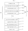
- FIG. 1 illustrates a structural schematic diagram of an organic light emitting device according to an embodiment of the application.
- the organic light emitting device comprises an anode layer 1, a light emitting layer 3, a carrier velocity adjustment layer 10 and a cathode layer 2.
- the carrier velocity adjustment layer 10 of the embodiment comprises at least an elec tron velocity adjustment layer 4'.
- the electron velocity adjustment layer 4' comprises a plurality of electron trap units 40 which are provided successively, and each of the electron trap units 40 comprises an electron injection sublayer 42 and a deceleration layer 41 which are sequentially provided in a direction away from the cathode layer 2.
- the electron injection sublayer 42 is used for injecting the electrons into the deceleration layer 41, and the deceleration layer 41 is used for reducing the injection rate of the electrons.
- the electrons injected from the cathode layer 2 pass through the first electron injection sublayer 42 first, an injection capability of the electron itself is poor, and the electron injection sublayer 42 facilitates injection of the electrons. Then, the electrons pass through the first deceleration layer 41, and the injection rate of the electrons is reduced. After wards, the electrons pass through the repeated electron injection sublayer 42 and deceleration layer 41.
- Each group of the electron injection sublayer 42 and the deceleration layer 41 substantially corresponds to the electron trap unit 40 for reducing the injection rate of the electrons.
- the number of the electron trap units 40 is adjusted such that the injection rate of the electrons and the injection rate of the holes injected from the anode layer 1 tend to be balanced, and the electrons and the holes are recombined to emit light in the light emitting layer 3 at this point.
- the technical solution of the embodiment facilitates improvement of the luminous efficiency and the life time of the organic light emitting device.
- the carrier velocity adjust ment layer 10 of the embodiment further comprises an electron transport layer 5 pr ovided between the light emitting layer 3 and the electron velocity adjustment layer 4'.
- the electron transport layer 5 facilitates transport of the electrons to the light emitting layer 3.
- the organic light emitting device of the embodiment further comprises a hole injection layer 6 and a hole transport layer 7 which are provided between the anode layer 1 and the light emitting layer 3.
- the hole injection layer 6 is provided between the anode layer 1 and the hole transport layer 7.
- the hole injection layer 6 facilitates improvement of the inject ion capability of the holes
- the hole transport layer 7 facilitates improvement of the transport capability of the holes to the light emitting layer 3.
- the method of fabricating the organic light emitting device of the embodiment comprises the following steps S1 to S8.
- Step S1 comprises sputtering an anode conductive film on a substrate, and forming a pattern comprising the anode layer 1 by a patterning process.
- the substrate serves as a support for electrode layers and organic function film layers in the organic light emitting device, has a good light transmission property in the visible light region, a certain capability of preventing water vapor and oxygen permeation, and a good surface smoothness, and may be generally formed from glass, a flexible subs trate or an array substrate. If the flexible substrate is selected, the substrate may be made of polyester, polyphthalimide or thin metal.
- the anode layer 1 serves as a connection layer for a positive voltage in the organic light emitting device, and has a good conductivity, a light transmission property in the visible light region and a high work function.
- the anode layer 1 may be made of an inorganic metal oxide (e.g., indium tin oxide (ITO), zinc oxide (ZnO), etc.), an organic conductive polymer (e.g., poly(3,4-ethylenedioxythiophene): polystyrene sulfonate (PEDOT :PSS), polyaniline (PANI), et c.) or a metal material with high work function on (e.g., gold, copper, silver, platinum, etc.).
- the thickness of the anode layer 1 may range from 10nm to 200nm.
- Step S2 comprises forming, by using a vacuum evaporation process, the hole injection layer 6 on the substrate having the anode layer 1 formed thereon.
- the mate rial of the hole injection layer 6 may comprise any one of 2,3,6,7,10,1 1-hexacyano-1,4,5,8,9,12-hexaazatriphenylene (HAT-CN), 2,3,5,6-tetrafluoro-7,7',8,8'-tetracyanoquinodimethane (F 4 -TCNQ), and tris(4-bromophenyl)aminium hexachloroantimonate (TBAHA).
- the thickness of the hole injection layer 6 may range from 1nm to 5nm.
- Step S3 comprises forming, by using a vacuum evaporation process, the hole transport layer 7 on the substrate having the hole injection layer 6 formed thereon.
- the hole transport layer 7 may comprise the material having a hole mobility larger than 10 -5 cm 2 /VS, and may be made of aromatic diamine compound, triphenylamine compound, aromatic triami ne compound, biphenyl diamine derivatives, triarylamine polymer, metal complex, or carbazole-based polymer, for example, any one of N,N'-bis(1-naphthyl)-N,N'-diphenyl-1,1'-biphenyl-4,4'-diamine (NPB), triphenyldiamine derivative (TPD), TPTE, and 1,3,5-tris(N-3-methylphenyl-N-phenylamino) benzene (TDAB).
- the thickness of the hole transport layer 7 may range from 10nm to 200nm.
- Step S4 comprises forming, by using a vacuum evaporation process, the light emitting layer 3 on the substrate having the hole transport layer 7 formed thereon.
- the light emitting layer 3 may be made of a non-doped fluorescent organic material consisting of a luminescent mate rial having a hole transport capability not lower than an electron transport capability, or may be made of a fluorescent material-doped organic material consisting of a fluorescent dopant and a host material, or may be ma de of a phosphorescent material-doped organic material consisting of a phosphorescent dopant and a host material.
- the thickness of the light emitting layer 3 may range from 10nm to 50nm.
- Step S5 comprises forming, by using a vacuum evaporation process, the electron transport layer 5 on the substrate having the light emitting layer 3 formed thereon.
- the electron transport layer 5 may comprise the material having an electron mobility larger than 10 -3 cm 2 /VS.
- the material of the electron transport layer 5 may comprise any one of 2-(4-biphenyl)-5-phenyl oxadiazole (PBD), 2,5-bis(1-naphthyl)-1,3,4-oxadiazole (BND), and 2,4,6-triphenyl-1,3,5-triazine (TRZ).
- PBD 2-(4-biphenyl)-5-phenyl oxadiazole
- BND 2,5-bis(1-naphthyl)-1,3,4-oxadiazole
- TRZ 2,4,6-triphenyl-1,3,5-triazine
- the thickness of the electron transport layer 5 may range from 10nm to 30nm.
- Step S6 comprises forming, by using a vacuum evaporation process, the first deceleration layer 41 on the substrate havi ng the electron transport layer 5 formed thereon.
- the ma terial of the deceleration layer 41 may comprise any one of magnesium (Mg), silver (Ag), aluminum (Al), lithium (Li), potassium (K) and calcium (Ca), or an alloy thereof.
- the thickness of the deceleration layer 41 may range from 1nm to 10nm.
- Step S7 comprises forming, by using a vacuum evaporation process, the first electron injection sublayer 42 on the substr ate having the first deceleration layer 41 formed thereon.
- the material of the electron injection sublayer 42 may comprise any one of lithium fluoride, sodium fluoride, potassium fluoride, rubidium fluoride, cesium fluoride, lithium oxide, and lithium metaborate.
- the thickness of the electron injection sublayer 42 may range from 1nm to 5nm.
- steps S6 and S7 are repeated, i.e., the plurality of electron trap units 40 are formed.
- the number of the electron trap units 40 may range from two to ten, e.g., may be three. Of course, the number may be set according to a specific situation.
- Step S8 comprises forming, by using a vacuum evaporation process, the cathode layer 2 on the substrate having the N-th electron injection sublayer 42 formed thereon.
- the cathode layer 2 serves as a connection layer for a negative voltage in the organic light emitting device, and has a good conductivity and a low work function.
- the cathode layer 2 may be generally made of a metal material with low work function, e.g., lithium, magnesium, calcium, strontium, aluminum, indium, etc., or an alloy of the above meta 1 with copper, gold or silver, or may be formed of a thin layer of bu ffer insulation layer (e.g., lithium fluoride LiF, cesium carbonate CsCO 3 , etc.) and the above metal or alloy.
- the thickness of the cathode layer 2 may range from 10nm to 20nm.
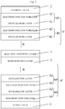
- FIG. 2 illustrates a structural schematic diagram of an organic light emitting device according to an embodiment of the application.
- the organic light emitting device comprises a substrate, and an anode layer 1, a carrier velocity adjustment layer 10, a light emitting layer 3 and a cathode layer 2 which are sequentially provided on the substrate.
- the carrier velocity adjustment layer 10 of the embodiment comprises a hole velocity adjustment layer 6'.
- the hole velocity adjustment layer 6' comprises a plurality of hole acceleration units 60 which are provided successively, and each of the hole acceleration units 60 comprise sa hole injection sublayer 61 and an acceleration layer 61 sequentially provided in a direction away from the anode layer 1.
- the hole injection sublayer 61 is used fo r injecting the holes into the acceleration layer 62, and the acceleration layer 62 is used for increasing the injection rate of the holes.
- the carrier velocity adjustment layer 10 can increase the injection rate of the holes.
- the carrier velocity adjustment layer 10 comprises the hole velocity adjustment layer 6' that consists of the plurality of hole acceleration units 60.
- the holes injected from the anode layer 1 into the light emitting layer 3 pass through one hole acceleration unit 60, and the injection rate of the holes is increased.
- Th e number of the hole acceleration units 60 is adjusted such that the injection rate of the electrons and the injection rate of the holes tend to be balanced, and the electrons and the holes are recombined to emit light in the light emitting layer 3 at this point.
- the technical solution of the embodiment facilitates improvement of the lu minous efficiency and the life time of the organic light emitting device.
- the organic light emitting device of the embodiment further comprises an electron injection layer 4 a nd an electron transport layer 5 which are provided between the cathode layer 2 and the light emitting layer 3.
- the electron transport layer 5 is provided between the light emitting layer 3 and the electron injection layer 4.
- the electron injection layer 4 and the electron transport layer 5 facilitate improvement of the capability of injecting the electrons from the cathode layer 2 into the light emitting layer 3.
- the method of fabricating the organic light emitting device of the embodiment comprises the following steps S1 to S7.
- Step S1 comprises sputtering an anode conductive film on a substrate, and forming a pattern comprising the anode layer 1 by a patterning process.
- the substrate serves as a support for electrode layers and organic function film layers in the organic light emitting device, has a good light transmission property in the visible light region, a certain capability of preventing water vapor and oxygen permeation, and a good surface smoothness, and may be generally formed from glass, a flexible substrate or an array substrate. If the flexible substrate is selected, the substrate may be made of polyester, polyphthalimide or thin metal.
- the anode layer 1 serves as a connection layer for a positive voltage in the organic light emitting device, and has a good conductivity, a light transmission property in the visible light region and a high work function.
- the anode layer 1 may be made of an inorganic metal oxide (e.g., indium tin oxide (ITO), zinc oxide (ZnO), etc.), an organic conductive polymer (e.g., poly(3,4-ethylenedioxythiophene): polystyrene sulfonate (PEDOT :PSS), polyaniline (PANI), et c.) or a metal material with high work function on (e.g., gold, copper, silver, platinum, etc.).
- the thickness of the anode layer 1 may range from 10nm to 200nm.
- Step S2 comprises forming, by using a vacuum evaporation process, the hole injection sublayer 61 of the first hole acceleration unit 60 on the substrate having the anode layer 1 formed thereon.
- the hole injection sublayer 61 may be made of an organic material or polymer doped with a phosphorescent dopant (P).
- the material of the hole injection sublayer 61 may comprise any one of 2,3,6,7,10,11-hexacyano-1,4,5,8,9 ,12-hexaazatriphenylene (HAT-CN), 2,3,5,6-tetrafluoro-7,7',8,8'-tetracyanoquinodimethane (F 4 -TCNQ), and tris(4-bromophenyl)aminium hexachloroantimonate (TBAHA).
- the thickness of the hole injection sublayer 61 may range from 1nm to 5nm, e.g., may be 1nm.
- Step S3 comprises forming, by using a vacuum evaporation process, the acceleration layer 62 on the substrate having the hole injection sublayer 61 of the first hole acceleration unit 60 formed thereon.
- the acceleration layer 62 may comprise the material having a hole mobility larger than 10 -5 cm 2 /VS.
- the acceleration layer 62 may be made of aromatic diamine compound, triphenylamine compound, aromatic triami ne compound, biphenyl diamine derivatives, triarylamine polym er, metal complex, or carbazole-based polymer, for example, any one of N,N'-bis(1-naphthyl)-N,N'-diphenyl-1,1'-biphenyl-4,4'-diamine (NPB), triphenyldiamine derivative (TPD), TPTE, and 1,3,5-tris(N-3-methylphenyl-N-phenylamino) benzene (TDAB).
- the thickness of the acceleration layer 62 may range from 10nm to 200nm.
- steps S2 and S3 are repeated to form the plurality of hole acceleration units 60.
- the number of the hole acceleration units 60 may range from two to ten, e.g., may be three.
- the numb er may be set according to a specific situation, so that the injection rate of the holes and the injection rate of the electrons tend to be balanced.
- Step S4 comprises forming, by using a vacuum evaporation process, the light emitting layer 3 on the substrate having the hole velocity adjustment layer 6' formed thereon.
- the light emitting layer 3 may be made of a non-doped fluorescent organic material consisting of a luminescent mate rial having a hole transport capability not lower than an electron transport capability, or may be made of a fluorescent material-doped organic material consisting of a fluorescent dopant and a host material, or may be ma de of a phosphorescent material-doped organic material consisting of a phosphorescent dopant and a host material.
- the thickness of the light emitting layer 3 may range from 10nm to 50nm.
- Step S5 comprises forming, by using a vacuum evaporation process, the electron transport layer 5 on the substrate having the light emitting layer 3 formed thereon.
- the electron transport layer 5 may comprise the material having a high electron mobility, for example, any one of 2-(4 -biphenyl)-5-phenyl oxadiazole (PBD), 2,5-bis(1-naphthyl)-1,3,4-oxadiazole (BND), and 2,4,6-triphenyl-1,3,5-triazine (TRZ).
- PBD 2-(4 -biphenyl)-5-phenyl oxadiazole
- BND 2,5-bis(1-naphthyl)-1,3,4-oxadiazole
- TRZ 2,4,6-triphenyl-1,3,5-triazine
- the th ickness of the electron transport layer 5 may range from 10nm to 30nm.
- Step S6 comprises forming, by using a vacuum evaporation process, the electron injection layer 4 on the substrate having the electron transport layer 5 formed thereon.
- the material of the electron injection layer 4 may comprise any one of lithium fluoride, sodium fluoride, potassium fluoride, rubidium fluoride, cesium fluoride, lithium oxide, and lithium metaborate.
- the thickness of the electron injection layer 4 may range from 1nm to 5nm.
- Step S7 comprises forming, by using a vacuum evaporation process, the cathode layer 2 on the substrate having the electron injection layer 4 formed thereon.
- the cathode layer 2 serves as a connection layer for a negative voltage in the organic light emitting device, and has a good conductivity and a low work function.
- the cathode layer 2 may be generally made of a metal material with low work function, e.g., lithium, magnesium, calcium, strontium, aluminum, indium, etc., or an alloy of the above meta 1 with copper, gold or silver, or may be formed of a thin layer of bu ffer insulation layer (e.g., lithium fluoride LiF, cesium carbonate CsCO 3 , etc.) and the above metal or all oy.
- the thickness of the cathode layer 2 may range from 10nm to 20nm.
- FIG. 3 illustrates a structural schematic diagram of an organic light emitting device according to an embodiment of the application.
- the organic light emitting device comprises an anode layer 1, a hole velocity adjustment layer 6', a light emitting layer 3, an electron velocity adjustment layer 4' and a cathode layer 2.
- the hole velocity adjustment layer 6' and the electron velocity adjustment layer 4' constitute a carrier velocity adjustment layer.
- the hole velocity adjustment layer 6' comprises a plurality of hole acceleration units 60 which are provided successively, and each of the hole acceleration units 60 comprises a hole injection sublayer 61 and an acceleration layer 61 sequentially provided in a direction away from the anode layer 1.
- the hole injection sublayer 61 is used for injecting the holes into the acceleration layer 62, and the acceleration layer 62 is used for increasing the injection rate of the holes.
- the electron velocity adjustment layer 4' comp rises a plurality of electron trap units 40 which are provided su ccessively, and each of the electron trap units 40 comprises an electron injection sublayer 42 and a deceleration layer 41 sequentially provided in a direction away from the cathode layer 2.
- the electron injection sublayer 42 is used for injecting the electrons into the deceleration layer 41, and the deceleration layer 41 is used for reducing the injection rate of the electrons.
- the electrons injected from the cathode layer 2 pass through the first electron injection sublayer 42 of the electron velocity adjustment layer 4' fi rst, an injection capability of the electron itself is poor, and the electron injection sublayer 42 facilitates injection of the electrons. Then, the electrons pass through the first deceleration layer 41, and the injection rate of the electrons is reduced. Afterwards, the electrons pass through the repeated electron injection sublayer 42 and deceleration layer 41. Each group of the electron injection sublayer 42 and the deceleration layer 41 substantially corresponds to the electron trap unit 40 for reducing the injection rate of the electrons. Meanwhile, the hole velocity ad justment layer 6' consists of the plurality of hole acceleration units 60.
- the holes injected from the anode layer 1 into the light emitting layer 3 pass through the hole acceleration unit 60, a nd the injection rate of the holes is increased.
- the number of the electron trap units 40 and the number of the hole acceleration units 60 are adjusted such that the injection rate of the electrons and the injection rate of the holes tend to be ba lanced, and the electrons and the holes are recombined to emit light in the light emitti ng layer 3 at this point.
- the organic light emitting device according to the embodiment of the application has improved luminous efficiency and life time.
- the organic light emitting device of the embodiment further comprises an electron transport layer 5 pr ovided between the light emitting layer 3 and the electron velocity adjustment layer 4'.
- the electron transport layer 5 facilitates transport of the electrons to the light emitting layer 3.
- the method of fabricating the organic light emitting device of the embodiment comprises the following steps S1 to S8.
- Step S1 comprises sputtering an anode conductive film on a substrate, and forming a pattern comprising the anode layer 1 by a patterning process.
- the substrate serves as a support for electrode layers and organic function film layers in the organic light emitting device, has a good light transmission property in the visible light region, a certain capability of preventing water vapor and oxygen permeation, and a good surface smoothness, and may be generally formed from glass, a flexible substrate or an array substrate. If the flexible substrate is selected, the substrate may be made of polyester, polyphthalimide or thin metal.
- the anode layer 1 serves as a connection layer for a positive voltage in the organic light emitting device, and has a good conductivity, a light transmission property in the visible light region and a high work function.
- the anode layer 1 may be made of an inorganic metal oxide (e.g., indium tin oxide (ITO), zinc oxide (ZnO), etc.), an organic conductive polymer (e .g., poly (3,4-ethylenedioxythiophene) / polystyrene sulfonate (PEDOT :PSS), polyaniline (PANI), et c.) or a metal material with high work function on (e.g., gold, copper, silver, platinum, etc.).
- the thickness of the anode layer 1 may range from 10nm to 200nm.
- Step S2 comprises forming, by using a vacuum evaporation process, the hole injection sublayer 61 of the first hole acceleration unit 60 on the substrate having the anode layer 1 formed thereon.
- the hole injection su blayer 61 may be made of an organic material or polymer doped with a phosphorescent dopant (P).
- the hole injection sublayer 61 may be made of any one of 2,3,6,7,10,11-hexacyano-1,4,5,8,9,12-hexaazatriphenylene (HAT-CN), 2,3,5,6-tetrafluoro-7,7',8,8'-tetracyanoquinodimethane (F 4 -TCNQ), and tris(4-bromophenyl)aminium hexachloroantimonate (TBAHA).
- the thickness of the hole injection sublayer 61 may range from 1nm to 5nm, e.g., may be 1nm.
- Step S3 comprises forming, by using a vacuum evaporation process, the acceleration layer 62 on the substrate having the hole injection sublayer 61 of the first hole acceleration unit 60 formed thereon.
- the acceleration layer 62 may comprise the material having a hole transport rate larger than 10 -5 cm 2 /VS, and may be made of aromatic diamine compound, triphenylamine compound, aromatic triami ne compound, biphenyl diamine derivatives, triarylamine polym er, metal complex, or carbazole-based polymer, for example, any one of N,N'-bis(1-naphthyl)-N,N'-diphenyl-1,1'-biphenyl-4,4'-diamine (NPB), triphenyldiamine derivative (TPD), TPTE, and 1,3,5-tris(N-3-methylphenyl-N-phenylamino) benzene (TDAB).
- the thickness of the acceleration layer 62 may range from 10nm to 200nm.
- steps S2 and S3 are repeated to form the plurality of hole acceleration units 60.
- the number of the hole acceleration units 60 may range from two to ten, e.g., may be three.
- the numb er may be set according to a specific situation, so that the injection rate of the holes and the injection rate of the electrons tend to be balanced.
- Step S4 comprises forming, by using a vacuum evaporation process, the light emitting layer 3 on the substrate having the hole velocity adjustment layer 6' formed thereon.
- the light emitting layer 3 may be made of a non-doped fluorescent organic material consisting of a luminescent mate rial having a hole transport capability not lower than an electron transport capability, or may be made of a fluorescent material-doped organic material consisting of a fluorescent dopant and a host material, or may be ma de of a phosphorescent material-doped organic material consisting of a phosphorescent dopant and a host material.
- the thickness of the light emitting layer 3 may range from 10nm to 50nm.
- Step S5 comprises forming, by using a vacuum evaporation process, the electron transport layer 5 on the substrate having the light emitting layer 3 formed thereon.
- the electron transport layer 5 may comprise the material having a high electron mobility, for example, any one of 2-(4 -biphenyl)-5-phenyl oxadiazole (PBD), 2,5-bis(1-naphthyl)-1,3,4-oxadiazole (BND), and 2,4,6-triphenyl-1,3,5-triazine (TRZ).
- PBD 2-(4 -biphenyl)-5-phenyl oxadiazole
- BND 2,5-bis(1-naphthyl)-1,3,4-oxadiazole
- TRZ 2,4,6-triphenyl-1,3,5-triazine
- the th ickness of the electron transport layer 5 may range from 10nm to 30nm.
- Step S6 comprises forming, by using a vacuum evaporation process, the first deceleration layer 41 on the substrate havi ng the electron transport layer 5 formed thereon.
- the ma terial of the deceleration layer 41 may comprise any one of magnesium (Mg), silver (Ag), aluminum (Al), lithium (Li), potassium (K) and calcium (Ca), or an alloy thereof.
- the thickness of the deceleration layer 41 may range from 1nm to 10nm.
- Step S7 comprises forming, by using a vacuum evaporation process, the first electron injection sublayer 42 on the substr ate having the first deceleration layer 41 formed thereon.
- the material of the electron injection sublayer 42 may comprise any one of lithium fluoride, sodium fluoride, potassium fluoride, rubidium fluoride, cesium fluoride, lithium oxide, and lithium metaborate.
- the thickness of the electron injection sublayer 42 may range from 1nm to 5nm.
- steps S6 and S7 are repeated, i.e., the plurality of electron trap units 40 are formed.
- the number of the electron trap units 40 may be three.
- the number may be set according to a specific situation, as long as the injection rate of the electrons and the injection rate of th e holes are guaranteed to be substantially the same.
- Step S8 comprises forming, by using a vacuum evaporation process, the cathode layer 2 on the substrate havi ng the N-th electron injection sublayer 42 formed thereon.
- the cathode layer 2 serves as a connection layer for a negative voltage in the organic light emitting device, and has a good conductivity and a low work function.
- the cathode layer 2 may be generally made of a metal material with low work function, e.g., lithium, magnesium, calcium, strontium, aluminum, indium, etc., or an alloy of the above metal with copper, gold or silver, or may be formed of a thin layer of bu ffer insulation layer (e.g., lithium fluoride LiF, cesium carbonate CsCO 3 , etc.) and the above metal or all oy.
- the thickness of the cathode layer 2 may range from 10nm to 20nm.
- An embodiment of the application further provides a display device that comprises any one of the above organic light emitting devices.
- the display device of the embodiment has a good luminous efficiency and a good life time.
- the display device may be any product or component with a display function, such as an electronic paper, an OLED panel, a mobile phone, a tablet computer, a TV set, a display, a laptop, a digital photo frame, a navigator, etc.
- a display function such as an electronic paper, an OLED panel, a mobile phone, a tablet computer, a TV set, a display, a laptop, a digital photo frame, a navigator, etc.
Landscapes
- Physics & Mathematics (AREA)
- Optics & Photonics (AREA)
- Electroluminescent Light Sources (AREA)
Abstract
Description
- This application claims priority to Chinese Patent Application No.
201510542671.5, filed on August 28, 2015 - The application relates to the field of display technology, particularly to an organic light emitting device, a method of fabricating the or ganic light emitting device, and a display device.
- An organic light emitting device (referred to as OLED) is a light emitting device using an organic solid semiconductor as a light emitting material, and has a broad application prospect due to its advantages of simple fabricating process, low cost, low power consumption, high luminous brightness, wide range of operating temperature, etc.
- A structure of an existing OLED genera lly comprises an an ode layer, a cathode layer, and an organic function layer provided between the anode layer and the cathode layer. The organic function layer comprise s a hole injection layer, a hole transport layer, a light emitting layer, an electron transport layer and an electron injection layer, which are sequentially provided in a direction from the anode la yer to the cathode layer. The hole injection layer is adjacent to the anode layer, and the electron injection layer is adjacent to the cathode layer.
- A light emitting mechanism of the OLED is as follows. When an external voltage is applied between the anode layer and the cathode layer, driven by the external voltage, the holes injected from the anode layer enters the light emitting layer through the hole injection layer and the hole transport layer, and the electrons injected from the cathode layer enters the light emitting layer through the electron injection layer and the electron transport layer. The holes and the electrons which have entered the light emitting layer recombine to form exci tons in a recombination region, and the excitons emit light by radiative transition, thereby resulting in light-emitting phenomenon, i.e., electroluminescence.
- The inventor finds at least the following problems that exist in the prior art. Since the electrons and the holes have different injection rates, i.e., the injection rate of the electrons is larger than that of the hol es, amounts of the electrons and the holes injected into the recombination region of the light emitting layer are different from each other, resulting in reduction of a lumi nous efficiency and a life time of the organic light emitting device.
- In view of the above problems existing in the organic light emitting device in the prior art, the embodiments of the application provide an organic light emitting device which have a high luminous ef ficiency and a long life ti me, a method of fabricating the organic light emitting device, and a display device.
- An embodiment of the application provides an organic light emitting device comprising an anode layer, a cathode layer, and a light emitting layer provided between the anode layer and the cathode layer, the organic light emitting device further comprises a carrier velocity adjustment layer provided between the light emitting layer and at least one of the anode layer and the cathode layer, and the carrier velocity adjustment layer is used for adjusting an injection rate of a carrier.
- The carrier velocity adjustment layer may be provided between the light emitting layer and the cathode layer, and the carrier velocity adjustment layer may comprise an electron velocity adjustment layer. The electron velocity adjustment layer comprises a plurality of electron trap un its which are provided successively, and the electron trap unit comprises an electron in jection sublayer and a deceleration layer which are sequentially provided in a direction away from the cathode layer. The electron injection sublayer is used for injecting electrons into the deceleration layer, and the deceleration layer is used for reducing the injection rate of the electrons.
- The carrier velocity adjustment layer ma y further comprise an electron transport layer provided between the light emitting layer and the electron velocity adjustment layer.
- The electron transport layer may comprise a material having an electron mobility larger than 10-3cm2/VS.
- The material of the electron transport layer may comprise any one of 2-(4-biphenyl)-5-phenyl oxadiazole (PBD), 2,5-bis(1-naphthyl)-1,3,4-oxadiazole (BND), and 2,4,6-triphenyl-1,3,5-triazine (TRZ).
- A thickness of the electron transport layer may range from 10nm to 30nm.
- A material of the deceleration layer may comprise any one of magnesium, silver, aluminum, lithium, potassium and calcium, or an alloy thereof.
- A thickness of the deceleration layer may range from 1nm to 10nm.
- A material of the electron injection sublayer may comprise any one of lithium fluoride, sodium fluoride, potassium fluoride, rubidium fluoride, cesium fluoride, lithium oxide, and lithium metaborate.
- A thickness of the electron injection sublayer may range from 1nm to 5nm.
- The number of the electron trap units may range from two to ten.
- The organic light emitting device may further comprise a hole injection layer and a hole transport layer which are provided between the anode layer and the light emitting layer. The hole injection layer is provided between the anode layer and the hole transport layer.
- The carrier velocity adjustment layer may be provided between the light emitting layer and the anode layer, and the carrier velocity adjustment layer may comprise a hole velocity adjustment layer. The hole velocity adjustment layer comprises a plurality of hole acceleration units which are provided succes sively, and the hole acceleration unit comprises a hole injection sublayer and an acceleration layer sequentially provided in a direction away from the anode layer. The hole injection sublayer is used for injecting holes into the acceleration layer, and the acceleration layer is used for increasing a transport rate of the holes.
- A material of the hole injection sublayer may be a P-type doped material.
- A material of the hole injection sublayer may comprise any one of 2,3,6,7,10,11-hexacyano-1,4,5,8,9,12-hexaazatriphenylne, 2,3,5,6-tetrafluoro-7,7',8,8'-tetracyanoquinodimethane, and tris(4-bromophenyl)aminium hexachloroantimonate.
- A thickness of the hole injection sublayer may range from 1nm to 5nm.
- A material of the acceleration layer may comprise any one of N,N'-bis(1-naphthyl)-N,N'-diphenyl-1,1'-biphenyl-4,4'-diamine, triphenyldiamine derivative, and 1,3,5-tris(N-3-methylphenyl-N-phenylamino) benzene.
- A thickness of the acceleration layer may range from 10nm to 200nm.
- The number of the hole acceleration units may range from two to ten.
- The organic light emitting device may further comprise an electron injection layer and an electron transport layer which are provided between the cathode layer and the light emitting layer. The electron transport layer is provided between the light emitting layer and the electron injection layer.
- The carrier velocity adjustment layer ma y comprise a hole velocity adjustment layer and an electron velocity adjustment la yer, the hole velocity adjustment layer is provided between the anode layer and the light emitting layer, and the electron velocity adjustment layer is provided between the cathode layer and the light emitting layer. The hole velocity adjustment layer comprises a plurality of hole acceleration units which are provided successively, the hole acceleration unit comprises a hole injection sublayer and an acceleration layer sequentially provided in a direction away from the anode layer, the hole injection sublayer is used for injecting holes into the acceleration layer, and the acceleration layer is used for increasing a transport rate of the holes. The electron velocity adjustment layer comprises a plurality of electron trap units which are provided successively, the electron trap unit comprises an electron injection sublayer and a deceleration layer which are sequentially provided in a direction away from the cathode layer, the electron injection sublayer is used for injecting electrons into the deceleration layer, and the deceleration layer is used for reducing the injection rate of the electrons.
- The organic light emitting device may further comprise an electron transport layer provided between the light emitting layer and the electron velocity adjustment layer.
- An embodiment of the application further provides a method of fabricating an organic light emitting device, comprising forming an anode layer and a cathode layer on a substrate, and forming a light emitting layer between the cathode layer and the anode layer, and the method further comprises forming a ca rrier velocity adjustment layer between the light emitting layer and at least one of the anode layer and the cathode layer,
- The carrier velocity adjustment layer may be formed between the cathode layer and the light emitting layer, and the carrier velocity adjustment layer comprises an electron velocity adjustment layer. The electron velocity adjustment layer comprises a plurality of electron trap units which are provided successively, and the electron trap unit comprises an electron injection sublayer and a deceleration layer which are sequentially provided in a direction away from the cathode layer. The electron injection sublayer is used fo r injecting electrons into the deceleration layer, and the deceleration layer is used for reducing the injection rate of the electrons. Forming the electron velocity adjustment layer comprises: sequentially forming, by using an evaporation process, the deceleration layer and the electron injection sublayer on the substrate having the light emitting layer formed thereon; and then repeatedly forming the deceleration layer and the electron injection sublayer.
- Forming the electron velocity adjustment layer may further comprise forming an electron transport layer between the light emitting layer and th e deceleration layer closest to the light emitting layer.
- The carrier velocity adjustment layer ma y be formed between the light emitting layer and the anode layer, and the carrier velocity adjustment layer comprises a hole velocity adjustment layer. The hole velocity adjustment layer comprises a plurality of hole acceleration units which are provided successively, and the hole acceleration unit comprises a hole injection sublayer and an acceleration layer sequentially provided in a direction away from the anode layer. The hole injection sublayer is used for injecting holes into the acceleration layer, and the acceleration layer is used for increasing a transport rate of the holes. Forming the hole velocity adjustment layer comprises: sequentially forming, by using an evaporation process, the hole injection sublayer and the acceleration layer on th e substrate having the anode layer formed thereon; and then repeatedly forming the hole injection sublayer and the acceleration layer.
- The carrier velocity adjustment layer ma y comprise a hole velocity adjustment layer and an electron velocity adjustment la yer, the hole velocity adjustment layer is formed between the anode layer and the light emitting layer, and the electron velocity adjustment layer is formed between the cathode layer and the light emitting layer. The hole velocity adjustment layer comprise s a plurality of hole acceleration units which are provided successively, the hole acceleration unit comprises a hole injection sublayer and an acceleration layer sequentially provided in a direction away from the anode layer, the hole injection sublayer is used for injecting holes into the acceleration layer, and the acceleration layer is used for increasing a transport rate of the holes. The electron velocity adjustment layer comprises a plurality of electron trap units which are provided successively, the electron trap unit comprises an electron injection sublayer and a deceleration layer which are sequentially provided in a direction away from the cathode layer, the electron injection sublayer is used for injecting electrons into the deceleration layer, and the deceleration layer is used for reducing the injection rate of the electrons. Forming the hole velocity adjustment layer comprises: sequentially forming, by using an evaporation process, the hole injection sublayer and the acceleration layer on the substrate having the anode layer formed thereon; and then repeatedly form ing the hole injection sublayer and the acceleration layer. Forming the electron velocity adjustment layer comprises: sequentially forming, by using an evaporation process, the deceleration layer and the electron injection sublayer on the substrate having the light emitting layer formed thereon; and then repeatedly forming the deceleration layer and the electron injection sublayer.
- Forming the electron velocity adjustment layer may further comprise forming an electron transport layer between the light emitting layer and the deceleration layer closest to the light emitting layer.
- An embodiment of the application further provides a display device, comprising the organic light emitting device described above.
- The carrier velocity adjustment layer is provided in the organic light emitting device of the embodiments of the applicat ion, and the carrier velocity adjustment layer is provided between the light emitting layer and at least one of the anode layer and the cathode layer. The carrier velocity adjustment layer may adjust the injection rate of corresponding carrier into the light emitting layer, so that the injection rates of different carriers tend to be balanced, thereby improving the luminous efficiency and the life time of the organic light emitting device.
-
-
FIG. 1 is a structural schematic diagram of an organic light emitting device according to an embodiment of the application. -
FIG. 2 is a structural schematic diagram of an organic light emitting device according to an embodiment of the application. -
FIG. 3 is a structural schematic diagram of an organic light emitting device according to an embodiment of the application. - To make the persons skilled in the art better understand the technical solutions of the application, the application will be described in detail below, in conjunction with drawings and specific embodiments.
- An embodiment of the ap plication provides an organic light emitting device, comprising an anode layer, a cathode layer, and a light emitting layer provided between the anode layer and the cathode layer. The organic light emitting device further comprises a carrier velocity adjustment layer that is provided between the light emitting layer and at least one of the anode layer and the cathode layer. The carrier velocity adjustment layer is used for adjusting an injection rate of a carrier.
- In the existing organic light emitting device, when the organic light emitting device is driven to emit light, since the injection rate of the holes injected from the anode layer to the light emitting layer is diff erent from that of the electrons injected from the cathode layer to the light emitting layer, i.e., the injection rate of the holes is smaller than that of the electrons, amounts of the electrons and the holes injected into the recombination region of the light emitting layer at the same time are different from each other, thus resulting in reduction of the luminous efficiency and the life time of the organic light emitting device.
- In the organic light emitting device of the embodiment, the carrier velocity adjustment layer is added, and is provided between th e light emitting layer and at least one of the anode layer and the cathode layer. The carrier velocity adjustment layer may adjust the injection rate of corresponding carrier into the light emitting layer, so that the injection rates of different carriers tend to be balanced, thus improving the luminous efficiency and the life time of the organic light emitting device.
- Specifically,
FIG. 1 illustrates a structural schematic diagram of an organic light emitting device according to an embodiment of the application. The organic light emitting device comprises ananode layer 1, alight emitting layer 3, a carriervelocity adjustment layer 10 and acathode layer 2. The carriervelocity adjustment layer 10 of the embodiment comprises at least an elec tron velocity adjustment layer 4'. The electron velocity adjustment layer 4' comprises a plurality ofelectron trap units 40 which are provided successively, and each of theelectron trap units 40 comprises anelectron injection sublayer 42 and adeceleration layer 41 which are sequentially provided in a direction away from thecathode layer 2. Theelectron injection sublayer 42 is used for injecting the electrons into thedeceleration layer 41, and thedeceleration layer 41 is used for reducing the injection rate of the electrons. - When an external voltage is applied to the organic light emitting device, the electrons injected from the
cathode layer 2 pass through the firstelectron injection sublayer 42 first, an injection capability of the electron itself is poor, and theelectron injection sublayer 42 facilitates injection of the electrons. Then, the electrons pass through thefirst deceleration layer 41, and the injection rate of the electrons is reduced. After wards, the electrons pass through the repeatedelectron injection sublayer 42 anddeceleration layer 41. Each group of theelectron injection sublayer 42 and thedeceleration layer 41 substantially corresponds to theelectron trap unit 40 for reducing the injection rate of the electrons. The number of theelectron trap units 40 is adjusted such that the injection rate of the electrons and the injection rate of the holes injected from theanode layer 1 tend to be balanced, and the electrons and the holes are recombined to emit light in thelight emitting layer 3 at this point. The technical solution of the embodiment facilitates improvement of the luminous efficiency and the life time of the organic light emitting device. - For example, the carrier velocity adjust
ment layer 10 of the embodiment further comprises anelectron transport layer 5 pr ovided between the light emittinglayer 3 and the electron velocity adjustment layer 4'. Theelectron transport layer 5 facilitates transport of the electrons to thelight emitting layer 3. - For example, the organic light emitting device of the embodiment further comprises a
hole injection layer 6 and ahole transport layer 7 which are provided between theanode layer 1 and thelight emitting layer 3. Thehole injection layer 6 is provided between theanode layer 1 and thehole transport layer 7. Thehole injection layer 6 facilitates improvement of the inject ion capability of the holes, and thehole transport layer 7 facilitates improvement of the transport capability of the holes to thelight emitting layer 3. - Materials and thicknesses of the layers of the above organic light emitting device are described in detail in conjunction with a method of fabricating the organic light emitting device described below.
- The method of fabricating the organic light emitting device of the embodiment comprises the following steps S1 to S8.
- Step S1 comprises sputtering an anode conductive film on a substrate, and forming a pattern comprising the
anode layer 1 by a patterning process. - In this embodiment, the substrate serves as a support for electrode layers and organic function film layers in the organic light emitting device, has a good light transmission property in the visible light region, a certain capability of preventing water vapor and oxygen permeation, and a good surface smoothness, and may be generally formed from glass, a flexible subs trate or an array substrate. If the flexible substrate is selected, the substrate may be made of polyester, polyphthalimide or thin metal.
- In addition, the
anode layer 1 serves as a connection layer for a positive voltage in the organic light emitting device, and has a good conductivity, a light transmission property in the visible light region and a high work function. Theanode layer 1 may be made of an inorganic metal oxide (e.g., indium tin oxide (ITO), zinc oxide (ZnO), etc.), an organic conductive polymer (e.g., poly(3,4-ethylenedioxythiophene): polystyrene sulfonate (PEDOT :PSS), polyaniline (PANI), et c.) or a metal material with high work functi on (e.g., gold, copper, silver, platinum, etc.). The thickness of theanode layer 1 may range from 10nm to 200nm. - Step S2 comprises forming, by using a vacuum evaporation process, the
hole injection layer 6 on the substrate having theanode layer 1 formed thereon. - In this embodiment, the mate rial of the
hole injection layer 6 may comprise any one of 2,3,6,7,10,1 1-hexacyano-1,4,5,8,9,12-hexaazatriphenylene (HAT-CN), 2,3,5,6-tetrafluoro-7,7',8,8'-tetracyanoquinodimethane (F4-TCNQ), and tris(4-bromophenyl)aminium hexachloroantimonate (TBAHA). The thickness of thehole injection layer 6 may range from 1nm to 5nm. - Step S3 comprises forming, by using a vacuum evaporation process, the
hole transport layer 7 on the substrate having thehole injection layer 6 formed thereon. - In this embodiment, the
hole transport layer 7 may comprise the material having a hole mobility larger than 10 -5cm2/VS, and may be made of aromatic diamine compound, triphenylamine compound, aromatic triami ne compound, biphenyl diamine derivatives, triarylamine polymer, metal complex, or carbazole-based polymer, for example, any one of N,N'-bis(1-naphthyl)-N,N'-diphenyl-1,1'-biphenyl-4,4'-diamine (NPB), triphenyldiamine derivative (TPD), TPTE, and 1,3,5-tris(N-3-methylphenyl-N-phenylamino) benzene (TDAB). The thickness of thehole transport layer 7 may range from 10nm to 200nm. - Step S4 comprises forming, by using a vacuum evaporation process, the
light emitting layer 3 on the substrate having thehole transport layer 7 formed thereon. - In this embodiment, the
light emitting layer 3 may be made of a non-doped fluorescent organic material consisting of a luminescent mate rial having a hole transport capability not lower than an electron transport capability, or may be made of a fluorescent material-doped organic material consisting of a fluorescent dopant and a host material, or may be ma de of a phosphorescent material-doped organic material consisting of a phosphorescent dopant and a host material. The thickness of thelight emitting layer 3 may range from 10nm to 50nm. - Step S5 comprises forming, by using a vacuum evaporation process, the
electron transport layer 5 on the substrate having thelight emitting layer 3 formed thereon. - In this embodiment, the
electron transport layer 5 may comprise the material having an electron mobility larger than 10-3cm2/VS. - For example, the material of the
electron transport layer 5 may comprise any one of 2-(4-biphenyl)-5-phenyl oxadiazole (PBD), 2,5-bis(1-naphthyl)-1,3,4-oxadiazole (BND), and 2,4,6-triphenyl-1,3,5-triazine (TRZ). - For example, the thickness of the
electron transport layer 5 may range from 10nm to 30nm. - Step S6 comprises forming, by using a vacuum evaporation process, the
first deceleration layer 41 on the substrate havi ng theelectron transport layer 5 formed thereon. - In this embodiment, the ma terial of the
deceleration layer 41 may comprise any one of magnesium (Mg), silver (Ag), aluminum (Al), lithium (Li), potassium (K) and calcium (Ca), or an alloy thereof. The thickness of thedeceleration layer 41 may range from 1nm to 10nm. - Step S7 comprises forming, by using a vacuum evaporation process, the first
electron injection sublayer 42 on the substr ate having thefirst deceleration layer 41 formed thereon. - In this embodiment, the material of the
electron injection sublayer 42 may comprise any one of lithium fluoride, sodium fluoride, potassium fluoride, rubidium fluoride, cesium fluoride, lithium oxide, and lithium metaborate. The thickness of theelectron injection sublayer 42 may range from 1nm to 5nm. - Then, steps S6 and S7 are repeated, i.e., the plurality of
electron trap units 40 are formed. The number of theelectron trap units 40 may range from two to ten, e.g., may be three. Of course, the number may be set according to a specific situation. - Step S8 comprises forming, by using a vacuum evaporation process, the
cathode layer 2 on the substrate having the N-thelectron injection sublayer 42 formed thereon. - In this embodiment, the
cathode layer 2 serves as a connection layer for a negative voltage in the organic light emitting device, and has a good conductivity and a low work function. Thecathode layer 2 may be generally made of a metal material with low work function, e.g., lithium, magnesium, calcium, strontium, aluminum, indium, etc., or an alloy of theabove meta 1 with copper, gold or silver, or may be formed of a thin layer of bu ffer insulation layer (e.g., lithium fluoride LiF, cesium carbonate CsCO3, etc.) and the above metal or alloy. The thickness of thecathode layer 2 may range from 10nm to 20nm. - Thus, the fabrication of the organic li ght emitting device of the embodiment is completed.
-
FIG. 2 illustrates a structural schematic diagram of an organic light emitting device according to an embodiment of the application. The organic light emitting device comprises a substrate, and ananode layer 1, a carriervelocity adjustment layer 10, alight emitting layer 3 and acathode layer 2 which are sequentially provided on the substrate. The carriervelocity adjustment layer 10 of the embodiment comprises a hole velocity adjustment layer 6'. The hole velocity adjustment layer 6' comprises a plurality ofhole acceleration units 60 which are provided successively, and each of thehole acceleration units 60 comprise sahole injection sublayer 61 and anacceleration layer 61 sequentially provided in a direction away from theanode layer 1. Thehole injection sublayer 61 is used fo r injecting the holes into theacceleration layer 62, and theacceleration layer 62 is used for increasing the injection rate of the holes. - In this embodiment, since the carrier
velocity adjustment layer 10 is provided between theanode layer 1 and thelight emitting layer 3, the carriervelocity adjustment layer 10 can increase the injection rate of the holes. Specifically, the carriervelocity adjustment layer 10 comprises the hole velocity adjustment layer 6' that consists of the plurality ofhole acceleration units 60. When an external voltage is applied to the organic light emitting device, the holes injected from theanode layer 1 into thelight emitting layer 3 pass through onehole acceleration unit 60, and the injection rate of the holes is increased. Th e number of thehole acceleration units 60 is adjusted such that the injection rate of the electrons and the injection rate of the holes tend to be balanced, and the electrons and the holes are recombined to emit light in thelight emitting layer 3 at this point. The technical solution of the embodiment facilitates improvement of the lu minous efficiency and the life time of the organic light emitting device. - For example, the organic light emitting device of the embodiment further comprises an electron injection layer 4 a nd an
electron transport layer 5 which are provided between thecathode layer 2 and thelight emitting layer 3. Theelectron transport layer 5 is provided between the light emittinglayer 3 and theelectron injection layer 4. Theelectron injection layer 4 and theelectron transport layer 5 facilitate improvement of the capability of injecting the electrons from thecathode layer 2 into thelight emitting layer 3. - Materials and thicknesses of the layers of the above organic light emitting device are described in detail in conjunction with a method of fabricating the organic light emitting device described below.
- The method of fabricating the organic light emitting device of the embodiment comprises the following steps S1 to S7.
- Step S1 comprises sputtering an anode conductive film on a substrate, and forming a pattern comprising the
anode layer 1 by a patterning process. - In this embodiment, the substrate serves as a support for electrode layers and organic function film layers in the organic light emitting device, has a good light transmission property in the visible light region, a certain capability of preventing water vapor and oxygen permeation, and a good surface smoothness, and may be generally formed from glass, a flexible substrate or an array substrate. If the flexible substrate is selected, the substrate may be made of polyester, polyphthalimide or thin metal.
- In addition, the
anode layer 1 serves as a connection layer for a positive voltage in the organic light emitting device, and has a good conductivity, a light transmission property in the visible light region and a high work function. Theanode layer 1 may be made of an inorganic metal oxide (e.g., indium tin oxide (ITO), zinc oxide (ZnO), etc.), an organic conductive polymer (e.g., poly(3,4-ethylenedioxythiophene): polystyrene sulfonate (PEDOT :PSS), polyaniline (PANI), et c.) or a metal material with high work functi on (e.g., gold, copper, silver, platinum, etc.). The thickness of theanode layer 1 may range from 10nm to 200nm. - Step S2 comprises forming, by using a vacuum evaporation process, the
hole injection sublayer 61 of the firsthole acceleration unit 60 on the substrate having theanode layer 1 formed thereon. - In this embodiment, the
hole injection sublayer 61 may be made of an organic material or polymer doped with a phosphorescent dopant (P). - For example, the material of the
hole injection sublayer 61 may comprise any one of 2,3,6,7,10,11-hexacyano-1,4,5,8,9 ,12-hexaazatriphenylene (HAT-CN), 2,3,5,6-tetrafluoro-7,7',8,8'-tetracyanoquinodimethane (F4-TCNQ), and tris(4-bromophenyl)aminium hexachloroantimonate (TBAHA). The thickness of thehole injection sublayer 61 may range from 1nm to 5nm, e.g., may be 1nm. - Step S3 comprises forming, by using a vacuum evaporation process, the
acceleration layer 62 on the substrate having thehole injection sublayer 61 of the firsthole acceleration unit 60 formed thereon. - In this embodiment, the
acceleration layer 62 may comprise the material having a hole mobility larger than 10-5cm2/VS. - Specifically, the
acceleration layer 62 may be made of aromatic diamine compound, triphenylamine compound, aromatic triami ne compound, biphenyl diamine derivatives, triarylamine polym er, metal complex, or carbazole-based polymer, for example, any one of N,N'-bis(1-naphthyl)-N,N'-diphenyl-1,1'-biphenyl-4,4'-diamine (NPB), triphenyldiamine derivative (TPD), TPTE, and 1,3,5-tris(N-3-methylphenyl-N-phenylamino) benzene (TDAB). The thickness of theacceleration layer 62 may range from 10nm to 200nm. - Then, steps S2 and S3 are repeated to form the plurality of
hole acceleration units 60. The number of thehole acceleration units 60 may range from two to ten, e.g., may be three. Of course, the numb er may be set according to a specific situation, so that the injection rate of the holes and the injection rate of the electrons tend to be balanced. - Step S4 comprises forming, by using a vacuum evaporation process, the
light emitting layer 3 on the substrate having the hole velocity adjustment layer 6' formed thereon. - In this embodiment, the
light emitting layer 3 may be made of a non-doped fluorescent organic material consisting of a luminescent mate rial having a hole transport capability not lower than an electron transport capability, or may be made of a fluorescent material-doped organic material consisting of a fluorescent dopant and a host material, or may be ma de of a phosphorescent material-doped organic material consisting of a phosphorescent dopant and a host material. The thickness of thelight emitting layer 3 may range from 10nm to 50nm. - Step S5 comprises forming, by using a vacuum evaporation process, the
electron transport layer 5 on the substrate having thelight emitting layer 3 formed thereon. - In this embodiment, the
electron transport layer 5 may comprise the material having a high electron mobility, for example, any one of 2-(4 -biphenyl)-5-phenyl oxadiazole (PBD), 2,5-bis(1-naphthyl)-1,3,4-oxadiazole (BND), and 2,4,6-triphenyl-1,3,5-triazine (TRZ). The th ickness of theelectron transport layer 5 may range from 10nm to 30nm. - Step S6 comprises forming, by using a vacuum evaporation process, the
electron injection layer 4 on the substrate having theelectron transport layer 5 formed thereon. - In this embodiment, the material of the
electron injection layer 4 may comprise any one of lithium fluoride, sodium fluoride, potassium fluoride, rubidium fluoride, cesium fluoride, lithium oxide, and lithium metaborate. The thickness of theelectron injection layer 4 may range from 1nm to 5nm. - Step S7 comprises forming, by using a vacuum evaporation process, the
cathode layer 2 on the substrate having theelectron injection layer 4 formed thereon. - In this embodiment, the
cathode layer 2 serves as a connection layer for a negative voltage in the organic light emitting device, and has a good conductivity and a low work function. Thecathode layer 2 may be generally made of a metal material with low work function, e.g., lithium, magnesium, calcium, strontium, aluminum, indium, etc., or an alloy of theabove meta 1 with copper, gold or silver, or may be formed of a thin layer of bu ffer insulation layer (e.g., lithium fluoride LiF, cesium carbonate CsCO3, etc.) and the above metal or all oy. The thickness of thecathode layer 2 may range from 10nm to 20nm. - Thus, the fabrication of the organic li ght emitting device of the embodiment is completed.
-
FIG. 3 illustrates a structural schematic diagram of an organic light emitting device according to an embodiment of the application. The organic light emitting device comprises ananode layer 1, a hole velocity adjustment layer 6', alight emitting layer 3, an electron velocity adjustment layer 4' and acathode layer 2. The hole velocity adjustment layer 6' and the electron velocity adjustment layer 4' constitute a carrier velocity adjustment layer. The hole velocity adjustment layer 6' comprises a plurality ofhole acceleration units 60 which are provided successively, and each of thehole acceleration units 60 comprises ahole injection sublayer 61 and anacceleration layer 61 sequentially provided in a direction away from theanode layer 1. Thehole injection sublayer 61 is used for injecting the holes into theacceleration layer 62, and theacceleration layer 62 is used for increasing the injection rate of the holes. The electron velocity adjustment layer 4' comp rises a plurality ofelectron trap units 40 which are provided su ccessively, and each of theelectron trap units 40 comprises anelectron injection sublayer 42 and adeceleration layer 41 sequentially provided in a direction away from thecathode layer 2. Theelectron injection sublayer 42 is used for injecting the electrons into thedeceleration layer 41, and thedeceleration layer 41 is used for reducing the injection rate of the electrons. - When an external voltage is applied to the organic light emitting device, the electrons injected from the
cathode layer 2 pass through the firstelectron injection sublayer 42 of the electron velocity adjustment layer 4' fi rst, an injection capability of the electron itself is poor, and theelectron injection sublayer 42 facilitates injection of the electrons. Then, the electrons pass through thefirst deceleration layer 41, and the injection rate of the electrons is reduced. Afterwards, the electrons pass through the repeatedelectron injection sublayer 42 anddeceleration layer 41. Each group of theelectron injection sublayer 42 and thedeceleration layer 41 substantially corresponds to theelectron trap unit 40 for reducing the injection rate of the electrons. Meanwhile, the hole velocity ad justment layer 6' consists of the plurality ofhole acceleration units 60. When an external voltage is applied to the organic light emitting device, the holes injected from theanode layer 1 into thelight emitting layer 3 pass through thehole acceleration unit 60, a nd the injection rate of the holes is increased. The number of theelectron trap units 40 and the number of thehole acceleration units 60 are adjusted such that the injection rate of the electrons and the injection rate of the holes tend to be ba lanced, and the electrons and the holes are recombined to emit light in the light emitti nglayer 3 at this point. The organic light emitting device according to the embodiment of the application has improved luminous efficiency and life time. - For example, the organic light emitting device of the embodiment further comprises an
electron transport layer 5 pr ovided between the light emittinglayer 3 and the electron velocity adjustment layer 4'. Theelectron transport layer 5 facilitates transport of the electrons to thelight emitting layer 3. - Materials and thicknesses of the layers of the above organic light emitting device are described in detail in conjunction with a method of fabricating the organic light emitting device described below.
- The method of fabricating the organic light emitting device of the embodiment comprises the following steps S1 to S8.
- Step S1 comprises sputtering an anode conductive film on a substrate, and forming a pattern comprising the
anode layer 1 by a patterning process. - In this embodiment, the substrate serves as a support for electrode layers and organic function film layers in the organic light emitting device, has a good light transmission property in the visible light region, a certain capability of preventing water vapor and oxygen permeation, and a good surface smoothness, and may be generally formed from glass, a flexible substrate or an array substrate. If the flexible substrate is selected, the substrate may be made of polyester, polyphthalimide or thin metal.
- In addition, the
anode layer 1 serves as a connection layer for a positive voltage in the organic light emitting device, and has a good conductivity, a light transmission property in the visible light region and a high work function. Theanode layer 1 may be made of an inorganic metal oxide (e.g., indium tin oxide (ITO), zinc oxide (ZnO), etc.), an organic conductive polymer (e .g., poly (3,4-ethylenedioxythiophene) / polystyrene sulfonate (PEDOT :PSS), polyaniline (PANI), et c.) or a metal material with high work functi on (e.g., gold, copper, silver, platinum, etc.). The thickness of theanode layer 1 may range from 10nm to 200nm. - Step S2 comprises forming, by using a vacuum evaporation process, the
hole injection sublayer 61 of the firsthole acceleration unit 60 on the substrate having theanode layer 1 formed thereon. - In this embodiment, the hole injection su blayer 61 may be made of an organic material or polymer doped with a phosphorescent dopant (P). For example, the
hole injection sublayer 61 may be made of any one of 2,3,6,7,10,11-hexacyano-1,4,5,8,9,12-hexaazatriphenylene (HAT-CN), 2,3,5,6-tetrafluoro-7,7',8,8'-tetracyanoquinodimethane (F4-TCNQ), and tris(4-bromophenyl)aminium hexachloroantimonate (TBAHA). The thickness of thehole injection sublayer 61 may range from 1nm to 5nm, e.g., may be 1nm. - Step S3 comprises forming, by using a vacuum evaporation process, the
acceleration layer 62 on the substrate having thehole injection sublayer 61 of the firsthole acceleration unit 60 formed thereon. - In this embodiment, the
acceleration layer 62 may comprise the material having a hole transport rate larger than 10 -5cm2/VS, and may be made of aromatic diamine compound, triphenylamine compound, aromatic triami ne compound, biphenyl diamine derivatives, triarylamine polym er, metal complex, or carbazole-based polymer, for example, any one of N,N'-bis(1-naphthyl)-N,N'-diphenyl-1,1'-biphenyl-4,4'-diamine (NPB), triphenyldiamine derivative (TPD), TPTE, and 1,3,5-tris(N-3-methylphenyl-N-phenylamino) benzene (TDAB). The thickness of theacceleration layer 62 may range from 10nm to 200nm. - Then, steps S2 and S3 are repeated to form the plurality of
hole acceleration units 60. The number of thehole acceleration units 60 may range from two to ten, e.g., may be three. Of course, the numb er may be set according to a specific situation, so that the injection rate of the holes and the injection rate of the electrons tend to be balanced. - Step S4 comprises forming, by using a vacuum evaporation process, the
light emitting layer 3 on the substrate having the hole velocity adjustment layer 6' formed thereon. - In this embodiment, the
light emitting layer 3 may be made of a non-doped fluorescent organic material consisting of a luminescent mate rial having a hole transport capability not lower than an electron transport capability, or may be made of a fluorescent material-doped organic material consisting of a fluorescent dopant and a host material, or may be ma de of a phosphorescent material-doped organic material consisting of a phosphorescent dopant and a host material. The thickness of thelight emitting layer 3 may range from 10nm to 50nm. - Step S5 comprises forming, by using a vacuum evaporation process, the
electron transport layer 5 on the substrate having thelight emitting layer 3 formed thereon. - In this embodiment, the
electron transport layer 5 may comprise the material having a high electron mobility, for example, any one of 2-(4 -biphenyl)-5-phenyl oxadiazole (PBD), 2,5-bis(1-naphthyl)-1,3,4-oxadiazole (BND), and 2,4,6-triphenyl-1,3,5-triazine (TRZ). The th ickness of theelectron transport layer 5 may range from 10nm to 30nm. - Step S6 comprises forming, by using a vacuum evaporation process, the
first deceleration layer 41 on the substrate havi ng theelectron transport layer 5 formed thereon. - In this embodiment, the ma terial of the
deceleration layer 41 may comprise any one of magnesium (Mg), silver (Ag), aluminum (Al), lithium (Li), potassium (K) and calcium (Ca), or an alloy thereof. The thickness of thedeceleration layer 41 may range from 1nm to 10nm. - Step S7 comprises forming, by using a vacuum evaporation process, the first
electron injection sublayer 42 on the substr ate having thefirst deceleration layer 41 formed thereon. - In this embodiment, the material of the
electron injection sublayer 42 may comprise any one of lithium fluoride, sodium fluoride, potassium fluoride, rubidium fluoride, cesium fluoride, lithium oxide, and lithium metaborate. The thickness of theelectron injection sublayer 42 may range from 1nm to 5nm. - Then, steps S6 and S7 are repeated, i.e., the plurality of
electron trap units 40 are formed. For example, the number of theelectron trap units 40 may be three. Of course, the number may be set according to a specific situation, as long as the injection rate of the electrons and the injection rate of th e holes are guaranteed to be substantially the same. - Step S8 comprises forming, by using a vacuum evaporation process, the
cathode layer 2 on the substrate havi ng the N-thelectron injection sublayer 42 formed thereon. - In this embodiment, the
cathode layer 2 serves as a connection layer for a negative voltage in the organic light emitting device, and has a good conductivity and a low work function. Thecathode layer 2 may be generally made of a metal material with low work function, e.g., lithium, magnesium, calcium, strontium, aluminum, indium, etc., or an alloy of the above metal with copper, gold or silver, or may be formed of a thin layer of bu ffer insulation layer (e.g., lithium fluoride LiF, cesium carbonate CsCO3, etc.) and the above metal or all oy. The thickness of thecathode layer 2 may range from 10nm to 20nm. - Thus, the fabrication of the organic light emitting device of the embodiment is completed.
- An embodiment of the application further provides a display device that comprises any one of the above organic light emitting devices. The display device of the embodiment has a good luminous efficiency and a good life time.
- The display device may be any product or component with a display function, such as an electronic paper, an OLED panel, a mobile phone, a tablet computer, a TV set, a display, a laptop, a digital photo frame, a navigator, etc.
- It should be understood that the above embodiments are only exemplary embodiments for illustrating the principle of the application, but the application is not limited thereto. Various variations and im provements can be made by the person of ordinary skill in the art without departing from the spirit and essence of the application, and these variations and improvements should also be considered to fall within the protection scope of the application.
Claims (29)
- An organic light emitting device, comprising an anode layer, a cathode layer, and a light emitting layer provided between the anode layer and the cathode layer, wherein
the organic light emitting device further comprises a carrier velocity adjustment layer provided between the light emitting layer and at least one of the anode layer and the cathode layer, and
the carrier velocity adjustme nt layer is used for adjusting an injection rate of a carrier. - The organic light emitting device of claim 1, wherein
the carrier velocity adjustment layer is provided between the light emitting layer and the cathode layer, the carrier velocity adjustment layer comprises an electron velocity adjustment layer;
the electron velocity adjustment layer comprises a plurality of electron trap units which are provided successively, and the electron trap unit comprises an electron injection sublayer and a deceleration layer which are sequentially provided in a direction away from the cathode layer; and
the electron injection sublayer is used for injecting electrons into the deceleration layer, and the deceleration layer is used for reducing the injection rate of the electrons. - The organic light emitting device of claim 2, wherein the carrier velocity adjustment layer further comprises an electron transport layer provided between the light emitting layer and the electron velocity adjustment layer.
- The organic light emitting device of claim 3, wherein the electron transport layer comprises a material having an electron mobility larger than 10-3cm2/VS.
- The organic light emitting device of claim 4, wherein the material of the electron transport layer comprises anyone of 2-(4-biphenyl)-5-phenyl oxadiazole, 2,5-bis(1-naphthyl)-1,3,4-oxadiazole, and 2,4,6-triphenyl-1,3,5-triazine.
- The organic light emitting device of claim 3, wherein a thickness of the electron transport layer ranges from 10nm to 30nm.
- The organic light emitting device of claim 2, wherein a material of the deceleration layer comprises any one of magnesium, silver, aluminum, lithium, potassium and calcium, or an alloy thereof.
- The organic light emitting device of claim 2, wherein a thickness of the deceleration layer ranges from 1nm to 10nm.
- The organic light emitting device of claim 2, wherein a material of the electron injection sublayer comprises any one of lithium fluoride, sodium fluoride, potassium fluoride, rubidium fluoride, cesium fluoride, lithium oxide, and lithium metaborate.
- The organic light emitting device of claim 2, wherein a thickness of the electron injection sublayer ranges from 1nm to 5nm.
- The organic light emitting device of claim 2, wherein the number of the electron trap units ranges from two to ten.
- The organic light emitting device of anyone of claims 2 to 11, further comprising a hole injection layer and a hole transport layer which are provided between the anode layer and the light emitting layer, wherein
the hole injection layer is provided between the anode layer and the hole transport layer. - The organic light emitting device of claim 1, wherein
the carrier velocity adjustment layer is provided between the light emitting layer and the anode layer, the carrier velocity adjustment layer comprises a hole velocity adjustment layer;
the hole velocity adjustment layer comprises a plurality of hole acceleration units which are provided successively, and th e hole acceleration unit comprises a hole injection sublayer and an acceleration layer sequentially provided in a direction away from the anode layer; and
the hole injection sublayer is used for injecting holes into the acceleration layer, and the acceleration layer is used for increasing a transport rate of the holes. - The organic light emitting device of claim 13, wherein a material of the hole injection sublayer is a P-type doped material.
- The organic light emitting device of claim 14, wherein a material of the hole injection sublayer comprises any one of 2,3,6,7,10,11-hexacyano-1,4,5,8,9,12-hexaazatriphenylene, 2,3,5,6-tetrafluoro-7,7',8,8'-tetracyanoquinodimethane, and tris(4-bromophenyl)aminium hexachloroantimonate.
- The organic light emitting device of claim 13, wherein a thickness of the hole injection sublayer ranges from 1nm to 5nm.
- The organic light emitting device of claim 13, wherein a material of the acceleration layer comprises anyone of N,N'-bis(1-naphthyl)-N,N'-diphenyl-1,1'-biphenyl-4,4'-diamine, triphenyldiamine derivative, and 1,3,5-tris(N-3-methylphenyl-N-phenylamino) benzene.
- The organic light emitting device of claim 13, wherein a thickness of the acceleration layer ranges from 10nm to 200nm.
- The organic light emitting device of claim 13, wherein the number of the hole acceleration units ranges from two to ten.
- The organic light emitting device of any one of cl aims 13 to 19, further comprising an electron injection layer and an electron transport layer which are provided between the cathode layer and the light emitting layer, wherein
the electron transport layer is provided between the light emitting layer and the electron injection layer. - The organic light emitting device of claim 1, wherein
the carrier velocity adjustment layer co mprises a hole velocity adjustment layer and an electron velocity adjustment layer, the hole velocity ad justment layer is provided between the anode layer and the light emitting layer, and the electron velocity adjustment layer is provided between the cathode layer and the light emitting layer;
the hole velocity adjustment layer comprises a plurality of hole acceleration units which are provided successively, the hole acceleration unit comprises a hole injection sublayer and an acceleration layer sequentially provided in a direction away from the anode layer, the hole injection sublayer is used for injecting holes into the acceleration layer, and the acceleration layer is used for increasing a transport rate of the holes;
the electron velocity adjustment layer comprises a plurality of electron trap units which are provided successively, the electron trap unit comprises an electron injection sublayer and a deceleration layer which are sequentially provided in a direction away from the cathode layer, the electron injection sublayer is used for injecting electrons into the deceleration layer, and the deceleration layer is used for reducing the injection rate of the electrons. - The organic light emitting device of cl aim 21, further comprising an electron transport layer provided between the light emitting layer and the electron velocity adjustment layer.
- A method of fabricating an organic light emitting device, comprising forming an anode layer and a cathode layer on a su bstrate, and forming a light emitting layer between the cathode layer and the anode layer,
wherein the method further comprises forming a carrier velocity adjustment layer between the light emitting layer and at least one of the anode layer and the cathode layer, - The method of claim 23, wherein
the carrier velocity adjustment layer is formed between the cathode layer and the light emitting layer, the carrier velocity adjustment layer comprises an electron velocity adjustment layer;
the electron velocity adjustment layer comprises a plurality of electron trap units which are provided successively, and the electron trap unit comprises an electron injection sublayer and a deceleration layer which are sequentially provided in a direction away from the cathode layer;
the electron injection sublayer is used for injecting electrons into the deceleration layer, and the deceleration layer is used for reducing the injection rate of the electrons; and
forming the electron velocity adjustment layer comprises: sequentially forming, by using an evaporation pro cess, the deceleration layer and the electron injection sublayer on the substrate having the light emitting layer formed thereon; and then repeatedly forming the deceleration layer and the electron injection sublayer. - The method of claim 24 , wherein forming the elect ron velocity adjustment layer further comprises forming an electron transport layer between the light emitting layer and the deceleration layer closest to the light emitting layer.
- The method of claim 23, wherein
the carrier velocity adjust ment layer is formed betw een the light emitting layer and the anode layer, the carrier velocity adjustment layer comprises a hole velocity adjustment layer;
the hole velocity adjustment layer comprises a plurality of hole acceleration units which are provided successively, and th e hole acceleration unit comprises a hole injection sublayer and an acceleration layer sequentially provided in a direction away from the anode layer;
the hole injection sublayer is used for injecting holes into the acceleration layer, and the acceleration layer is used for increasing a transport rate of the holes; and
forming the hole velocity ad justment layer comprises: sequentially forming, by using an evaporation process, the hole injection sublayer and the acceleration layer on the substrate having the anode layer formed thereon; and then repeatedly forming the hole injection sublayer and the acceleration layer. - The method of claim 23, wherein
the carrier velocity adjustment layer co mprises a hole velocity adjustment layer and an electron velocity adjustment layer, the hole velocity ad justment layer is formed between the anode layer and the light emitting layer, and the electron velocity adjustment layer is formed between the cathode layer and the light emitting layer;
the hole velocity adjustment layer comprises a plurality of hole acceleration units which are provided successively, the hole acceleration unit comprises a hole injection sublayer and an acceleration layer sequentially provided in a direction away from the anode layer, the hole injection sublayer is used for injecting holes into the acceleration layer, and the acceleration layer is used for increasing a transport rate of the holes;
the electron velocity adjustment layer comprises a plurality of electron trap units which are provided successively, the electron trap unit comprises an electron injection sublayer and a deceleration layer which are sequentially provided in a direction away from the cathode layer, the electron injection sublayer is used for injecting electrons into the deceleration layer, and the deceleration layer is used for reducing the injection rate of the electrons;
forming the hole velocity ad justment layer comprises: sequentially forming, by using an evaporation process, the hole injection sublayer and the acceleration layer on the substrate having the anode layer formed thereon; and then repeatedly forming the hole injection sublayer and the acceleration layer; and
forming the electron velocity adjustment layer comprises: sequentially forming, by using an evaporation process, the deceleration layer and the electron injection sublayer on the substrate having the light emitting layer formed thereon; and then repeatedly forming the deceleration layer and the electron injection sublayer. - The method of claim 27 , wherein forming the electron velocity adjustment layer further comprises forming an electron transport layer between the light emitting layer and the deceleration layer closest to the light emitting layer.
- A display device, comprising the organic light emitting device of any one of claims 1 to 22.
Applications Claiming Priority (2)
| Application Number | Priority Date | Filing Date | Title |
|---|---|---|---|
| CN201510542671.5A CN105244446B (en) | 2015-08-28 | 2015-08-28 | Organic electroluminescence device and preparation method thereof, display device |
| PCT/CN2016/072294 WO2017036084A1 (en) | 2015-08-28 | 2016-01-27 | Organic electroluminescence component and manufacturing method thereof, and display device |
Publications (2)
| Publication Number | Publication Date |
|---|---|
| EP3343660A1 true EP3343660A1 (en) | 2018-07-04 |
| EP3343660A4 EP3343660A4 (en) | 2019-05-15 |
Family
ID=55042010
Family Applications (1)
| Application Number | Title | Priority Date | Filing Date |
|---|---|---|---|
| EP16812665.4A Withdrawn EP3343660A4 (en) | 2015-08-28 | 2016-01-27 | ORGANIC ELECTROLUMINESCENCE COMPONENT AND MANUFACTURING METHOD THEREOF, AND DISPLAY DEVICE |
Country Status (4)
| Country | Link |
|---|---|
| US (1) | US10566565B2 (en) |
| EP (1) | EP3343660A4 (en) |
| CN (1) | CN105244446B (en) |
| WO (1) | WO2017036084A1 (en) |
Families Citing this family (8)
| Publication number | Priority date | Publication date | Assignee | Title |
|---|---|---|---|---|
| CN105244446B (en) * | 2015-08-28 | 2018-06-29 | 京东方科技集团股份有限公司 | Organic electroluminescence device and preparation method thereof, display device |
| CN109427985B (en) | 2017-08-31 | 2019-12-24 | 昆山国显光电有限公司 | Organic electroluminescent device and display device |
| CN109860407A (en) * | 2019-01-31 | 2019-06-07 | 瑞声科技(南京)有限公司 | A kind of organic luminescent device and preparation method thereof |
| CN109830613A (en) * | 2019-01-31 | 2019-05-31 | 瑞声科技(南京)有限公司 | Organic luminescent device and preparation method thereof |
| CN110311045B (en) * | 2019-06-24 | 2021-02-26 | 武汉华星光电半导体显示技术有限公司 | Organic electroluminescent device |
| CN110911574A (en) | 2019-11-29 | 2020-03-24 | 昆山国显光电有限公司 | Composition, OLED device, OLED display panel and display device |
| KR102903143B1 (en) * | 2020-12-31 | 2025-12-22 | 엘지디스플레이 주식회사 | Display apparatus having a light-emitting layer |
| CN116965170B (en) * | 2022-02-23 | 2026-05-12 | 京东方科技集团股份有限公司 | Light-emitting device, preparation method thereof, display panel and display device |
Family Cites Families (28)
| Publication number | Priority date | Publication date | Assignee | Title |
|---|---|---|---|---|
| JPH03105896A (en) * | 1989-09-20 | 1991-05-02 | Hitachi Ltd | EL light emitter |
| JPH10270171A (en) * | 1997-01-27 | 1998-10-09 | Junji Kido | Organic electroluminescent device |
| JP2000196140A (en) * | 1998-12-28 | 2000-07-14 | Sharp Corp | Organic electroluminescent device and manufacturing method thereof |
| US6373186B1 (en) * | 1999-01-21 | 2002-04-16 | Tdk Corporation | Organic electroluminescent device with high resistance inorganic hole injecting layer |
| WO2000057446A1 (en) * | 1999-03-19 | 2000-09-28 | Fed Corporation | High efficiency electrodes for organic light emitting diode devices |
| WO2000065879A1 (en) * | 1999-04-28 | 2000-11-02 | Emagin Corporation | Organic electroluminescence device with high efficiency reflecting element |
| KR100596028B1 (en) * | 2001-11-12 | 2006-07-03 | 네오뷰코오롱 주식회사 | High Efficiency Organic Electroluminescent Devices |
| US6794061B2 (en) * | 2002-01-31 | 2004-09-21 | Eastman Kodak Company | Organic electroluminescent device having an adhesion-promoting layer for use with a magnesium cathode |
| US6797129B2 (en) * | 2002-06-03 | 2004-09-28 | Eastman Kodak Company | Organic light-emitting device structure using metal cathode sputtering |
| US20050069727A1 (en) * | 2003-09-30 | 2005-03-31 | Rahul Gupta | Oled emissive polymer layer |
| US6963081B2 (en) * | 2003-09-30 | 2005-11-08 | Osram Otpo Semiconductors Gmbh | Interfacial trap layer to improve carrier injection |
| JP4689176B2 (en) * | 2004-02-26 | 2011-05-25 | 大日本印刷株式会社 | Organic electroluminescence device |
| CN100403574C (en) * | 2004-04-05 | 2008-07-16 | 中山大学 | An organic electroluminescent device |
| US7126267B2 (en) * | 2004-05-28 | 2006-10-24 | Eastman Kodak Company | Tandem OLED having stable intermediate connectors |
| TWI376980B (en) * | 2006-03-14 | 2012-11-11 | Lg Chemical Ltd | Organic light emitting diode having high efficiency and process for fabricating the same |
| EP1876658A3 (en) * | 2006-07-04 | 2014-06-25 | Semiconductor Energy Laboratory Co., Ltd. | Light-emitting element, light-emitting device, and electronic device |
| US8431242B2 (en) * | 2007-10-26 | 2013-04-30 | Global Oled Technology, Llc. | OLED device with certain fluoranthene host |
| CN101159315A (en) * | 2007-11-06 | 2008-04-09 | 中国科学院长春应用化学研究所 | A kind of red organic electroluminescence device and preparation method thereof |
| CN101436646A (en) * | 2008-12-15 | 2009-05-20 | 沈阳工业大学 | Organic electroluminescent device |
| KR101320449B1 (en) | 2011-09-02 | 2013-10-23 | 주식회사 엘엠에스 | Organic electronic device |
| CN103378297B (en) * | 2012-04-25 | 2017-01-25 | 群康科技(深圳)有限公司 | Organic light emitting diode and display device including same |
| CN102881843B (en) * | 2012-09-17 | 2015-09-30 | 京东方科技集团股份有限公司 | A kind of method, light-emitting diode and luminescent device preparing Organic Light Emitting Diode |
| CN104064675A (en) * | 2013-03-21 | 2014-09-24 | 海洋王照明科技股份有限公司 | Organic electroluminescent device and preparation method thereof |
| CN104183761A (en) * | 2013-05-22 | 2014-12-03 | 海洋王照明科技股份有限公司 | Inverted organic light emission diode and preparation method thereof |
| CN104638197A (en) * | 2013-11-14 | 2015-05-20 | 海洋王照明科技股份有限公司 | Organic light-emitting device and production method thereof |
| CN103730587B (en) * | 2013-12-31 | 2017-09-29 | 北京维信诺科技有限公司 | A kind of blue light organic emissive device and OLED |
| CN104600201A (en) * | 2015-01-30 | 2015-05-06 | 京东方科技集团股份有限公司 | Organic light-emitting device, preparation method of organic light-emitting device and display device |
| CN105244446B (en) * | 2015-08-28 | 2018-06-29 | 京东方科技集团股份有限公司 | Organic electroluminescence device and preparation method thereof, display device |
-
2015
- 2015-08-28 CN CN201510542671.5A patent/CN105244446B/en active Active
-
2016
- 2016-01-27 WO PCT/CN2016/072294 patent/WO2017036084A1/en not_active Ceased
- 2016-01-27 US US15/320,130 patent/US10566565B2/en active Active
- 2016-01-27 EP EP16812665.4A patent/EP3343660A4/en not_active Withdrawn
Also Published As
| Publication number | Publication date |
|---|---|
| WO2017036084A1 (en) | 2017-03-09 |
| CN105244446A (en) | 2016-01-13 |
| US10566565B2 (en) | 2020-02-18 |
| EP3343660A4 (en) | 2019-05-15 |
| CN105244446B (en) | 2018-06-29 |
| US20170194589A1 (en) | 2017-07-06 |
Similar Documents
| Publication | Publication Date | Title |
|---|---|---|
| US10566565B2 (en) | Organic light emitting device and method of fabricating the same, and display device | |
| CN103715360B (en) | Organic electroluminescence device, display device | |
| US11737296B2 (en) | OLED display device, display panel and manufacturing method of OLED display device | |
| CN108963087A (en) | Quanta point electroluminescent device and display | |
| WO2007091548A1 (en) | Organic electroluminescent element | |
| EP2245683A1 (en) | Organic optoelectronic device and method for manufacturing the same | |
| KR101261633B1 (en) | Metal compound-metal multilayer electrodes for organic electronic devices | |
| CN108807711A (en) | A kind of OLED device and preparation method thereof, display device | |
| CN112467058A (en) | Ternary exciplex composite material main body and OLED device preparation method thereof | |
| CN102315390B (en) | Electroluminescent device and preparation method thereof | |
| CN110600619B (en) | Quantum dot light-emitting diode and preparation method thereof | |
| JP4494595B2 (en) | Organic electroluminescent device | |
| US10381591B2 (en) | Organic light emitting diode device with a photoinduced electron film layer and method for manufacturing the same | |
| US20220052303A1 (en) | Method of manufacturing perovskite light emitting device by inkjet printing | |
| US10818864B2 (en) | OLED device and manufacturing method thereof, and display apparatus | |
| CN209087913U (en) | A kind of OLED device, display device | |
| KR100983888B1 (en) | Polymer organic electroluminescent device and manufacturing method thereof | |
| US20070285002A1 (en) | Method of Improving the Charge Injection to Organic Films in Organic Thin Film Devices | |
| US12598861B2 (en) | Display panels | |
| Veera Madhava Rao et al. | Cesium carbonate as an effective interfacial layer on the high performance of polymer light-emitting devices | |
| Rao et al. | Solution processed, ionic compound dispersed with small molecular effective interfacial layer for polymer light-emitting devices | |
| KR101727746B1 (en) | Organic light emitting device and method of fabricating the same | |
| CN118284080A (en) | Light-emitting device and method for manufacturing the same, and display device | |
| CN114695706A (en) | Quantum dot light-emitting diode and preparation method thereof | |
| CN116981277A (en) | Composite materials, films, light-emitting devices and preparation methods thereof |
Legal Events
| Date | Code | Title | Description |
|---|---|---|---|
| PUAI | Public reference made under article 153(3) epc to a published international application that has entered the european phase |
Free format text: ORIGINAL CODE: 0009012 |
|
| 17P | Request for examination filed |
Effective date: 20161223 |
|
| AK | Designated contracting states |
Kind code of ref document: A1 Designated state(s): AL AT BE BG CH CY CZ DE DK EE ES FI FR GB GR HR HU IE IS IT LI LT LU LV MC MK MT NL NO PL PT RO RS SE SI SK SM TR |
|
| AX | Request for extension of the european patent |
Extension state: BA ME |
|
| DAV | Request for validation of the european patent (deleted) | ||
| DAX | Request for extension of the european patent (deleted) | ||
| A4 | Supplementary search report drawn up and despatched |
Effective date: 20190415 |
|
| RIC1 | Information provided on ipc code assigned before grant |
Ipc: H01L 51/50 20060101AFI20190409BHEP Ipc: H01L 51/54 20060101ALI20190409BHEP Ipc: H01L 51/56 20060101ALI20190409BHEP |
|
| STAA | Information on the status of an ep patent application or granted ep patent |
Free format text: STATUS: THE APPLICATION IS DEEMED TO BE WITHDRAWN |
|
| 18D | Application deemed to be withdrawn |
Effective date: 20191114 |