EP3343595A1 - Testing structure and corresponding fabrication and testing methods - Google Patents
Testing structure and corresponding fabrication and testing methods Download PDFInfo
- Publication number
- EP3343595A1 EP3343595A1 EP17208749.6A EP17208749A EP3343595A1 EP 3343595 A1 EP3343595 A1 EP 3343595A1 EP 17208749 A EP17208749 A EP 17208749A EP 3343595 A1 EP3343595 A1 EP 3343595A1
- Authority
- EP
- European Patent Office
- Prior art keywords
- contact plug
- doped epitaxial
- epitaxial region
- region
- plug
- Prior art date
- Legal status (The legal status is an assumption and is not a legal conclusion. Google has not performed a legal analysis and makes no representation as to the accuracy of the status listed.)
- Withdrawn
Links
Images


Classifications
-
- H—ELECTRICITY
- H10—SEMICONDUCTOR DEVICES; ELECTRIC SOLID-STATE DEVICES NOT OTHERWISE PROVIDED FOR
- H10P—GENERIC PROCESSES OR APPARATUS FOR THE MANUFACTURE OR TREATMENT OF DEVICES COVERED BY CLASS H10
- H10P74/00—Testing or measuring during manufacture or treatment of wafers, substrates or devices
- H10P74/20—Testing or measuring during manufacture or treatment of wafers, substrates or devices characterised by the properties tested or measured, e.g. structural or electrical properties
- H10P74/207—Electrical properties, e.g. testing or measuring of resistance, deep levels or capacitance-voltage characteristics
-
- H—ELECTRICITY
- H10—SEMICONDUCTOR DEVICES; ELECTRIC SOLID-STATE DEVICES NOT OTHERWISE PROVIDED FOR
- H10P—GENERIC PROCESSES OR APPARATUS FOR THE MANUFACTURE OR TREATMENT OF DEVICES COVERED BY CLASS H10
- H10P74/00—Testing or measuring during manufacture or treatment of wafers, substrates or devices
- H10P74/27—Structural arrangements therefor
- H10P74/277—Circuits for electrically characterising or monitoring manufacturing processes, e.g. circuits in tested chips or circuits in testing wafers
-
- G—PHYSICS
- G01—MEASURING; TESTING
- G01R—MEASURING ELECTRIC VARIABLES; MEASURING MAGNETIC VARIABLES
- G01R31/00—Arrangements for testing electric properties; Arrangements for locating electric faults; Arrangements for electrical testing characterised by what is being tested not provided for elsewhere
- G01R31/28—Testing of electronic circuits, e.g. by signal tracer
- G01R31/2851—Testing of integrated circuits [IC]
- G01R31/2886—Features relating to contacting the IC under test, e.g. probe heads; chucks
-
- H—ELECTRICITY
- H10—SEMICONDUCTOR DEVICES; ELECTRIC SOLID-STATE DEVICES NOT OTHERWISE PROVIDED FOR
- H10D—INORGANIC ELECTRIC SEMICONDUCTOR DEVICES
- H10D30/00—Field-effect transistors [FET]
- H10D30/01—Manufacture or treatment
- H10D30/021—Manufacture or treatment of FETs having insulated gates [IGFET]
- H10D30/0212—Manufacture or treatment of FETs having insulated gates [IGFET] using self-aligned silicidation
-
- H—ELECTRICITY
- H10—SEMICONDUCTOR DEVICES; ELECTRIC SOLID-STATE DEVICES NOT OTHERWISE PROVIDED FOR
- H10D—INORGANIC ELECTRIC SEMICONDUCTOR DEVICES
- H10D84/00—Integrated devices formed in or on semiconductor substrates that comprise only semiconducting layers, e.g. on Si wafers or on GaAs-on-Si wafers
- H10D84/01—Manufacture or treatment
- H10D84/0123—Integrating together multiple components covered by H10D12/00 or H10D30/00, e.g. integrating multiple IGBTs
- H10D84/0126—Integrating together multiple components covered by H10D12/00 or H10D30/00, e.g. integrating multiple IGBTs the components including insulated gates, e.g. IGFETs
- H10D84/0158—Integrating together multiple components covered by H10D12/00 or H10D30/00, e.g. integrating multiple IGBTs the components including insulated gates, e.g. IGFETs the components including FinFETs
-
- H—ELECTRICITY
- H10—SEMICONDUCTOR DEVICES; ELECTRIC SOLID-STATE DEVICES NOT OTHERWISE PROVIDED FOR
- H10D—INORGANIC ELECTRIC SEMICONDUCTOR DEVICES
- H10D84/00—Integrated devices formed in or on semiconductor substrates that comprise only semiconducting layers, e.g. on Si wafers or on GaAs-on-Si wafers
- H10D84/01—Manufacture or treatment
- H10D84/02—Manufacture or treatment characterised by using material-based technologies
- H10D84/03—Manufacture or treatment characterised by using material-based technologies using Group IV technology, e.g. silicon technology or silicon-carbide [SiC] technology
- H10D84/038—Manufacture or treatment characterised by using material-based technologies using Group IV technology, e.g. silicon technology or silicon-carbide [SiC] technology using silicon technology, e.g. SiGe
-
- H—ELECTRICITY
- H10—SEMICONDUCTOR DEVICES; ELECTRIC SOLID-STATE DEVICES NOT OTHERWISE PROVIDED FOR
- H10D—INORGANIC ELECTRIC SEMICONDUCTOR DEVICES
- H10D84/00—Integrated devices formed in or on semiconductor substrates that comprise only semiconducting layers, e.g. on Si wafers or on GaAs-on-Si wafers
- H10D84/80—Integrated devices formed in or on semiconductor substrates that comprise only semiconducting layers, e.g. on Si wafers or on GaAs-on-Si wafers characterised by the integration of at least one component covered by groups H10D12/00 or H10D30/00, e.g. integration of IGFETs
- H10D84/82—Integrated devices formed in or on semiconductor substrates that comprise only semiconducting layers, e.g. on Si wafers or on GaAs-on-Si wafers characterised by the integration of at least one component covered by groups H10D12/00 or H10D30/00, e.g. integration of IGFETs of only field-effect components
- H10D84/83—Integrated devices formed in or on semiconductor substrates that comprise only semiconducting layers, e.g. on Si wafers or on GaAs-on-Si wafers characterised by the integration of at least one component covered by groups H10D12/00 or H10D30/00, e.g. integration of IGFETs of only field-effect components of only insulated-gate FETs [IGFET]
- H10D84/834—Integrated devices formed in or on semiconductor substrates that comprise only semiconducting layers, e.g. on Si wafers or on GaAs-on-Si wafers characterised by the integration of at least one component covered by groups H10D12/00 or H10D30/00, e.g. integration of IGFETs of only field-effect components of only insulated-gate FETs [IGFET] comprising FinFETs
-
- H—ELECTRICITY
- H10—SEMICONDUCTOR DEVICES; ELECTRIC SOLID-STATE DEVICES NOT OTHERWISE PROVIDED FOR
- H10W—GENERIC PACKAGES, INTERCONNECTIONS, CONNECTORS OR OTHER CONSTRUCTIONAL DETAILS OF DEVICES COVERED BY CLASS H10
- H10W20/00—Interconnections in chips, wafers or substrates
- H10W20/01—Manufacture or treatment
- H10W20/031—Manufacture or treatment of conductive parts of the interconnections
- H10W20/0698—Local interconnections
-
- H—ELECTRICITY
- H10—SEMICONDUCTOR DEVICES; ELECTRIC SOLID-STATE DEVICES NOT OTHERWISE PROVIDED FOR
- H10W—GENERIC PACKAGES, INTERCONNECTIONS, CONNECTORS OR OTHER CONSTRUCTIONAL DETAILS OF DEVICES COVERED BY CLASS H10
- H10W20/00—Interconnections in chips, wafers or substrates
- H10W20/20—Interconnections within wafers or substrates, e.g. through-silicon vias [TSV]
-
- H—ELECTRICITY
- H10—SEMICONDUCTOR DEVICES; ELECTRIC SOLID-STATE DEVICES NOT OTHERWISE PROVIDED FOR
- H10W—GENERIC PACKAGES, INTERCONNECTIONS, CONNECTORS OR OTHER CONSTRUCTIONAL DETAILS OF DEVICES COVERED BY CLASS H10
- H10W46/00—Marks applied to devices, e.g. for alignment or identification
Definitions
- the present invention generally relates to the field of semiconductor technologies and, more particularly, relates to testing structures and their fabrication and testing methods.
- the parasitic external resistance includes the contact resistance (R c ) between the metal silicide layer and the doped source/drain regions.
- a chain mode testing structure or a Kelvin testing structure is often used to measure the contact resistance.
- the chain mode testing structure two contact plugs are connected to two ends of the metal silicide layer, respectively; and metal lines are used to connect one unit to a next unit; and all the units are connected together by a chain mode in serial.
- the resistance of the entire structure is obtained.
- the resistance is divided by the number of the contact plugs, one half of the resistance between one contact plug and the metal silicide layer is obtained. Thus, the resistance between the contact plug and the metal silicide layer is obtained.
- the chain mode testing structure is only able to obtain the contact resistance between the contact plug and the metal silicide layer, it is unable to obtain the contact resistance between the metal silicide layer and the doped source/drain regions.
- the contact resistance between the metal silicide layer and the doped source/drain regions is also an important parameter of the semiconductor device.
- a first aspect of the present invention provides a testing structure.
- the testing structure includes a base substrate, containing a well region; a first doped epitaxial region in the well region and having a doping type same as a doping type of the well region; a dielectric layer on the base substrate, and covering the well region and the first doped epitaxial region; a first contact plug passing through the dielectric layer and electrically connected with the first well region; and a second contact plug and a third contact plug, each passing through the dielectric layer and electrically connected with the first doped epitaxial region, wherein the second contact plug is independent from the third contact plug and between the first contact plug and the third contact plug.
- the testing structure further comprises: a first testing pad on a surface of a portion of the first contact plug, a second testing pad on a surface of a first end portion of the second contact plug, and a third testing pad on a surface of a second end portion of the second contact plug, and a fourth testing pad on a surface of a portion of the third contact plug.
- the second testing pad is used for applying a first external current.
- the third testing pad is used for measuring a top potential of the second contact plug.
- the first testing pad is used for applying a second external current with a value smaller than a value of the first external current.
- the fourth testing pad is used for measuring a bottom potential of the first doped epitaxial region.
- the second contact plug comprises: a metal silicide layer on the first doped epitaxial region, and a first conductive plug on the metal silicide layer.
- the metal silicide layer is on at least a portion of a surface of the first doped epitaxial region.
- the metal silicide layer is made of one or more of nickel silicide and titanium silicide.
- the first conductive plug is made of one or more of copper, aluminum and tungsten.
- the second contact plug is connected to one first doped epitaxial region adjacent to the first contact plug and the third contact plug is connected to another first doped epitaxial region.
- the testing structure further comprises: a second doped epitaxial region under the first contact plug in the well region, wherein: the first contact plug is electrically connected with the second doped epitaxial region; the second doped epitaxial region is independent from the first doped epitaxial region; and the second doped epitaxial region and the first doped epitaxial region are made of a same material.
- the first doped epitaxial region and the second doped epitaxial region are made of one of P-type doped Si and P-type doped SiGe when a doping type of the first doped epitaxial region and the second doped epitaxial region is P-type.
- the first doped epitaxial region and the second doped epitaxial region are made of one of N-type doped Si and N-type doped SiC when the doping type of the first doped epitaxial region and the second doped epitaxial region is N-type.
- the third contact plug comprises: at least a second conductive plug.
- the base substrate comprises: a semiconductor substrate; and a plurality of fins on the semiconductor substrate, wherein the well region is in the fins.
- a second aspect of the present invention includes a method for fabricating a testing structure.
- the method includes providing a base substrate containing a well region; forming a first doped epitaxial region in the well region having a doping type same as a doping type of the well region; forming a dielectric layer over the base substrate, and covering the well region and the first doped epitaxial region; forming a first contact plug passing through the dielectric layer and electrically connected with the well region at one side of the first doped epitaxial region; and forming a second contact plug and a third contact plug, each passing through the dielectric layer and electrically connected with the first doped epitaxial region, wherein the second contact plug is independent from the third contact plug and between the first contact plug and the third contact plug.
- the method according to claim 12 further comprises: forming a metal silicide layer on at least a portion of a surface of the first doped epitaxial region.
- the second contact plug is connected to one first doped epitaxial region adjacent to the first contact plug and the third contact plug is connected to another first doped epitaxial region.
- the method further comprises: forming a second doped epitaxial region under the first contact plug in the well region at one side of the first doped epitaxial region, wherein: the second doped epitaxial region is independent from the first doped epitaxial region; the second doped epitaxial region and the first doped epitaxial region are made of a same material; the first contact plug passes through the dielectric layer; and the first contact plug is electrically connected with the second doped epitaxial region.
- the third contact plug includes at least a second conductive plug.
- the well region is formed in the fins when the base substrate includes a semiconductor substrate and a plurality of fins on the semiconductor substrate.
- a third aspect of the present invention provides a testing method.
- the testing method includes providing a testing structure having a base substrate containing a well region, a first doped epitaxial region in the well region and having a doping type same as a doping type of the well region, a dielectric layer on the base substrate and covering the well region and the first doped epitaxial region, a first contact plug passing through the dielectric layer and electrically connected with the first well region; and a second contact plug and a third contact plug, each passing through the dielectric layer and electrically connected with the first doped epitaxial region, wherein the second contact plug is independent from the third contact plug and between the first contact plug and the third contact plug; applying a first external current on a first end portion of the second contact plug; applying a second external current smaller than the first external current on the first contact plug to form a current loop among the first contact plug, the first doped epitaxial region under the second contact plug and the first contact plug; measuring a top potential of the second contact plug through a second end portion
- the second external current is equal to, or smaller than zero.
- obtaining the contact resistance comprises: obtaining a total resistance by dividing a potential difference between the top potential and the bottom potential with the first external current; and obtaining a resistance of a first conductive plug of the second contact plug, a resistance of a metal silicide layer of the second contact plug and a resistance of the first doped epitaxial region, wherein a difference between the total resistance and the resistance of the first conductive plug, the resistance of the metal silicide layer and the resistance of the first doped epitaxial region is the contact resistance.
- a testing structure according to the first aspect of the present invention may be obtained by a method for fabricating a test structure according to the second aspect of the present invention.
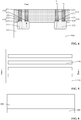
- Figure 1 illustrates a top view of the testing structure.
- Figure 2 illustrates a correlation between the total resistance measured by the testing structure illustrated in Figure 1 and the distance between adjacent contact plugs.
- TLM transmission line modeling
- the testing structure includes a base substrate (not shown); a well region (not shown) in the base substrate; a doped epitaxial region (not shown); a dielectric layer (not shown) covering the well region and the doped epitaxial region (not shown); a plurality of contact plugs passing through the dielectric layer, electrically connecting with the doped epitaxial regions and having a metal silicide layer on the doped epitaxial regions; and conductive plugs (not shown) on the metal silicide layer.
- the sizes of the plurality of contact plugs are identical and the materials of the plurality of contact plugs are identical. The distances between adjacent contact plugs are different. The widths "W" of the plurality of contact plugs are equal.
- the plurality of contact plugs includes a first contact plug CT1, a second contact plug CT2, a third contact plug CT3, a fourth contact plug CT4, a fifth contact plug CT5 and a sixth contact plug CT6.
- the distance between the first contact plug CT1 and the second contact plug CT2 is L1.
- the distance between the second contact plug CT2 and the third contact plug CT3 is L2.
- the distance between the third contact plug CT3 and the fourth contact plug CT4 is L3.
- the distance between the fourth contact plug CT4 and the fifth contact plug CT5 is L4.
- the distance between the fifth contact plug CT5 and the sixth contact plug CT6 is L5.
- L1, L2, L3, L4, and L5 are different from each other.
- the total resistance "R” between the adjacent contact plugs is obtained.
- the correlation between the total resistance “R” and the distance “L” between adjacent contact plugs is obtained by a simulation process.
- the abscissa refers to as the distance “L” between the adjacent contact plugs; and the ordinate refers to as the total resistance “R” between adjacent contact plugs.
- R c is the resistance of the contact plug.
- R SH is the sheet resistance.
- the resistance "R c " of the conductive plug includes the resistance of the conductive plug, the resistance of the metal silicide layer, and the contact resistance between the metal silicide layer and the doped epitaxial region.
- the resistance of the conductive plug and the resistance of the metal silicide layer are obtainable.
- the contact resistance between the metal silicide layer and the doped epitaxial region can be obtained by a calculation.
- the present invention provides a testing structure, a method for fabricating a testing structure, and a testing method.
- the testing structure includes a first doped epitaxial layer in the well region. The doping type of the well region and the doping type of the first doped epitaxial region may be substantially same.
- the testing structure may also include a dielectric layer; and a first contact plug, a second contact plug and a third contact plug in the dielectric layer.
- the first contact plug may be electrically connected with the well region.
- the second contact plug and the third contact plug may be electrically connected with the first doped epitaxial region.
- the second contact plug and the third plug may be independent from each other; and the second contact plug may be between the first contact plug and the third contact plug.
- a current loop may be formed among the second contact plug, the first doped epitaxial region, the well region and the first contact plug.
- the top potential of the of the second contact plug may be measured from the other end portion of the second contact plug.
- the third contact plug may be not in the current loop.
- the potential measured from the third contact plug may be the bottom potential of the first doped epitaxial region.
- the contact resistance between the metal silicide layer and the first doped epitaxial region may be obtained according to the first external current, the top potential and the bottom potential.
- TLM transmission line model
- the disclosed method may be able to avoid the errors caused by the size differences between different contact plugs.
- the contact resistance obtained by the disclosed method may have relatively high accuracy and reliability.
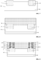
- Figures 3-4 illustrate an exemplary testing structure consistent with various disclosed embodiments.
- Figure 3 is a top view of a portion of a testing structure, where a well region and a dielectric layer are not illustrated.
- Figure 4 is a cross-sectional view of the structure illustrated in Figure 3 along the AA1 direction.
- the testing structure may include a base substrate (not labeled) and a well region 101 in the base substrate.
- the testing structure may also include a plurality of discrete first doped epitaxial regions 121 in the well region 101.
- the doping type of the first doped epitaxial regions 121 may be the same as the doping type of the well region 101.
- the testing structure may include a dielectric layer 120 on the base substrate.
- the dielectric layer 120 may cover the well region 101 and the first doped epitaxial regions 121.
- the testing structure may also include first conductive plugs 151 passing through the dielectric layer 120 and electrically connected with the well region 101; and a second contact plug 152 and a third contact plug 153 passing through the dielectric layer 120 and electrically connected with the first doped epitaxial regions 121.
- the second contact plug 152 and the third contact plug 153 may be independent from each other; and the second contact plug 152 may be between the first contact plug 151 and the third contact plug 153.
- a first testing pad 11 may be formed on a portion of the surface of the first contact plug 151.
- a second testing pad 12 and a third testing pad 13 may be formed on portions of the surface of the second contact plug 152.
- a fourth testing 14 may be formed on a portion of the surface of the third contact plug 153.
- the second contact plug 152 may include a metal silicide layer 133 on the first doped epitaxial region 121 and a first conductive plug 122 on the metal silicide layer 133.
- the second contact plug 152 may have two end portions (not labeled) along the direction parallel to the base substrate and the length direction of the second contact plug 152.
- the second testing pad 12 may be formed on one end portion, e.g., a first end portion, of the second contact plug 152; and the third testing pad 13 may be formed on the other end portion, e.g., a second end portions, of the second contact plug 152.
- the length direction of the second contact plug 152 refers to as the direction between the second testing pad 12 and the third testing pad 13.
- the base substrate includes a semiconductor substrate 100 and a plurality of discrete fins 110 on the semiconductor substrate 100.
- the well region 101 may be in the fins 110.
- the first doped epitaxial regions 121 may be formed in the fins 110.
- the semiconductor substrate 100 is a silicon substrate.
- the semiconductor substrate may also be made of germanium, silicon germanium, silicon carbide, gallium arsenide, or gallium indium, etc.
- the semiconductor substrate may also be a silicon on insulator (SOI) substrate, or a germanium on insulator (GOI) substrate.
- the fins 110 and the semiconductor substrate 100 may be made of a same material, or different materials.
- the fins 110 are made of silicon.
- the fins may be made of germanium, silicon germanium, silicon carbide, gallium arsenide, or gallium indium, etc.
- the base substrate may be a planar substrate.
- the top surface of the first doped epitaxial region 121 may be above the surface of the base substrate; and the top surface of the second doped epitaxial region 111 may be above the surface of the base substrate. That is, the top surface of the first doped epitaxial region 121 and the top surface of the second doped epitaxial region 111 may be above the top surfaces of the fins 110. In some embodiments, the top surface of the first doped epitaxial region may level the top surface of the base substrate; and the top surface of the second doped epitaxial region may level with the top surface of the base substrate.
- the cross-section of the first doped epitaxial region 121 may be square-shaped, U-shaped, or sigma-shaped, etc.
- the cross-section of the second doped epitaxial region 111 may be square-shaped, U-shaped, or sigma-shaped, etc.
- one end portion (the first end portion) of the second contact plug 152 may be used as a terminal for applying a first external current "I".
- the other end portion (the second end portion) of the second contact plug 152 may be used as a terminal for measuring the top potential "V 2 ".
- the second contact plug 152 may include the metal silicide layer 133 on the first doped epitaxial region 121 and a first conducive plug 122 on the metal silicide layer 133.
- the first metal silicide layer 133 may be made of silicon nickel, or silicon titanium, etc.
- the first conductive plug 122 may be made of Cu, Al, or W, etc.
- the metal silicide layer when the third contact plug includes the metal silicide layer on the first doped epitaxial region and the second conductive plug on the metal silicide layer, the metal silicide layer may be formed on a portion of the first doped epitaxial region; and the first conductive plug and the second conductive plug may be electrically connected to a same metal silicide layer.
- the number of the first doped epitaxial regions may be two.
- the two first doped epitaxial regions may be at a same side of the second doped epitaxial region.
- the second contact plug may be electrically connected to the first doped epitaxial region at the side adjacent to the first contact plug.
- the third contact plug may be electrically connected with the other first doped epitaxial region.
- the second conductive plug 123 and the first conductive plug 122 may be made of a same material.
- the second conductive plug 123 may be made of Cu, Al, or W, etc.
- the first contact plug 151 may be used as a terminal for applying a second external current "Com”; and the value of the second external current “Com” may be smaller than the value of the first external current "I".
- a current loop may be formed among the second contact plug 152, the first doped epitaxial region 121, the well region 101 and the first contact plug 151.
- the number of the first contact plugs 151 is two. In some embodiments, the number of the first contact plug may be one, or more than two.
- the first contact plug 151 may include the metal silicide layer 133 on the second doped epitaxial region 111 and the third conductive plug 112 on the metal silicide layer 133. In some embodiments, the first contact plug may only include a third conductive plug.
- the third conductive plug 112 may be made of a same material.
- the third conductive plug 112 may be made of Cu, Al, or W, etc.
- a current loop may be formed among the second contact plug 152, the first doped epitaxial region 121, the well region 101 and the first contact plug 151 (referring to the dashed line arrow).
- the top potential “V 2 " of the second contact plug 152 may be measured from the second end portion of the second contact plug 152.
- the top potential “V 2 " refers to as the top potential of the second contact plug 152 along the direction perpendicular to the surface of the semiconductor substrate 100.
- the third contact plug 153 may not be in the current loop; and the doping type of the well region 101 and the doping type of the first doped epitaxial region 121 may be same; and the third contact plug 153 may be electrically connected to the first doped epitaxial region 121.
- the potential "V 1 " measured from the third contact plug 153 may be used as the bottom potential "V 1 " of the first doped epitaxial region 121.
- the bottom potential "V 1 " refers to as the bottom potential "V 1 " along the direction perpendicular to the surface of the semiconductor substrate 100.
- the terminal voltage between the first doped epitaxial region 121 and the first contact plug 151 may be the potential difference "V 2 -V 1 " between the top potential “V 2 " and the bottom potential “V 1 ".
- the resistance "R 1 " of the first conductive plug 122, the resistance “R 2 " of the metal silicide layer 133 under the first conductive plug 122 and the resistance “R 3 " of the first doped epitaxial region 121 may be obtainable.
- the contact resistance "R c " between the metal silicide layer 133 and the first doped epitaxial region 121 may be obtained.
- the testing structure may also include the first testing pad 11 formed on a portion of a surface of the first contact plug 151 and electrically connected with the first contact plug 151; the second testing pad 12 formed on the surface of the end portion of the second contact plug 152 and the electrically connected with the second contact plug 152; the third testing pad 13 formed on the surface of the second end portion of the second contact plug 152 and electrically connected with the second contact plug 152; and the fourth testing pad 14 formed on a portions of the surface of the third contact plug 153 and electrically connected with the third contact plug 153.
- the second external current "Com" may be applied to the first contact plug 151 through the first testing pad 11.
- the first external current "I" may be applied to the second contact plug 152 through the second testing pad 12.
- the top potential “V 2 " of the second contact plug 152 may be obtained through the third testing pad 13.
- the bottom potential “V 1 " of the first doped epitaxial region 121 may be obtained through the fourth testing pad 14.
- the testing structure may also include a barrier layer (not shown) between the first conductive plug 122 and the dielectric layer 120 and between the first conductive plug 122 and the metal silicide layer 133.
- the barrier layer may be made of any appropriate material. In one embodiment, the barrier layer is made of TiN.
- the barrier layer may also be between the second conducive plug 123 and the metal silicide layer 133.
- the barrier layer may also be between the third conductive plug 112 and the dielectric layer 120 and between the third conductive plug 112 and the metal silicide layer 133.
- Figure 10 illustrates an exemplary fabrication process of a testing structure consistent with various disclosed embodiments.
- Figures 5-9 illustrate structures corresponding to certain stages during the exemplary fabrication process.
- Figures 5-6 illustrate a corresponding semiconductor structure.
- Figure 5 is a top view of the semiconductor structure; and
- Figure 6 is a cross-sectional view of the structure illustrated in Figure 5 along the BB1 direction.
- a base substrate is provided.
- the testing structure is used to measure the contact resistances of a fin field-effect transistor (FinFET) device
- the base substrate may include a semiconductor substrate 100 and a plurality of discrete fins 110 on the semiconductor substrate 100.
- the semiconductor substrate 100 is a silicon substrate.
- the semiconductor substrate may also be made of germanium, silicon germanium, silicon carbide, gallium arsenide, or gallium indium, etc.
- the semiconductor substrate may also be a silicon on insulator (SOI) substrate, or a germanium on insulator (GOI) substrate.
- the fins 110 and the semiconductor substrate 100 may be made of a same material, or different materials.
- the fins 110 are made of silicon.
- the fins may be made of germanium, silicon germanium, silicon carbide, gallium arsenide, or gallium indium, etc.
- the base substrate may be a planar substrate.
- a well region 101 may be formed in the fins 110.
- the doping type of the well region 101 and the doping type of the subsequently formed doped epitaxial regions may be same.
- the testing structure may be used to measure the contact resistances of an NMOS device. That is, the subsequently formed doped epitaxial regions may be N-type doped. Correspondingly, the doping type of the well region 101 may be N-type.
- the N-type doping ions may be one or more of P ions, As ions and Sb ions, etc.
- the well region is P-type doped.
- the P-type doping ions may be one or more of B ions, Ga ions and In ions.
- a first doped epitaxial region may be formed (S102).
- Figure 7 illustrates a corresponding semiconductor structure.
- the first doped epitaxial region 121 may also be in the fins 110.
- the first doped epitaxial region 121 may provide a process base for subsequently forming a second contact plug and a third contact plug.
- a second doped epitaxial region 111 may also be formed in the well region 101 at one side of the first doped epitaxial region 121.
- the second doped epitaxial region 111 may be independent from the first doped epitaxial region 121.
- the second doped epitaxial region 111 and the first doped epitaxial region 121 may be made of a same material. Accordingly, the accuracy and the reliability of the measured contact resistance may be increased.
- the second doped epitaxial region may be omitted.
- the position of the second doped epitaxial region 111 may correspond to the position of the subsequently formed first contact plug.
- the second doped epitaxial region 111 may provide a process base for subsequently forming the first contact plug.
- the process for forming the second doped epitaxial region 111 and the first doped epitaxial region 121 may include etching a partial thickness of the well region 101 to form a first trench (not shown) corresponding to the first doped epitaxial region 121 in the well region 101 and a second trench (not shown) corresponding to the second doped epitaxial region 111 in the well region 101; forming a first doped epitaxial layer (not shown) to fill the first trench and a second doped epitaxial layer (not shown) to fill the second trench by a selective epitaxial growth process; and forming the first doped epitaxial region 121 and the second doped epitaxial region 111 by a doping process.
- the doping process may be performed during the selective epitaxial growth process, or after the selective epitaxial growth process.
- the testing structure is used to measure the contact resistances of an NMOS device.
- the type of the doping ions may be N-type during the doping process on the first doped epitaxial layer and the second doped epitaxial layer.
- the first doped epitaxial layer may be made of Si, or SiC, etc.
- the first doped epitaxial region 121 and the second doped epitaxial region 111 may be made of N-type doped Si, or SiC, etc.
- the N-type ions may be one or more of P ions, As ions and Sb ions
- the testing structure is used to measure the contact resistances of a PMOS device.
- the type of the doping ions may be P-type during the doping process on the first doped epitaxial layer and the second doped epitaxial layer.
- the first doped epitaxial layer may be made of Si, or SiGe, etc.
- the second doped epitaxial layer may be made of Si, or SiGe, etc.
- the first doped epitaxial region 121 and the second doped epitaxial region 111 may be made of P-type doped Si, or SiGe, etc.
- the P-type ions may be one or more of B ions, Ga ions and In ions.
- the top surface of the first doped epitaxial region 121 may be above the surface of the base substrate; and the top surface of the second doped epitaxial region 111 may be above the surface of the base substrate. That is, the top surface of the first doped epitaxial region 121 and the top surface of the second doped epitaxial region 111 may be above the top surfaces of the fins 110. In some embodiments, the top surface of the first doped epitaxial region may level the surface of the base substrate; and the top surface of the second doped epitaxial region may level with the surface of the base substrate.
- the cross-section of the first doped epitaxial region 121 may be square-shaped, U-shaped, or sigma-shaped.
- the cross-section of the second doped epitaxial region 111 may be square-shaped, U-shaped, or sigma-shaped.
- the number of the first doped epitaxial region 121 is one.
- a second contact plug and a third contact plug may be subsequently formed on a same first doped epitaxial region 121.
- the number of the first doped epitaxial regions may be two; and the two first doped epitaxial regions may be adjacent to each other. That is, the two first doped epitaxial regions may be at a same side of the second doped epitaxial region.
- the second contact plug may be formed on one of the two first doped epitaxial regions; and the third contact plug may be formed on the other first doped epitaxial region.
- the number of the first doped epitaxial regions may be greater than two.
- a dielectric layer may be formed (S103).
- Figure 8 illustrates a corresponding semiconductor structure.
- a dielectric layer 120 is formed over the base substrate.
- the dielectric layer 120 may cover the well region 101 and the first doped epitaxial region 121.
- the dielectric layer 120 may be made of an insulation material.
- the dielectric layer 120 is made of silicon oxide.
- the dielectric layer may also be made of silicon nitride, or silicon oxynitride, etc.
- the second doped epitaxial region 111 may be formed in the well region 101.
- the dielectric layer 120 may also cover the second doped epitaxial region 111.
- a metal silicide layer may be formed on the first doped epitaxial region.
- the metal silicide layer may be formed on a partial, or entire surface of the first doped epitaxial region.
- first contact plugs 151 are formed in the dielectric layer 120 at one side of the first doped epitaxial region 121.
- the first contact plugs 151 may pass through the dielectric layer 120, and may be electrically connected with the well region 101.
- a second contact plug 152 and a third contact plug 153 may be formed in the dielectric layer 120.
- the second contact plug 152 and the third contact plug 153 may pass through the dielectric layer 120 and may be electrically connected with the first doped epitaxial region 121.
- the second contact plug 152 and the third contact plug 153 may be independent from each other; and the second contact plug 152 may be between the first contact plug 151 and the third contact plug 153.
- the second contact plug 152 may include a metal silicide layer 133 on the first doped epitaxial region 121 and the first conductive plug 122 on the metal silicide layer 133.
- the surface of the second contact plug 152 may have two end portions, a first end portion and a second end portion, along the direction parallel to the base substrate and the length direction of the second contact plug 152.
- the second doped epitaxial region 111 may be formed in the well region 101 at the one side of the first doped epitaxial region 121.
- the first contact plug 151 may be formed in the dielectric layer 120.
- the first contact plug 151 may pass through the dielectric layer 120 and may be electrically connected with the second doped epitaxial region 111.
- the number of the first contact plugs 151 is two. In some embodiments, the number of the first contact plug may be one, or greater than two.
- the first contact plug 151 may include the metal silicide layer 133 on the second doped epitaxial region 111 and a third conductive plug 112.
- the third contact plug 153 may include the metal silicide layer 133 on the first doped epitaxial region 121 and the second conductive plug 123 on the metal silicide layer 133.
- the first contact plug 151, the second contact plug 152 and the third contact plug 153 may be formed in a same step.
- a silicide-last process may be used to form the metal silicide layer 133.
- the metal silicide layer 133 may be formed on the first doped epitaxial region 121.
- the process for forming the first contact plug 151, the second contact plug 152 and the third contact plug 153 may include etching the dielectric layer 120 to form a first through hole (not labeled) and a second through hole exposing the first doped epitaxial region 121 and passing through the dielectric layer 120, and a third through hole (not labeled) exposing the second doped epitaxial region 111 and passing through the dielectric layer 120; forming a metal silicide layer 133 on the portions of the first doped epitaxial region 121 exposed by the first through hole and the second through hole and the portion of the second doped epitaxial region 111 exposed by the third through hole; and forming the first conductive plug 122 on the metal silicide layer 133 by filling the first through hole, the second conductive plug 123 on the metal silicide layer 133 by filling the second through hole and the third conductive plug 112 on the metal silicide layer 133 by filling the third through hole.
- the first contact plug may only include a third conductive plug; and the third contact plug may only include a second conductive plug.
- the number of the first doped epitaxial region 121 is one.
- the second contact plug 152 and the third contact plug 153 may be formed on the same first doped epitaxial region 121. That is, the second contact plug 152 and the third contact plug 153 may be electrically connected with the same first epitaxial region 121.
- the first through hole may expose a portion of the surface of the first doped epitaxial region 121; and the second through hole may expose a portion of the first doped epitaxial region 121.
- the metal silicide layer 133 may be formed on portions of the surface of the first doped epitaxial region 121.
- the number of the first contact plugs 151 is two.
- the metal silicide layer 133 under the first contact plugs 151 may be on portions of the surface of the first epitaxial region 121.
- the second contact plug when the number of the first doped epitaxial regions is two, during the process for forming the second contact plug and the third contact plug, the second contact plug may be electrically connected to the first doped epitaxial region adjacent to the first contact plug; and the third contact plug may be electrically connected to the other first doped epitaxial region.
- the first through hole may expose a portion of, or the entire surface of the first doped epitaxial region at the side adjacent to the first contact plug; and the second through hole may expose a portion of, or the entire surface of the other first doped epitaxial region.
- the metal silicide layer may be on portions of, or the entire surface of the first doped epitaxial regions.
- a barrier layer (not shown) may be formed on the bottom and side surfaces of the first through hole.
- the barrier layer is made of TiN.
- the barrier layer may also be formed on the bottom and side surfaces of the second through hole; and on the bottom and side surfaces of third through hole.
- Figure 3 illustrates a top view of an exemplary testing structure consistent with various disclosed embodiments (the well region and the dielectric layer are not showed).
- the fabrication process of the testing structure may also include forming a first testing pad 11 electrically connected with the first contact plug 151 on a portion of the surface of the first contact plug 151; forming a second testing pad 12 electrically connected with the first end portion of the second contact plug 152 on the surface of the first end portion of the second contact plug 152; forming a third testing pad 13 electrically connected with the second end portion of the second contact plug 152 on the surface of the second end portion of the second contact plug 152; and forming a fourth testing pad 14 electrically connected with the third contact plug 153 on a portion of the surface of the third contact plug 153.
- a second external current "Com” may be applied to the first contact plug 151 through the first testing pad 11.
- a first external current “I” may be applied to the second contact plug 152 through the second testing pad 12.
- a top potential “V 2 " of the second contact plug 152 may be obtained through the third testing pad 13.
- a bottom potential “V 1 " of the first doped epitaxial region 121 may be obtained through the fourth testing pad 14.
- the present invention also provides a testing method.
- Figure 11 illustrates an exemplary testing method consistent with various disclosed embodiments.
- the testing method may include providing a disclosed testing structure, or other appropriate testing structures (S201); applying a first external current on the first end portion of the second contact plug (S202); applying a second external current greater than the first external current on the first contact plug to form a current loop among the second contact plug, the first doped epitaxial region under the second contact plug, the well region and the first contact plug (S203); measuring the top potential of the second contact plug through the second end portion of the second contact plug (S204); measuring the bottom potential of the first doped epitaxial region through the third contact plug (S205); and obtaining the contact resistance between the metal silicide layer and the first doped epitaxial region according to the first external current, the top potential and the bottom potential (S206).
- a first external current "I” may be applied on the first end portion of the second contact plug 152; and a second external current “Com” may be applied on the first contact plug 151.
- the value of the second external current “Com” may be smaller than the value of the first external current "I”.
- a current loop (illustrated as the dashed arrow in Figure 4 ) may be formed among the second contact plug 152, the first doped epitaxial region 121 under the second contact plug 152, the well region 101 and the first contact plug 151.
- the second external current "Com" may be zero. In some embodiments, the second external current may also be a negative current.
- the first external current and the second external current may be set with any appropriate combination as long as a current loop may be formed among the second contact plug, the first doped epitaxial region under the second contact plug and the first contact plug.
- the top potential "V 2 " of the second contact plug 152 may be measured through the second end portion of the second contact plug 152.
- the bottom potential “V 1 " may be measured from the third contact plug 153.
- the top potential “V 2 " refers to as the top potential of the second contact plug 152 along the direction perpendicular to the semiconductor substrate 100.
- the potential "V 1 " measured from the third contact plug 153 may be used as the bottom potential "V 1 " of the first doped epitaxial region 121.
- the bottom potential "V 1 " refers to as the potential on the bottom of the first doped epitaxial region 121 along the direction perpendicular to the surface of the semiconductor substrate 100.
- the contact resistance "R c " between the metal silicide layer 133 and the first epitaxial region 121 may be obtained.
- the process for obtaining the contact resistance “R c " may include obtaining the total resistance "R” by dividing the difference between the top potential “V 2 " and the bottom potential “V 1 " with the first external current “I”; and obtaining the resistance of the first conductive plug 122, the resistance of the metal silicide layer 133 under the first conductive plug 122 and the resistance of the first doped epitaxial region 121.
- the difference between the total resistance "R” and the resistance of the first conductive plug 122, the resistance of the metal silicide layer 133 under the first conductive plug 122 and the resistance of the first doped epitaxial region 121 may be the contact resistance "R c ".
- the resistance of the first conductive plug 122 is denoted as “R 1 "
- the resistance of the metal silicide layer 133 under the first conductive plug 122 is denoted as “R 2”
- the resistance of the first doped epitaxial region 121 is denoted as “R 3 ".
- the testing structure may also include a barrier layer between the first conductive plug 122 and the dielectric layer 120 and between the first conductive plug 122 and the metal silicide layer 133.
- the total resistance "R" may also include the resistance of the barrier layer.
- the resistance of the barrier layer may be substantially small; and it may be omitted.
- the value of the resistance "R 1 " of the first conductive plug 122 may be obtained according to the material and the volume of the first conductive plug 122.
- the value of the resistance “R 2 " of the metal silicide layer 133 under the first conductive plug 122 may be obtained according to the material and the volume of the metal silicon layer 133 under the first conductive plug 122.
- the value of the resistance "R 3 " of the first doped epitaxial region 121 may be obtained according to the material and the volume of the first doped epitaxial region 121.
- the contact resistance "R C " between the metal silicide layer 133 and the first doped epitaxial region 121 may be obtained.
- the contact resistance "R C " between the metal silicide layer 133 and the first doped epitaxial region 121 may be obtained according to the first external current "I", the top potential “V 2 " and the bottom potential “V 1 ".
- the disclosed method may be able to avoid the error issue caused by the size differences among different contact plugs.
- the contact resistance obtained by the disclosed method may have relatively high accuracy and reliability.
Landscapes
- Engineering & Computer Science (AREA)
- Computer Hardware Design (AREA)
- Microelectronics & Electronic Packaging (AREA)
- General Engineering & Computer Science (AREA)
- Physics & Mathematics (AREA)
- General Physics & Mathematics (AREA)
- Testing Or Measuring Of Semiconductors Or The Like (AREA)
- Internal Circuitry In Semiconductor Integrated Circuit Devices (AREA)
- Automation & Control Theory (AREA)
- Manufacturing & Machinery (AREA)
Abstract
Description
- This application claims the priority of Chinese patent application No.
201611262695.6, filed on December 30, 2016 - The present invention generally relates to the field of semiconductor technologies and, more particularly, relates to testing structures and their fabrication and testing methods.
- With continuous increase of integration level of devices formed during semiconductor manufacturing processes (e.g., MOS/CMOS processes), the miniaturization of the devices are having some challenges. Among of such challenges, with the continuous shrinking of the semiconductor devices, the parasitic external resistance (Rext) has become one of the major reasons limiting the performance of the semiconductor devices. The parasitic external resistance includes the contact resistance (Rc) between the metal silicide layer and the doped source/drain regions.
- A chain mode testing structure or a Kelvin testing structure is often used to measure the contact resistance. For the chain mode testing structure, two contact plugs are connected to two ends of the metal silicide layer, respectively; and metal lines are used to connect one unit to a next unit; and all the units are connected together by a chain mode in serial. By applying a voltage on the two ends of the chain (the plurality of units) and measuring the corresponding current, the resistance of the entire structure (the chain) is obtained. The resistance is divided by the number of the contact plugs, one half of the resistance between one contact plug and the metal silicide layer is obtained. Thus, the resistance between the contact plug and the metal silicide layer is obtained. However, the chain mode testing structure is only able to obtain the contact resistance between the contact plug and the metal silicide layer, it is unable to obtain the contact resistance between the metal silicide layer and the doped source/drain regions. The contact resistance between the metal silicide layer and the doped source/drain regions is also an important parameter of the semiconductor device.
- With the application of the embedded stress technology, the accuracies of the contact resistances obtained by the testing structures provided by the semiconductor structures are relatively low. Thus, there is a need to provide new testing structures and testing methods to improve the accuracy of the measured contact resistances.
- It is an object of the present invention to provide a testing structure, a method for fabricating a testing structure, and a testing method which solve one or more problems set forth above and other problems in the art, in particular which testing structure and testing method a may improve the accuracy of measured contact resistances.
- The object is achieved by the features of the respective independent claims. Further embodiments are defined in the respective dependent claims.
- A first aspect of the present invention provides a testing structure. The testing structure includes a base substrate, containing a well region; a first doped epitaxial region in the well region and having a doping type same as a doping type of the well region; a dielectric layer on the base substrate, and covering the well region and the first doped epitaxial region; a first contact plug passing through the dielectric layer and electrically connected with the first well region; and a second contact plug and a third contact plug, each passing through the dielectric layer and electrically connected with the first doped epitaxial region, wherein the second contact plug is independent from the third contact plug and between the first contact plug and the third contact plug.
- Preferably, the testing structure further comprises: a first testing pad on a surface of a portion of the first contact plug, a second testing pad on a surface of a first end portion of the second contact plug, and a third testing pad on a surface of a second end portion of the second contact plug, and a fourth testing pad on a surface of a portion of the third contact plug.
- Preferably, the second testing pad is used for applying a first external current.
- Preferably, the third testing pad is used for measuring a top potential of the second contact plug.
- Preferably, the first testing pad is used for applying a second external current with a value smaller than a value of the first external current.
- Preferably, the fourth testing pad is used for measuring a bottom potential of the first doped epitaxial region.
- Preferably, the second contact plug comprises: a metal silicide layer on the first doped epitaxial region, and a first conductive plug on the metal silicide layer.
- Preferably, the metal silicide layer is on at least a portion of a surface of the first doped epitaxial region.
- Preferably, the metal silicide layer is made of one or more of nickel silicide and titanium silicide.
- Preferably, the first conductive plug is made of one or more of copper, aluminum and tungsten.
- Preferably, the second contact plug and the third contact plug are connected to a same first doped epitaxial region when a number of the first doped epitaxial region is one.
- Preferably, when a number of the first doped epitaxial regions is two and the two first doped epitaxial regions are at a same side of the first contact plug, the second contact plug is connected to one first doped epitaxial region adjacent to the first contact plug and the third contact plug is connected to another first doped epitaxial region.
- Preferably, the testing structure further comprises: a second doped epitaxial region under the first contact plug in the well region, wherein: the first contact plug is electrically connected with the second doped epitaxial region; the second doped epitaxial region is independent from the first doped epitaxial region; and the second doped epitaxial region and the first doped epitaxial region are made of a same material.
- Preferably, the first doped epitaxial region and the second doped epitaxial region are made of one of P-type doped Si and P-type doped SiGe when a doping type of the first doped epitaxial region and the second doped epitaxial region is P-type.
- Preferably, the first doped epitaxial region and the second doped epitaxial region are made of one of N-type doped Si and N-type doped SiC when the doping type of the first doped epitaxial region and the second doped epitaxial region is N-type.
- Preferably, the third contact plug comprises: at least a second conductive plug.
- Preferably, the base substrate comprises: a semiconductor substrate; and a plurality of fins on the semiconductor substrate, wherein the well region is in the fins.
- A second aspect of the present invention includes a method for fabricating a testing structure. The method includes providing a base substrate containing a well region; forming a first doped epitaxial region in the well region having a doping type same as a doping type of the well region; forming a dielectric layer over the base substrate, and covering the well region and the first doped epitaxial region; forming a first contact plug passing through the dielectric layer and electrically connected with the well region at one side of the first doped epitaxial region; and forming a second contact plug and a third contact plug, each passing through the dielectric layer and electrically connected with the first doped epitaxial region, wherein the second contact plug is independent from the third contact plug and between the first contact plug and the third contact plug.
- Preferably, the method according to
claim 12, further comprises: forming a metal silicide layer on at least a portion of a surface of the first doped epitaxial region. - Preferably, the second contact plug and the third contact plug are connected to a same first doped epitaxial region when a number of the first doped epitaxial region is one.
- Preferably, when the number of the first doped epitaxial regions is two and the two first doped epitaxial regions are at a same side of the first contact plug, the second contact plug is connected to one first doped epitaxial region adjacent to the first contact plug and the third contact plug is connected to another first doped epitaxial region.
- Preferably, the method further comprises: forming a second doped epitaxial region under the first contact plug in the well region at one side of the first doped epitaxial region, wherein: the second doped epitaxial region is independent from the first doped epitaxial region; the second doped epitaxial region and the first doped epitaxial region are made of a same material; the first contact plug passes through the dielectric layer; and the first contact plug is electrically connected with the second doped epitaxial region.
- Preferably, the third contact plug includes at least a second conductive plug.
- Preferably, the well region is formed in the fins when the base substrate includes a semiconductor substrate and a plurality of fins on the semiconductor substrate.
- A third aspect of the present invention provides a testing method. The testing method includes providing a testing structure having a base substrate containing a well region, a first doped epitaxial region in the well region and having a doping type same as a doping type of the well region, a dielectric layer on the base substrate and covering the well region and the first doped epitaxial region, a first contact plug passing through the dielectric layer and electrically connected with the first well region; and a second contact plug and a third contact plug, each passing through the dielectric layer and electrically connected with the first doped epitaxial region, wherein the second contact plug is independent from the third contact plug and between the first contact plug and the third contact plug; applying a first external current on a first end portion of the second contact plug; applying a second external current smaller than the first external current on the first contact plug to form a current loop among the first contact plug, the first doped epitaxial region under the second contact plug and the first contact plug; measuring a top potential of the second contact plug through a second end portion of the second contact plug; measuring a bottom potential of the first doped epitaxial region through the third contact plug; and obtaining the contact resistance between the metal silicide layer and the first doped epitaxial region according to the first external current, the top potential and the bottom potential.
- Preferably, the second external current is equal to, or smaller than zero.
- Preferably, obtaining the contact resistance comprises: obtaining a total resistance by dividing a potential difference between the top potential and the bottom potential with the first external current; and obtaining a resistance of a first conductive plug of the second contact plug, a resistance of a metal silicide layer of the second contact plug and a resistance of the first doped epitaxial region, wherein a difference between the total resistance and the resistance of the first conductive plug, the resistance of the metal silicide layer and the resistance of the first doped epitaxial region is the contact resistance.
- A testing structure according to the first aspect of the present invention may be obtained by a method for fabricating a test structure according to the second aspect of the present invention.
- A testing structure according to the first aspect of the present invention can particularly used in a test method according to the third aspect of the present invention.
- Other aspects of the present invention can be understood by those skilled in the art in light of the description, the claims, and the drawings of the present invention.
-
-
Figure 1 illustrates a top view of a testing structure; -
Figure 2 illustrates a correlation between the total resistance measured by the testing structure illustrated inFigure 1 and the distance between adjacent contact plugs; -
Figures 3-4 illustrate an exemplary testing structure consistent with various disclosed embodiments; -
Figures 5-9 illustrate structures corresponding to certain stages of an exemplary fabrication process of a testing structure consistent with various disclosed embodiments; -
Figure 10 illustrates an exemplary fabrication process of a testing structure consistent with various disclosed embodiments; and -
Figure 11 illustrates an exemplary testing method consistent with various disclosed embodiments. - Reference will now be made in detail to exemplary embodiments of the invention, which are illustrated in the accompanying drawings. Wherever possible, the same reference numbers will be used throughout the drawings to refer to the same or like parts.
-
Figure 1 illustrates a top view of the testing structure.Figure 2 illustrates a correlation between the total resistance measured by the testing structure illustrated inFigure 1 and the distance between adjacent contact plugs. - Currently, a transmission line modeling (TLM) method is often used to measure the contact resistance between the metal silicide layer and the doped source/drain regions.
- Specifically, the testing structure includes a base substrate (not shown); a well region (not shown) in the base substrate; a doped epitaxial region (not shown); a dielectric layer (not shown) covering the well region and the doped epitaxial region (not shown); a plurality of contact plugs passing through the dielectric layer, electrically connecting with the doped epitaxial regions and having a metal silicide layer on the doped epitaxial regions; and conductive plugs (not shown) on the metal silicide layer. The sizes of the plurality of contact plugs are identical and the materials of the plurality of contact plugs are identical. The distances between adjacent contact plugs are different. The widths "W" of the plurality of contact plugs are equal.
- As shown in
Figure 1 , the plurality of contact plugs includes a first contact plug CT1, a second contact plug CT2, a third contact plug CT3, a fourth contact plug CT4, a fifth contact plug CT5 and a sixth contact plug CT6. The distance between the first contact plug CT1 and the second contact plug CT2 is L1. The distance between the second contact plug CT2 and the third contact plug CT3 is L2. The distance between the third contact plug CT3 and the fourth contact plug CT4 is L3. The distance between the fourth contact plug CT4 and the fifth contact plug CT5 is L4. The distance between the fifth contact plug CT5 and the sixth contact plug CT6 is L5. L1, L2, L3, L4, and L5 are different from each other. - During the TLM testing method, the total resistance "R" between the adjacent contact plugs is obtained. According to the distance "L" between adjacent contact plugs, the correlation between the total resistance "R" and the distance "L" between adjacent contact plugs is obtained by a simulation process. Referring to
Figure 2 , the abscissa refers to as the distance "L" between the adjacent contact plugs; and the ordinate refers to as the total resistance "R" between adjacent contact plugs. The equation of the correlation between the total resistance "R" and the distance "L" between adjacent conductive plugs is: R=2×Rc+RSH×(L/W). "Rc" is the resistance of the contact plug. "RSH" is the sheet resistance. - The resistance "Rc" of the conductive plug includes the resistance of the conductive plug, the resistance of the metal silicide layer, and the contact resistance between the metal silicide layer and the doped epitaxial region. The resistance of the conductive plug and the resistance of the metal silicide layer are obtainable. Thus, according to the equation: R=2×Rc+RSH×(L/W), when the distance "L" between the adjacent conductive plugs is zero (the limit value), the total resistance "R" is two times of the resistance "Rc" of the conductive plug. That is: R=2×Rc. Correspondingly, the contact resistance between the metal silicide layer and the doped epitaxial region can be obtained by a calculation.
- However, with the continuously shrinking of semiconductor devices, the difficulties for forming conductive plugs with a same size have increased. Further, with the changing of the distances "L" between adjacent contact plugs, the sizes of the contact plugs are also correspondingly changed. Thus, the accuracy of the contact resistance "Rc" obtained by the equation: R=2×Rc+RSH×(L/W) is correspondingly reduced. That is, it is difficult to obtain the contact resistance between the metal silicide layer and the doped epitaxial region.
- The present invention provides a testing structure, a method for fabricating a testing structure, and a testing method. The testing structure includes a first doped epitaxial layer in the well region. The doping type of the well region and the doping type of the first doped epitaxial region may be substantially same. The testing structure may also include a dielectric layer; and a first contact plug, a second contact plug and a third contact plug in the dielectric layer. The first contact plug may be electrically connected with the well region. The second contact plug and the third contact plug may be electrically connected with the first doped epitaxial region. The second contact plug and the third plug may be independent from each other; and the second contact plug may be between the first contact plug and the third contact plug. The second contact plug may include a metal silicide layer on the first doped epitaxial region and a first conductive plug on the metal silicide layer. Along a direction parallel to the substrate and a length direction of the second contact plug, the surface of the second contact plug may have two end portions. One end portion of the second contact plug may be used as a terminal for applying an external current; and the other end portion of the second contact plug may be used as a terminal for measuring the top potential. The first contact plug may be used as a terminal for applying a second external current; and the third contact plug may be used as a terminal for measuring the bottom potential. The second external current may be smaller than the first external current. When the first external current and the second external current are applied, a current loop may be formed among the second contact plug, the first doped epitaxial region, the well region and the first contact plug. Thus, the top potential of the of the second contact plug may be measured from the other end portion of the second contact plug. The third contact plug may be not in the current loop. The potential measured from the third contact plug may be the bottom potential of the first doped epitaxial region. Thus, the contact resistance between the metal silicide layer and the first doped epitaxial region may be obtained according to the first external current, the top potential and the bottom potential. Comparing with the approach based the transmission line model (TLM), the disclosed method may be able to avoid the errors caused by the size differences between different contact plugs. Thus, the contact resistance obtained by the disclosed method may have relatively high accuracy and reliability.
-
Figures 3-4 illustrate an exemplary testing structure consistent with various disclosed embodiments.Figure 3 is a top view of a portion of a testing structure, where a well region and a dielectric layer are not illustrated.Figure 4 is a cross-sectional view of the structure illustrated inFigure 3 along the AA1 direction. - As shown in
Figures3-4 , the testing structure may include a base substrate (not labeled) and awell region 101 in the base substrate. The testing structure may also include a plurality of discrete firstdoped epitaxial regions 121 in thewell region 101. The doping type of the first dopedepitaxial regions 121 may be the same as the doping type of thewell region 101. - Further, the testing structure may include a
dielectric layer 120 on the base substrate. Thedielectric layer 120 may cover thewell region 101 and the first dopedepitaxial regions 121. Further, the testing structure may also include firstconductive plugs 151 passing through thedielectric layer 120 and electrically connected with thewell region 101; and asecond contact plug 152 and a third contact plug 153 passing through thedielectric layer 120 and electrically connected with the first dopedepitaxial regions 121. Thesecond contact plug 152 and the third contact plug 153 may be independent from each other; and thesecond contact plug 152 may be between thefirst contact plug 151 and the third contact plug 153. - A
first testing pad 11 may be formed on a portion of the surface of thefirst contact plug 151. Asecond testing pad 12 and athird testing pad 13 may be formed on portions of the surface of thesecond contact plug 152. Afourth testing 14 may be formed on a portion of the surface of the third contact plug 153. - The
second contact plug 152 may include ametal silicide layer 133 on the first dopedepitaxial region 121 and a firstconductive plug 122 on themetal silicide layer 133. Thesecond contact plug 152 may have two end portions (not labeled) along the direction parallel to the base substrate and the length direction of thesecond contact plug 152. Thesecond testing pad 12 may be formed on one end portion, e.g., a first end portion, of thesecond contact plug 152; and thethird testing pad 13 may be formed on the other end portion, e.g., a second end portions, of thesecond contact plug 152. Thus, the length direction of thesecond contact plug 152 refers to as the direction between thesecond testing pad 12 and thethird testing pad 13. - In one embodiment, the base substrate includes a
semiconductor substrate 100 and a plurality ofdiscrete fins 110 on thesemiconductor substrate 100. Thewell region 101 may be in thefins 110. Correspondingly, the first dopedepitaxial regions 121 may be formed in thefins 110. - In one embodiment, the
semiconductor substrate 100 is a silicon substrate. In some embodiments, the semiconductor substrate may also be made of germanium, silicon germanium, silicon carbide, gallium arsenide, or gallium indium, etc. The semiconductor substrate may also be a silicon on insulator (SOI) substrate, or a germanium on insulator (GOI) substrate. - The
fins 110 and thesemiconductor substrate 100 may be made of a same material, or different materials. In one embodiment, thefins 110 are made of silicon. In some embodiments, the fins may be made of germanium, silicon germanium, silicon carbide, gallium arsenide, or gallium indium, etc. - In some embodiments, the base substrate may be a planar substrate.
- To allow the testing structure to be more similar to the practical device having the embedded stress technology, the testing structure also include a second doped
epitaxial region 111 in thewell region 101 under thefirst contact plug 151. Thefirst contact plug 151 and the second dopedepitaxial region 111 may be electrically connected together. The second dopedepitaxial region 111 and the first dopedepitaxial region 121 may be independent from each other. Further, to ensure a close-loop electrical circuit to be formed in the testing structure, the second dopedepitaxial region 111 and the first dopedepitaxial region 121 may be made of a same material. Thus, the accuracy and the reliability of the measured contact resistance may be increased. - In one embodiment, the testing structure may be used to measure the contact resistance of an NMOS device, correspondingly, the doping type of the first doped
epitaxial region 121 and the second dopedepitaxial region 111 may be N-type. The material of the first dopedepitaxial region 121 and the second dopedepitaxial region 111 may be N-type doped Si, or N-type doped SiC. The doping type of thewell region 101 may be N-type. The N-type doping ions may be one or more of P ions, As ions and Sb ions, etc. - In some embodiments, the first doped epitaxial region and the second doped epitaxial region may be P-type doped. The material of the first doped epitaxial region and the second doped epitaxial region may be P-type doped Si, or P-type doped SiGe. The doping type of the well region may be P-type. The P-type doping ions may be one or more of B ions, Ga ions and In ions.
- In one embodiment, the top surface of the first doped
epitaxial region 121 may be above the surface of the base substrate; and the top surface of the second dopedepitaxial region 111 may be above the surface of the base substrate. That is, the top surface of the first dopedepitaxial region 121 and the top surface of the second dopedepitaxial region 111 may be above the top surfaces of thefins 110. In some embodiments, the top surface of the first doped epitaxial region may level the top surface of the base substrate; and the top surface of the second doped epitaxial region may level with the top surface of the base substrate. - Further, the cross-section of the first doped
epitaxial region 121 may be square-shaped, U-shaped, or sigma-shaped, etc. The cross-section of the second dopedepitaxial region 111 may be square-shaped, U-shaped, or sigma-shaped, etc. - The
dielectric layer 120 may be made of an insulation material. Thedielectric layer 120 may be used to electrically isolate theadjacent fins 110 and the conductive plugs. In one embodiment, thedielectric layer 120 is made of silicon oxide. In some embodiments, the dielectric layer may be made of silicon nitride, or silicon oxynitride, etc. - Referring to
Figures 3-4 , one end portion (the first end portion) of thesecond contact plug 152 may be used as a terminal for applying a first external current "I". The other end portion (the second end portion) of thesecond contact plug 152 may be used as a terminal for measuring the top potential "V2". Thesecond contact plug 152 may include themetal silicide layer 133 on the first dopedepitaxial region 121 and a firstconducive plug 122 on themetal silicide layer 133. - The
metal silicide layer 133 may be used to reduce the contact resistance between the first dopedepitaxial region 121 and thefirst contact plug 122. In one embodiment, themetal silicide layer 122 may be formed on a portion of the first dopedepitaxial region 121. In some embodiments, the metal silicide layer may be on the entire surface of the first doped epitaxial region. - The first
metal silicide layer 133 may be made of silicon nickel, or silicon titanium, etc. The firstconductive plug 122 may be made of Cu, Al, or W, etc. - In one embodiment, the number of the first doped
epitaxial region 121 is one. Thus, thesecond contact plug 152 and the third contact plug 153 may be connected to a same first dopedepitaxial region 121. That is, thesecond contact plug 152 and the third contact plug 153 may be formed on the same first dopedepitaxial region 121. - In one embodiment, to allow the testing structure to be more similar to the practical device using the embedded stress technology, the third contact plug 153 may include the
metal silicide layer 133 on the first dopedepitaxial region 121 and a secondconductive plug 123 on themetal silicide layer 133. Themetal silicide layer 133 under the firstconductive plug 122 and themetal silicide layer 133 under the secondconductive plug 123 may be independent from each other. In some embodiments, the third contact plug may only include a second conductive plug. - In some other embodiments, when the third contact plug includes the metal silicide layer on the first doped epitaxial region and the second conductive plug on the metal silicide layer, the metal silicide layer may be formed on a portion of the first doped epitaxial region; and the first conductive plug and the second conductive plug may be electrically connected to a same metal silicide layer.
- In some embodiments, the number of the first doped epitaxial regions may be two. The two first doped epitaxial regions may be at a same side of the second doped epitaxial region. The second contact plug may be electrically connected to the first doped epitaxial region at the side adjacent to the first contact plug. The third contact plug may be electrically connected with the other first doped epitaxial region.
- To increase the testing accuracy of the testing structure, the second
conductive plug 123 and the firstconductive plug 122 may be made of a same material. The secondconductive plug 123 may be made of Cu, Al, or W, etc. - The
first contact plug 151 may be used as a terminal for applying a second external current "Com"; and the value of the second external current "Com" may be smaller than the value of the first external current "I". Thus, with the function of the first external current "I" and the second external current "Com", a current loop may be formed among thesecond contact plug 152, the first dopedepitaxial region 121, thewell region 101 and thefirst contact plug 151. - In one embodiment, the number of the first contact plugs 151 is two. In some embodiments, the number of the first contact plug may be one, or more than two.
- In one embodiment, to allow the testing structure to be more similar to the practical device using the embedded stress technology, the
first contact plug 151 may include themetal silicide layer 133 on the second dopedepitaxial region 111 and the thirdconductive plug 112 on themetal silicide layer 133. In some embodiments, the first contact plug may only include a third conductive plug. - To increase the testing accuracy of the testing structure, the third
conductive plug 112, the secondconductive plug 123 and the firstconductive plug 122 may be made of a same material. The thirdconductive plug 112 may be made of Cu, Al, or W, etc. - When the first external current "I" is applied to the first end portion of the
second contact plug 152 and the second external current "Com" is applied to thefirst contact plug 151, a current loop may be formed among thesecond contact plug 152, the first dopedepitaxial region 121, thewell region 101 and the first contact plug 151 (referring to the dashed line arrow). The top potential "V2" of thesecond contact plug 152 may be measured from the second end portion of thesecond contact plug 152. The top potential "V2" refers to as the top potential of thesecond contact plug 152 along the direction perpendicular to the surface of thesemiconductor substrate 100. - The third contact plug 153 may not be in the current loop; and the doping type of the
well region 101 and the doping type of the first dopedepitaxial region 121 may be same; and the third contact plug 153 may be electrically connected to the first dopedepitaxial region 121. Thus, the potential "V1" measured from the third contact plug 153 may be used as the bottom potential "V1" of the first dopedepitaxial region 121. The bottom potential "V1" refers to as the bottom potential "V1" along the direction perpendicular to the surface of thesemiconductor substrate 100. - The terminal voltage between the first doped
epitaxial region 121 and thefirst contact plug 151 may be the potential difference "V2-V1" between the top potential "V2" and the bottom potential "V1". At the same time, the resistance "R1" of the firstconductive plug 122, the resistance "R2" of themetal silicide layer 133 under the firstconductive plug 122 and the resistance "R3" of the first dopedepitaxial region 121 may be obtainable. According to these parameters, the contact resistance "Rc" between themetal silicide layer 133 and the first dopedepitaxial region 121 may be obtained. - In one embodiment, as shown in
Figure 3 , the testing structure may also include thefirst testing pad 11 formed on a portion of a surface of thefirst contact plug 151 and electrically connected with thefirst contact plug 151; thesecond testing pad 12 formed on the surface of the end portion of thesecond contact plug 152 and the electrically connected with thesecond contact plug 152; thethird testing pad 13 formed on the surface of the second end portion of thesecond contact plug 152 and electrically connected with thesecond contact plug 152; and thefourth testing pad 14 formed on a portions of the surface of the third contact plug 153 and electrically connected with the third contact plug 153. The second external current "Com" may be applied to thefirst contact plug 151 through thefirst testing pad 11. The first external current "I" may be applied to thesecond contact plug 152 through thesecond testing pad 12. The top potential "V2" of thesecond contact plug 152 may be obtained through thethird testing pad 13. The bottom potential "V1" of the first dopedepitaxial region 121 may be obtained through thefourth testing pad 14. - In one embodiment, to improve the quality of the first
conducive plug 122, the testing structure may also include a barrier layer (not shown) between the firstconductive plug 122 and thedielectric layer 120 and between the firstconductive plug 122 and themetal silicide layer 133. The barrier layer may be made of any appropriate material. In one embodiment, the barrier layer is made of TiN. The barrier layer may also be between the secondconducive plug 123 and themetal silicide layer 133. The barrier layer may also be between the thirdconductive plug 112 and thedielectric layer 120 and between the thirdconductive plug 112 and themetal silicide layer 133. -
Figure 10 illustrates an exemplary fabrication process of a testing structure consistent with various disclosed embodiments.Figures 5-9 illustrate structures corresponding to certain stages during the exemplary fabrication process. - As shown in
Figure 10 , at the beginning of the fabrication process, a base substrate with certain structures is provided (S101).Figures 5-6 illustrate a corresponding semiconductor structure.Figure 5 is a top view of the semiconductor structure; andFigure 6 is a cross-sectional view of the structure illustrated inFigure 5 along the BB1 direction. - As shown in
Figures 5-6 , a base substrate is provided. In one embodiment, the testing structure is used to measure the contact resistances of a fin field-effect transistor (FinFET) device, the base substrate may include asemiconductor substrate 100 and a plurality ofdiscrete fins 110 on thesemiconductor substrate 100. - In one embodiment, the
semiconductor substrate 100 is a silicon substrate. In some embodiments, the semiconductor substrate may also be made of germanium, silicon germanium, silicon carbide, gallium arsenide, or gallium indium, etc. The semiconductor substrate may also be a silicon on insulator (SOI) substrate, or a germanium on insulator (GOI) substrate. - The
fins 110 and thesemiconductor substrate 100 may be made of a same material, or different materials. In one embodiment, thefins 110 are made of silicon. In some embodiments, the fins may be made of germanium, silicon germanium, silicon carbide, gallium arsenide, or gallium indium, etc. - In some embodiments, the base substrate may be a planar substrate.
- Further, as shown in
Figure 6 , awell region 101 may be formed in thefins 110. - To allow a current loop to be formed in the testing structure and increase the accuracy and reliability of the measured contact resistance, the doping type of the
well region 101 and the doping type of the subsequently formed doped epitaxial regions may be same. - In one embodiment, the testing structure may be used to measure the contact resistances of an NMOS device. That is, the subsequently formed doped epitaxial regions may be N-type doped. Correspondingly, the doping type of the
well region 101 may be N-type. The N-type doping ions may be one or more of P ions, As ions and Sb ions, etc. - In some embodiments, when the testing structure is used to measure the contact resistances of a PMOS device, the well region is P-type doped. The P-type doping ions may be one or more of B ions, Ga ions and In ions.
- Returning to
Figure 10 , after providing the base substrate and forming the well region, a first doped epitaxial region may be formed (S102).Figure 7 illustrates a corresponding semiconductor structure. - As shown in
Figure 7 , a first dopedepitaxial region 121 may be formed in thewell region 101. The doping type of the first dopedepitaxial region 121 may be the same as the doping type of thewell region 101. - Because the
well region 101 may be in thefins 110, correspondingly, the first dopedepitaxial region 121 may also be in thefins 110. The first dopedepitaxial region 121 may provide a process base for subsequently forming a second contact plug and a third contact plug. - In one embodiment, to allow the testing structure to be more similar to a practical device using the embedded stress technology, during the process for forming the first doped
epitaxial region 121, a second dopedepitaxial region 111 may also be formed in thewell region 101 at one side of the first dopedepitaxial region 121. The second dopedepitaxial region 111 may be independent from the first dopedepitaxial region 121. Further, to form a current loop inside the testing structure during a testing process, the second dopedepitaxial region 111 and the first dopedepitaxial region 121 may be made of a same material. Accordingly, the accuracy and the reliability of the measured contact resistance may be increased. In some embodiments, the second doped epitaxial region may be omitted. - The position of the second doped
epitaxial region 111 may correspond to the position of the subsequently formed first contact plug. The second dopedepitaxial region 111 may provide a process base for subsequently forming the first contact plug. - The process for forming the second doped
epitaxial region 111 and the first dopedepitaxial region 121 may include etching a partial thickness of thewell region 101 to form a first trench (not shown) corresponding to the first dopedepitaxial region 121 in thewell region 101 and a second trench (not shown) corresponding to the second dopedepitaxial region 111 in thewell region 101; forming a first doped epitaxial layer (not shown) to fill the first trench and a second doped epitaxial layer (not shown) to fill the second trench by a selective epitaxial growth process; and forming the first dopedepitaxial region 121 and the second dopedepitaxial region 111 by a doping process. The doping process may be performed during the selective epitaxial growth process, or after the selective epitaxial growth process. - In one embodiment, the testing structure is used to measure the contact resistances of an NMOS device. Thus, the type of the doping ions may be N-type during the doping process on the first doped epitaxial layer and the second doped epitaxial layer.
- The first doped epitaxial layer may be made of Si, or SiC, etc. Thus, the first doped
epitaxial region 121 and the second dopedepitaxial region 111 may be made of N-type doped Si, or SiC, etc. The N-type ions may be one or more of P ions, As ions and Sb ions - In some embodiments, the testing structure is used to measure the contact resistances of a PMOS device. Thus, the type of the doping ions may be P-type during the doping process on the first doped epitaxial layer and the second doped epitaxial layer. The first doped epitaxial layer may be made of Si, or SiGe, etc. The second doped epitaxial layer may be made of Si, or SiGe, etc. Thus, the first doped
epitaxial region 121 and the second dopedepitaxial region 111 may be made of P-type doped Si, or SiGe, etc. The P-type ions may be one or more of B ions, Ga ions and In ions. - In one embodiment, the top surface of the first doped
epitaxial region 121 may be above the surface of the base substrate; and the top surface of the second dopedepitaxial region 111 may be above the surface of the base substrate. That is, the top surface of the first dopedepitaxial region 121 and the top surface of the second dopedepitaxial region 111 may be above the top surfaces of thefins 110. In some embodiments, the top surface of the first doped epitaxial region may level the surface of the base substrate; and the top surface of the second doped epitaxial region may level with the surface of the base substrate. - Further, the cross-section of the first doped
epitaxial region 121 may be square-shaped, U-shaped, or sigma-shaped. The cross-section of the second dopedepitaxial region 111 may be square-shaped, U-shaped, or sigma-shaped. - In one embodiment, the number of the first doped
epitaxial region 121 is one. Correspondingly, a second contact plug and a third contact plug may be subsequently formed on a same first dopedepitaxial region 121. - In some embodiments, the number of the first doped epitaxial regions may be two; and the two first doped epitaxial regions may be adjacent to each other. That is, the two first doped epitaxial regions may be at a same side of the second doped epitaxial region. Correspondingly, during the subsequent process for forming the second contact plug and the third contact plug, the second contact plug may be formed on one of the two first doped epitaxial regions; and the third contact plug may be formed on the other first doped epitaxial region. In other embodiments, the number of the first doped epitaxial regions may be greater than two.
- Returning to
Figure 10 , after forming the first doped epitaxial region, a dielectric layer may be formed (S103).Figure 8 illustrates a corresponding semiconductor structure. - As shown in
Figure 8 , adielectric layer 120 is formed over the base substrate. Thedielectric layer 120 may cover thewell region 101 and the first dopedepitaxial region 121. - The
dielectric layer 120 may provide a process base for subsequently forming a first contact plug, a second contact plug and a third contact plug. Further, thedielectric layer 120 may also be used to electrically isolateadjacent fins 110 and the subsequently formed first contact plug, second contact plug and third contact plug. - The
dielectric layer 120 may be made of an insulation material. In one embodiment, thedielectric layer 120 is made of silicon oxide. In some embodiments, the dielectric layer may also be made of silicon nitride, or silicon oxynitride, etc. - In one embodiment, the second doped
epitaxial region 111 may be formed in thewell region 101. Thus, thedielectric layer 120 may also cover the second dopedepitaxial region 111. - In some embodiments, for example ,when a silicide-first process is used to form the testing structure, before forming the dielectric layer, a metal silicide layer may be formed on the first doped epitaxial region. The metal silicide layer may be formed on a partial, or entire surface of the first doped epitaxial region.
- Returning to
Figure 10 , after forming the dielectric layer, first contact plugs, a second contact plug, and a third contact plug may be formed (S104).Figure 9 illustrates a corresponding semiconductor structure. - As shown in
Figure 9 , first contact plugs 151 are formed in thedielectric layer 120 at one side of the first dopedepitaxial region 121. The first contact plugs 151 may pass through thedielectric layer 120, and may be electrically connected with thewell region 101. Further, asecond contact plug 152 and a third contact plug 153 may be formed in thedielectric layer 120. Thesecond contact plug 152 and the third contact plug 153 may pass through thedielectric layer 120 and may be electrically connected with the first dopedepitaxial region 121. Thesecond contact plug 152 and the third contact plug 153 may be independent from each other; and thesecond contact plug 152 may be between thefirst contact plug 151 and the third contact plug 153. Thesecond contact plug 152 may include ametal silicide layer 133 on the first dopedepitaxial region 121 and the firstconductive plug 122 on themetal silicide layer 133. The surface of thesecond contact plug 152 may have two end portions, a first end portion and a second end portion, along the direction parallel to the base substrate and the length direction of thesecond contact plug 152. - The second doped
epitaxial region 111 may be formed in thewell region 101 at the one side of the first dopedepitaxial region 121. Thus, during the process for forming thefirst contact plug 151, thefirst contact plug 151 may be formed in thedielectric layer 120. Thefirst contact plug 151 may pass through thedielectric layer 120 and may be electrically connected with the second dopedepitaxial region 111. - In one embodiment, the number of the first contact plugs 151 is two. In some embodiments, the number of the first contact plug may be one, or greater than two.
- To allow the testing structure to be more similar to the practical device using the embedded stress process and to reduce the process difficulties and steps, in one embodiment, during the process for forming the
first contact plug 151, thefirst contact plug 151 may include themetal silicide layer 133 on the second dopedepitaxial region 111 and a thirdconductive plug 112. During the process for forming the third contact plug 153, the third contact plug 153 may include themetal silicide layer 133 on the first dopedepitaxial region 121 and the secondconductive plug 123 on themetal silicide layer 133. Thus, thefirst contact plug 151, thesecond contact plug 152 and the third contact plug 153 may be formed in a same step. - In one embodiment, a silicide-last process may be used to form the
metal silicide layer 133. Thus, after subsequently etching thedielectric layer 120 to expose the first dopedepitaxial region 121, themetal silicide layer 133 may be formed on the first dopedepitaxial region 121. - The process for forming the
first contact plug 151, thesecond contact plug 152 and the third contact plug 153 may include etching thedielectric layer 120 to form a first through hole (not labeled) and a second through hole exposing the first dopedepitaxial region 121 and passing through thedielectric layer 120, and a third through hole (not labeled) exposing the second dopedepitaxial region 111 and passing through thedielectric layer 120; forming ametal silicide layer 133 on the portions of the first dopedepitaxial region 121 exposed by the first through hole and the second through hole and the portion of the second dopedepitaxial region 111 exposed by the third through hole; and forming the firstconductive plug 122 on themetal silicide layer 133 by filling the first through hole, the secondconductive plug 123 on themetal silicide layer 133 by filling the second through hole and the thirdconductive plug 112 on themetal silicide layer 133 by filling the third through hole. - In some embodiments, the first contact plug may only include a third conductive plug; and the third contact plug may only include a second conductive plug.
- In one embodiment, the number of the first doped
epitaxial region 121 is one. Thus, during the process for forming thesecond plug 152 and the third contact plug 153, thesecond contact plug 152 and the third contact plug 153 may be formed on the same first dopedepitaxial region 121. That is, thesecond contact plug 152 and the third contact plug 153 may be electrically connected with the same firstepitaxial region 121. Further, because thesecond contact plug 152 and the third contact plug 153 may be independent from each other, the first through hole may expose a portion of the surface of the first dopedepitaxial region 121; and the second through hole may expose a portion of the first dopedepitaxial region 121. Correspondingly, themetal silicide layer 133 may be formed on portions of the surface of the first dopedepitaxial region 121. - In one embodiment, the number of the first contact plugs 151 is two. Similarly, the
metal silicide layer 133 under the first contact plugs 151 may be on portions of the surface of the firstepitaxial region 121. - In some embodiments, when the number of the first doped epitaxial regions is two, during the process for forming the second contact plug and the third contact plug, the second contact plug may be electrically connected to the first doped epitaxial region adjacent to the first contact plug; and the third contact plug may be electrically connected to the other first doped epitaxial region. Thus, the first through hole may expose a portion of, or the entire surface of the first doped epitaxial region at the side adjacent to the first contact plug; and the second through hole may expose a portion of, or the entire surface of the other first doped epitaxial region. Correspondingly, the metal silicide layer may be on portions of, or the entire surface of the first doped epitaxial regions.
- To improve the quality of the first
conductive plug 122, after forming the first through hole and before forming the firstconductive plug 122, a barrier layer (not shown) may be formed on the bottom and side surfaces of the first through hole. In one embodiment, the barrier layer is made of TiN. The barrier layer may also be formed on the bottom and side surfaces of the second through hole; and on the bottom and side surfaces of third through hole. -
Figure 3 illustrates a top view of an exemplary testing structure consistent with various disclosed embodiments (the well region and the dielectric layer are not showed). As shown inFigure 3 , the fabrication process of the testing structure may also include forming afirst testing pad 11 electrically connected with thefirst contact plug 151 on a portion of the surface of thefirst contact plug 151; forming asecond testing pad 12 electrically connected with the first end portion of thesecond contact plug 152 on the surface of the first end portion of thesecond contact plug 152; forming athird testing pad 13 electrically connected with the second end portion of thesecond contact plug 152 on the surface of the second end portion of thesecond contact plug 152; and forming afourth testing pad 14 electrically connected with the third contact plug 153 on a portion of the surface of the third contact plug 153. - A second external current "Com" may be applied to the
first contact plug 151 through thefirst testing pad 11. A first external current "I" may be applied to thesecond contact plug 152 through thesecond testing pad 12. A top potential "V2" of thesecond contact plug 152 may be obtained through thethird testing pad 13. A bottom potential "V1" of the first dopedepitaxial region 121 may be obtained through thefourth testing pad 14. - The present invention also provides a testing method.
Figure 11 illustrates an exemplary testing method consistent with various disclosed embodiments. - As shown in
Figure 11 , the testing method may include providing a disclosed testing structure, or other appropriate testing structures (S201); applying a first external current on the first end portion of the second contact plug (S202); applying a second external current greater than the first external current on the first contact plug to form a current loop among the second contact plug, the first doped epitaxial region under the second contact plug, the well region and the first contact plug (S203); measuring the top potential of the second contact plug through the second end portion of the second contact plug (S204); measuring the bottom potential of the first doped epitaxial region through the third contact plug (S205); and obtaining the contact resistance between the metal silicide layer and the first doped epitaxial region according to the first external current, the top potential and the bottom potential (S206). - The details of the testing method are described as followings using the accompanying drawings.
- Referring to
Figure 4 , a first external current "I" may be applied on the first end portion of thesecond contact plug 152; and a second external current "Com" may be applied on thefirst contact plug 151. The value of the second external current "Com" may be smaller than the value of the first external current "I". Thus, a current loop (illustrated as the dashed arrow inFigure 4 ) may be formed among thesecond contact plug 152, the first dopedepitaxial region 121 under thesecond contact plug 152, thewell region 101 and thefirst contact plug 151. - By setting the value of the second external current "Com" to be smaller than the value of the first external current "I" so as to form the current loop, the current may flow through the first
conductive plug 122, themetal silicide layer 133 under the firstconductive plug 122 and the first dopedepitaxial region 121. - In one embodiment, the second external current "Com" may be zero. In some embodiments, the second external current may also be a negative current. The first external current and the second external current may be set with any appropriate combination as long as a current loop may be formed among the second contact plug, the first doped epitaxial region under the second contact plug and the first contact plug.
- Further, referring to
Figure 4 , the top potential "V2" of thesecond contact plug 152 may be measured through the second end portion of thesecond contact plug 152. The bottom potential "V1" may be measured from the third contact plug 153. The top potential "V2" refers to as the top potential of thesecond contact plug 152 along the direction perpendicular to thesemiconductor substrate 100. - Because the third contact plug 153 may not be in the current loop, the potential "V1" measured from the third contact plug 153 may be used as the bottom potential "V1" of the first doped
epitaxial region 121. The bottom potential "V1" refers to as the potential on the bottom of the first dopedepitaxial region 121 along the direction perpendicular to the surface of thesemiconductor substrate 100. - According to the first external current "I", the top potential "V2" and the bottom potential "V1", the contact resistance "Rc" between the
metal silicide layer 133 and the firstepitaxial region 121 may be obtained. - Specifically, the process for obtaining the contact resistance "Rc" may include obtaining the total resistance "R" by dividing the difference between the top potential "V2" and the bottom potential "V1" with the first external current "I"; and obtaining the resistance of the first
conductive plug 122, the resistance of themetal silicide layer 133 under the firstconductive plug 122 and the resistance of the first dopedepitaxial region 121. The difference between the total resistance "R" and the resistance of the firstconductive plug 122, the resistance of themetal silicide layer 133 under the firstconductive plug 122 and the resistance of the first dopedepitaxial region 121 may be the contact resistance "Rc". - Specifically, the resistance of the first
conductive plug 122 is denoted as "R1", the resistance of themetal silicide layer 133 under the firstconductive plug 122 is denoted as "R2", and the resistance of the first dopedepitaxial region 121 is denoted as "R3". R1, R2 and R3 may all be obtainable; and R1+R2+R3=(V2-V1)/I. - In some embodiments, the testing structure may also include a barrier layer between the first
conductive plug 122 and thedielectric layer 120 and between the firstconductive plug 122 and themetal silicide layer 133. Correspondingly, the total resistance "R" may also include the resistance of the barrier layer. However, the resistance of the barrier layer may be substantially small; and it may be omitted. - Specifically, the value of the resistance "R1" of the first
conductive plug 122 may be obtained according to the material and the volume of the firstconductive plug 122. The value of the resistance "R2" of themetal silicide layer 133 under the firstconductive plug 122 may be obtained according to the material and the volume of themetal silicon layer 133 under the firstconductive plug 122. The value of the resistance "R3" of the first dopedepitaxial region 121 may be obtained according to the material and the volume of the first dopedepitaxial region 121. - Thus, according to the obtained parameters, the contact resistance "RC" between the
metal silicide layer 133 and the first dopedepitaxial region 121 may be obtained. - In the disclosed testing structure, when the first external current "I" and the second external current "Com" are applied, a current loop may be formed among the
second contact plug 152, the first dopedepitaxial region 121 under thesecond contact plug 152, thewell region 101 and thefirst contact plug 151. Thus, the top potential "V2"may be measured from the second end portion of thesecond contact plug 152. The third contact plug 153 may not be in the current loop. Thus, the potential "V1" measured through the third contact plug 153 may be the bottom potential "V1" of the first dopedepitaxial region 121. Therefore, the contact resistance "RC" between themetal silicide layer 133 and the first dopedepitaxial region 121 may be obtained according to the first external current "I", the top potential "V2" and the bottom potential "V1". Comparing with the conventional approach that utilizes the transmission line modeling (TLM) to obtain the contact resistance, the disclosed method may be able to avoid the error issue caused by the size differences among different contact plugs. Thus, the contact resistance obtained by the disclosed method may have relatively high accuracy and reliability. - The above detailed descriptions only illustrate certain exemplary embodiments of the present invention, and are not intended to limit the scope of the present invention. Those skilled in the art can understand the specification as whole and technical features in the various embodiments can be combined into other embodiments understandable to those persons of ordinary skill in the art. Any equivalent or modification thereof, without departing from the spirit and principle of the present invention, falls within the true scope of the present invention.
Claims (15)
- A testing structure, comprising:a base substrate, containing a well region;a first doped epitaxial region in the well region and having a doping type same as a doping type of the well region;a dielectric layer on the base substrate, and covering the well region and the first doped epitaxial region;a first contact plug passing through the dielectric layer and electrically connected with the first well region; anda second contact plug and a third contact plug, each passing through the dielectric layer and electrically connected with the first doped epitaxial region, wherein the second contact plug is independent from the third contact plug and between the first contact plug and the third contact plug.
- The testing structure according to claim 1, further comprising:a first testing pad on a surface of a portion of the first contact plug,a second testing pad on a surface of a first end portion of the second contact plug, and a third testing pad on a surface of a second end portion of the second contact plug, anda fourth testing pad on a surface of a portion of the third contact plug.
- The testing structure according to claim 2, wherein:the second testing pad is used for applying a first external current;the third testing pad is used for measuring a top potential of the second contact plug;the first testing pad is used for applying a second external current with a value smaller than a value of the first external current; andthe fourth testing pad is used for measuring a bottom potential of the first doped epitaxial region.
- The testing structure according to anyone of the claims 1-3, wherein the second contact plug comprises:a metal silicide layer on the first doped epitaxial region, anda first conductive plug on the metal silicide layer.
- The testing structure according to claim 4, wherein:- the metal silicide layer is on at least a portion of a surface of the first doped epitaxial region; and/or- the metal silicide layer is made of one or more of nickel silicide and titanium silicide, and the first conductive plug is made of one or more of copper, aluminum and tungsten.
- The testing structure according to anyone of the claims 1-5, wherein:the second contact plug and the third contact plug are connected to a same first doped epitaxial region when a number of the first doped epitaxial region is one; andwhen a number of the first doped epitaxial regions is two and the two first doped epitaxial regions are at a same side of the first contact plug, the second contact plug is connected to one first doped epitaxial region adjacent to the first contact plug and the third contact plug is connected to another first doped epitaxial region.
- The testing structure according to anyone of the claims 1-6, further comprising:a second doped epitaxial region under the first contact plug in the well region,wherein:the first contact plug is electrically connected with the second doped epitaxial region;the second doped epitaxial region is independent from the first doped epitaxial region; andthe second doped epitaxial region and the first doped epitaxial region are made of a same material.
- The testing structure according to claim 7, wherein:the first doped epitaxial region and the second doped epitaxial region are made of one of P-type doped Si and P-type doped SiGe when a doping type of the first doped epitaxial region and the second doped epitaxial region is P-type; andthe first doped epitaxial region and the second doped epitaxial region are made of one of N-type doped Si and N-type doped SiC when the doping type of the first doped epitaxial region and the second doped epitaxial region is N-type.
- The testing structure according to anyone of the claims 1-8, wherein
the third contact plug comprises: at least a second conductive plug; and/or
the base substrate comprises: a semiconductor substrate; and a plurality of fins on the semiconductor substrate, wherein the well region is in the fins. - A method for fabricating a testing structure, comprising:providing a base substrate containing a well region;forming a first doped epitaxial region in the well region having a doping type same as a doping type of the well region;forming a dielectric layer over the base substrate, and covering the well region and the first doped epitaxial region;forming a first contact plug passing through the dielectric layer and electrically connected with the well region at one side of the first doped epitaxial region; andforming a second contact plug and a third contact plug, each passing through the dielectric layer and electrically connected with the first doped epitaxial region, wherein the second contact plug is independent from the third contact plug and between the first contact plug and the third contact plug.
- The method according to claim 10, wherein :a metal silicide layer is formed on at least a portion of a surface of the first doped epitaxial region; and/orthe well region is formed in the fins when the base substrate includes a semiconductor substrate and a plurality of fins on the semiconductor substrate.
- The method according to claim 10 or 11, wherein:- the second contact plug and the third contact plug are connected to a same first doped epitaxial region when a number of the first doped epitaxial region is one; and when the number of the first doped epitaxial regions is two and the two first doped epitaxial regions are at a same side of the first contact plug, the second contact plug is connected to one first doped epitaxial region adjacent to the first contact plug and the third contact plug is connected to another first doped epitaxial region; and/or- the third contact plug includes at least a second conductive plug.
- The method according to anyone of the claims 10-12, further comprising
forming a second doped epitaxial region under the first contact plug in the well region at one side of the first doped epitaxial region,
wherein:the second doped epitaxial region is independent from the first doped epitaxial region;the second doped epitaxial region and the first doped epitaxial region are made of a same material;the first contact plug passes through the dielectric layer; andthe first contact plug is electrically connected with the second doped epitaxial region. - A testing method, comprising:providing a testing structure having a base substrate containing a well region, a first doped epitaxial region in the well region and having a doping type same as a doping type of the well region, a dielectric layer on the base substrate and covering the well region and the first doped epitaxial region, a first contact plug passing through the dielectric layer and electrically connected with the first well region; and a second contact plug and a third contact plug, each passing through the dielectric layer and electrically connected with the first doped epitaxial region, wherein the second contact plug is independent from the third contact plug and between the first contact plug and the third contact plug;applying a first external current on a first end portion of the second contact plug;applying a second external current smaller than the first external current on the first contact plug to form a current loop among the first contact plug, the first doped epitaxial region under the second contact plug and the first contact plug;measuring a top potential of the second contact plug through a second end portion of the second contact plug;measuring a bottom potential of the first doped epitaxial region through the third contact plug; andobtaining the contact resistance between the metal silicide layer and the first doped epitaxial region according to the first external current, the top potential and the bottom potential; andwherein preferably: the second external current is equal to, or smaller than zero.
- The testing method according to claim 14, wherein obtaining the contact resistance comprises:obtaining a total resistance by dividing a potential difference between the top potential and the bottom potential with the first external current; andobtaining a resistance of a first conductive plug of the second contact plug, a resistance of a metal silicide layer of the second contact plug and a resistance of the first doped epitaxial region,wherein a difference between the total resistance and the resistance of the first conductive plug, the resistance of the metal silicide layer and the resistance of the first doped epitaxial region is the contact resistance.
Applications Claiming Priority (1)
| Application Number | Priority Date | Filing Date | Title |
|---|---|---|---|
| CN201611262695.6A CN108269785B (en) | 2016-12-30 | 2016-12-30 | Test structure and its formation method, test method |
Publications (1)
| Publication Number | Publication Date |
|---|---|
| EP3343595A1 true EP3343595A1 (en) | 2018-07-04 |
Family
ID=60953538
Family Applications (1)
| Application Number | Title | Priority Date | Filing Date |
|---|---|---|---|
| EP17208749.6A Withdrawn EP3343595A1 (en) | 2016-12-30 | 2017-12-20 | Testing structure and corresponding fabrication and testing methods |
Country Status (3)
| Country | Link |
|---|---|
| US (1) | US10790206B2 (en) |
| EP (1) | EP3343595A1 (en) |
| CN (1) | CN108269785B (en) |
Families Citing this family (6)
| Publication number | Priority date | Publication date | Assignee | Title |
|---|---|---|---|---|
| US10670641B2 (en) * | 2017-08-22 | 2020-06-02 | Taiwan Semiconductor Manufacturing Co., Ltd. | Semiconductor test device and manufacturing method thereof |
| DE102018117815A1 (en) * | 2018-07-24 | 2020-01-30 | Amad - Mennekes Holding Gmbh & Co. Kg | Monitoring of the contact area in a connector |
| CN115621143A (en) * | 2021-07-14 | 2023-01-17 | 长鑫存储技术有限公司 | A method and test structure for measuring the resistance value of a contact plug |
| CN115420954B (en) * | 2022-10-08 | 2025-10-24 | 浙江师范大学 | Accurate measurement method for passivation contact resistance of crystalline silicon solar cells |
| CN117594572B (en) * | 2023-12-08 | 2024-05-24 | 芯联越州集成电路制造(绍兴)有限公司 | WAT Test Structure |
| CN119480665B (en) * | 2024-10-31 | 2025-10-31 | 上海华虹宏力半导体制造有限公司 | Method for monitoring concentration of epitaxial process |
Citations (2)
| Publication number | Priority date | Publication date | Assignee | Title |
|---|---|---|---|---|
| US20120242356A1 (en) * | 2011-03-24 | 2012-09-27 | Toshiba America Electronic Components, Inc. | Specific contact resistivity measurement method, semiconductor device for specific contact resistivity measurement, and method for manufacturing the same |
| CN206258520U (en) * | 2016-12-09 | 2017-06-16 | 中芯国际集成电路制造(北京)有限公司 | A kind of contact resistance test structure |
Family Cites Families (13)
| Publication number | Priority date | Publication date | Assignee | Title |
|---|---|---|---|---|
| US6066561A (en) * | 1997-12-19 | 2000-05-23 | Lsi Logic Corporation | Apparatus and method for electrical determination of delamination at one or more interfaces within a semiconductor wafer |
| TW550729B (en) * | 2002-08-16 | 2003-09-01 | Nanya Technology Corp | A test key for detecting whether the overlay of word line structure and deep trench capacitor of DRAM is normal |
| US6686250B1 (en) * | 2002-11-20 | 2004-02-03 | Maxim Integrated Products, Inc. | Method of forming self-aligned bipolar transistor |
| DE102004024659B4 (en) * | 2004-05-18 | 2014-10-02 | Infineon Technologies Ag | Semiconductor device |
| KR101005383B1 (en) * | 2006-02-08 | 2010-12-30 | 후지쯔 세미컨덕터 가부시키가이샤 | N-channel MOOS transistor and semiconductor integrated circuit device |
| US7598142B2 (en) * | 2007-03-15 | 2009-10-06 | Pushkar Ranade | CMOS device with dual-epi channels and self-aligned contacts |
| US7888228B2 (en) * | 2007-04-05 | 2011-02-15 | Adesto Technology Corporation | Method of manufacturing an integrated circuit, an integrated circuit, and a memory module |
| US7994010B2 (en) * | 2007-12-27 | 2011-08-09 | Chartered Semiconductor Manufacturing Ltd. | Process for fabricating a semiconductor device having embedded epitaxial regions |
| JP2009295873A (en) * | 2008-06-06 | 2009-12-17 | Panasonic Corp | Semiconductor device |
| KR102184697B1 (en) * | 2014-02-20 | 2020-12-01 | 에스케이하이닉스 주식회사 | Semiconductor device |
| US9443769B2 (en) * | 2014-04-21 | 2016-09-13 | Taiwan Semiconductor Manufacturing Company, Ltd. | Wrap-around contact |
| CN204102867U (en) * | 2014-10-17 | 2015-01-14 | 中芯国际集成电路制造(北京)有限公司 | A kind of test structure of contact resistance |
| CN205786854U (en) * | 2016-05-26 | 2016-12-07 | 中芯国际集成电路制造(北京)有限公司 | A kind of resistance test structure |
-
2016
- 2016-12-30 CN CN201611262695.6A patent/CN108269785B/en active Active
-
2017
- 2017-12-20 EP EP17208749.6A patent/EP3343595A1/en not_active Withdrawn
- 2017-12-28 US US15/856,388 patent/US10790206B2/en active Active
Patent Citations (2)
| Publication number | Priority date | Publication date | Assignee | Title |
|---|---|---|---|---|
| US20120242356A1 (en) * | 2011-03-24 | 2012-09-27 | Toshiba America Electronic Components, Inc. | Specific contact resistivity measurement method, semiconductor device for specific contact resistivity measurement, and method for manufacturing the same |
| CN206258520U (en) * | 2016-12-09 | 2017-06-16 | 中芯国际集成电路制造(北京)有限公司 | A kind of contact resistance test structure |
Non-Patent Citations (2)
| Title |
|---|
| ADUSUMILLI P ET AL: "Ti and NiPt/Ti liner silicide contacts for advanced technologies", 2016 IEEE SYMPOSIUM ON VLSI TECHNOLOGY, IEEE, 14 June 2016 (2016-06-14), pages 1 - 2, XP032969366, DOI: 10.1109/VLSIT.2016.7573382 * |
| J.G.J. CHERN ET AL: "Determining specific contact resistivity from contact end resistance measurements", IEEE ELECTRON DEVICE LETTERS., vol. 5, no. 5, May 1984 (1984-05-01), US, pages 178 - 180, XP055472495, ISSN: 0741-3106, DOI: 10.1109/EDL.1984.25875 * |
Also Published As
| Publication number | Publication date |
|---|---|
| CN108269785A (en) | 2018-07-10 |
| US10790206B2 (en) | 2020-09-29 |
| CN108269785B (en) | 2020-06-09 |
| US20180190551A1 (en) | 2018-07-05 |
Similar Documents
| Publication | Publication Date | Title |
|---|---|---|
| US10790206B2 (en) | Testing structure, and fabrication and testing methods thereof | |
| US11411090B2 (en) | Contact structures for gate-all-around devices and methods of forming the same | |
| US7656183B2 (en) | Method to extract gate to source/drain and overlap capacitances and test key structure therefor | |
| CN104160511B (en) | Surrounding trench contact structure and fabrication method | |
| US20160187414A1 (en) | Device having finfets and method for measuring resistance of the finfets thereof | |
| TWI466211B (en) | Resistive test structure, semiconductor device and method of operating the same | |
| CN106558509B (en) | A measurement structure, measurement method, and electronic device for contact resistance of a FinFET device | |
| US20200235134A1 (en) | Integrated circuits with stacked transistors and methods of manufacturing the same using processes which fabricate lower gate structures following completion of portions of an upper transistor | |
| CN106463533A (en) | Monolithic integration of high voltage transistors and low voltage non-planar transistors | |
| US9755071B1 (en) | Merged gate for vertical transistors | |
| CN106571312B (en) | FinFET device contact resistance measurement structure and measurement method, and electronic device | |
| US10361310B2 (en) | Method of fabricating semiconductor devices | |
| US10078108B2 (en) | Test structure, fabrication method, and test method | |
| US8030202B1 (en) | Temporary etchable liner for forming air gap | |
| US10290698B2 (en) | Substrate resistor with overlying gate structure | |
| US20160190120A1 (en) | Fin resistor with overlying gate structure | |
| CN106560909A (en) | Test structure and forming method and test method thereof | |
| US20140145267A1 (en) | Semiconductor device and method of fabricating same | |
| CN108122798B (en) | Test structure and its formation method, test method | |
| US11437478B2 (en) | Semiconductor device, manufacture thereof, and a radiation measurement method | |
| EP3319126A1 (en) | Semiconductor device and fabrication method thereof | |
| US20230108072A1 (en) | Gallium nitride transistors with reliability enhancements | |
| US10600876B2 (en) | Methods for chamfering work function material layers in gate cavities having varying widths | |
| US20110266698A1 (en) | Semiconductor device comprising variable-sized contact, method of forming same, and apparatus comprising same | |
| US20260122955A1 (en) | Finfet structure and method of fabricating the same |
Legal Events
| Date | Code | Title | Description |
|---|---|---|---|
| PUAI | Public reference made under article 153(3) epc to a published international application that has entered the european phase |
Free format text: ORIGINAL CODE: 0009012 |
|
| STAA | Information on the status of an ep patent application or granted ep patent |
Free format text: STATUS: THE APPLICATION HAS BEEN PUBLISHED |
|
| AK | Designated contracting states |
Kind code of ref document: A1 Designated state(s): AL AT BE BG CH CY CZ DE DK EE ES FI FR GB GR HR HU IE IS IT LI LT LU LV MC MK MT NL NO PL PT RO RS SE SI SK SM TR |
|
| AX | Request for extension of the european patent |
Extension state: BA ME |
|
| RAP1 | Party data changed (applicant data changed or rights of an application transferred) |
Owner name: SEMICONDUCTOR MANUFACTURING INTERNATIONAL (BEIJING Owner name: SEMICONDUCTOR MANUFACTURING INTERNATIONAL (SHANGHA |
|
| STAA | Information on the status of an ep patent application or granted ep patent |
Free format text: STATUS: REQUEST FOR EXAMINATION WAS MADE |
|
| 17P | Request for examination filed |
Effective date: 20190102 |
|
| RBV | Designated contracting states (corrected) |
Designated state(s): AL AT BE BG CH CY CZ DE DK EE ES FI FR GB GR HR HU IE IS IT LI LT LU LV MC MK MT NL NO PL PT RO RS SE SI SK SM TR |
|
| STAA | Information on the status of an ep patent application or granted ep patent |
Free format text: STATUS: EXAMINATION IS IN PROGRESS |
|
| 17Q | First examination report despatched |
Effective date: 20201202 |
|
| STAA | Information on the status of an ep patent application or granted ep patent |
Free format text: STATUS: THE APPLICATION IS DEEMED TO BE WITHDRAWN |
|
| 18D | Application deemed to be withdrawn |
Effective date: 20210413 |