EP3340370A1 - Millimeter wave antenna and connection arrangements - Google Patents
Millimeter wave antenna and connection arrangements Download PDFInfo
- Publication number
- EP3340370A1 EP3340370A1 EP16206808.4A EP16206808A EP3340370A1 EP 3340370 A1 EP3340370 A1 EP 3340370A1 EP 16206808 A EP16206808 A EP 16206808A EP 3340370 A1 EP3340370 A1 EP 3340370A1
- Authority
- EP
- European Patent Office
- Prior art keywords
- antenna
- transmission member
- layer
- transmission
- electromagnetic waves
- Prior art date
- Legal status (The legal status is an assumption and is not a legal conclusion. Google has not performed a legal analysis and makes no representation as to the accuracy of the status listed.)
- Ceased
Links
Images


Classifications
-
- H—ELECTRICITY
- H01—ELECTRIC ELEMENTS
- H01Q—ANTENNAS, i.e. RADIO AERIALS
- H01Q1/00—Details of, or arrangements associated with, antennas
- H01Q1/36—Structural form of radiating elements, e.g. cone, spiral, umbrella; Particular materials used therewith
- H01Q1/38—Structural form of radiating elements, e.g. cone, spiral, umbrella; Particular materials used therewith formed by a conductive layer on an insulating support
-
- H—ELECTRICITY
- H01—ELECTRIC ELEMENTS
- H01P—WAVEGUIDES; RESONATORS, LINES, OR OTHER DEVICES OF THE WAVEGUIDE TYPE
- H01P3/00—Waveguides; Transmission lines of the waveguide type
- H01P3/12—Hollow waveguides
-
- H—ELECTRICITY
- H01—ELECTRIC ELEMENTS
- H01P—WAVEGUIDES; RESONATORS, LINES, OR OTHER DEVICES OF THE WAVEGUIDE TYPE
- H01P1/00—Auxiliary devices
- H01P1/165—Auxiliary devices for rotating the plane of polarisation
- H01P1/17—Auxiliary devices for rotating the plane of polarisation for producing a continuously rotating polarisation, e.g. circular polarisation
- H01P1/173—Auxiliary devices for rotating the plane of polarisation for producing a continuously rotating polarisation, e.g. circular polarisation using a conductive element
-
- H—ELECTRICITY
- H01—ELECTRIC ELEMENTS
- H01P—WAVEGUIDES; RESONATORS, LINES, OR OTHER DEVICES OF THE WAVEGUIDE TYPE
- H01P3/00—Waveguides; Transmission lines of the waveguide type
- H01P3/16—Dielectric waveguides, i.e. without a longitudinal conductor
-
- H—ELECTRICITY
- H01—ELECTRIC ELEMENTS
- H01P—WAVEGUIDES; RESONATORS, LINES, OR OTHER DEVICES OF THE WAVEGUIDE TYPE
- H01P5/00—Coupling devices of the waveguide type
- H01P5/08—Coupling devices of the waveguide type for linking dissimilar lines or devices
- H01P5/082—Transitions between hollow waveguides of different shape, e.g. between a rectangular and a circular waveguide
-
- H—ELECTRICITY
- H01—ELECTRIC ELEMENTS
- H01P—WAVEGUIDES; RESONATORS, LINES, OR OTHER DEVICES OF THE WAVEGUIDE TYPE
- H01P5/00—Coupling devices of the waveguide type
- H01P5/08—Coupling devices of the waveguide type for linking dissimilar lines or devices
- H01P5/087—Transitions to a dielectric waveguide
-
- H—ELECTRICITY
- H01—ELECTRIC ELEMENTS
- H01Q—ANTENNAS, i.e. RADIO AERIALS
- H01Q1/00—Details of, or arrangements associated with, antennas
- H01Q1/50—Structural association of antennas with earthing switches, lead-in devices or lightning protectors
-
- H—ELECTRICITY
- H01—ELECTRIC ELEMENTS
- H01P—WAVEGUIDES; RESONATORS, LINES, OR OTHER DEVICES OF THE WAVEGUIDE TYPE
- H01P5/00—Coupling devices of the waveguide type
- H01P5/08—Coupling devices of the waveguide type for linking dissimilar lines or devices
- H01P5/10—Coupling devices of the waveguide type for linking dissimilar lines or devices for coupling balanced with unbalanced lines or devices
- H01P5/107—Hollow-waveguide/strip-line transitions
-
- H—ELECTRICITY
- H01—ELECTRIC ELEMENTS
- H01Q—ANTENNAS, i.e. RADIO AERIALS
- H01Q13/00—Waveguide horns or mouths; Slot antennas; Leaky-waveguide antennas; Equivalent structures causing radiation along the transmission path of a guided wave
- H01Q13/02—Waveguide horns
Definitions
- the invention relates to an antenna for transmitting and/or receiving electromagnetic waves, in particular in the millimeter-wave frequency range, especially for communication purposes.
- the invention further relates to connection arrangements for the transmission and reception of electromagnetic waves, in particular in the millimeter-wave frequency range.
- antennas for transmitting and/or receiving electromagnetic waves require a large area and/or construction space. This makes the integration of components into system with a small amount of available space difficult.
- the antenna comprises two basically planar layers which are stacked perpendicular to the layer planes and which are at least partially separated by at least one separation layer, wherein the planar layers each end at a common layer end face, and wherein the planar layers each provide a waveguide for the transmission of electromagnetic waves parallel to the layer planes, the waveguides ending at the common layer end face.
- the object is achieved in that the arrangement comprises at least one antenna according to the invention and at least one transmission member for transporting said waves, wherein, at least in a transmission state, the at least one transmission member abuts the common layer end face.
- the object is achieved in that the arrangement comprises at least one antenna according to the invention and at least one transmission member for transporting said waves, wherein the at least one transmission member is provided with at least one recess which extends from a free end of the at least one transmission member into the same, and in that, at least in a transmission state, the at least one common layer end face is at least partially inserted in the at least one recess.
- the solution according to the invention allows the production of compact devices.
- the common layer end face may serve as entrance for incoming and as exit for outgoing electromagnetic waves. Since the common layer end face is formed by the narrow sides of the layers, the common layer end face has, at least in the direction perpendicular to the layers planes, a size which is in the range of the sum of the layer thicknesses.
- the waveguides in the layers define transmission directions for the electromagnetic waves. These directions are generally parallel to the layer planes.
- the common layer end face extends preferably perpendicular to these transmission directions and, consequently, to the layer planes.
- one of the waveguides can be used for incoming electromagnetic waves and the other waveguide may be used for outgoing electromagnetic waves. This allows to use the same antenna for incoming and outgoing electromagnetic waves, in particular at the same time.
- the two planar layers are preferably made from similar material, in particular from dielectric material.
- the layers can be made from typical material for printed circuit boards (PCB) such as, but not limited to, liquid crystal polymers (LCP), Teflon or FR-4 epoxy resin systems.
- PCB printed circuit boards
- the at least one separation layer may be made from a metallic material. Thereby, a good separation and electric insulation between the two waveguides can be achieved.
- the separation layer may in particular be a microstrip. Consequently, the antenna may be formed as PCB with two dielectric layers and a microstrip between said layers.
- said layers can be at least partially covered with metallic cover layers.
- the cover layers can be made from a material having a dielectric constant which is different from that of the planar layers.
- each waveguide may be bordered by lateral wave guiding elements.
- Said lateral wave guiding elements are preferably arranged parallel to the transmission direction or extend parallel to same.
- At least one lateral wave guiding element may be made from a material having a dielectric constant which is different from that of the planar layers. Additionally or alternatively, at least one lateral wave guiding element may be made from a metallic material.
- At least one lateral wave guiding element may be made as a through hole, typically called via, in at least one of the planar layers, the at least one through hole extending perpendicular to the layer planes.
- a through hole typically called via
- the through hole may be filled with air as dielectric material.
- At least one through hole may be provided with metalized inner walls. These walls consequently form metal tubes in the layer which can act as lateral wave guiding elements.
- At least one lateral wave guiding element may be formed as a side wall extending perpendicular to the layer planes and along the corresponding waveguide.
- the side wall may either be made from a metallic material or from a material having a dielectric constant which is different from that of the planar layers
- the waveguides may have a constant cross section along the transmission direction, wherein the cross section is defined perpendicular to the transmission direction.
- At least one of the waveguides may broaden towards the common layer end face, at least in a direction parallel to the plane of the layers. Consequently the cross section increases along the transmission direction towards the common layer end face.
- the directional radiation characteristic for outgoing waves can be tuned. If the waveguides broadens towards the common layer end face, the outgoing waves may be emitted within a smaller angle. Further, the antenna gain may be increased.
- the antenna may further provide at least one, in particular circularly, polarizing element, which is adapted to differently polarize electromagnetic waves in both waveguides. Accordingly, electromagnetic waves which are emitted from the first waveguide will have a polarization that is contrary to that of electromagnetic waves which are emitted from the second waveguide. Thereby, for outgoing waves, the waveguide can be chosen in accordance with the required polarization.
- electromagnetic waves which are emitted from the first waveguide may have a right hand circular polarization
- electromagnetic waves which are emitted from the second waveguide may have a left hand circular polarization, or vice versa.
- Circular polarization has several advantages. Firstly, it allows rotational freedom of the antenna with respect to a rotation around the transmission direction. Secondly, it allows full duplex communication.
- One waveguide can be used for outgoing electromagnetic waves, which have, just by way of example, right hand circular polarization. If electromagnetic waves are received, which have left hand circular polarization, then these waves will be guided into the second waveguide upon entering the antenna through the common layer end face. Consequently, both waveguides can be used at the same time which enables the full duplex communication.
- the at least one polarizing element may be formed monolithically with the at least one, in particular metallic, separation layer.
- the at least one polarizing element may easily be formed as an asymmetry in the shape of the at least one, in particular metallic, separation layer. Thereby, the asymmetry is seen with respect to a plane of mirror symmetry extending parallel with the transmission direction and perpendicular to the layer planes.
- the at least one polarizing element may preferably be formed by at least one recess which extends from the common layer end face along transmission direction into the, in particular metallic, separation layer.
- the asymmetric shape is formed by a stepped structure in the at least one, in particular metallic, separation layer.
- the separation layer may have an overall U-shape, wherein two legs of the U-shape extend towards the common layer end face. At least one of the legs may be provided with a stepped structure on its inside extending from the free end of the leg towards the bottom of the U-shape.
- the step-like structure may be formed such that the distance between the two legs of the U-shape increases with each step towards the free ends of the legs.
- the circular polarizer may also be formed as described, but without the leg of the U-shape without the stepped structure.
- the transmission member may be a polymer fiber waveguide.
- the at least one recess and the at least one antenna may at least partially be formed complementary to each other. This may facilitate assembling of these, ensure a defined relative position between these and may also lead to securely fixating these components with respect to each other and therefore reduce loss.
- the at least one transmission member may have an overall longitudinal shape, at least in parts and the at least one recess may extend along a longitudinal direction of the at least one transmission member.
- the at least one transmission member may have in particular a circular shape in a cross section perpendicular to the longitudinal direction.
- the at least one transmission member may have any other suitable cross section, for example rectangular or polygonal. If the at least one recess extends along the longitudinal direction, then the at least one antenna may extend into the transmission member along said direction. This may facilitate coupling because electromagnetic waves which can be radiated from the at least one antenna in the longitudinal direction may easily follow the shape of the at least one transmission member.
- the at least one transmission member may, in the alternative, be short compared to the above mentioned longitudinal embodiment.
- the at least one transmission member may form a cap for the antenna which can be connected to other waveguiding components.
- the at least one transmission member may act as interface between the at least one antenna and at least one other waveguiding component.
- the at least one antenna may have a flat shape, at least in parts.
- the at least one recess may be formed as a slit extending into the at least one transmission member.
- said slit may extend parallel with the longitudinal direction of the transmission member.
- a flat antenna may easily be inserted into the slit.
- the slit has a width which is identical to a thickness of the antenna with typical production tolerances. This may enable a secure seat of the at least one antenna in the at least one slit.
- the at least one slit may extend through a centre of a cross section of the at least one transmission member.
- the at least one antenna may be inserted in a centre region of the transmission member.
- the at least one transmission member may be laterally opened by the at least one slit.
- the length of the antenna is thereby measured perpendicular to the longitudinal direction of the transmission member in the transmission state. Consequently, a length of the slit is thereby identical to a thickness of the transmission member.
- the lateral openings in the transmission member are arranged diametrically to each other.
- the at least one recess may have a penetration depth measured from the free end of the at least one transmission member to a bottom portion of the recess, which is preferably larger than 0% and up to 200%, in particular between 25 % and 200%, of a diameter of the at least one transmission member.
- the penetration depth is preferably measured parallel to the longitudinal direction of the at least one transmission member.
- the at least one transmission member is preferably made from a solid material, in particular a core may be made from a solid material.
- the at least one transmission member may thereby be made from a polymer material.
- a polymer transmission member allows the setup of cost efficient connection arrangements. Further, at least one recess can easily be formed in a transmission member made from polymer material, for example by molding, cutting or other suitable techniques.
- the transmission member may have at least one metal shielding which circumferentially surrounds the core.
- the at least one antenna may at least partially be formed as a printed circuit board.
- at least parts of the printed circuit board may be inserted into the at least one recess of the transmission member.
- the at least one recess may be formed as a slit.
- a plane defined by the slit, which extends along a longitudinal direction of the transmission member and a length direction of the slit extends preferably parallel to a plane which is defined by the printed circuit board. Said plane is consequently perpendicular to the direction of the width of the slit.
- the at least one antenna may be provided with at least one, in particular circular, polarizer as mentioned above, wherein the at least one polarizer is at least partially arranged in the at least one recess in the transmission state.
- the at least one polarizer is a circular polarizer and is adapted for polarizing electromagnetic radiation circularly with respect to a longitudinal direction of the transmission member, then the transmission member and the antenna can be assembled to form a connection arrangement according to the invention independently from a rotational position with respect to the longitudinal direction.
- the transmission member and the antenna can be rotated by 180 degrees around the longitudinal direction and will achieve the same coupling results in the transmission state. This leads to easier assembly of the arrangement.
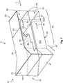
- connection arrangement according to the invention is described with respect to Fig. 1 and 2 .
- the connection arrangement shown in Fig. 1 is thereby provided with a transmission member as shown in Fig. 2 .
- the connection arrangement 1 comprises an antenna 3 and a transmission member 5.
- the arrangement 1 is shown in a transmission state T in Fig. 1 .
- the antenna arrangement 3 and the transmission member 5 are arranged such that electromagnetic waves can be coupled from the antenna 3 into the transmission member 5 and vice versa.
- the transmission member 5 has an end section 6 with a free end 7.
- the end section 6 is connected to the antenna 3.
- the transmission member 5 is preferably provided with a second free end (not shown) which is formed similar to the free end 7 and which may be connected to a similar antenna arrangement (not shown).
- the connection arrangement 1 may comprise one transmission member 5 and two antennas 3.
- the antenna 3 is preferably connected to at least one communication circuit 9 which may be a transmitter, a receiver or a combined transceiver. Further, the antenna 3 is preferably connected to a printed circuit board (PCB) 11 or monolithically integrated with the same.
- PCB printed circuit board
- the antenna 3 itself is preferably formed as PCB, in particular a low-loss PCB at millimeter-wave frequency range.
- the antenna 3 may be rigid or flexible.
- the antenna 3 has preferably an overall rectangular shape (indicated by dashed line in Fig.1 ).
- the rectangular shape preferably extends parallel to or identical with the plane 13 of the printed circuit board 11.
- the antenna 3 preferably protrudes away from the PCB 11 along a longitudinal direction L, such that it extends beyond a front edge 15 of the PCB 11, such that a connection with the transmission member 5 is possible.
- the transmission member 5 has an overall longitudinal shape and preferably extends along the longitudinal direction L in the transmission state T.
- a core 17 of the transmission member 5 is made from polymer fiber 19.
- the core 17 may be made from other materials, in particular polymer materials.
- foamed polymer material may be made from materials such as glass.
- At least the core 17 is preferably solid, except for the free ends where recesses may be present.
- the core 17 may be surrounded along a circumferential direction by additional layers which can be chosen according to the required electric and/or mechanic properties.
- the layers may surround the core 17 in a sleeve-like manner.
- the core 17 is surrounded by a dielectric layer 21, a shield 22 and an outer layer 23.
- the dielectric layer 21 is made from a material with a dielectric constant that is lower than that of the core 17.
- the shield 22 is preferably formed as metallic shield 22 for signal confinement and the outer layer 23 may be made from plastic material for protection of the transmission member 5.
- the transmission member 5 is provided with a recess 25 which is formed as slit 27.
- the recess 25 extends through a center 29 of the cross section of the transmission member 5. Thereby, the cross section runs perpendicular to the longitudinal direction L.
- the recess 25 extends from the free end 7 into the transmission member 5 along the longitudinal direction L.
- the end of the recess 25 is formed by the bottom 31.
- the transmission member 5 is laterally opened by the recess 25 in the end section 6.
- the recess 25 also extends through the layers 21, 22 and 23.
- the openings in the layers 21, 22 and 23 are arranged diametrically to each other across the center 29.
- a penetration depth 33 of the recess 25 into the transmission member 5 is, in the first embodiment, larger than an outer diameter 35 of the transmission member 5.
- the penetration depth 33 which is measured from the free end 7 to the bottom 31 along the longitudinal direction L is preferably larger than 0% and up to 200% of the diameter 35.
- the recess 25 is formed complementary to the antenna 3 such that the antenna 3 can be received in the recess 25, at least with its common layer end face 40.
- This transmission state T is shown in Fig. 1 .
- the antenna 3 abuts the bottom 31 in the transmission state T.
- the transmission member 5 may have a closed end 7 without a recess 25.
- the antenna 3 may abut the transmission member 5 with its common layer end face instead of being inserted into the transmission member 5. It should also be noted that the antenna 3 may also be used without transmission member 5 for wireless applications.
- a thickness 37 of the antenna is preferably identical to a width 39 of the slit 27.
- the thickness 37 and the width 39 are measured perpendicular to the longitudinal direction L and perpendicular to the plane 41 of the antenna 3 in the transmission state T.
- the plane 41 of the antenna 3 is preferably parallel to or identical with the plane 13 of the PCB 11.
- the antenna 3 may be tightly fitted in the recess 25 such that no or only a very small amount of a surrounding medium such as air is present between the antenna 3 and the material of the core 17 in the transmission state T.
- “being identical” includes typical deviations due to the production, which may sum up to around 5% of the thickness 37 and or the width 39.
- the thickness 37 of the antenna 3 is preferably less than 25% of the diameter 35 of the transmission member 5 in this embodiment.
- the plane 41 of the antenna 3 extends parallel to the longitudinal direction L thereby, the antenna 3 and the transmission member 5 are arranged along the same axis, which is defined by the longitudinal direction L. This improves the signal transmission between the antenna 3 and the transmission member 5 and may reduce signal loss.
- Inserting the antenna 3 into the recess 25 of the transmission member 5 facilitates coupling of these components. Thereby, a compact design is achieved and the coupling performance between the antenna 3 and the transmission member 5 may be improved.
- connection arrangement 1 Another preferred embodiment of a connection arrangement 1 is now described with respect to Figs. 3 to 5 , wherein Fig. 4 shows the embodiment of Fig. 3 in a cut-out view and Fig. 5 shows the antenna 3 with the layers made transparent for better visibility.
- Figs. 3 to 5 Details of a preferred embodiment of an antenna 3 according to the invention are described with respect to Figs. 3 to 5 .
- the antenna 3, which is shown in Figs. 3 to 5 may also be used in a connection arrangement 1, in which the antenna 3 abuts the transmission member 5 without being inserted into same, or in applications without transmission member 5.
- the recess 25, which is formed as slit 27 has a penetration depth 33 which is smaller than 50% of the diameter 35 of the transmission member 5.
- the depth 33 may preferably be larger than 0% and up to 200 % of the diameter 35.
- the width 39 of the slit 27 is, in this embodiment, larger than the penetration depth 33.
- the depth 33 is consequently 0 % of the diameter 35.
- the antenna 3 is formed as a printed circuit board 43 with two planar layers 45 and 47 and a separation layer 49, or septum.
- the separation layer 49 is preferably formed as microstrip 51.
- the separation layer 49 is preferably made from copper or metal which contains mostly copper.
- the layers 45 and 47 each extend along layer planes 46 and 48 (indicated by dashed lines in Fig. 3 ). Consequently, the separation layer 49 extends planar and parallel to the planes 46 and 48.
- the layers 45 and 47 are stacked perpendicular to the layer planes 46 and 48 and end at a common layer end face 40.
- the common layer end face 40 extends perpendicular to the layer planes 46 and 48.
- the common layer end face 40 can be used as entrance for incoming and as exit for outgoing electromagnetic waves (not shown).
- Each of the planar layers 45 and 47 provides a waveguide 50 and 52 for the transmission of electromagnetic waves parallel to the layer planes 46 and 48.
- the waveguides 50 and 52 are adapted for guiding electromagnetic waves along transmission directions 54 and 56 of the antenna 3. Consequently, the transmission directions 54 and 56 run parallel with the layer planes 46 and 48.
- the transmission directions 54 and 56 extend perpendicular to the common layer end face 40.
- Each of the waveguides 50 and 52 can be used for either incoming or outgoing electromagnetic radiation. Consequently, the antenna 3 can be used for full duplex communication.
- the longitudinal direction L of the transmission member 5 preferably extends parallel with the transmission directions 54 and 56.
- each waveguide 50 and 52 is bordered by lateral guiding elements 58.
- the layers 45 and 47 are provided with a plurality of through holes, or vias, 53 as lateral guiding elements 58.
- the through holes 53 can be used for adjusting the electromagnetic properties of the antenna 3.
- the through holes 53 basically extend perpendicular to the longitudinal direction L and to the layer planes 46 and 48.
- the through holes 53 are preferably provided with metalized inner walls 60.
- each waveguide 50 and 52 is bordered by a plurality of through holes 53 on each side perpendicular to the transmission directions 54 and 56.
- the separation layer 49 comprises a structure which is capable of polarizing electromagnetic radiation which is emitted from the antenna 3.
- the antenna 3 is therefore provided with a polarizing element 55.
- the polarizing element 55 is a circular polarizer 57.
- the polarizing element 55 is formed as an asymmetry in the shape of the separation layer 49. Thereby, the asymmetry is seen with respect to a plane P of mirror symmetry extending parallel with the transmission directions 54 and 56 and perpendicular to the layer planes 46 and 48.
- the plane P of mirror symmetry is indicated by dashed lines in Fig. 5 .
- the structure has an overall U-shape 59 which is formed as a recess 61 which extends from the common layer end face 40 into the separation layer 49 parallel to the transmission directions 54 and 56.
- the U-shape comprises a first leg 63 and a second leg 65 which extend parallel to the transmission directions 54 and 56, wherein free ends 67 and 69 of the legs 63 and 65 point in the direction of the common layer end face 40.
- the first leg 63 comprises an inner side 75 which runs basically parallel to the transmission directions 54 and 56.
- the opposite second leg 65 comprises a stepped structure 77 on its inner side 79 such that a width 81 of the second leg 65 stepwise increases from the free end 69 towards the bottom 73.
- the width 81 of the leg 65 is measured perpendicular to the transmission directions 54 and 56 and in the plane of the separation layer 49.
- Each of the steps 83 has a first edge 85 and a second edge 87, which are arranged perpendicular to each other.
- the first edge 85 basically extends parallel with the transmission directions 54 and 56 and, consequently, the second edge 87 basically extends perpendicular to the transmission directions 54 and 56.
- the lengths of the first edges 85 increases for each step 83 parallel to the transmission directions 54 and 56 from the bottom 73 towards the free end 69.
- the polarizing element 55 is at least partially inserted in the recess 25 in the transmission state T.
- the layers 45 and 47 are both covered with metallic cover layers 62 and 64.
- the cover layers 62 and 64 help to confine electromagnetic waves in the layers 45 and 47.
- the cover layers 62 and 64 are made transparent in Figs. 3 and 4 for better visibility of the remaining components of the antenna 3.
- Fig. 6 shows another preferred embodiment of an antenna 3 according to the invention.
- the antenna 3 differs from the embodiments as described before in that the lateral guiding elements 58 are formed by through holes 53 which are arranged in a single row 66 on each lateral side of the waveguides 50 and 52.
- front rows 68 of through holes 53 extend in each layer 45 and 47 on both lateral sides of the waveguides 50 and 52.
- the front rows 68 extend parallel with the common layer end face 40.
- the planar layers 45 and 47 are made transparent here for a better visibility.
- FIG. 7 another preferred embodiment of an antenna 3 for a connection arrangement 1 according to the invention is shown.
- the antenna 3 may for example be used in the arrangement 1 as described with respect to Figs. 3 and 4 .
- the antenna 3 may also be used in an embodiment of a connection arrangement 1, in which the antenna 3 abuts the transmission member 5 with the common layer end face 40 instead of being inserted into the transmission member 5. Furthermore, the antenna 3 may also be used without transmission member 5, for example in wireless applications.
- the antenna 3 has an overall longitudinal shape extending along the longitudinal direction L. In the longitudinal direction L, the antenna 3 has a connection end 89 and a front end 91. The connection end 89 can be used for connecting the antenna 3 to a communication circuit 9 (not shown here).
- the front end 91 comprises the common layer end face 40 and can be used for being coupled to a transmission member 5 (not shown here).
- the front end 91 can be used for being coupled to a transmission member 5 as described with respect to Figs. 3 and 4 either by being inserted into same or abutting a transmission member 5 which is not provided with a recess 25.
- the antenna 3 may also be used without transmission member 5 for its use in wireless application.
- the antenna 3 has a constant thickness 37 along the longitudinal direction L. However, a width 93 of the antenna 3 varies along the longitudinal direction L. The width 93 of the antenna 3 is measured perpendicular to the longitudinal direction L and perpendicular to the direction of the thickness 37.
- the width 93 of the antenna 3 varies such that a first section 95 is formed, which has a constantly shaped cross section along the longitudinal direction L. In other words, the width 93 and the thickness 37 of the antenna 3 remain constant along the longitudinal direction L in the first section 95.
- the first section 95 starts at the connection end 89 and extends in the direction of the front end 91.
- the width 93 of the antenna 3 varies along the longitudinal direction L.
- the width 93 varies such that it is larger than in the first section 95 at the front end 91 and decreases towards the first section 95.
- the antenna 3 and its waveguides 50 and 52 broaden towards the common layer end face 40 in the second section 97. Seen along the direction of the thickness 37 of the antenna 3, the antenna 3 thereby has an overall funnel-like shape.
- the antenna 3 in this embodiment comprises two planar layers 45 and 47 and a separation layer 49, which is arranged between the planar layers 45 and 47.
- the planar layers 45 and 47 are preferably made from a dielectric material, for example the material of a printed circuit board.
- the separation layer 49 comprises a polarizing element 55, in particular a circular polarizer 57 which is formed as a microstrip 51.
- the circular polarizer 57 comprises steps 83 which form a step structure 77.
- a width 99 of the circular polarizer 57 decreases with every step 83 in the longitudinal direction L towards the second section 97.
- the polarizer 57 is basically shaped as the second leg 65 as described with respect to Fig. 4 .
- the polarizing element 55 is also here formed by an asymmetry in the shape of the separation layer 49.
- the plane of mirror symmetry extends along the longitudinal direction L and perpendicular to the layer planes 46 and 48 or, in other words to the plane 41 of the antenna 3.
- a dashed line indicates where the plane P cuts the separation layer 49.
- the planar layers 45 and 47 are not provided with vias or through holes 53 as the embodiments described above. Instead, the antenna 3 comprises metalized sidewalls 103.
- the sidewalls 103 are arranged opposite to each other along the direction of the width 93 of the antenna 3. Consequently, the sidewalls 103 extend parallel with each other in the first section 95 and diverge in the second section 97.
- the planar layers 45 and 47 are covered with metallic cover layers 62 and 64 on top and bottom of the antenna 3.
- the metallic cover layers 62 and 64 are arranged parallel with each other and extend parallel with the direction of the width 93 of the antenna 3 and the longitudinal direction L.
Abstract

Description
- The invention relates to an antenna for transmitting and/or receiving electromagnetic waves, in particular in the millimeter-wave frequency range, especially for communication purposes. The invention further relates to connection arrangements for the transmission and reception of electromagnetic waves, in particular in the millimeter-wave frequency range.
- Antennas and connection arrangements as mentioned above are known in the prior art. Generally, antennas for transmitting and/or receiving electromagnetic waves, in particular in the millimeter-wave frequency range, require a large area and/or construction space. This makes the integration of components into system with a small amount of available space difficult.
- It is therefore an object of the invention to overcome this problem and to provide an antenna and connection arrangements which allow to save space.
- This object is achieved for the above-mentioned antenna in that the antenna comprises two basically planar layers which are stacked perpendicular to the layer planes and which are at least partially separated by at least one separation layer, wherein the planar layers each end at a common layer end face, and wherein the planar layers each provide a waveguide for the transmission of electromagnetic waves parallel to the layer planes, the waveguides ending at the common layer end face.
- For one of the above-mentioned connection arrangements, the object is achieved in that the arrangement comprises at least one antenna according to the invention and at least one transmission member for transporting said waves, wherein, at least in a transmission state, the at least one transmission member abuts the common layer end face.
- For another of the above-mentioned connection arrangements, the object is achieved in that the arrangement comprises at least one antenna according to the invention and at least one transmission member for transporting said waves, wherein the at least one transmission member is provided with at least one recess which extends from a free end of the at least one transmission member into the same, and in that, at least in a transmission state, the at least one common layer end face is at least partially inserted in the at least one recess.
- The solution according to the invention allows the production of compact devices. The common layer end face may serve as entrance for incoming and as exit for outgoing electromagnetic waves. Since the common layer end face is formed by the narrow sides of the layers, the common layer end face has, at least in the direction perpendicular to the layers planes, a size which is in the range of the sum of the layer thicknesses.
- The waveguides in the layers define transmission directions for the electromagnetic waves. These directions are generally parallel to the layer planes. The common layer end face extends preferably perpendicular to these transmission directions and, consequently, to the layer planes.
- In the following, further improvements of the invention are described. The additional improvements may be combined independently of each other, depending on whether a particular advantage of a particular improvement is needed in a specific application.
- According to a first advantageous improvement, one of the waveguides can be used for incoming electromagnetic waves and the other waveguide may be used for outgoing electromagnetic waves. This allows to use the same antenna for incoming and outgoing electromagnetic waves, in particular at the same time.
- The two planar layers are preferably made from similar material, in particular from dielectric material. For example, the layers can be made from typical material for printed circuit boards (PCB) such as, but not limited to, liquid crystal polymers (LCP), Teflon or FR-4 epoxy resin systems.
- The at least one separation layer may be made from a metallic material. Thereby, a good separation and electric insulation between the two waveguides can be achieved.
- The separation layer may in particular be a microstrip. Consequently, the antenna may be formed as PCB with two dielectric layers and a microstrip between said layers.
- In order to improve the wave guiding properties of the planar layers, said layers can be at least partially covered with metallic cover layers. In the alternative, the cover layers can be made from a material having a dielectric constant which is different from that of the planar layers.
- For defining the transmission directions and for laterally confining electromagnetic waves in the waveguides, each waveguide may be bordered by lateral wave guiding elements. Said lateral wave guiding elements are preferably arranged parallel to the transmission direction or extend parallel to same.
- According to an advantageous embodiment, at least one lateral wave guiding element may be made from a material having a dielectric constant which is different from that of the planar layers. Additionally or alternatively, at least one lateral wave guiding element may be made from a metallic material.
- At least one lateral wave guiding element may be made as a through hole, typically called via, in at least one of the planar layers, the at least one through hole extending perpendicular to the layer planes. Such lateral wave guiding is easy to manufacture. In this case, the through hole may be filled with air as dielectric material.
- In the alternative, at least one through hole may be provided with metalized inner walls. These walls consequently form metal tubes in the layer which can act as lateral wave guiding elements.
- According to another advantageous embodiment of the lateral wave guiding element, at least one lateral wave guiding element may be formed as a side wall extending perpendicular to the layer planes and along the corresponding waveguide. The side wall may either be made from a metallic material or from a material having a dielectric constant which is different from that of the planar layers
- The waveguides may have a constant cross section along the transmission direction, wherein the cross section is defined perpendicular to the transmission direction.
- In the alternative, at least one of the waveguides may broaden towards the common layer end face, at least in a direction parallel to the plane of the layers. Consequently the cross section increases along the transmission direction towards the common layer end face. By varying the cross section, the directional radiation characteristic for outgoing waves can be tuned. If the waveguides broadens towards the common layer end face, the outgoing waves may be emitted within a smaller angle. Further, the antenna gain may be increased.
- According to another advantageous improvement of the antenna, the antenna may further provide at least one, in particular circularly, polarizing element, which is adapted to differently polarize electromagnetic waves in both waveguides. Accordingly, electromagnetic waves which are emitted from the first waveguide will have a polarization that is contrary to that of electromagnetic waves which are emitted from the second waveguide. Thereby, for outgoing waves, the waveguide can be chosen in accordance with the required polarization.
- In the preferred case of circular polarization, electromagnetic waves which are emitted from the first waveguide may have a right hand circular polarization, whereas electromagnetic waves which are emitted from the second waveguide may have a left hand circular polarization, or vice versa.
- Circular polarization has several advantages. Firstly, it allows rotational freedom of the antenna with respect to a rotation around the transmission direction. Secondly, it allows full duplex communication. One waveguide can be used for outgoing electromagnetic waves, which have, just by way of example, right hand circular polarization. If electromagnetic waves are received, which have left hand circular polarization, then these waves will be guided into the second waveguide upon entering the antenna through the common layer end face. Consequently, both waveguides can be used at the same time which enables the full duplex communication.
- For a compact and highly integrated structure, the at least one polarizing element may be formed monolithically with the at least one, in particular metallic, separation layer.
- The at least one polarizing element may easily be formed as an asymmetry in the shape of the at least one, in particular metallic, separation layer. Thereby, the asymmetry is seen with respect to a plane of mirror symmetry extending parallel with the transmission direction and perpendicular to the layer planes.
- The at least one polarizing element may preferably be formed by at least one recess which extends from the common layer end face along transmission direction into the, in particular metallic, separation layer.
- Preferably, the asymmetric shape is formed by a stepped structure in the at least one, in particular metallic, separation layer. For easily forming a circular polarizer, the separation layer may have an overall U-shape, wherein two legs of the U-shape extend towards the common layer end face. At least one of the legs may be provided with a stepped structure on its inside extending from the free end of the leg towards the bottom of the U-shape. The step-like structure may be formed such that the distance between the two legs of the U-shape increases with each step towards the free ends of the legs.
- In the case that the antenna comprises side walls as lateral wave guiding elements, the circular polarizer may also be formed as described, but without the leg of the U-shape without the stepped structure.
- According to a first advantageous improvement of a connection arrangement according to the invention, the transmission member may be a polymer fiber waveguide.
- According to a first advantageous improvement of a connection arrangement with a transmission member having a recess, the at least one recess and the at least one antenna may at least partially be formed complementary to each other. This may facilitate assembling of these, ensure a defined relative position between these and may also lead to securely fixating these components with respect to each other and therefore reduce loss.
- The at least one transmission member may have an overall longitudinal shape, at least in parts and the at least one recess may extend along a longitudinal direction of the at least one transmission member. The at least one transmission member may have in particular a circular shape in a cross section perpendicular to the longitudinal direction. Alternatively, the at least one transmission member may have any other suitable cross section, for example rectangular or polygonal. If the at least one recess extends along the longitudinal direction, then the at least one antenna may extend into the transmission member along said direction. This may facilitate coupling because electromagnetic waves which can be radiated from the at least one antenna in the longitudinal direction may easily follow the shape of the at least one transmission member.
- The at least one transmission member may, in the alternative, be short compared to the above mentioned longitudinal embodiment. In this case, the at least one transmission member may form a cap for the antenna which can be connected to other waveguiding components. Thereby, the at least one transmission member may act as interface between the at least one antenna and at least one other waveguiding component.
- The at least one antenna may have a flat shape, at least in parts. Especially for this case, the at least one recess may be formed as a slit extending into the at least one transmission member. In particular, said slit may extend parallel with the longitudinal direction of the transmission member. A flat antenna may easily be inserted into the slit. Preferably, the slit has a width which is identical to a thickness of the antenna with typical production tolerances. This may enable a secure seat of the at least one antenna in the at least one slit.
- For a good coupling quality, the at least one slit may extend through a centre of a cross section of the at least one transmission member. Thereby, the at least one antenna may be inserted in a centre region of the transmission member.
- Especially in the case that the at least one antenna has a length that extends beyond an overall thickness of the transmission member, the at least one transmission member may be laterally opened by the at least one slit. The length of the antenna is thereby measured perpendicular to the longitudinal direction of the transmission member in the transmission state. Consequently, a length of the slit is thereby identical to a thickness of the transmission member. In the case that the slit extends through a centre of a cross section of the at least one transmission member, the lateral openings in the transmission member are arranged diametrically to each other.
- The at least one recess may have a penetration depth measured from the free end of the at least one transmission member to a bottom portion of the recess, which is preferably larger than 0% and up to 200%, in particular between 25 % and 200%, of a diameter of the at least one transmission member. The penetration depth is preferably measured parallel to the longitudinal direction of the at least one transmission member.
- The at least one transmission member is preferably made from a solid material, in particular a core may be made from a solid material. The at least one transmission member may thereby be made from a polymer material. A polymer transmission member allows the setup of cost efficient connection arrangements. Further, at least one recess can easily be formed in a transmission member made from polymer material, for example by molding, cutting or other suitable techniques. The transmission member may have at least one metal shielding which circumferentially surrounds the core.
- As mentioned above, the at least one antenna may at least partially be formed as a printed circuit board. For assembling of the connection arrangement, at least parts of the printed circuit board may be inserted into the at least one recess of the transmission member. Especially in the case that the at least one antenna is at least partially formed as a printed circuit board, the at least one recess may be formed as a slit. In this case, a plane defined by the slit, which extends along a longitudinal direction of the transmission member and a length direction of the slit extends preferably parallel to a plane which is defined by the printed circuit board. Said plane is consequently perpendicular to the direction of the width of the slit.
- In order to further improve the coupling and the assembly of the connection arrangement, the at least one antenna may be provided with at least one, in particular circular, polarizer as mentioned above, wherein the at least one polarizer is at least partially arranged in the at least one recess in the transmission state. Thereby, electromagnetic radiation which was polarized by the polarizer may directly enter the at least one transmission member and vice versa. If, as preferred, the at least one polarizer is a circular polarizer and is adapted for polarizing electromagnetic radiation circularly with respect to a longitudinal direction of the transmission member, then the transmission member and the antenna can be assembled to form a connection arrangement according to the invention independently from a rotational position with respect to the longitudinal direction. If, for example, the at least one recess is formed as a slit which extends through a centre of the cross section of the transmission member, then the transmission member and the antenna can be rotated by 180 degrees around the longitudinal direction and will achieve the same coupling results in the transmission state. This leads to easier assembly of the arrangement.
- In the following, the invention and its improvements are described in greater details using exemplary embodiments and with reference to the drawings. As described above, the various features shown in the embodiments may be used independently of each other in specific applications.
- In the following figures, elements having the same function and/or the same structure will be referenced by the same reference signs.
- In the drawings:
- Fig. 1
- Shows a schematic perspective view of a preferred embodiment of a connection arrangement according to the invention in a transmission state;
- Fig. 2
- shows a schematic perspective view of the transmission member according to the invention without antenna;
- Fig. 3
- shows a schematic perspective view of a second preferred embodiment of a connection arrangement according to the invention in a transmission state;
- Fig. 4
- shows a cut-away view of the embodiment of
Fig. 3 showing a separation layer of the antenna; - Fig. 5
- shows a different view of the antenna of
Fig. 3 and 4 with the planar layers made transparent; - Fig. 6
- shows another preferred embodiment of an antenna according to the invention in a schematic perspective view
- Fig. 7
- shows another embodiment of an antenna according to the invention in a schematic perspective view.
- In the following, a first preferred embodiment of a connection arrangement according to the invention is described with respect to
Fig. 1 and 2 . The connection arrangement shown inFig. 1 is thereby provided with a transmission member as shown inFig. 2 . - The
connection arrangement 1 comprises anantenna 3 and atransmission member 5. Thearrangement 1 is shown in a transmission state T inFig. 1 . In the transmission state T, theantenna arrangement 3 and thetransmission member 5 are arranged such that electromagnetic waves can be coupled from theantenna 3 into thetransmission member 5 and vice versa. - The
transmission member 5 has anend section 6 with afree end 7. Theend section 6 is connected to theantenna 3. It should be noted that thetransmission member 5 is preferably provided with a second free end (not shown) which is formed similar to thefree end 7 and which may be connected to a similar antenna arrangement (not shown). In this case, theconnection arrangement 1 may comprise onetransmission member 5 and twoantennas 3. - The
antenna 3 is preferably connected to at least one communication circuit 9 which may be a transmitter, a receiver or a combined transceiver. Further, theantenna 3 is preferably connected to a printed circuit board (PCB) 11 or monolithically integrated with the same. Theantenna 3 itself is preferably formed as PCB, in particular a low-loss PCB at millimeter-wave frequency range. Theantenna 3 may be rigid or flexible. - The
antenna 3 has preferably an overall rectangular shape (indicated by dashed line inFig.1 ). The rectangular shape preferably extends parallel to or identical with theplane 13 of the printedcircuit board 11. Theantenna 3 preferably protrudes away from thePCB 11 along a longitudinal direction L, such that it extends beyond afront edge 15 of thePCB 11, such that a connection with thetransmission member 5 is possible. - The
transmission member 5 has an overall longitudinal shape and preferably extends along the longitudinal direction L in the transmission state T. Preferably, at least a core 17 of thetransmission member 5 is made from polymer fiber 19. Alternatively, the core 17 may be made from other materials, in particular polymer materials. For example, foamed polymer material. According to another alternative, the core 17 may be made from materials such as glass. At least the core 17 is preferably solid, except for the free ends where recesses may be present. - The core 17 may be surrounded along a circumferential direction by additional layers which can be chosen according to the required electric and/or mechanic properties. In particular, the layers may surround the core 17 in a sleeve-like manner. According to a preferred exemplary embodiment, the core 17 is surrounded by a dielectric layer 21, a
shield 22 and anouter layer 23. - Just by way of example, the dielectric layer 21 is made from a material with a dielectric constant that is lower than that of the core 17. The
shield 22 is preferably formed asmetallic shield 22 for signal confinement and theouter layer 23 may be made from plastic material for protection of thetransmission member 5. - In the
end section 6, thetransmission member 5 is provided with a recess 25 which is formed as slit 27. The recess 25 extends through acenter 29 of the cross section of thetransmission member 5. Thereby, the cross section runs perpendicular to the longitudinal direction L. The recess 25 extends from thefree end 7 into thetransmission member 5 along the longitudinal direction L. The end of the recess 25 is formed by the bottom 31. - The
transmission member 5 is laterally opened by the recess 25 in theend section 6. In other words, the recess 25 also extends through thelayers layers center 29. Apenetration depth 33 of the recess 25 into thetransmission member 5 is, in the first embodiment, larger than anouter diameter 35 of thetransmission member 5. - However, this is not mandatory. Preferably, the
penetration depth 33, which is measured from thefree end 7 to the bottom 31 along the longitudinal direction L is preferably larger than 0% and up to 200% of thediameter 35. - Preferably, the recess 25 is formed complementary to the
antenna 3 such that theantenna 3 can be received in the recess 25, at least with its commonlayer end face 40. This transmission state T is shown inFig. 1 . Preferably, theantenna 3 abuts the bottom 31 in the transmission state T. - It should be noted that, according to another embodiment of a
connection arrangement 1 according to the invention, thetransmission member 5 may have aclosed end 7 without a recess 25. In this case, theantenna 3 may abut thetransmission member 5 with its common layer end face instead of being inserted into thetransmission member 5. It should also be noted that theantenna 3 may also be used withouttransmission member 5 for wireless applications. - A
thickness 37 of the antenna is preferably identical to awidth 39 of the slit 27. Preferably, thethickness 37 and thewidth 39 are measured perpendicular to the longitudinal direction L and perpendicular to theplane 41 of theantenna 3 in the transmission state T. Theplane 41 of theantenna 3 is preferably parallel to or identical with theplane 13 of thePCB 11. In the case that thethickness 37 and thewidth 39 are identical, theantenna 3 may be tightly fitted in the recess 25 such that no or only a very small amount of a surrounding medium such as air is present between theantenna 3 and the material of the core 17 in the transmission state T. It should be noted that "being identical" includes typical deviations due to the production, which may sum up to around 5% of thethickness 37 and or thewidth 39. Thethickness 37 of theantenna 3 is preferably less than 25% of thediameter 35 of thetransmission member 5 in this embodiment. - In the transmission state T, the
plane 41 of theantenna 3 extends parallel to the longitudinal direction L thereby, theantenna 3 and thetransmission member 5 are arranged along the same axis, which is defined by the longitudinal direction L. This improves the signal transmission between theantenna 3 and thetransmission member 5 and may reduce signal loss. - Inserting the
antenna 3 into the recess 25 of thetransmission member 5 facilitates coupling of these components. Thereby, a compact design is achieved and the coupling performance between theantenna 3 and thetransmission member 5 may be improved. - Another preferred embodiment of a
connection arrangement 1 is now described with respect toFigs. 3 to 5 , whereinFig. 4 shows the embodiment ofFig. 3 in a cut-out view andFig. 5 shows theantenna 3 with the layers made transparent for better visibility. - Further, details of a preferred embodiment of an
antenna 3 according to the invention are described with respect toFigs. 3 to 5 . Theantenna 3, which is shown inFigs. 3 to 5 may also be used in aconnection arrangement 1, in which theantenna 3 abuts thetransmission member 5 without being inserted into same, or in applications withouttransmission member 5. - For the sake of brevity, only the differences to the aforementioned embodiments are described in detail.
- The recess 25, which is formed as slit 27 has a
penetration depth 33 which is smaller than 50% of thediameter 35 of thetransmission member 5. Alternatively, thedepth 33 may preferably be larger than 0% and up to 200 % of thediameter 35. Thewidth 39 of the slit 27 is, in this embodiment, larger than thepenetration depth 33. - In the case of a
different connection arrangement 1, in which theantenna 3 abuts thetransmission member 5 without being inserted, thedepth 33 is consequently 0 % of thediameter 35. - The
antenna 3 is formed as a printed circuit board 43 with twoplanar layers layers Fig. 3 ). Consequently, the separation layer 49 extends planar and parallel to theplanes - The
layers layer end face 40. Preferably, the commonlayer end face 40 extends perpendicular to the layer planes 46 and 48. - The common
layer end face 40 can be used as entrance for incoming and as exit for outgoing electromagnetic waves (not shown). - Each of the
planar layers waveguide waveguides transmission directions antenna 3. Consequently, thetransmission directions transmission directions layer end face 40. - Each of the
waveguides antenna 3 can be used for full duplex communication. In an embodiment, in which theantenna 3 is coupled to atransmission member 5, either by abutting saidtransmission member 5 or by being inserted into a recess 25 of thetransmission member 5, the longitudinal direction L of thetransmission member 5 preferably extends parallel with thetransmission directions - For guiding electromagnetic waves laterally, wherein laterally means perpendicular to the
transmission directions waveguide - The
layers antenna 3. The through holes 53 basically extend perpendicular to the longitudinal direction L and to the layer planes 46 and 48. The through holes 53 are preferably provided with metalizedinner walls 60. - In the embodiment of the
antenna 3 as shown inFigs. 3 to 5 , eachwaveguide transmission directions - The separation layer 49 comprises a structure which is capable of polarizing electromagnetic radiation which is emitted from the
antenna 3. Theantenna 3 is therefore provided with a polarizing element 55. Preferably, the polarizing element 55 is a circular polarizer 57. - The polarizing element 55 is formed as an asymmetry in the shape of the separation layer 49. Thereby, the asymmetry is seen with respect to a plane P of mirror symmetry extending parallel with the
transmission directions Fig. 5 . - The structure has an overall U-shape 59 which is formed as a recess 61 which extends from the common
layer end face 40 into the separation layer 49 parallel to thetransmission directions first leg 63 and asecond leg 65 which extend parallel to thetransmission directions legs layer end face 40. - The free space 71 between the
legs transmission directions first leg 63 comprises aninner side 75 which runs basically parallel to thetransmission directions - The opposite
second leg 65 comprises a steppedstructure 77 on itsinner side 79 such that awidth 81 of thesecond leg 65 stepwise increases from thefree end 69 towards the bottom 73. Thewidth 81 of theleg 65 is measured perpendicular to thetransmission directions - Each of the
steps 83 has afirst edge 85 and asecond edge 87, which are arranged perpendicular to each other. Thefirst edge 85 basically extends parallel with thetransmission directions second edge 87 basically extends perpendicular to thetransmission directions first edges 85 increases for eachstep 83 parallel to thetransmission directions free end 69. - In the embodiment, in which the
antenna 3 is inserted into the recess 25 of thetransmission member 5, the polarizing element 55 is at least partially inserted in the recess 25 in the transmission state T. - In order to improve the wave guiding properties of the
waveguides layers layers Figs. 3 and 4 for better visibility of the remaining components of theantenna 3. -
Fig. 6 shows another preferred embodiment of anantenna 3 according to the invention. - Also here, for the sake of brevity, only the differences to the aforementioned embodiments are described.
- The
antenna 3 differs from the embodiments as described before in that the lateral guiding elements 58 are formed by through holes 53 which are arranged in asingle row 66 on each lateral side of thewaveguides layer end face 40,front rows 68 of through holes 53 extend in eachlayer waveguides front rows 68 extend parallel with the commonlayer end face 40. Theplanar layers - In
Fig. 7 , another preferred embodiment of anantenna 3 for aconnection arrangement 1 according to the invention is shown. Theantenna 3 may for example be used in thearrangement 1 as described with respect toFigs. 3 and 4 . - Of course, the
antenna 3 may also be used in an embodiment of aconnection arrangement 1, in which theantenna 3 abuts thetransmission member 5 with the commonlayer end face 40 instead of being inserted into thetransmission member 5. Furthermore, theantenna 3 may also be used withouttransmission member 5, for example in wireless applications. - For the sake of brevity, only the differences to the aforementioned embodiments are described in detail.
- The
antenna 3 has an overall longitudinal shape extending along the longitudinal direction L. In the longitudinal direction L, theantenna 3 has aconnection end 89 and afront end 91. Theconnection end 89 can be used for connecting theantenna 3 to a communication circuit 9 (not shown here). - The
front end 91 comprises the commonlayer end face 40 and can be used for being coupled to a transmission member 5 (not shown here). In particular, thefront end 91 can be used for being coupled to atransmission member 5 as described with respect toFigs. 3 and 4 either by being inserted into same or abutting atransmission member 5 which is not provided with a recess 25. - Of course, the
antenna 3 may also be used withouttransmission member 5 for its use in wireless application. - The
antenna 3 has aconstant thickness 37 along the longitudinal direction L. However, awidth 93 of theantenna 3 varies along the longitudinal direction L. Thewidth 93 of theantenna 3 is measured perpendicular to the longitudinal direction L and perpendicular to the direction of thethickness 37. - The
width 93 of theantenna 3 varies such that afirst section 95 is formed, which has a constantly shaped cross section along the longitudinal direction L. In other words, thewidth 93 and thethickness 37 of theantenna 3 remain constant along the longitudinal direction L in thefirst section 95. Thefirst section 95 starts at theconnection end 89 and extends in the direction of thefront end 91. - In a
second section 97 of theantenna 3, thewidth 93 of theantenna 3 varies along the longitudinal direction L. Thereby, thewidth 93 varies such that it is larger than in thefirst section 95 at thefront end 91 and decreases towards thefirst section 95. In other words, theantenna 3 and itswaveguides layer end face 40 in thesecond section 97. Seen along the direction of thethickness 37 of theantenna 3, theantenna 3 thereby has an overall funnel-like shape. - As the embodiments described with respect to
Figs. 3 to 6 , theantenna 3 in this embodiment comprises twoplanar layers planar layers planar layers - The separation layer 49 comprises a polarizing element 55, in particular a circular polarizer 57 which is formed as a microstrip 51. The circular polarizer 57 comprises
steps 83 which form astep structure 77. Awidth 99 of the circular polarizer 57 decreases with everystep 83 in the longitudinal direction L towards thesecond section 97. In other words, the polarizer 57 is basically shaped as thesecond leg 65 as described with respect toFig. 4 . - Consequently, the polarizing element 55 is also here formed by an asymmetry in the shape of the separation layer 49. Hereby, the plane of mirror symmetry extends along the longitudinal direction L and perpendicular to the layer planes 46 and 48 or, in other words to the
plane 41 of theantenna 3. InFig. 7 a dashed line indicates where the plane P cuts the separation layer 49. - The
planar layers antenna 3 comprises metalizedsidewalls 103. Thesidewalls 103 are arranged opposite to each other along the direction of thewidth 93 of theantenna 3. Consequently, thesidewalls 103 extend parallel with each other in thefirst section 95 and diverge in thesecond section 97. - The
planar layers antenna 3. The metallic cover layers 62 and 64 are arranged parallel with each other and extend parallel with the direction of thewidth 93 of theantenna 3 and the longitudinal direction L. -
- 1
- connection arrangement
- 3
- antenna
- 5
- transmission member
- 6
- end section
- 7
- free end of transmission member
- 9
- communication circuit
- 11
- printed circuit board (PCB)
- 13
- plane of printed circuit board
- 15
- front edge of printed circuit board
- 17
- core
- 19
- polymer material
- 21
- dielectric layer
- 22
- shield
- 23
- outer layer
- 25
- recess
- 27
- slit
- 29
- center
- 31
- bottom
- 33
- penetration depth
- 35
- diameter of the transmission member
- 37
- thickness of antenna
- 39
- width
- 40
- common layer end face
- 41
- plane of the antenna
- 43
- printed circuit board
- 45
- planar layer
- 46
- layer plane
- 47
- planar layer
- 48
- layer plane
- 49
- separation layer
- 50
- waveguide
- 51
- microstrip
- 52
- waveguide
- 53
- through holes
- 54
- transmission direction
- 55
- polarizing element
- 56
- transmission direction
- 57
- circular polarizer
- 58
- lateral wave guiding element
- 59
- U-shape
- 60
- metalized inner walls
- 61
- recess
- 62
- metallic cover layer
- 63
- first leg
- 64
- metallic cover layer
- 65
- second leg
- 66
- row
- 67
- free end of first leg
- 68
- front row
- 69
- free end of second leg
- 71
- free space between legs
- 73
- bottom of the U-shape
- 75
- inner side of the first leg
- 77
- stepped structure
- 79
- inner side of the second leg
- 81
- width of the second leg
- 83
- step
- 85
- first edge of the step
- 87
- second edge of the step
- 89
- connection end
- 91
- front end
- 93
- width of the antenna
- 95
- first section
- 97
- second section
- 99
- width of the polarizing element
- 103
- sidewall
- L
- longitudinal direction
- P
- plane of mirror symmetry
- T
- transmission state
Claims (15)
- Antenna (3) for transmitting and/or receiving electromagnetic waves, in particular in the millimeter-range, the antenna (3) comprising two basically planar layers (45, 47) which are stacked perpendicular to the layer planes (46, 48) and which are at least partially separated by at least one separation layer (49), wherein the planar layers (45, 47) each end at a common layer end face (40), and wherein the planar layers (45, 47) each provide a waveguide (50, 52) for the transmission of electromagnetic waves parallel to the layer planes (46, 48), the waveguides (50, 52) ending at the common layer end face (40).
- Antenna (3) according to claim 1, wherein the at least one separation layer (49) is made from a metallic material.
- Antenna (3) according to claim 1 or 2, wherein the two planar layers (45, 47) are at least partially covered with metallic cover layers (62, 64).
- Antenna (3) according to any of claims 1 to 3, wherein each waveguide (50, 52) is bordered by lateral wave guiding elements (58).
- Antenna (3) according to claim 4, wherein at least one lateral wave guiding element (58) is made from a material having a dielectric constant which is different from that of the planar layers (45, 47).
- Antenna (3) according to claim 4 or 5, wherein at least one lateral wave guiding element (58) is made from a metallic material.
- Antenna (3) according to any of claims 4 to 6, wherein at least one lateral wave guiding element (58) is made as a through hole (53) in a planar layer (45, 47), extending perpendicular to the layer planes (46, 48).
- Antenna (3) according to any of claims 4 to 7, wherein at least one lateral wave guiding element (58) is formed as a side wall (103) extending perpendicular to the layer planes (46, 48) and along the corresponding waveguide (50, 52).
- Antenna (3) according to any of claims 1 to 8, wherein at least one of the waveguides (50, 52) broadens towards the common layer end face (40), at least in a direction parallel to the plane of the layers (46, 48).
- Antenna (3) according to any of claims 1 to 9, wherein the antenna (3) further provides at least one polarizing element (55) which is adapted to differently polarize electromagnetic waves in the waveguides (50, 52).
- Antenna (3) according to claim 10, wherein the at least one polarizing element (55) is formed monolithically with the at least one separation layer (49).
- Antenna (3) according to claim 11, wherein the at least one polarizing element (55) is formed as an asymmetry in the shape of the at least one separation layer (49).
- Antenna (3) according claim 12, wherein the asymmetric shape is formed by a stepped structure (77) in the at least one separation layer (49).
- Connection arrangement (1) for the transmission and reception of electromagnetic waves, in particular in the millimeter-range, the arrangement comprising at least one antenna (3) according to any of claims 1 to 13 and at least one transmission member (5) for transporting said waves, wherein, at least in a transmission state (T), the at least one transmission member (5) abuts the common layer end face (40).
- Connection arrangement (1) for the transmission and reception of electromagnetic waves, in particular in the millimeter-range, the arrangement comprising at least one antenna (3) according to any of claims 1 to 13 and at least one transmission member (5) for transporting said waves, wherein the at least one transmission member (5) is provided with at least one recess (25) which extends from a free end (7) of the at least one transmission member (5) into the same, and in that, at least in a transmission state (T), the at least one common layer end face (40) is at least partially inserted in the at least one recess (25).
Priority Applications (6)
| Application Number | Priority Date | Filing Date | Title |
|---|---|---|---|
| EP16206808.4A EP3340370A1 (en) | 2016-12-23 | 2016-12-23 | Millimeter wave antenna and connection arrangements |
| PCT/EP2017/083803 WO2018115115A1 (en) | 2016-12-23 | 2017-12-20 | Millimeter wave antenna and connection arrangements |
| CN201780079034.6A CN110088975A (en) | 2016-12-23 | 2017-12-20 | Millimeter wave antenna and attachment device |
| JP2019533368A JP2020502937A (en) | 2016-12-23 | 2017-12-20 | Millimeter wave antenna and connection device |
| EP17836023.6A EP3560027A1 (en) | 2016-12-23 | 2017-12-20 | Millimeter wave antenna and connection arrangements |
| US16/447,451 US20190305409A1 (en) | 2016-12-23 | 2019-06-20 | Millimeter Wave Antenna and Connection Arrangements |
Applications Claiming Priority (1)
| Application Number | Priority Date | Filing Date | Title |
|---|---|---|---|
| EP16206808.4A EP3340370A1 (en) | 2016-12-23 | 2016-12-23 | Millimeter wave antenna and connection arrangements |
Publications (1)
| Publication Number | Publication Date |
|---|---|
| EP3340370A1 true EP3340370A1 (en) | 2018-06-27 |
Family
ID=57609795
Family Applications (2)
| Application Number | Title | Priority Date | Filing Date |
|---|---|---|---|
| EP16206808.4A Ceased EP3340370A1 (en) | 2016-12-23 | 2016-12-23 | Millimeter wave antenna and connection arrangements |
| EP17836023.6A Withdrawn EP3560027A1 (en) | 2016-12-23 | 2017-12-20 | Millimeter wave antenna and connection arrangements |
Family Applications After (1)
| Application Number | Title | Priority Date | Filing Date |
|---|---|---|---|
| EP17836023.6A Withdrawn EP3560027A1 (en) | 2016-12-23 | 2017-12-20 | Millimeter wave antenna and connection arrangements |
Country Status (5)
| Country | Link |
|---|---|
| US (1) | US20190305409A1 (en) |
| EP (2) | EP3340370A1 (en) |
| JP (1) | JP2020502937A (en) |
| CN (1) | CN110088975A (en) |
| WO (1) | WO2018115115A1 (en) |
Cited By (1)
| Publication number | Priority date | Publication date | Assignee | Title |
|---|---|---|---|---|
| EP4125152A1 (en) * | 2021-07-30 | 2023-02-01 | Aptiv Technologies Limited | Dual-mode interconnect assembly between radio-frequency integrated circuits and a plastic waveguide |
Families Citing this family (2)
| Publication number | Priority date | Publication date | Assignee | Title |
|---|---|---|---|---|
| CN107646091B (en) * | 2015-04-14 | 2019-11-15 | 模拟技术公司 | Detector array for radiating system |
| FR3135355B1 (en) * | 2022-05-04 | 2024-03-22 | Psa Automobiles Sa | Assembly for connecting at least one track of a printed circuit to a plastic waveguide |
Citations (2)
| Publication number | Priority date | Publication date | Assignee | Title |
|---|---|---|---|---|
| US20150185425A1 (en) * | 2012-07-10 | 2015-07-02 | 3M Innovative Properties Company | Wireless connector with a hollow telescopic waveguide |
| EP2940784A1 (en) * | 2012-12-27 | 2015-11-04 | Fujikura Ltd. | Mode converter |
Family Cites Families (5)
| Publication number | Priority date | Publication date | Assignee | Title |
|---|---|---|---|---|
| JPS61150501A (en) * | 1984-12-25 | 1986-07-09 | Nec Corp | Mode converter |
| JPH11308025A (en) * | 1998-04-22 | 1999-11-05 | Kyocera Corp | Directional coupler |
| JP2001230608A (en) * | 2000-02-18 | 2001-08-24 | Matsushita Electric Ind Co Ltd | Dielectric line |
| JP2007329741A (en) * | 2006-06-08 | 2007-12-20 | Sharp Corp | Circle-linear polarization converter, satellite signal receiving converter, and antenna unit |
| JP6104672B2 (en) * | 2013-03-29 | 2017-03-29 | モレックス エルエルシー | High frequency transmission equipment |
-
2016
- 2016-12-23 EP EP16206808.4A patent/EP3340370A1/en not_active Ceased
-
2017
- 2017-12-20 JP JP2019533368A patent/JP2020502937A/en active Pending
- 2017-12-20 CN CN201780079034.6A patent/CN110088975A/en active Pending
- 2017-12-20 WO PCT/EP2017/083803 patent/WO2018115115A1/en unknown
- 2017-12-20 EP EP17836023.6A patent/EP3560027A1/en not_active Withdrawn
-
2019
- 2019-06-20 US US16/447,451 patent/US20190305409A1/en not_active Abandoned
Patent Citations (2)
| Publication number | Priority date | Publication date | Assignee | Title |
|---|---|---|---|---|
| US20150185425A1 (en) * | 2012-07-10 | 2015-07-02 | 3M Innovative Properties Company | Wireless connector with a hollow telescopic waveguide |
| EP2940784A1 (en) * | 2012-12-27 | 2015-11-04 | Fujikura Ltd. | Mode converter |
Non-Patent Citations (2)
| Title |
|---|
| DOW-CHIH NIU ET AL: "Application of FDTD for analysis of waveguide transition", DIGEST OF THE ANTENNAS AND PROPAGATION SOCIETY INTERNATIONAL SYMPOSIUM. SEATTLE, WA., JUNE 19 - 24, 1994; [DIGEST OF THE ANTENNAS AND PROPAGATION SOCIETY INTERNATIONAL SYMPOSIUM], NEW YORK, IEEE, US, 20 June 1994 (1994-06-20), pages 1782, XP032367822, ISBN: 978-0-7803-2009-3, DOI: 10.1109/APS.1994.408193 * |
| KARSTEN KUHLMANN ET AL: "Circularly Polarized Substrate-Integrated Waveguide Antenna Array at Ka-Band", PROC. OF GERMAN MICROWAVE CONFERENCE (GEMIC), 2008, 10 March 2008 (2008-03-10), Hamburg-Harburg, Germany, pages 471 - 474, XP055244686, ISBN: 978-3-8007-3086-5, Retrieved from the Internet <URL:http://ieeexplore.ieee.org/ielx5/5756957/5756958/05756962.pdf?tp=&arnumber=5756962&isnumber=5756958> [retrieved on 20160126] * |
Cited By (1)
| Publication number | Priority date | Publication date | Assignee | Title |
|---|---|---|---|---|
| EP4125152A1 (en) * | 2021-07-30 | 2023-02-01 | Aptiv Technologies Limited | Dual-mode interconnect assembly between radio-frequency integrated circuits and a plastic waveguide |
Also Published As
| Publication number | Publication date |
|---|---|
| EP3560027A1 (en) | 2019-10-30 |
| JP2020502937A (en) | 2020-01-23 |
| CN110088975A (en) | 2019-08-02 |
| WO2018115115A1 (en) | 2018-06-28 |
| US20190305409A1 (en) | 2019-10-03 |
Similar Documents
| Publication | Publication Date | Title |
|---|---|---|
| US11837787B2 (en) | High frequency filter and phased array antenna comprising such a high frequency filter | |
| JP4029217B2 (en) | Waveguide horn array antenna and radar apparatus | |
| US8610633B2 (en) | Dual polarized waveguide slot array and antenna | |
| EP3125368B1 (en) | Multi-polarization substrate integrated waveguide antenna | |
| US11095009B2 (en) | Partial dielectric loaded septum polarizer | |
| US10938081B2 (en) | Plug connection arrangement and system having such plug connection arrangement | |
| US20190305409A1 (en) | Millimeter Wave Antenna and Connection Arrangements | |
| US20200161735A1 (en) | Method of producing waveguide-to-coaxial adapter array, method of producing antenna array, and method of producing waveguiding device | |
| JP5788548B2 (en) | Microstrip antenna | |
| US10897084B2 (en) | Feed for dual band antenna | |
| US9509057B2 (en) | Antenna | |
| EP3560028B1 (en) | Connection arrangement | |
| US20220085478A1 (en) | Waveguide Assembly, Waveguide Transition, and Use of a Waveguide Assembly | |
| EP3121900B1 (en) | Power feeder | |
| US20120146866A1 (en) | Wireless communication antenna device | |
| KR102280048B1 (en) | Wireless Signal Transceiver Module | |
| US9680194B2 (en) | Orthomode transducers and methods of fabricating orthomode transducers | |
| KR20150033294A (en) | Waveguide to microstrip line coupling apparatus |
Legal Events
| Date | Code | Title | Description |
|---|---|---|---|
| PUAI | Public reference made under article 153(3) epc to a published international application that has entered the european phase |
Free format text: ORIGINAL CODE: 0009012 |
|
| STAA | Information on the status of an ep patent application or granted ep patent |
Free format text: STATUS: THE APPLICATION HAS BEEN PUBLISHED |
|
| AK | Designated contracting states |
Kind code of ref document: A1 Designated state(s): AL AT BE BG CH CY CZ DE DK EE ES FI FR GB GR HR HU IE IS IT LI LT LU LV MC MK MT NL NO PL PT RO RS SE SI SK SM TR |
|
| AX | Request for extension of the european patent |
Extension state: BA ME |
|
| STAA | Information on the status of an ep patent application or granted ep patent |
Free format text: STATUS: REQUEST FOR EXAMINATION WAS MADE |
|
| 17P | Request for examination filed |
Effective date: 20181221 |
|
| RBV | Designated contracting states (corrected) |
Designated state(s): AL AT BE BG CH CY CZ DE DK EE ES FI FR GB GR HR HU IE IS IT LI LT LU LV MC MK MT NL NO PL PT RO RS SE SI SK SM TR |
|
| STAA | Information on the status of an ep patent application or granted ep patent |
Free format text: STATUS: EXAMINATION IS IN PROGRESS |
|
| 17Q | First examination report despatched |
Effective date: 20190603 |
|
| STAA | Information on the status of an ep patent application or granted ep patent |
Free format text: STATUS: THE APPLICATION HAS BEEN REFUSED |
|
| 18R | Application refused |
Effective date: 20200617 |